KR20180098607A - Anisotropic conductive film - Google Patents
Anisotropic conductive film Download PDFInfo
- Publication number
- KR20180098607A KR20180098607A KR1020187021398A KR20187021398A KR20180098607A KR 20180098607 A KR20180098607 A KR 20180098607A KR 1020187021398 A KR1020187021398 A KR 1020187021398A KR 20187021398 A KR20187021398 A KR 20187021398A KR 20180098607 A KR20180098607 A KR 20180098607A
- Authority
- KR
- South Korea
- Prior art keywords
- conductive particles
- anisotropic conductive
- conductive film
- repeating unit
- conductive
- Prior art date
- Legal status (The legal status is an assumption and is not a legal conclusion. Google has not performed a legal analysis and makes no representation as to the accuracy of the status listed.)
- Granted
Links
Images


Classifications
-
- H—ELECTRICITY
- H01—ELECTRIC ELEMENTS
- H01B—CABLES; CONDUCTORS; INSULATORS; SELECTION OF MATERIALS FOR THEIR CONDUCTIVE, INSULATING OR DIELECTRIC PROPERTIES
- H01B5/00—Non-insulated conductors or conductive bodies characterised by their form
- H01B5/16—Non-insulated conductors or conductive bodies characterised by their form comprising conductive material in insulating or poorly conductive material, e.g. conductive rubber
-
- B—PERFORMING OPERATIONS; TRANSPORTING
- B32—LAYERED PRODUCTS
- B32B—LAYERED PRODUCTS, i.e. PRODUCTS BUILT-UP OF STRATA OF FLAT OR NON-FLAT, e.g. CELLULAR OR HONEYCOMB, FORM
- B32B27/00—Layered products comprising a layer of synthetic resin
- B32B27/18—Layered products comprising a layer of synthetic resin characterised by the use of special additives
- B32B27/20—Layered products comprising a layer of synthetic resin characterised by the use of special additives using fillers, pigments, thixotroping agents
-
- B—PERFORMING OPERATIONS; TRANSPORTING
- B32—LAYERED PRODUCTS
- B32B—LAYERED PRODUCTS, i.e. PRODUCTS BUILT-UP OF STRATA OF FLAT OR NON-FLAT, e.g. CELLULAR OR HONEYCOMB, FORM
- B32B5/00—Layered products characterised by the non- homogeneity or physical structure, i.e. comprising a fibrous, filamentary, particulate or foam layer; Layered products characterised by having a layer differing constitutionally or physically in different parts
- B32B5/16—Layered products characterised by the non- homogeneity or physical structure, i.e. comprising a fibrous, filamentary, particulate or foam layer; Layered products characterised by having a layer differing constitutionally or physically in different parts characterised by features of a layer formed of particles, e.g. chips, powder or granules
-
- C—CHEMISTRY; METALLURGY
- C09—DYES; PAINTS; POLISHES; NATURAL RESINS; ADHESIVES; COMPOSITIONS NOT OTHERWISE PROVIDED FOR; APPLICATIONS OF MATERIALS NOT OTHERWISE PROVIDED FOR
- C09J—ADHESIVES; NON-MECHANICAL ASPECTS OF ADHESIVE PROCESSES IN GENERAL; ADHESIVE PROCESSES NOT PROVIDED FOR ELSEWHERE; USE OF MATERIALS AS ADHESIVES
- C09J7/00—Adhesives in the form of films or foils
- C09J7/10—Adhesives in the form of films or foils without carriers
-
- C—CHEMISTRY; METALLURGY
- C09—DYES; PAINTS; POLISHES; NATURAL RESINS; ADHESIVES; COMPOSITIONS NOT OTHERWISE PROVIDED FOR; APPLICATIONS OF MATERIALS NOT OTHERWISE PROVIDED FOR
- C09J—ADHESIVES; NON-MECHANICAL ASPECTS OF ADHESIVE PROCESSES IN GENERAL; ADHESIVE PROCESSES NOT PROVIDED FOR ELSEWHERE; USE OF MATERIALS AS ADHESIVES
- C09J9/00—Adhesives characterised by their physical nature or the effects produced, e.g. glue sticks
- C09J9/02—Electrically-conducting adhesives
-
- H—ELECTRICITY
- H01—ELECTRIC ELEMENTS
- H01B—CABLES; CONDUCTORS; INSULATORS; SELECTION OF MATERIALS FOR THEIR CONDUCTIVE, INSULATING OR DIELECTRIC PROPERTIES
- H01B1/00—Conductors or conductive bodies characterised by the conductive materials; Selection of materials as conductors
- H01B1/20—Conductive material dispersed in non-conductive organic material
- H01B1/22—Conductive material dispersed in non-conductive organic material the conductive material comprising metals or alloys
-
- H—ELECTRICITY
- H01—ELECTRIC ELEMENTS
- H01R—ELECTRICALLY-CONDUCTIVE CONNECTIONS; STRUCTURAL ASSOCIATIONS OF A PLURALITY OF MUTUALLY-INSULATED ELECTRICAL CONNECTING ELEMENTS; COUPLING DEVICES; CURRENT COLLECTORS
- H01R11/00—Individual connecting elements providing two or more spaced connecting locations for conductive members which are, or may be, thereby interconnected, e.g. end pieces for wires or cables supported by the wire or cable and having means for facilitating electrical connection to some other wire, terminal, or conductive member, blocks of binding posts
- H01R11/01—Individual connecting elements providing two or more spaced connecting locations for conductive members which are, or may be, thereby interconnected, e.g. end pieces for wires or cables supported by the wire or cable and having means for facilitating electrical connection to some other wire, terminal, or conductive member, blocks of binding posts characterised by the form or arrangement of the conductive interconnection between the connecting locations
-
- H—ELECTRICITY
- H01—ELECTRIC ELEMENTS
- H01R—ELECTRICALLY-CONDUCTIVE CONNECTIONS; STRUCTURAL ASSOCIATIONS OF A PLURALITY OF MUTUALLY-INSULATED ELECTRICAL CONNECTING ELEMENTS; COUPLING DEVICES; CURRENT COLLECTORS
- H01R43/00—Apparatus or processes specially adapted for manufacturing, assembling, maintaining, or repairing of line connectors or current collectors or for joining electric conductors
-
- B—PERFORMING OPERATIONS; TRANSPORTING
- B32—LAYERED PRODUCTS
- B32B—LAYERED PRODUCTS, i.e. PRODUCTS BUILT-UP OF STRATA OF FLAT OR NON-FLAT, e.g. CELLULAR OR HONEYCOMB, FORM
- B32B2260/00—Layered product comprising an impregnated, embedded, or bonded layer wherein the layer comprises an impregnation, embedding, or binder material
- B32B2260/02—Composition of the impregnated, bonded or embedded layer
- B32B2260/025—Particulate layer
-
- B—PERFORMING OPERATIONS; TRANSPORTING
- B32—LAYERED PRODUCTS
- B32B—LAYERED PRODUCTS, i.e. PRODUCTS BUILT-UP OF STRATA OF FLAT OR NON-FLAT, e.g. CELLULAR OR HONEYCOMB, FORM
- B32B2260/00—Layered product comprising an impregnated, embedded, or bonded layer wherein the layer comprises an impregnation, embedding, or binder material
- B32B2260/04—Impregnation, embedding, or binder material
- B32B2260/046—Synthetic resin
-
- C—CHEMISTRY; METALLURGY
- C08—ORGANIC MACROMOLECULAR COMPOUNDS; THEIR PREPARATION OR CHEMICAL WORKING-UP; COMPOSITIONS BASED THEREON
- C08K—Use of inorganic or non-macromolecular organic substances as compounding ingredients
- C08K2201/00—Specific properties of additives
- C08K2201/001—Conductive additives
-
- C—CHEMISTRY; METALLURGY
- C09—DYES; PAINTS; POLISHES; NATURAL RESINS; ADHESIVES; COMPOSITIONS NOT OTHERWISE PROVIDED FOR; APPLICATIONS OF MATERIALS NOT OTHERWISE PROVIDED FOR
- C09J—ADHESIVES; NON-MECHANICAL ASPECTS OF ADHESIVE PROCESSES IN GENERAL; ADHESIVE PROCESSES NOT PROVIDED FOR ELSEWHERE; USE OF MATERIALS AS ADHESIVES
- C09J2203/00—Applications of adhesives in processes or use of adhesives in the form of films or foils
- C09J2203/326—Applications of adhesives in processes or use of adhesives in the form of films or foils for bonding electronic components such as wafers, chips or semiconductors
-
- C—CHEMISTRY; METALLURGY
- C09—DYES; PAINTS; POLISHES; NATURAL RESINS; ADHESIVES; COMPOSITIONS NOT OTHERWISE PROVIDED FOR; APPLICATIONS OF MATERIALS NOT OTHERWISE PROVIDED FOR
- C09J—ADHESIVES; NON-MECHANICAL ASPECTS OF ADHESIVE PROCESSES IN GENERAL; ADHESIVE PROCESSES NOT PROVIDED FOR ELSEWHERE; USE OF MATERIALS AS ADHESIVES
- C09J2301/00—Additional features of adhesives in the form of films or foils
- C09J2301/30—Additional features of adhesives in the form of films or foils characterized by the chemical, physicochemical or physical properties of the adhesive or the carrier
- C09J2301/304—Additional features of adhesives in the form of films or foils characterized by the chemical, physicochemical or physical properties of the adhesive or the carrier the adhesive being heat-activatable, i.e. not tacky at temperatures inferior to 30°C
-
- C—CHEMISTRY; METALLURGY
- C09—DYES; PAINTS; POLISHES; NATURAL RESINS; ADHESIVES; COMPOSITIONS NOT OTHERWISE PROVIDED FOR; APPLICATIONS OF MATERIALS NOT OTHERWISE PROVIDED FOR
- C09J—ADHESIVES; NON-MECHANICAL ASPECTS OF ADHESIVE PROCESSES IN GENERAL; ADHESIVE PROCESSES NOT PROVIDED FOR ELSEWHERE; USE OF MATERIALS AS ADHESIVES
- C09J2301/00—Additional features of adhesives in the form of films or foils
- C09J2301/30—Additional features of adhesives in the form of films or foils characterized by the chemical, physicochemical or physical properties of the adhesive or the carrier
- C09J2301/314—Additional features of adhesives in the form of films or foils characterized by the chemical, physicochemical or physical properties of the adhesive or the carrier the adhesive layer and/or the carrier being conductive
-
- C—CHEMISTRY; METALLURGY
- C09—DYES; PAINTS; POLISHES; NATURAL RESINS; ADHESIVES; COMPOSITIONS NOT OTHERWISE PROVIDED FOR; APPLICATIONS OF MATERIALS NOT OTHERWISE PROVIDED FOR
- C09J—ADHESIVES; NON-MECHANICAL ASPECTS OF ADHESIVE PROCESSES IN GENERAL; ADHESIVE PROCESSES NOT PROVIDED FOR ELSEWHERE; USE OF MATERIALS AS ADHESIVES
- C09J2301/00—Additional features of adhesives in the form of films or foils
- C09J2301/40—Additional features of adhesives in the form of films or foils characterized by the presence of essential components
- C09J2301/408—Additional features of adhesives in the form of films or foils characterized by the presence of essential components additives as essential feature of the adhesive layer
-
- H—ELECTRICITY
- H10—SEMICONDUCTOR DEVICES; ELECTRIC SOLID-STATE DEVICES NOT OTHERWISE PROVIDED FOR
- H10W—GENERIC PACKAGES, INTERCONNECTIONS, CONNECTORS OR OTHER CONSTRUCTIONAL DETAILS OF DEVICES COVERED BY CLASS H10
- H10W72/00—Interconnections or connectors in packages
- H10W72/01—Manufacture or treatment
- H10W72/013—Manufacture or treatment of die-attach connectors
- H10W72/01321—Manufacture or treatment of die-attach connectors using local deposition
- H10W72/01323—Manufacture or treatment of die-attach connectors using local deposition in liquid form, e.g. by dispensing droplets or by screen printing
-
- H—ELECTRICITY
- H10—SEMICONDUCTOR DEVICES; ELECTRIC SOLID-STATE DEVICES NOT OTHERWISE PROVIDED FOR
- H10W—GENERIC PACKAGES, INTERCONNECTIONS, CONNECTORS OR OTHER CONSTRUCTIONAL DETAILS OF DEVICES COVERED BY CLASS H10
- H10W72/00—Interconnections or connectors in packages
- H10W72/01—Manufacture or treatment
- H10W72/013—Manufacture or treatment of die-attach connectors
- H10W72/01331—Manufacture or treatment of die-attach connectors using blanket deposition
- H10W72/01336—Manufacture or treatment of die-attach connectors using blanket deposition in solid form, e.g. by using a powder or by laminating a foil
-
- H—ELECTRICITY
- H10—SEMICONDUCTOR DEVICES; ELECTRIC SOLID-STATE DEVICES NOT OTHERWISE PROVIDED FOR
- H10W—GENERIC PACKAGES, INTERCONNECTIONS, CONNECTORS OR OTHER CONSTRUCTIONAL DETAILS OF DEVICES COVERED BY CLASS H10
- H10W72/00—Interconnections or connectors in packages
- H10W72/071—Connecting or disconnecting
- H10W72/073—Connecting or disconnecting of die-attach connectors
- H10W72/07331—Connecting techniques
- H10W72/07332—Compression bonding, e.g. thermocompression bonding
-
- H—ELECTRICITY
- H10—SEMICONDUCTOR DEVICES; ELECTRIC SOLID-STATE DEVICES NOT OTHERWISE PROVIDED FOR
- H10W—GENERIC PACKAGES, INTERCONNECTIONS, CONNECTORS OR OTHER CONSTRUCTIONAL DETAILS OF DEVICES COVERED BY CLASS H10
- H10W72/00—Interconnections or connectors in packages
- H10W72/071—Connecting or disconnecting
- H10W72/074—Connecting or disconnecting of anisotropic conductive adhesives
-
- H—ELECTRICITY
- H10—SEMICONDUCTOR DEVICES; ELECTRIC SOLID-STATE DEVICES NOT OTHERWISE PROVIDED FOR
- H10W—GENERIC PACKAGES, INTERCONNECTIONS, CONNECTORS OR OTHER CONSTRUCTIONAL DETAILS OF DEVICES COVERED BY CLASS H10
- H10W72/00—Interconnections or connectors in packages
- H10W72/20—Bump connectors, e.g. solder bumps or copper pillars; Dummy bumps; Thermal bumps
- H10W72/251—Materials
-
- H—ELECTRICITY
- H10—SEMICONDUCTOR DEVICES; ELECTRIC SOLID-STATE DEVICES NOT OTHERWISE PROVIDED FOR
- H10W—GENERIC PACKAGES, INTERCONNECTIONS, CONNECTORS OR OTHER CONSTRUCTIONAL DETAILS OF DEVICES COVERED BY CLASS H10
- H10W72/00—Interconnections or connectors in packages
- H10W72/20—Bump connectors, e.g. solder bumps or copper pillars; Dummy bumps; Thermal bumps
- H10W72/261—Functions other than electrical connecting
-
- H—ELECTRICITY
- H10—SEMICONDUCTOR DEVICES; ELECTRIC SOLID-STATE DEVICES NOT OTHERWISE PROVIDED FOR
- H10W—GENERIC PACKAGES, INTERCONNECTIONS, CONNECTORS OR OTHER CONSTRUCTIONAL DETAILS OF DEVICES COVERED BY CLASS H10
- H10W72/00—Interconnections or connectors in packages
- H10W72/30—Die-attach connectors
- H10W72/321—Structures or relative sizes of die-attach connectors
- H10W72/322—Multilayered die-attach connectors, e.g. a coating on a top surface of a core
-
- H—ELECTRICITY
- H10—SEMICONDUCTOR DEVICES; ELECTRIC SOLID-STATE DEVICES NOT OTHERWISE PROVIDED FOR
- H10W—GENERIC PACKAGES, INTERCONNECTIONS, CONNECTORS OR OTHER CONSTRUCTIONAL DETAILS OF DEVICES COVERED BY CLASS H10
- H10W72/00—Interconnections or connectors in packages
- H10W72/30—Die-attach connectors
- H10W72/321—Structures or relative sizes of die-attach connectors
- H10W72/325—Die-attach connectors having a filler embedded in a matrix
-
- H—ELECTRICITY
- H10—SEMICONDUCTOR DEVICES; ELECTRIC SOLID-STATE DEVICES NOT OTHERWISE PROVIDED FOR
- H10W—GENERIC PACKAGES, INTERCONNECTIONS, CONNECTORS OR OTHER CONSTRUCTIONAL DETAILS OF DEVICES COVERED BY CLASS H10
- H10W72/00—Interconnections or connectors in packages
- H10W72/30—Die-attach connectors
- H10W72/351—Materials of die-attach connectors
- H10W72/352—Materials of die-attach connectors comprising metals or metalloids, e.g. solders
-
- H—ELECTRICITY
- H10—SEMICONDUCTOR DEVICES; ELECTRIC SOLID-STATE DEVICES NOT OTHERWISE PROVIDED FOR
- H10W—GENERIC PACKAGES, INTERCONNECTIONS, CONNECTORS OR OTHER CONSTRUCTIONAL DETAILS OF DEVICES COVERED BY CLASS H10
- H10W72/00—Interconnections or connectors in packages
- H10W72/30—Die-attach connectors
- H10W72/351—Materials of die-attach connectors
- H10W72/353—Materials of die-attach connectors not comprising solid metals or solid metalloids, e.g. ceramics
- H10W72/354—Materials of die-attach connectors not comprising solid metals or solid metalloids, e.g. ceramics comprising polymers
-
- H—ELECTRICITY
- H10—SEMICONDUCTOR DEVICES; ELECTRIC SOLID-STATE DEVICES NOT OTHERWISE PROVIDED FOR
- H10W—GENERIC PACKAGES, INTERCONNECTIONS, CONNECTORS OR OTHER CONSTRUCTIONAL DETAILS OF DEVICES COVERED BY CLASS H10
- H10W74/00—Encapsulations, e.g. protective coatings
- H10W74/10—Encapsulations, e.g. protective coatings characterised by their shape or disposition
- H10W74/15—Encapsulations, e.g. protective coatings characterised by their shape or disposition on active surfaces of flip-chip devices, e.g. underfills
-
- H—ELECTRICITY
- H10—SEMICONDUCTOR DEVICES; ELECTRIC SOLID-STATE DEVICES NOT OTHERWISE PROVIDED FOR
- H10W—GENERIC PACKAGES, INTERCONNECTIONS, CONNECTORS OR OTHER CONSTRUCTIONAL DETAILS OF DEVICES COVERED BY CLASS H10
- H10W90/00—Package configurations
- H10W90/701—Package configurations characterised by the relative positions of pads or connectors relative to package parts
- H10W90/721—Package configurations characterised by the relative positions of pads or connectors relative to package parts of bump connectors
- H10W90/724—Package configurations characterised by the relative positions of pads or connectors relative to package parts of bump connectors between a chip and a stacked insulating package substrate, interposer or RDL
-
- H—ELECTRICITY
- H10—SEMICONDUCTOR DEVICES; ELECTRIC SOLID-STATE DEVICES NOT OTHERWISE PROVIDED FOR
- H10W—GENERIC PACKAGES, INTERCONNECTIONS, CONNECTORS OR OTHER CONSTRUCTIONAL DETAILS OF DEVICES COVERED BY CLASS H10
- H10W90/00—Package configurations
- H10W90/701—Package configurations characterised by the relative positions of pads or connectors relative to package parts
- H10W90/731—Package configurations characterised by the relative positions of pads or connectors relative to package parts of die-attach connectors
- H10W90/734—Package configurations characterised by the relative positions of pads or connectors relative to package parts of die-attach connectors between a chip and a stacked insulating package substrate, interposer or RDL
Landscapes
- Chemical & Material Sciences (AREA)
- Organic Chemistry (AREA)
- Physics & Mathematics (AREA)
- Dispersion Chemistry (AREA)
- Spectroscopy & Molecular Physics (AREA)
- Engineering & Computer Science (AREA)
- Life Sciences & Earth Sciences (AREA)
- Wood Science & Technology (AREA)
- Manufacturing & Machinery (AREA)
- Non-Insulated Conductors (AREA)
- Manufacturing Of Electrical Connectors (AREA)
Abstract
협피치의 범프에 대응할 수 있고, 또한 도전 입자의 개수 밀도를 저감시킬 수 있는 이방성 도전 필름을 제공한다. 이방성 도전 필름 (1A) 에서는, 절연성 수지 바인더 (3) 에 도전 입자 (2) 가 다음과 같이 배치되어 있다. 즉, 도전 입자 (2) 가 간격을 두고 일렬로 배열된 도전 입자열 (2p, 2q, 2r) 로서 도전 입자수가 상이한 것이 병렬하여 이루어지는 도전 입자의 반복 유닛 (5) 이 이방성 도전 필름의 전체면에 걸쳐 반복 배치되어 있다.Provided is an anisotropic conductive film capable of coping with bumps of narrow pitch and capable of reducing the number density of conductive particles. In the anisotropic conductive film 1A, the conductive particles 2 are arranged in the insulating resin binder 3 as follows. That is, the repeating unit 5 of the conductive particles in which the number of the conductive particles 2p, 2q, 2r arranged in a row with intervals of the conductive particles 2 are different from each other in the number of conductive particles is arranged on the entire surface of the anisotropic conductive film .
Description
본 발명은, 이방성 도전 필름에 관한 것이다. The present invention relates to an anisotropic conductive film.
절연성 수지 바인더에 도전 입자를 분산시킨 이방성 도전 필름이, IC 칩 등의 전자 부품을 배선 기판 등에 실장할 때에 널리 사용되고 있다. 이방성 도전 필름에 있어서는, 전자 부품의 고밀도 실장에 수반하는 범프의 협피치화에 의해, 범프에 있어서의 도전 입자의 포착성을 높이고, 또한 이웃하는 범프 간의 쇼트를 회피하는 것이 강하게 요구되고 있다. An anisotropic conductive film in which conductive particles are dispersed in an insulating resin binder is widely used when an electronic component such as an IC chip is mounted on a wiring board or the like. In the anisotropic conductive film, it is strongly desired to increase the trapping performance of the conductive particles in the bumps by avoiding short-circuiting between neighboring bumps due to the narrow pitch of bumps accompanying high-density mounting of electronic components.
이와 같은 요청에 대해, 이방성 도전 필름에 있어서의 도전 입자의 배치를 격자상의 배열로 하고, 그 배열축을 이방성 도전 필름의 길이 방향에 대해 경사지게 하는 것, 이 경우에 도전 입자 간의 거리를 소정의 비율로 이간시키는 것이 제안되어 있다 (특허문헌 1, 특허문헌 2). 또, 도전 입자를 연결시킴으로써, 도전 입자가 국소적으로 조밀한 영역을 형성하여, 협피치화에 대응하는 것도 제안되어 있다 (특허문헌 3). For such a request, the arrangement of the conductive particles in the anisotropic conductive film is arranged in a lattice-like arrangement, and the arrangement axis of the conductive particles is inclined relative to the longitudinal direction of the anisotropic conductive film. In this case, (
특허문헌 1, 2 에 기재된 바와 같이, 도전 입자를 단순한 격자상으로 배치하는 경우, 배열축의 경사각이나 도전 입자 간의 거리에 의해 범프의 레이아웃에 대응하게 된다. 그 때문에, 범프가 협피치가 되면 도전 입자 간의 거리를 좁게 해야 하여, 쇼트를 회피하는 것이 곤란해진다. 또, 도전 입자의 개수 밀도가 증가하여, 이방성 도전 필름의 제조 비용도 증가한다. As described in
한편으로 도전 입자 간의 거리를 좁히지 않는 경우에는, 도전 입자가 단자에서 충분한 수가 포착되지 않는 것이 염려된다. On the other hand, when the distance between the conductive particles is not narrowed, it is feared that a sufficient number of conductive particles can not be trapped in the terminal.
또, 도전 입자를 연결시킴으로써 도전 입자가 국소적으로 조밀한 영역을 형성하는 수법에서는, 연결한 복수의 도전 입자가 범프 간 스페이스에 동시에 들어갔을 때에 쇼트의 리스크가 높아지므로 바람직하지 않다. In addition, in the method in which conductive particles are connected locally to form a locally dense region, the risk of short-circuiting increases when a plurality of connected conductive particles enter the space between bumps at the same time.
그래서 본 발명은, 협피치의 범프에 대응할 수 있고, 또한 종래의 이방성 도전 필름보다 도전 입자의 개수 밀도를 저감시킬 수 있는 이방성 도전 필름의 제공을 과제로 한다.Therefore, an object of the present invention is to provide an anisotropic conductive film capable of coping with a narrow pitch bump and capable of reducing the number density of conductive particles compared to a conventional anisotropic conductive film.
본 발명자는, 도전 입자가 서로 간격을 두면서 특정 배열을 이루고 있는 도전 입자의 유닛을, 이방성 도전 필름의 전체면에 반복 배치하면, 필름 전체면에 도전 입자의 소밀 영역을 형성할 수 있으므로, 소밀 영역의 밀 (密) 영역에 있어서 협피치의 범프를 접속시킬 수 있고, 또한 그 밀 영역에 있어서도 도전 입자는 서로 이간되어 있으므로 쇼트의 리스크가 저감되고, 또한 소 (疎) 영역의 존재에 의해 필름 전체의 도전 입자의 개수 밀도를 저감할 수 있는 것을 알아내어, 본 발명을 상도하였다. The inventor of the present invention can form a dense region of the conductive particles on the entire surface of the film by repeatedly arranging the units of conductive particles in which the conductive particles are arranged in a specific arrangement with the conductive particles being spaced from each other repeatedly on the entire surface of the anisotropic conductive film, Pitch bump can be connected in the dense region of the conductive film, and the conductive particles are separated from each other even in the dense region, so that the risk of short-circuiting is reduced. In addition, due to the presence of the sparse region, The number density of conductive particles of the conductive particles can be reduced.
즉, 본 발명은, 절연성 수지 바인더에 도전 입자가 배치된 이방성 도전 필름으로서, That is, the present invention is an anisotropic conductive film in which conductive particles are disposed in an insulating resin binder,
도전 입자가 간격을 두고 일렬로 배열된 도전 입자열로서 도전 입자수가 상이한 것이 병렬하여 이루어지는 도전 입자의 반복 유닛이 반복 배치되어 있는 이방성 도전 필름을 제공한다. There is provided an anisotropic conductive film in which repeating units of conductive particles in which conductive particles having different numbers of conductive particles are arranged in parallel are repeatedly arranged.
본 발명의 이방성 도전 필름에 의하면, 개개의 도전 입자를 단순한 격자상의 배열로 하지 않고, 특정 입자 배치의 도전 입자의 반복 유닛을 반복 배치하고 있으므로, 필름에 도전 입자의 소밀 영역을 형성할 수 있으므로, 이방성 도전 필름 전체적으로는 도전 입자의 개수 밀도의 증가를 억제할 수 있다. 따라서, 도전 입자의 개수 밀도의 증가에 수반하는 제조 비용의 증가를 억제할 수 있다. 또, 일반적으로 도전 입자의 개수 밀도가 증가하면, 이방성 도전 접속 시에 압박 지그에 필요로 되는 추력도 증가하지만, 본 발명의 이방성 도전 필름에 의하면, 도전 입자의 개수 밀도의 증가의 억제에 의해, 이방성 도전 접속 시에 압박 지그에 필요로 되는 추력의 증가도 억제되므로, 이방성 도전 접속에 의해 전자 부품이 변형되는 것을 방지할 수 있다. 또, 압박 지그에 과대한 추력이 불필요하게 됨으로써 압박 지그의 추력이 안정되므로, 이방성 도전 접속한 전자 부품의 도통 특성 등의 품질이 안정된다. According to the anisotropic conductive film of the present invention, the repetitive units of the conductive particles of the specific particle arrangement are repeatedly disposed without arranging the individual conductive particles in a simple lattice-like arrangement, so that a dense region of the conductive particles can be formed on the film, The increase in the number density of the conductive particles can be suppressed as a whole in the anisotropic conductive film. Therefore, it is possible to suppress an increase in manufacturing cost accompanying increase in the number density of conductive particles. Generally, when the number density of conductive particles increases, the thrust required for the pressing jig also increases at the time of anisotropic conductive connection. However, according to the anisotropic conductive film of the present invention, by suppressing increase in the number density of conductive particles, An increase in the thrust force required for the pressing jig is also suppressed at the time of anisotropic conductive connection, so that the electronic component can be prevented from being deformed by the anisotropic conductive connection. Further, since the thrust force of the pressing jig is stabilized because an excessive thrust is unnecessary to the pressing jig, the quality such as the conduction characteristic of the anisotropically conductive electronic component is stabilized.
한편, 본 발명의 이방성 도전 필름에 의하면, 도전 입자가 조밀한 영역이 되는 반복 유닛이 종횡으로 반복하여 형성되어 있으므로, 협피치의 범프를 접속하는 것이 가능해진다. 또한, 반복 유닛 내에 있어서, 도전 입자는 서로 이간되어 있으므로, 반복 유닛이 단자 간 스페이스에 걸친 경우여도, 쇼트의 발생을 회피할 수 있다. On the other hand, according to the anisotropic conductive film of the present invention, it is possible to connect narrow-pitch bumps since repetitive units in which the conductive particles are dense regions are repeatedly formed longitudinally and laterally. In addition, since the conductive particles are spaced apart from each other in the repeating unit, occurrence of short-circuiting can be avoided even when the repeating unit spans the space between the terminals.
도 1a 는, 실시예의 이방성 도전 필름 (1A) 의 도전 입자의 배치를 나타내는 평면도이다.
도 1b 는, 실시예의 이방성 도전 필름 (1A) 의 단면도이다.
도 2 는, 실시예의 이방성 도전 필름 (1B) 의 평면도이다.
도 3 은, 실시예의 이방성 도전 필름 (1C) 의 평면도이다.
도 4 는, 실시예의 이방성 도전 필름 (1D) 의 평면도이다.
도 5 는, 실시예의 이방성 도전 필름 (1E) 의 평면도이다.
도 6 은, 실시예의 이방성 도전 필름 (1F) 의 평면도이다.
도 7 은, 실시예의 이방성 도전 필름 (1G) 의 평면도이다.
도 8 은, 실시예의 이방성 도전 필름 (1H) 의 평면도이다.
도 9 는, 실시예의 이방성 도전 필름 (1I) 의 평면도이다.
도 10 은, 실시예의 이방성 도전 필름 (1J) 의 평면도이다.
도 11 은, 실시예의 이방성 도전 필름 (1K) 의 평면도이다.
도 12 는, 실시예의 이방성 도전 필름 (1a) 의 단면도이다.
도 13 은, 실시예의 이방성 도전 필름 (1b) 의 단면도이다.
도 14 는, 실시예의 이방성 도전 필름 (1c) 의 단면도이다.
도 15 는, 실시예의 이방성 도전 필름 (1d) 의 단면도이다.
도 16 은, 실시예의 이방성 도전 필름 (1e) 의 단면도이다.1A is a plan view showing the arrangement of conductive particles of the anisotropic
1B is a cross-sectional view of the anisotropic
2 is a plan view of the anisotropic conductive film 1B of the embodiment.
3 is a plan view of the anisotropic conductive film 1C of the embodiment.
4 is a plan view of the anisotropic
5 is a plan view of the anisotropic conductive film 1E of the embodiment.
6 is a plan view of the anisotropic
7 is a plan view of the anisotropic conductive film 1G of the embodiment.
8 is a plan view of the anisotropic conductive film 1H of the embodiment.
9 is a plan view of the anisotropic
10 is a plan view of the anisotropic conductive film 1J of the embodiment.
11 is a plan view of the anisotropic conductive film 1K of the embodiment.
12 is a cross-sectional view of the anisotropic conductive film 1a of the embodiment.
13 is a cross-sectional view of the anisotropic
14 is a cross-sectional view of the anisotropic conductive film 1c of the embodiment.
15 is a cross-sectional view of the anisotropic
16 is a sectional view of the anisotropic conductive film 1e of the embodiment.
이하, 본 발명의 이방성 도전 필름을 도면을 참조하면서 상세하게 설명한다. 또한, 각 도면 중 동일 부호는 동일 또는 동등의 구성 요소를 나타내고 있다. Hereinafter, the anisotropic conductive film of the present invention will be described in detail with reference to the drawings. In the drawings, the same reference numerals denote the same or equivalent components.
<이방성 도전 필름의 전체 구성> <Overall Configuration of Anisotropic Conductive Film>
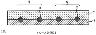
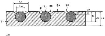
도 1a 는, 본 발명의 일 실시예의 이방성 도전 필름 (1A) 의 도전 입자의 배치를 나타내는 평면도이고, 도 1b 는 그 단면도이다. Fig. 1A is a plan view showing the arrangement of conductive particles in an anisotropic
이 이방성 도전 필름 (1A) 은, 도전 입자 (2) 가 절연성 수지 바인더 (3) 의 표면 또는 그 근방에 단층으로 배치되고, 그 위에 절연성 접착층 (4) 이 적층된 구조를 가지고 있다. This anisotropic
또한, 본 발명의 이방성 도전 필름으로는, 절연성 접착층 (4) 을 생략하고, 절연성 수지 바인더 (3) 에 도전 입자 (2) 가 매립된 구성으로 해도 된다. Further, as the anisotropic conductive film of the present invention, the insulating
<도전 입자> <Conductive particles>
도전 입자 (2) 로는, 공지된 이방성 도전 필름에 있어서 사용되고 있는 것을 적절히 선택하여 사용할 수 있다. 예를 들어, 니켈, 구리, 은, 금, 팔라듐 등의 금속 입자, 폴리아미드, 폴리벤조구아나민 등의 수지 입자의 표면을 니켈 등의 금속으로 피복한 금속 피복 수지 입자 등을 들 수 있다. 배치되는 도전 입자의 크기는, 바람직하게는 1 ∼ 30 ㎛, 보다 바람직하게는 1 ㎛ 이상 10 ㎛ 이하, 더욱 바람직하게는 2 ㎛ 이상 6 ㎛ 이하이다. As the
도전 입자 (2) 의 평균 입자경은, 화상형 내지 레이저식의 입도 분포계에 의해 측정할 수 있다. 이방성 도전 필름을 평면으로 보아 관찰하고, 입자경을 계측하여 구해도 된다. 그 경우, 바람직하게는 200 개 이상, 보다 바람직하게는 500 개 이상, 보다 더욱 바람직하게는 1000 개 이상을 계측한다. The average particle size of the
도전 입자 (2) 의 표면은, 절연 코트나 절연 입자 처리 등에 의해 피복되어 있는 것이 바람직하다. 이와 같은 피복은 도전 입자 (2) 의 표면으로부터 벗겨지기 쉽고 또한 이방성 접속에 지장을 초래하지 않는 것으로 한다. 또, 도전 입자 (2) 의 표면의 전체면 또는 일부에 돌기가 형성되어 있어도 된다. 돌기의 높이는 도전 입자경의 20 % 이내, 바람직하게는 10 % 이내인 것이 바람직하다. The surface of the
<도전 입자의 배치> <Arrangement of Conductive Particles>
(반복 유닛)(Repeating unit)
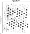
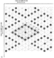
이방성 도전 필름 (1A) 의 평면으로 볼 때에 있어서의 도전 입자 (2) 의 배치는, 도전 입자열 (2p, 2q, 2r) 과 단독의 도전 입자 (2s) 가 병치된 반복 유닛 (5) 이 이방성 도전 필름 (1A) 의 전체면에 종횡 (X 방향, Y 방향) 으로 반복된 것으로 되어 있고, 반복 유닛 (5) 의 외형을 이루는 도전 입자의 중심을 순차 이어 형성되는 다각형은 3 각형으로 되어 있다. 또한, 본 발명의 이방성 도전 필름은, 필요에 따라 도전 입자가 배치되어 있지 않은 영역을 가질 수 있다. The arrangement of the
각 도전 입자열 (2p, 2q, 2r) 은, 각각 평면으로 볼 때에 도전 입자 (2) 가 간격을 두고 일렬로 직선상으로 배열되어 있다. 또, 도전 입자열 (2p, 2q, 2r) 을 구성하는 도전 입자수는 점차 상이하고, 도전 입자열 (2p, 2q, 2r) 은 평행으로 병렬되어 있다. 이와 같이 입자수가 점차 상이한 도전 입자열 (2p, 2q, 2r) 을 병렬시킨 입자 배치를 반복함으로써, 도전 입자의 개수 밀도는 국소적으로 소밀을 형성하기 때문에, 이방성 도전 필름을 전자 부품에 첩부 (貼付) 한 경우에 미소한 위치 어긋남이 있어도, 범프열을 구성하는 어느 범프에 있어서도 안정적인 수의 도전 입자를 포착시키기 쉬워진다. 이것은 이방성 도전 접속을 연속적으로 실시하는 경우에 보다 효과적이 된다. 즉, 단순한 격자 배열의 것에서 이방성 도전 필름의 전자 부품에의 첩부가 미소하게 어긋난 경우, 특히 범프 단부 (端部) 에서는 위치 어긋남의 유무나 정도에 의해 포착 입자수가 편차가 생기기 쉽다. 이 편차를 억제하기 위해서 격자 배열의 각도를 필름의 길이 방향에 대해 경사지게 하는 것이 고안되어 있다 (특허문헌 1 등). 그러나, 범프 폭이나 범프 간 거리가 보다 좁아지면, 격자 배열을 경사지게 하는 효과에는 한계가 생긴다. 이것에 대해, 본 발명에서는, 범프 길이의 범위에 도전 입자의 개수 밀도의 소밀을 발생시킴으로써, 범프 길이의 범위의 어느 지점에서는 도전 입자가 포착되도록 한다. 바꾸어 말하면, 도전 입자가 포착되는 위치와 포착되지 않는 위치를 하나의 범프에서 동시에 발생시킨다. 이로써, 범프 배열의 어디에 있어서도 범프의 형상 (면적) 이 동일하면, 반복 유닛의 반복 간격을 적절히 설정함으로써 범프에 포착되는 도전 입자의 개수가 안정되게 된다. 따라서, 이방성 도전 필름의 첩부에 미소한 위치 어긋남이 발생하였다고 해도, 또 생산 라인에서 접속체를 연속적으로 제조할 때의 접속체마다의 범프 배열에 있어서의 도전 입자의 포착 상태도 안정되기 쉬워진다. 또, 도전 입자가 포착되는 위치와 포착되지 않는 위치를 하나의 범프에서 동시에 발생시킴으로써, 이방성 도전 접속 후의 검사 노력의 저감이나 품질 관리의 향상을 기대할 수 있다. 예를 들어, 도전 입자가 포착되는 위치와 포착되지 않는 위치를 하나의 범프에서 동시에 발생시킴으로써, 이방성 도전 접속 후의 압흔 검사 시에, 연속하여 얻어진 접속체의 대비가 용이해진다. 또, 이방성 도전 접속 공정에 있어서 전자 부품에 이방성 도전 필름을 가부착했을 때의 위치 어긋남의 유무를, 연속하여 제조하는 접속체끼리에서 비교할 수 있기 때문에, 접속 장치의 개선 사항의 판정하기 쉬워지는 것을 기대할 수 있다. Each of the conductive particle rows 2p, 2q, and 2r is arranged in a line in a row with the
반복 유닛 (5) 에 있어서의 도전 입자 (2) 의 배치는, 그 반복 유닛 (5) 을 구성하는 도전 입자 (2) 의 일부가, 정 6 각형을 간극 없이 배열한 경우의 각 정 6 각형의 정점의 일부를 차지하는 배치로 되어 있다. 혹은, 정 3 각형을 간극 없이 배열한 경우의 정 3 각형의 정점과 반복 유닛 (5) 을 구성하는 도전 입자가 겹치는 배치로 되어 있다. 또한 바꾸어 말하면, 6 방 격자 배열의 각 격자점에 도전 입자가 존재하는 배치로부터 소정의 격자점의 도전 입자를 규칙적으로 제거한 나머지 배치가 반복 유닛 (5) 으로 되어 있다. 이와 같이 6 방 격자 배열의 격자점에 도전 입자 (2) 를 배치하면 반복 유닛 (5) 의 입자 배치가 인식하기 쉽고, 설계가 용이해진다. 또한, 후술하는 바와 같이, 반복 유닛에 있어서의 도전 입자의 배치는, 6 방 격자를 기본으로 하는 것으로 한정하지 않고, 정방 격자를 기본으로 해도 되고, 8 각형 이상의 정다각형을 종횡으로 배열하여, 인접하는 정다각형의 변끼리를 중첩한 배치를 기본으로 해도 된다. The arrangement of the
(반복 유닛의 반복 양태)(Repetition of repeated units)
도 1a 에 나타낸 이방성 도전 필름 (1A) 에 있어서의 반복 유닛 (5) 의 반복은, 보다 상세하게는 X 방향으로는, 반복 유닛 (5) 이, 반복 유닛 (5) 내에 있어서의 입자 간격을 두고 반복되고 있다. 또, Y 방향으로는, 반복 유닛 (5) 을 Y 방향의 대칭축으로 반전시킨 반복 유닛 (5B) 과 반복 유닛 (5) 이 간격을 두고 교대로 반복되고 있다. 이 경우, 반복 유닛의 외형을 이루는 도전 입자의 중심을 순차 이어 형성되는 다각형을, 이방성 도전 필름의 폭 방향으로 투영했을 때의 이방성 도전 필름의 길이 방향의 변에 있어서의 위치가, 그 반복 유닛에 인접하는 반복 유닛의 동일한 위치가 부분적으로 중첩되는 것이 바람직하다. 일반적으로, 전자 부품의 단자의 폭 방향이 이방성 도전 필름의 길이 방향이 되므로, 상기 서술한 바와 같이 반복 유닛의 외형을 이루는 다각형을 중첩시키면, 전자 부품의 단자에서 도전 입자가 포착될 확률이 높아지기 때문이다. 또, 이방성 도전 필름의 길이 방향과 폭 방향을 바꾸어도 된다. 단자 레이아웃에 따라서는, 바꾸는 편이 좋은 경우도 발생하기 때문이다. The repetition of the
또한, 도전 입자 (2) 의 반복 유닛을 생각하는 경우에, 반복 유닛 (5) 과 그것을 반전시킨 반복 유닛 (5B) 을 합친 유닛을 도전 입자의 반복 단위로 볼 수도 있지만, 본 발명에 있어서 반복 유닛은, 복수의 도전 입자열이 병렬하여 이루어지는 유닛으로서, 종횡으로 반복되는 최소의 단위로 하는 것이 바람직하다. In the case of considering the repeating unit of the
(반복 유닛의 크기)(Size of repeating unit)
반복 유닛 (5) 의 이방성 도전 필름의 크기나 반복 유닛 간의 거리는, 그 이방성 도전 필름 (1A) 에서 접속하는 전자 부품의 범프 폭이나 범프 간 스페이스의 크기에 따라 정하는 것이 바람직하다. The size of the anisotropic conductive film of the repeating
예를 들어, 접속 대상이 비파인 피치인 경우에는, 반복 유닛 (5) 의 이방성 도전 필름 길이 방향의 크기는, 범프 폭 또는 범프 간 스페이스 중 어느 좁은 쪽의 길이보다 작은 편이 바람직하다. 이와 같은 크기로 해도 반복 유닛 (5) 이 반복 배치되어 있음으로써, 접속에 최저한 필요한 도전 입자수를 범프에 포착시킬 수 있고, 또 접속에 관여하지 않는 도전 입자수를 줄일 수 있으므로, 이방성 도전 필름의 비용 삭감을 도모할 수 있다. 또, 반복 유닛 (5) 의 외형을 이루는 다각형의 변을 이방성 도전 필름 (1A) 의 폭 방향으로 사행시킴으로써, 장척의 이방성 도전 필름의 절제 위치에 관계 없이 안정적인 접속 성능을 얻을 수 있다. For example, when the connection object is a nonphase pitch, the size of the repeating
접속 대상이 비파인 피치인 경우의 이방성 도전 필름 길이 방향에 있어서의, 인접하는 반복 유닛 (5, 5B) 의 거리는, 당해 이방성 도전 필름에서 접속하는 전자 부품의 범프 간 스페이스보다 짧게 하는 것이 바람직하다. It is preferable that the distance between the adjacent repeating
한편, 접속 대상이 파인 피치인 경우에는, 이방성 도전 필름 길이 방향의 반복 유닛 (5, 5B) 의 크기를, 범프 간 스페이스를 걸치는 크기로 하는 것이 바람직하다. On the other hand, when the object to be connected is a fine pitch, it is preferable that the size of the repeating
또한, 파인 피치와 비파인 피치의 경계는, 일례로서 범프 폭이 30 ㎛ 미만을 파인 피치로 하고, 30 ㎛ 이상을 비파인 피치로 할 수 있다. As a boundary between the fine pitch and the non-wave pitch, for example, a bump width of less than 30 占 퐉 may be a fine pitch, and a width of 30 占 퐉 or more may be a non-wave pitch.
상기 서술한 바와 같이 반복 유닛 (5) 의 크기를 접속 대상에 따라 정할 때에, 반복 유닛 (5) 을 구성하는 도전 입자수는 5 개 이상으로 하는 것이 바람직하고, 10 개 이상이 보다 바람직하며, 20 개 이상이 더욱 바람직하다. 일반적으로, 이방성 도전 접속에 의해 접속하는 대향하는 단자 사이에는, 3 개 이상, 특히 10 개 이상의 도전 입자가 포착되는 것이 바람직하기 때문에, 반복 유닛이 대향하는 단자 사이에 끼었을 때에, 그러한 수의 도전 입자가 포착되어 있는 것을 하나의 반복 유닛의 압흔으로부터 확인할 수 있도록 하기 위해서이다. As described above, when the size of the repeating
(반복 유닛의 구체적 변형 양태)(Specific modification of the repeating unit)
본 발명에 있어서, 반복 유닛 (5) 에 있어서의 도전 입자 (2) 의 배치나, 반복 유닛 (5) 의 종횡의 반복 피치는, 이방성 도전 접속의 접속 대상으로 하는 단자의 형상이나 단자의 피치에 따라 적절히 변경할 수 있다. 따라서, 도전 입자 (2) 를 단순한 격자상의 배열로 하는 경우에 비해, 이방성 도전 필름 전체적으로는 적은 도전 입자수로 높은 포착성을 달성할 수 있다. In the present invention, the arrangement of the
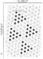
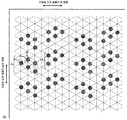
예를 들어, 도 1a 에 나타낸 반복 양태 외에, 도 2 에 나타내는 이방성 도전 필름 (1B) 과 같이, 반복 유닛 (5) 을 지그재그 배열상으로 반복해도 된다. 지그재그 배열에서는, 전자 부품의 이방성 도전 접속 시의 수지 유동이 도전 입자에 미치는 영향이, 지그재그 배열의 중앙부에 위치하는 범프와 외측에 위치하는 범프에서는 상이하고, 지그재그 배열의 중앙부의 범프에 위치하는 범프와 외측에 위치하는 범프에서는 쇼트 리스크도 상이하므로, 반복 유닛 (5) 의 형상을 적절히 변경하여 수지 유동의 흐름을 조정할 수 있다. For example, the repeating
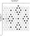
반복 유닛 (5) 에 있어서의 도전 입자 (2) 의 배치도 이방성 도전 접속의 접속 대상으로 하는 단자의 형상이나 단자의 피치에 따라 적절히 변경할 수 있다. 예를 들어, 도 3 에 나타내는 이방성 도전 필름 (1C) 과 같이, 하나의 반복 유닛 (5) 내에서 도전 입자열 (2p) 을 구성하는 도전 입자수를 점차 증가 및 감소시켜도 되고, 반복 유닛 (5) 의 반복과 함께, 단독의 도전 입자 (2s) 가 반복 배치되어도 된다. 또한, 하나의 반복 유닛 내에서 병렬하는 3 열의 도전 입자열에 있어서, 중앙의 도전 입자열을 구성하는 도전 입자수를, 양측의 도전 입자열을 구성하는 도전 입자수보다 많게 해도 적게 해도 된다. 예를 들어, 도 4 에 나타내는 이방성 도전 필름 (1D) 과 같이, 각 반복 유닛 (5) 에 있어서, 도전 입자 (2) 가 이방성 도전 필름의 길이 방향으로 4 개 배열한 도전 입자열 (2p) 과, 2 개 배열한 도전 입자열 (2q) 과, 3 개 배열한 도전 입자열 (2r) 과, 1 개의 도전 입자 (2s) 가 병렬하고 있다. 하나의 반복 유닛 내에서 병렬하는 도전 입자열에 있어서의 도전 입자의 개수를 증감시키면, 그 반복 유닛의 외형은 복잡한 다각형상이 되고, 방사상의 범프 배열 (소위, 팬 아웃 범프) 의 접속에 대응시키기 쉬워진다. 하나의 반복 유닛에 있어서의 도전 입자의 배치를, 그 반복 유닛을 구성하는 도전 입자열의 도전 입자수로 나타내고, 예를 들어 도 4 에 나타낸 반복 유닛을, [4-2-3-1] 로 나타낼 때, 이 반복 유닛의 변형예로서 [4-1-4-1], [4-3-1-2], [3-2-2-1], [4-1-2-3], [4-2-1-3] 등을 들 수 있다. 이들을 조합하여 반복 배치해도 된다. 예를 들어, [4-2-3-1-2-1-4-3] 을 들 수 있다. The arrangement of the
또, 하나의 도전 입자열 내에 있어서의 도전 입자 간 거리는, 하나의 반복 유닛 내에서 병렬하고 있는 도전 입자열끼리에서 동일해도 되고, 상이해도 된다. 예를 들어, 도 5 에 나타내는 이방성 도전 필름 (1E) 과 같이, 반복 유닛 (5) 의 외형을 마름모꼴로 하고, 그 중앙부에 도전 입자 (2) 를 배치해도 된다. 이 반복 유닛에서는, 5 개의 도전 입자로 이루어지는 도전 입자열 (2m) 과, 2 개의 도전 입자로 이루어지는 도전 입자열 (2n) 과, 3 개의 도전 입자로 이루어지는 도전 입자열 (2o) 과, 2 개의 도전 입자로 이루어지는 도전 입자열 (2p) 과, 5 개의 도전 입자로 이루어지는 도전 입자열 (2q) 이 병렬하고 있고, 도전 입자열 (2m, 2q) 에 있어서의 도전 입자 간 거리와, 도전 입자열 (2n, 2p) 에 있어서의 도전 입자 간 거리와, 도전 입자열 (2o) 에 있어서의 도전 입자 간 거리는 서로 상이하다. 이것을 전술한 표기의 [4-3-2-1] 로 한 경우, 3 의 중심의 도전 입자를 제거한 배열이어도 된다. 쇼트 발생 리스크를 보다 저감할 수 있기 때문이다. In addition, the distance between the conductive particles in one conductive particle sequence may be the same or different among the conductive particle arrays in parallel in one repeating unit. For example, as in the case of the anisotropic conductive film 1E shown in Fig. 5, the outer shape of the repeating
상기 서술한 이방성 도전 필름 (1A, 1B, 1C, 1D, 1E) 에서는, 반복 유닛 (5, 5B) 내에 있어서의 도전 입자 (2) 의 배치가 6 방 격자의 격자점에 존재하지만, 도전 입자열 (2p) 이 병렬하고 있는 한, 도 6 에 나타내는 이방성 도전 필름 (1F) 과 같이 정방 격자를 기본으로 한 배열로 해도 된다. In the above-mentioned anisotropic
도 7 에 나타내는 이방성 도전 필름 (1G) 은, 2 열의 도전 입자열 (2p, 2q) 로 이루어지는 반복 유닛 (5) 과, 그 반복 유닛 (5) 의 도전 입자의 배열축을 60°회전시킨 반복 유닛 (5B) 을 각각 필름 전체면에 반복 배치한 것이다. 이와 같이, 어느 반복 유닛과 그것을 소정 각도 회전시킨 반복 유닛을 병용해도 된다. The anisotropic conductive film 1G shown in Fig. 7 has a repeating
반복 유닛의 형상으로는, 그 외형을 이루는 도전 입자를 순차 연결하여 형성되는 다각형을 정다각형으로 해도 된다. 이것으로부터 도전 입자의 배치의 인식이 용이해지므로 바람직하다. 이 경우, 반복 유닛을 형성하는 각 도전 입자는, 6 방 격자 또는 정방 격자의 격자점에 존재하고 있지 않아도 된다. 예를 들어, 도 8 에 나타내는 이방성 도전 필름 (1H) 과 같이 반복 유닛 (5) 의 외형을 정 8 각형으로 형성할 수 있다. 이 경우, 반복 유닛의 외형을 이루는 도전 입자는, 동 도면에 파선으로 나타내는 바와 같이, 정 8 각형을 종횡으로 배열하여 인접하는 정 8 각형끼리의 변을 중첩한 격자의 그 정 8 각형의 정점에 배치되어 있다. 동일하게 하여 정 12 각형, 혹은 그 이상의 정다각형체의 정점에 도전 입자가 배치되도록 해도 된다. 또한, 6 방 격자 또는 정방 격자의 격자점에 도전 입자를 배치함으로써, 외형이 8 각형 이상의 대략 정다각형이 되는 반복 유닛을 형성해도 된다. 예를 들어, 도 9 에 나타내는 이방성 도전 필름 (1I) 의 반복 유닛 (5) 은, 정방 격자의 격자점 상에 배치된 도전 입자 (2) 로 형성되어 있고, 이방성 도전 필름의 길이 방향으로도 폭 방향으로도 대칭인 8 각형으로 되어 있다. 이로써 도전 입자의 배치를 용이하게 인식할 수 있다. As the shape of the repeating unit, a polygon formed by successively connecting conductive particles constituting the outer shape may be regular polygonal. This makes it easy to recognize the arrangement of the conductive particles, which is preferable. In this case, each of the conductive particles forming the repeating unit may not be present at the lattice point of the hexagonal lattice or the tetragonal lattice. For example, like the anisotropic conductive film 1H shown in Fig. 8, the outer shape of the repeating
또, 반복 유닛에 있어서 병렬하는 도전 입자열끼리는, 반드시 평행이 아니어도 되고, 방사상으로 배열되어 있어도 된다. 예를 들어, 도 10 에 나타내는 이방성 도전 필름 (1J) 과 같이, 방사상으로 배열한 도전 입자열 (2m, 2n, 2o, 2p, 2q) 을 갖는 반복 유닛 (5) 을 종횡으로 반복하여 배치할 수 있다. 이 경우, 도전 입자 (2) 는, 6 방 격자나 정방 격자의 격자점에 존재하지 않아도 된다. In addition, the conductive particle rows arranged in parallel in the repeating unit may not necessarily be parallel to each other, and may be radially arranged. For example, it is possible to repeatedly arrange the repeating
(반복 유닛의 변의 방향)(The direction of the side of the repeating unit)
상기 서술한 이방성 도전 필름 중, 예를 들어 도 1a 에 나타낸 이방성 도전 필름 (1A) 에서는 반복 유닛 (5) 의 외형을 이루는 도전 입자의 중심을 순차 이어 형성되는 3 각형 (5x) 의 각 변은 이방성 도전 필름 (1A) 의 길이 방향 또는 폭 방향과 사교하고 있다. 이로써, 도전 입자 (2a) 의, 이방성 도전 필름의 길이 방향의 외접선 (L1) 이, 그 도전 입자 (2a) 와 이방성 도전 필름의 길이 방향으로 인접하는 도전 입자 (2b) 를 관통한다. 또, 도전 입자 (2a) 의, 이방성 도전 필름의 폭 방향의 외접선 (L2) 이, 그 도전 입자 (2a) 와 이방성 도전 필름의 폭 방향으로 인접하는 도전 입자 (2c) 를 관통한다. 일반적으로, 이방성 도전 접속 시에는, 이방성 도전 필름의 길이 방향이 범프의 폭 방향이 되므로, 반복 유닛 (5) 의 다각형 (5x) 의 변이 이방성 도전 필름 (1A) 의 길이 방향 또는 폭 방향과 사교하고 있으면, 범프의 가장자리를 따라 복수의 도전 입자가 직선상으로 배열되는 것을 방지할 수 있고, 이로써 직선상으로 배열된 복수의 도전 입자가 한데 모여 단자로부터 벗어나 도통에 기여하지 않게 된다는 현상을 회피할 수 있으므로, 도전 입자 (2) 의 포착성을 향상시킬 수 있다.Among the above-described anisotropic conductive films, for example, in the anisotropic
또한, 이방성 도전 접속 시에 이방성 도전 필름의 길이 방향이 범프의 폭 방향이 되는 경우에, 반복 유닛 (5) 의 외형을 이루는 도전 입자로 형성되는 다각형 (5x) 은, 반드시 그 모든 변이 이방성 도전 필름의 길이 방향 또는 폭 방향과 사교하고 있지 않아도 되지만, 도전 입자의 포착성의 점에서, 바람직하게는 2 변 이상, 보다 바람직하게는 3 변 이상이 이방성 도전 필름의 길이 방향 또는 폭 방향과 사교하고 있는 것이 바람직하다. In the case where the longitudinal direction of the anisotropic conductive film is the width direction of the bump at the time of anisotropic conductive connection, the polygon 5x formed of the conductive particles constituting the outer shape of the repeating
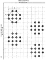
한편, 범프의 배열 패턴이 방사상인 경우 (소위, 팬 아웃 범프) 에는, 반복 유닛을 이루는 다각형이, 이방성 도전 필름의 길이 방향 또는 폭 방향의 변을 갖는 것이 바람직하다. 즉, 접속해야 할 범프끼리가, 범프가 형성되어 있는 기재의 열팽창에 의해서도 위치 어긋나지 않도록 하기 위해, 범프의 배열 패턴을 방사상으로 하는 경우가 있고 (예를 들어, 일본 공개특허공보 2007-19550호, 2015-232660호 등), 그 경우에 개개의 범프의 길이 방향과 이방성 도전 필름의 길이 방향이 이루는 각도는 점차 변화한다. 그 때문에, 반복 유닛 (5) 의 다각형의 변을 이방성 도전 필름의 길이 방향 또는 폭 방향과 사행시키지 않아도, 방사상으로 배열한 개개의 범프의 길이 방향의 가장자리에 대해 반복 유닛 (5, 5B) 의 다각형의 변은 사교한다. 따라서, 이방성 도전 접속 시에 범프의 가장자리에 걸려 있던 도전 입자의 대부분이 그 범프에 포착되지 않아, 도전 입자의 포착성이 저하한다는 현상을 회피할 수 있다. 한편, 범프의 방사상의 배열 패턴은, 통상 좌우 대칭으로 형성된다. 따라서, 이방성 도전 접속 후의 압흔에 의해 접속 상태의 양부의 확인을 용이하게 하는 점에서, 반복 유닛 (5) 의 외형을 이루는 다각형이, 이방성 도전 필름의 길이 방향 또는 폭 방향의 변을 갖는 것이 바람직하다. 그 때문에, 예를 들어 반복 유닛을 도 1a 에 나타낸 이방성 도전 필름 (1A) 과 동일한 3 각형으로 하는 경우, 도 11 에 나타낸 이방성 도전 필름 (1K) 과 같이 반복 유닛 (5) 의 외형을 이루는 3 각형의 1 변 (5a) 이 이방성 도전 필름의 길이 방향 또는 폭 방향과 평행이 되도록 배치하는 것이 바람직하다. 또, 도 8 에 나타낸 이방성 도전 필름 (1H) 의 반복 유닛 (5) 과 같이, 이방성 도전 필름의 길이 방향과 평행한 변 (5a) 과 폭 방향과 평행한 변 (5b) 을 갖게 해도 된다. On the other hand, when the arrangement pattern of the bumps is radial (so-called fan-out bump), it is preferable that the polygon forming the repeating unit has sides in the longitudinal direction or the width direction of the anisotropic conductive film. That is, in order to prevent the bumps to be connected with each other from being displaced even by the thermal expansion of the base on which the bumps are formed, the arrangement pattern of the bumps is sometimes radial (see, for example, Japanese Unexamined Patent Application Publication No. 2007-19550, 2015-232660, etc.). In that case, the angle between the longitudinal direction of the individual bumps and the longitudinal direction of the anisotropic conductive film gradually changes. Therefore, even if the sides of the polygons of the repeating
또한, 본 발명에 있어서의 도전 입자의 배치로는, 도시한 반복 유닛의 배열로 한정되지 않는다. 예를 들어, 도시한 배열을 경사지게 한 것이어도 된다. 이 경우, 90°경사지게 한 것, 즉 필름의 길이 방향과 폭 방향을 바꾼 양태도 포함된다. 또, 반복 유닛 (5) 의 간격이나 반복 유닛 내의 도전 입자의 간격을 변경한 것이어도 된다. The arrangement of the conductive particles in the present invention is not limited to the arrangement of the repeated units shown. For example, the arrangement shown may be inclined. In this case, the film is inclined by 90 DEG, that is, an aspect in which the longitudinal direction and the width direction of the film are changed. It is also possible to change the interval of the repeating
<도전 입자의 최근접 입자 간 거리><Nearest intergranular distance of conductive particles>
도전 입자의 최근접 입자 간 거리는, 반복 유닛 (5) 내에서 인접하는 도전 입자 간에 있어서도, 반복 유닛 (5) 간에서 인접하는 도전 입자 간에 있어서도, 평균 도전 입자경의 0.5 배 이상이 바람직하다. 반복 유닛 (5) 간의 거리는 반복 유닛 (5) 내에서 인접하는 도전 입자 간 거리보다 긴 것이 바람직하다. 이 거리가 지나치게 짧으면 도전 입자 상호의 접촉에 의해 쇼트가 일어나기 쉬워진다. 인접하는 도전 입자의 거리의 상한은, 범프 형상이나 범프 피치에 따라 정한다. 예를 들어, 범프 폭 200 ㎛, 범프 간 스페이스 200 ㎛ 인 경우에, 범프 폭 또는 범프 간 스페이스 중 어느 것에 도전 입자를 최저 1 개 존재시킬 때, 도전 입자 간 거리는 400 ㎛ 미만으로 한다. 도전 입자의 포착성을 확실하게 하는 점에서는, 200 ㎛ 미만으로 하는 것이 바람직하다. The nearest intergranular distance of the conductive particles is preferably 0.5 times or more of the average conductive particle diameter between the adjacent conductive particles in the repeating
<도전 입자의 개수 밀도> ≪ Number density of conductive particles &
도전 입자의 개수 밀도는, 이방성 도전 필름의 제조 비용을 억제하는 점, 및 이방성 도전 접속 시에 사용하는 압박 지그에 필요로 되는 추력이 과도하게 커지지 않도록 하는 점에서, 도전 입자의 평균 입자경이 10 ㎛ 미만인 경우, 50000 개/㎟ 이하가 바람직하고, 35000 개/㎟ 이하가 보다 바람직하며, 30000 개/㎟ 이하가 더욱 바람직하다. 한편, 도전 입자의 개수 밀도는, 지나치게 적으면 단자에서 도전 입자가 충분히 포착되지 않는 것에 의한 도통 불량이 염려되는 점에서, 300 개/㎟ 이상이 바람직하고, 500 개/㎟ 이상이 보다 바람직하며, 800 개/㎟ 이상이 더욱 바람직하다. The number density of the conductive particles is preferably in the range of 10 to 100 mu m so that the average particle diameter of the conductive particles is preferably 10 mu m or more in view of suppressing the production cost of the anisotropic conductive film and preventing the thrust required for the pressing jig used for anisotropic conductive connection from becoming excessively large. , It is preferably not more than 50000 /
또, 도전 입자의 평균 입자경이 10 ㎛ 이상인 경우에는, 15 개/㎟ 이상이 바람직하고, 50 개/㎟ 이상이 보다 바람직하며, 160 개/㎟ 이상이 보다 더욱 바람직하다. 도전 입자경이 커지면, 도전 입자의 점유 면적률도 높아지기 때문이다. 동일한 이유로부터, 1800 개/㎟ 이하가 바람직하고, 1100 개/㎟ 이하가 보다 바람직하며, 800 개/㎟ 이하가 더욱 바람직하다. When the average particle diameter of the conductive particles is 10 占 퐉 or more, the number is preferably 15 / mm2 or more, more preferably 50 / mm2 or more, and even more preferably 160 / mm2 or more. This is because, when the conductive particle diameter becomes larger, the area occupied by the conductive particles becomes higher. For the same reason, it is preferably 1800 pieces /
또한, 도전 입자의 개수 밀도는, 국소적 (일례로서 200 ㎛ × 200 ㎛) 으로는, 상기 서술한 개수 밀도를 벗어나 있어도 된다. Further, the number density of the conductive particles may be local (e.g., 200 占 퐉 占 200 占 퐉) and may deviate from the above-described number density.
<절연성 수지 바인더> ≪ Insulating resin binder &
절연성 수지 바인더 (3) 로는, 공지된 이방성 도전 필름에 있어서 절연성 수지 바인더로서 사용되고 있는 열중합성 조성물, 광중합성 조성물, 광열 병용 중합성 조성물 등을 적절히 선택하여 사용할 수 있다. 이 중 열중합성 조성물로는, 아크릴레이트 화합물과 열라디칼 중합 개시제를 포함하는 열라디칼 중합성 수지 조성물, 에폭시 화합물과 열카티온 중합 개시제를 포함하는 열카티온 중합성 수지 조성물, 에폭시 화합물과 열아니온 중합 개시제를 포함하는 열아니온 중합성 수지 조성물 등을 들 수 있고, 광중합성 조성물로는, 아크릴레이트 화합물과 광라디칼 중합 개시제를 포함하는 광라디칼 중합성 수지 조성물 등을 들 수 있다. 특히 문제가 생기지 않는 것이면, 복수종의 중합성 조성물을 병용해도 된다. 병용예로는, 열카티온 중합성 조성물과 열라디칼 중합성 조성물의 병용 등을 들 수 있다. As the insulating
여기서, 광중합 개시제로는 파장이 상이한 광에 반응하는 복수 종류를 함유시켜도 된다. 이로써, 이방성 도전 필름의 제조 시에 있어서의, 절연성 수지층을 구성하는 수지의 광경화와, 이방성 접속 시에 전자 부품끼리를 접착하기 위한 수지의 광경화에서 사용하는 파장을 구분하여 사용할 수 있다. Here, as the photopolymerization initiator, a plurality of types which react with light having a different wavelength may be contained. This makes it possible to separately use the wavelengths used in the photocuring of the resin constituting the insulating resin layer and in the photocuring of the resin for adhering the electronic components at the time of anisotropic connection in the production of the anisotropic conductive film.
절연성 수지 바인더 (3) 를 광중합성 조성물을 사용하여 형성하는 경우에, 이방성 도전 필름의 제조 시의 광경화에 의해, 절연성 수지 바인더 (3) 에 포함되는 광중합성 화합물의 전부 또는 일부를 광경화시킬 수 있다. 이 광경화에 의해, 절연성 수지 바인더 (3) 에 있어서의 도전 입자 (2) 의 배치가 유지 내지 고정화되어, 쇼트의 억제와 포착의 향상이 예상된다. 또, 이 광경화의 조건을 조정함으로써, 이방성 도전 필름의 제조 공정에 있어서의 절연성 수지층의 점도를 조정할 수 있다. When the insulating
절연성 수지 바인더 (3) 에 있어서의 광중합성 화합물의 배합량은 30 질량% 이하가 바람직하고, 10 질량% 이하가 보다 바람직하며, 2 질량% 미만이 보다 바람직하다. 광중합성 화합물이 지나치게 많으면 이방성 도전 접속 시의 압입에 가해지는 추력이 증가하기 때문이다. The compounding amount of the photopolymerizable compound in the insulating
한편, 열중합성 조성물은, 열중합성 화합물과 열중합 개시제를 함유하지만, 이 열중합성 화합물로서 광중합성 화합물로서도 기능하는 것을 사용해도 된다. 또, 열중합성 조성물에는, 열중합성 화합물과는 별도로 광중합성 화합물을 함유시킴과 함께 광중합성 개시제를 함유시켜도 된다. 바람직하게는, 열중합성 화합물과는 별도로 광중합성 화합물과 광중합 개시제를 함유시킨다. 예를 들어, 열중합 개시제로서 열카티온계 중합 개시제, 열중합성 화합물로서 에폭시 수지를 사용하고, 광중합 개시제로서 광라디칼 개시제, 광중합성 화합물로서 아크릴레이트 화합물을 사용한다. 절연성 수지 바인더 (3) 에는, 이들 중합성 조성물의 경화물을 포함해도 된다. On the other hand, the thermosetting composition contains a thermosetting compound and a thermal polymerization initiator, but the thermosetting compound that functions as a photopolymerizable compound may also be used. The thermosetting composition may contain a photopolymerizable compound separately from the thermopolymerizable compound, and may contain a photopolymerization initiator. Preferably, a photopolymerizable compound and a photopolymerization initiator are contained separately from the thermopolymerizable compound. For example, a thermal curing type polymerization initiator is used as a thermal polymerization initiator, an epoxy resin is used as a heat curing compound, a photo radical initiator is used as a photopolymerization initiator, and an acrylate compound is used as a photopolymerizable compound. The insulating
열 또는 광중합성 화합물로서 사용되는 아크릴레이트 화합물로는 종래 공지된 열중합형 (메트)아크릴레이트 모노머를 사용할 수 있다. 예를 들어, 단관능 (메트)아크릴레이트계 모노머, 2 관능 이상의 다관능 (메트)아크릴레이트계 모노머를 사용할 수 있다. As the acrylate compound used as a heat or photopolymerizable compound, conventionally known heat polymerization type (meth) acrylate monomers can be used. For example, monofunctional (meth) acrylate monomers and bifunctional or higher polyfunctional (meth) acrylate monomers can be used.
또, 중합성 화합물로서 사용되는 에폭시 화합물은, 3 차원 망목 구조를 형성하고, 양호한 내열성, 접착성을 부여하는 것이고, 고형 에폭시 수지와 액상 에폭시 수지를 병용하는 것이 바람직하다. 여기서, 고형 에폭시 수지란, 상온에서 고체인 에폭시 수지를 의미한다. 또, 액상 에폭시 수지란, 상온에서 액상인 에폭시 수지를 의미한다. 또, 상온이란, JIS Z 8703 에서 규정된 5 ∼ 35 ℃ 의 온도 범위를 의미한다. 본 발명에서는 2 종 이상의 에폭시 화합물을 병용할 수 있다. 또, 에폭시 화합물에 추가하여 옥세탄 화합물을 병용해도 된다. The epoxy compound used as the polymerizable compound forms a three-dimensional network structure, imparts good heat resistance and adhesion, and is preferably used in combination with a solid epoxy resin and a liquid epoxy resin. Here, the solid epoxy resin means an epoxy resin which is solid at room temperature. The liquid epoxy resin means an epoxy resin which is liquid at room temperature. The room temperature means a temperature range of 5 to 35 ° C specified in JIS Z 8703. In the present invention, two or more kinds of epoxy compounds can be used in combination. In addition to the epoxy compound, an oxetane compound may be used in combination.
고형 에폭시 수지로는, 액상 에폭시 수지와 상용하고, 상온에서 고체이면 특별히 한정되지 않고, 비스페놀 A 형 에폭시 수지, 비스페놀 F 형 에폭시 수지, 다관능형 에폭시 수지, 디시클로펜타디엔형 에폭시 수지, 노볼락페놀형 에폭시 수지, 비페닐형 에폭시 수지, 나프탈렌형 에폭시 수지 등을 들 수 있고, 이들 중에서 1 종을 단독으로, 또는 2 종 이상을 조합하여 사용할 수 있다. 이들 중에서도, 비스페놀 A 형 에폭시 수지를 사용하는 것이 바람직하다. The solid epoxy resin is not particularly limited as long as it is compatible with a liquid epoxy resin and is solid at room temperature, and examples thereof include bisphenol A type epoxy resin, bisphenol F type epoxy resin, multifunctional epoxy resin, dicyclopentadiene type epoxy resin, Type epoxy resin, a biphenyl-type epoxy resin, and a naphthalene-type epoxy resin. Of these, one type may be used alone, or two or more types may be used in combination. Of these, it is preferable to use a bisphenol A type epoxy resin.
액상 에폭시 수지로는, 상온에서 액상이면 특별히 한정되지 않고, 비스페놀 A 형 에폭시 수지, 비스페놀 F 형 에폭시 수지, 노볼락페놀형 에폭시 수지, 나프탈렌형 에폭시 수지 등을 들 수 있고, 이들 중에서 1 종을 단독으로, 또는 2 종 이상을 조합하여 사용할 수 있다. 특히, 필름의 택성, 유연성 등의 관점에서, 비스페놀 A 형 에폭시 수지를 사용하는 것이 바람직하다. The liquid epoxy resin is not particularly limited as long as it is liquid at room temperature, and examples thereof include bisphenol A type epoxy resin, bisphenol F type epoxy resin, novolak phenol type epoxy resin and naphthalene type epoxy resin. Or a combination of two or more. Particularly, from the viewpoint of tackiness and flexibility of the film, it is preferable to use a bisphenol A type epoxy resin.
열중합 개시제 중 열라디칼 중합 개시제로는, 예를 들어 유기 과산화물, 아조계 화합물 등을 들 수 있다. 특히, 기포의 원인이 되는 질소를 발생하지 않는 유기 과산화물을 바람직하게 사용할 수 있다. Examples of thermal radical polymerization initiators among the thermal polymerization initiators include organic peroxides and azo-based compounds. Particularly, organic peroxides which do not generate nitrogen which causes bubbles can be preferably used.
열라디칼 중합 개시제의 사용량은, 지나치게 적으면 경화 불량이 되고, 지나치게 많으면 제품 라이프의 저하가 되므로, (메트)아크릴레이트 화합물 100 질량부에 대해, 바람직하게는 2 ∼ 60 질량부, 보다 바람직하게는 5 ∼ 40 질량부이다. If the amount of the thermal radical polymerization initiator used is too small, the curing becomes defective. When the amount is too large, the life of the product deteriorates. Therefore, the amount is preferably 2 to 60 parts by mass, more preferably 2 to 60 parts by mass with respect to 100 parts by mass of the (meth) 5 to 40 parts by mass.
열카티온 중합 개시제로는, 에폭시 화합물의 열카티온 중합 개시제로서 공지된 것을 채용할 수 있고, 예를 들어 열에 의해 산을 발생하는 요오드늄염, 술포늄염, 포스포늄염, 페로센류 등을 사용할 수 있고, 특히 온도에 대해 양호한 잠재성을 나타내는 방향족 술포늄염을 바람직하게 사용할 수 있다. As the thermal cationic polymerization initiator, those known as a thermal cationic polymerization initiator of an epoxy compound can be employed. For example, iodonium salts, sulfonium salts, phosphonium salts, and ferrocenes which generate an acid by heat can be used And particularly preferably an aromatic sulfonium salt exhibiting a good potential with respect to temperature.
열카티온 중합 개시제의 사용량은, 지나치게 적어도 경화 불량이 되는 경향이 있고, 지나치게 많아도 제품 라이프가 저하하는 경향이 있으므로, 에폭시 화합물 100 질량부에 대해 바람직하게는 2 ∼ 60 질량부, 보다 바람직하게는 5 ∼ 40 질량부이다. The amount of the thermal cation polymerization initiator to be used tends to be excessively poor at least at a curing rate, and if too large, the product life tends to deteriorate. Therefore, the amount is preferably 2 to 60 parts by mass, 5 to 40 parts by mass.
열아니온 중합 개시제로는, 통상 사용되는 공지된 것을 사용할 수 있다. 예를 들어, 유기산 디하이드라지드, 디시안디아미드, 아민 화합물, 폴리아미드아민 화합물, 시아네이트에스테르 화합물, 페놀 수지, 산 무수물, 카르복실산, 3 급 아민 화합물, 이미다졸, 루이스산, 브렌스테드산염, 폴리메르캅탄계 경화제, 우레아 수지, 멜라민 수지, 이소시아네이트 화합물, 블록 이소시아네이트 화합물 등을 들 수 있고, 이들 중에서 1 종을 단독으로, 또는 2 종 이상을 조합하여 사용할 수 있다. 이들 중에서도, 이미다졸 변성체를 핵으로 하고 그 표면을 폴리우레탄으로 피복하여 이루어지는 마이크로캡슐형 잠재성 경화제를 사용하는 것이 바람직하다. As the thermal polymerization initiator, conventionally known ones can be used. For example, there may be mentioned organic acid dihydrazide, dicyandiamide, amine compound, polyamide amine compound, cyanate ester compound, phenol resin, acid anhydride, carboxylic acid, tertiary amine compound, imidazole, Lewis acid, Urethane resins, melamine resins, isocyanate compounds, and block isocyanate compounds. Of these, one type may be used alone, or two or more types may be used in combination. Among them, it is preferable to use a microcapsule type latent curing agent comprising an imidazole modified product as a nucleus and its surface coated with polyurethane.
열중합성 조성물에는, 막 형성 수지를 함유시키는 것이 바람직하다. 막 형성 수지는, 예를 들어 평균 분자량이 10000 이상인 고분자량 수지에 상당하고, 필름 형성성의 관점에서, 10000 ∼ 80000 정도의 평균 분자량인 것이 바람직하다. 막 형성 수지로는, 페녹시 수지, 폴리에스테르 수지, 폴리우레탄 수지, 폴리에스테르우레탄 수지, 아크릴 수지, 폴리이미드 수지, 부티랄 수지 등 여러 가지 수지를 들 수 있고, 이들은 단독으로 사용해도 되고, 2 종류 이상을 조합하여 사용해도 된다. 이들 중에서도, 막 형성 상태, 접속 신뢰성 등의 관점에서 페녹시 수지를 적절히 사용하는 것이 바람직하다. The thermosetting composition preferably contains a film-forming resin. The film-forming resin corresponds to, for example, a high molecular weight resin having an average molecular weight of 10,000 or more, and is preferably an average molecular weight of about 10,000 to 80,000 from the viewpoint of film formability. As the film-forming resin, various resins such as a phenoxy resin, a polyester resin, a polyurethane resin, a polyester urethane resin, an acrylic resin, a polyimide resin, and a butyral resin may be used. Or more may be used in combination. Among these, it is preferable to use a phenoxy resin suitably from the viewpoints of film formation state, connection reliability, and the like.
열중합성 조성물에는, 용융 점도 조정을 위해서, 절연성 필러를 함유시켜도 된다. 이것은 실리카분이나 알루미나분 등을 들 수 있다. 절연성 필러의 크기는 입경 20 ∼ 1000 nm 가 바람직하고, 또 배합량은 에폭시 화합물 등의 열중합성 화합물 (광중합성 화합물) 100 질량부에 대해 5 ∼ 50 질량부로 하는 것이 바람직하다. The thermosetting composition may contain an insulating filler for adjusting the melt viscosity. These include silica powder and alumina powder. The insulating filler preferably has a particle size of 20 to 1000 nm, and the amount of the insulating filler is preferably 5 to 50 parts by mass based on 100 parts by mass of a heat-polymerizable compound such as an epoxy compound (photopolymerizable compound).
또한, 상기 서술한 절연성 필러와는 상이한 충전제, 연화제, 촉진제, 노화 방지제, 착색제 (안료, 염료), 유기 용제, 이온 캐처제 등을 함유시켜도 된다. Further, a filler, a softener, an accelerator, an antioxidant, a coloring agent (pigment, dye), an organic solvent, an ion catcher and the like which are different from the above-described insulating filler may be contained.
또, 필요에 따라 응력 완화제, 실란 커플링제, 무기 필러 등을 배합해도 된다. 응력 완화제로는, 수소 첨가 스티렌-부타디엔 블록 공중합체, 수소 첨가 스티렌-이소프렌 블록 공중합체 등을 들 수 있다. 또, 실란 커플링제로는, 에폭시계, 메타크릴옥시계, 아미노계, 비닐계, 메르캅토·술파이드계, 우레이드계 등을 들 수 있다. 또, 무기 필러로는, 실리카, 탤크, 산화티탄, 탄산칼슘, 산화마그네슘 등을 들 수 있다. If necessary, a stress relaxation agent, a silane coupling agent, an inorganic filler, or the like may be added. Examples of the stress relaxation agent include hydrogenated styrene-butadiene block copolymer and hydrogenated styrene-isoprene block copolymer. Examples of the silane coupling agent include an epoxy type, a methacryloyloxy type, an amino type, a vinyl type, a mercapto and sulfide type, and an ureide type. Examples of the inorganic filler include silica, talc, titanium oxide, calcium carbonate, magnesium oxide, and the like.
절연성 수지 바인더 (3) 는, 상기 서술한 수지를 포함하는 코팅 조성물을 도포법에 의해 성막하고 건조시키는 것이나, 추가로 경화시키는 것에 의해, 혹은 미리 공지된 수법에 의해 필름화하는 것에 의해 형성할 수 있다. 절연성 수지 바인더 (3) 는, 필요에 따라 수지층을 적층하는 것에 의해 얻어도 된다. 또, 절연성 수지 바인더 (3) 는, 박리 처리된 폴리에틸렌테레프탈레이트 필름 등의 박리 필름 상에 형성하는 것이 바람직하다. The insulating
(절연성 수지 바인더의 점도) (Viscosity of insulating resin binder)
절연성 수지 바인더 (3) 의 최저 용융 점도는 이방성 도전 필름의 제조 방법 등에 따라 적절히 정할 수 있다. 예를 들어, 이방성 도전 필름의 제조 방법으로서, 도전 입자를 절연성 수지 바인더의 표면에 소정의 배치로 유지시키고, 그 도전 입자를 절연성 수지 바인더에 압입하는 방법을 실시할 때, 절연성 수지 바인더가 필름 성형을 가능하게 하는 점에서 수지의 최저 용융 점도를 1100 Pa·s 이상으로 하는 것이 바람직하다. 또, 후술하는 바와 같이, 도 12 또는 도 13 에 나타내는 바와 같이 절연성 수지 바인더 (3) 에 압입한 도전 입자 (2) 의 노출 부분의 둘레에 함몰 (3b) 을 형성하거나, 도 14 에 나타내는 바와 같이 절연성 수지 바인더 (3) 에 압입한 도전 입자 (2) 의 바로 위에 함몰 (3c) 을 형성하거나 하는 점에서, 최저 용융 점도는, 바람직하게는 1500 Pa·s 이상, 보다 바람직하게는 2000 Pa·s 이상, 더욱 바람직하게는 3000 ∼ 15000 Pa·s, 특히 3000 ∼ 10000 Pa·s 이다. 이 최저 용융 점도는, 일례로서 회전식 레오미터 (TA instrument 사 제조) 를 이용하고, 승온 속도가 10 ℃/분, 측정 압력이 5 g 로 일정하게 유지하고, 직경 8 mm 의 측정 플레이트를 사용하여 구할 수 있다. 또, 바람직하게는 40 ∼ 80 ℃, 보다 바람직하게는 50 ∼ 60 ℃ 에서 절연성 수지 바인더 (3) 에 도전 입자 (2) 를 압입하는 공정을 실시하는 경우에, 상기 서술과 마찬가지로 함몰 (3b 또는 3c) 의 형성의 점에서, 60 ℃ 에 있어서의 점도는, 하한은 바람직하게는 3000 Pa·s 이상, 보다 바람직하게는 4000 Pa·s 이상, 더욱 바람직하게는 4500 Pa·s 이상이고, 상한은, 바람직하게는 20000 Pa·s 이하, 보다 바람직하게는 15000 Pa·s 이하, 더욱 바람직하게는 10000 Pa·s 이하이다. The minimum melt viscosity of the insulating resin binder (3) can be suitably determined according to the production method of the anisotropic conductive film and the like. For example, when a method for manufacturing an anisotropic conductive film is employed in which a conductive particle is held on a surface of an insulating resin binder in a predetermined arrangement and the conductive particle is pressed into an insulating resin binder, The minimum melt viscosity of the resin is preferably 1100 Pa · s or more. 12 or 13, a
절연성 수지 바인더 (3) 를 구성하는 수지의 점도를 상기 서술한 바와 같이 고점도로 함으로써, 이방성 도전 필름의 사용 시에 있어서, 대향하는 전자 부품 등의 접속 대상물 사이에 도전 입자 (2) 를 끼우고 가열 가압하는 경우에, 이방성 도전 필름 내의 도전 입자 (2) 가, 용융한 절연성 수지 바인더 (3) 의 유동에 의해 흐르게 되어 버리는 것을 방지할 수 있다. By setting the viscosity of the resin constituting the insulating
(절연성 수지 바인더의 두께) (Thickness of insulating resin binder)
절연성 수지 바인더 (3) 의 두께 (La) 는, 바람직하게는 1 ㎛ 이상 60 ㎛ 이하, 보다 바람직하게는 1 ㎛ 이상 30 ㎛ 이하, 더욱 바람직하게는 2 ㎛ 이상 15 ㎛ 이하이다. 또, 절연성 수지 바인더 (3) 의 두께 (La) 는, 도전 입자 (2) 의 평균 입자경 (D) 과의 관계에서는, 그들의 비 (La/D) 가 0.6 ∼ 10 이 바람직하다. 절연성 수지 바인더 (3) 의 두께 (La) 가 지나치게 크면 이방성 도전 접속 시에 도전 입자가 위치 어긋나기 쉬워지고, 단자에 있어서의 도전 입자의 포착성이 저하한다. 이 경향은 La/D 가 10 을 초과하면 현저하다. 그래서 La/D 는 8 이하가 보다 바람직하고, 6 이하가 보다 더욱 바람직하다. 반대로 절연성 수지 바인더 (3) 의 두께 (La) 가 지나치게 작아 La/D 가 0.6 미만이 되면, 도전 입자를 절연성 수지 바인더 (3) 에 의해 소정의 입자 분산 상태 혹은 소정의 배열로 유지하는 것이 곤란해진다. 특히, 접속하는 단자가 고밀도 COG 인 경우, 절연성 수지 바인더 (3) 의 층두께 (La) 와 도전 입자 (2) 의 입자경 (D) 의 비 (La/D) 는, 바람직하게는 0.8 ∼ 2 이다. The thickness La of the insulating
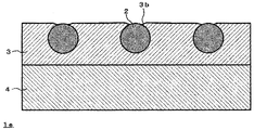
(절연성 수지 바인더에 있어서의 도전 입자의 매립 양태) (Bonding of Conductive Particles in Insulating Resin Binder)
절연성 수지 바인더 (3) 에 있어서의 도전 입자 (2) 의 매립 상태에 대해서는 특별히 제한이 없지만, 이방성 도전 필름을 대향하는 부품 사이에서 협지하고, 가열 가압함으로써 이방성 도전 접속을 실시하는 경우, 도 12, 도 13 에 나타내는 바와 같이, 도전 입자 (2) 를 절연성 수지 바인더 (3) 로부터 부분적으로 노출시켜, 인접하는 도전 입자 (2) 간의 중앙부에 있어서의 절연성 수지 바인더의 표면 (3a) 의 접평면 (3P) 에 대해 도전 입자 (2) 의 노출 부분의 둘레에 함몰 (3b) 이 형성되어 있거나, 또는 도 14 에 나타내는 바와 같이, 절연성 수지 바인더 (3) 내에 압입된 도전 입자 (2) 의 바로 위의 절연성 수지 바인더 부분에, 상기와 동일한 접평면 (3P) 에 대해 함몰 (3c) 이 형성되고, 도전 입자 (2) 의 바로 위의 절연성 수지 바인더 (3) 의 표면에 굴곡이 존재하도록 하는 것이 바람직하다. 도전 입자 (2) 가 대향하는 전자 부품의 전극 사이에서 협지되어 가열 가압될 때에 생기는 도전 입자 (2) 의 편평화에 대해, 도 12, 도 13 에 나타낸 함몰 (3b) 이 있는 것으로부터, 도전 입자 (2) 가 절연성 수지 바인더 (3) 로부터 받는 저항이, 함몰 (3b) 이 없는 경우에 비해 저감한다. 이 때문에, 대향하는 전극 간에 있어서 도전 입자 (2) 가 협지되기 쉬워져, 도통 성능도 향상된다. 또, 절연성 수지 바인더 (3) 를 구성하는 수지 중, 도전 입자 (2) 의 바로 위의 수지의 표면에 함몰 (3c)(도 14) 이 형성되어 있음으로써, 함몰 (3c) 이 없는 경우에 비해 가열 가압 시의 압력이 도전 입자 (2) 에 집중하기 쉬워져, 전극에 있어서 도전 입자 (2) 가 협지되기 쉬워져, 도통 성능이 향상된다. Although the embedding state of the
상기 서술한 함몰 (3b, 3c) 의 효과를 얻기 쉽게 하는 점에서, 도전 입자 (2) 의 노출 부분의 둘레의 함몰 (3b)(도 12, 도 13) 의 최대 깊이 (Le) 와 도전 입자 (2) 의 평균 입자경 (D) 의 비 (Le/D) 는, 바람직하게는 50 % 미만, 보다 바람직하게는 30 % 미만, 더욱 바람직하게는 20 ∼ 25 % 이고, 도전 입자 (2) 의 노출 부분의 둘레의 함몰 (3b)(도 12, 도 13) 의 최대 직경 (Ld) 과 도전 입자 (2) 의 평균 입자경 (D) 의 비 (Ld/D) 는, 바람직하게는 100 % 이상, 보다 바람직하게는 100 ∼ 150 % 이고, 도전 입자 (2) 의 바로 위의 수지에 있어서의 함몰 (3c)(도 14) 의 최대 깊이 (Lf) 와 도전 입자 (2) 의 평균 입자경 (D) 의 비 (Lf/D) 는, 바람직하게는 0 보다 크고, 바람직하게는 10 % 미만, 보다 바람직하게는 5 % 미만이다. The maximum depth Le of the
또한, 도전 입자 (2) 의 노출 부분의 직경 (Lc) 은, 도전 입자 (2) 의 평균 입자경 (D) 이하로 할 수 있고, 바람직하게는 평균 입자경 (D) 의 10 ∼ 90 % 이다. 도전 입자 (2) 의 정부 (頂部)(2t) 의 1 점에서 노출되도록 해도 되고, 도전 입자 (2) 가 절연성 수지 바인더 (3) 내에 완전히 묻혀, 직경 (Lc) 이 제로가 되도록 해도 된다. The diameter Lc of the exposed portion of the
(절연성 수지 바인더의 두께 방향에 있어서의 도전 입자의 위치) (Position of the conductive particles in the thickness direction of the insulating resin binder)
상기 서술한 함몰 (3b) 의 효과를 얻기 쉽게 하는 점에서, 인접하는 도전 입자 (2) 간의 중앙부에 있어서의 절연성 수지 바인더의 표면 (3a) 의 접평면 (3p) 으로부터의 도전 입자 (2) 의 최심부의 거리 (이하, 매립량이라고 한다)(Lb) 와, 도전 입자 (2) 의 평균 입자경 (D) 의 비 (Lb/D)(이하, 매립률이라고 한다) 는 60 % 이상 105 % 이하인 것이 바람직하다. (3b) of the conductive particles (2) from the tangent plane (3p) of the surface (3a) of the insulating resin binder at the central portion between the adjacent conductive particles (2) The ratio Lb / D of the average particle diameter D of the conductive particles 2 (hereinafter referred to as the filling amount) Lb (hereinafter referred to as the filling amount) (hereinafter referred to as the filling ratio) is not less than 60% nor more than 105% desirable.
<절연성 접착층> <Insulating Adhesive Layer>
본 발명의 이방성 도전 필름에서는, 도전 입자 (2) 를 배치시키고 있는 절연성 수지 바인더 (3) 상에, 절연성 수지 바인더 (3) 를 구성하는 수지와 점도나 점착성이 상이한 절연성 접착층 (4) 이 적층되어 있어도 된다. In the anisotropic conductive film of the present invention, the insulating
절연성 수지 바인더 (3) 에 상기 서술한 함몰 (3b) 이 형성되어 있는 경우, 도 15 에 나타내는 이방성 도전 필름 (1d) 과 같이, 절연성 접착층 (4) 은, 절연성 수지 바인더 (3) 에 함몰 (3b) 이 형성되어 있는 면에 적층되어도 되고, 도 16 에 나타내는 이방성 도전 필름 (1e) 과 같이, 함몰 (3b) 이 형성되어 있는 면과 반대측의 면에 적층되어도 된다. 절연성 수지 바인더 (3) 에 함몰 (3c) 이 형성되어 있는 경우도 동일하다. 절연성 접착층 (4) 의 적층에 의해, 이방성 도전 필름을 사용하여 전자 부품을 이방성 도전 접속할 때에, 전자 부품의 전극이나 범프에 의해 형성되는 공간을 충전하여, 접착성을 향상시킬 수 있다. 15, the insulating
또, 절연성 접착층 (4) 을 절연성 수지 바인더 (3) 에 적층하는 경우, 절연성 접착층 (4) 이 함몰 (3b, 3c) 의 형성면 상에 있는지 여부에 관계 없이, 절연성 접착층 (4) 이 IC 칩 등의 제 1 전자 부품측에 있는 (바꾸어 말하면, 절연성 수지 바인더 (3) 가 기판 등의 제 2 전자 부품측에 있다) 것이 바람직하다. 이와 같이 함으로써, 도전 입자의 의도하지 않은 이동을 피할 수 있어, 포착성을 향상시킬 수 있다. 또한, 통상은 IC 칩 등의 제 1 전자 부품을 압박 지그측으로 하고, 기판 등의 제 2 전자 부품을 스테이지측으로 하고, 이방성 도전 필름을 제 2 전자 부품과 가압착한 후에, 제 1 전자 부품과 제 2 전자 부품을 본압착하지만, 제 2 전자 부품의 열압착 영역의 사이즈 등에 따라서는, 이방성 도전 필름을 제 1 전자 부품과 가부착한 후에, 제 1 전자 부품과 제 2 전자 부품을 본압착한다. When the insulating
절연성 접착층 (4) 으로는, 공지된 이방성 도전 필름에 있어서 절연성 접착층으로서 사용되고 있는 것을 적절히 선택하여 사용할 수 있다. 절연성 접착층 (4) 은, 상기 서술한 절연성 수지 바인더 (3) 와 동일한 수지를 사용하여 점도를 보다 낮게 조정한 것으로 해도 된다. 절연성 접착층 (4) 과 절연성 수지 바인더 (3) 의 최저 용융 점도는, 차가 있을수록 전자 부품의 전극이나 범프에 의해 형성되는 공간이 절연성 접착층 (4) 으로 충전되기 쉬워져, 전자 부품끼리의 접착성을 향상시키는 효과를 기대할 수 있다. 또, 이 차가 있을수록 이방성 도전 접속 시에 절연성 수지 바인더 (3) 를 구성하는 수지의 이동량이 상대적으로 작아지기 때문에, 단자에 있어서의 도전 입자의 포착성이 향상되기 쉬워진다. 실용상은, 절연성 접착층 (4) 과 절연성 수지 바인더 (3) 의 최저 용융 점도비는, 바람직하게는 2 이상, 보다 바람직하게는 5 이상, 더욱 바람직하게는 8 이상이다. 한편, 이 비가 지나치게 크면 장척의 이방성 도전 필름을 권장체 (卷裝體) 로 한 경우에, 수지의 돌출이나 블로킹이 생길 우려가 있으므로, 실용상은 15 이하가 바람직하다. 절연성 접착층 (4) 의 바람직한 최저 용융 점도는, 보다 구체적으로는 상기 서술한 비를 만족하고, 또한 3000 Pa·s 이하, 보다 바람직하게는 2000 Pa·s 이하이고, 특히 100 ∼ 2000 Pa·s 이다. As the insulating
절연성 접착층 (4) 의 형성 방법으로는, 절연성 수지 바인더 (3) 를 형성하는 수지와 동일한 수지를 포함하는 코팅 조성물을 도포법에 의해 성막하고 건조시키는 것이나, 추가로 경화시키는 것에 의해, 혹은 미리 공지된 수법에 의해 필름화하는 것에 의해 형성할 수 있다. The insulating
절연성 접착층 (4) 의 두께는, 바람직하게는 1 ㎛ 이상 30 ㎛ 이하, 보다 바람직하게는 2 ㎛ 이상 15 ㎛ 이하이다. The thickness of the insulating
또, 절연성 수지 바인더 (3) 와 절연성 접착층 (4) 을 합한 이방성 도전 필름 전체의 최저 용융 점도는, 절연성 수지 바인더 (3) 와 절연성 접착층 (4) 의 두께의 비율에 따라 다르기도 하지만, 실용상은 8000 Pa·s 이하로 해도 되고, 범프 사이에의 충전을 실시하기 쉽게 하기 위해서는 200 ∼ 7000 Pa·s 여도 되고, 바람직하게는 200 ∼ 4000 Pa·s 이다. The minimum melt viscosity of the entire anisotropic conductive film including the insulating
절연성 수지 바인더 (3) 나 절연성 접착층 (4) 에는, 필요에 따라 실리카 미립자, 알루미나, 수산화알루미늄 등의 절연성 필러를 첨가해도 된다. 절연성 필러의 배합량은, 그들의 층을 구성하는 수지 100 질량부에 대해 3 질량부 이상 40 질량부 이하로 하는 것이 바람직하다. 이로써, 이방성 도전 접속 시에 이방성 도전 필름이 용융해도, 용융한 수지에 의해 도전 입자가 불필요하게 이동하는 것을 억제할 수 있다. To the insulating
<이방성 도전 필름의 제조 방법> ≪ Anisotropic conductive film production method >
이방성 도전 필름의 제조 방법으로는, 예를 들어 도전 입자를 소정의 배열로 배치하기 위한 전사형을 제조하고, 전사형의 오목부에 도전 입자를 충전하고, 그 위에 박리 필름 상에 형성한 절연성 수지 바인더 (3) 를 덮고 압력을 가하여, 절연성 수지 바인더 (3) 에 도전 입자 (2) 를 압입함으로써, 절연성 수지 바인더 (3) 에 도전 입자 (2) 를 전착시킨다. 혹은 추가로 그 도전 입자 (2) 상에 절연성 접착층 (4) 을 적층한다. 이렇게 하여, 이방성 도전 필름 (1A) 을 얻을 수 있다. The anisotropic conductive film may be produced, for example, by preparing a transfer type for arranging conductive particles in a predetermined arrangement, filling the transfer type recess with conductive particles, and forming an insulating resin binder (for example, The
또, 전사형의 오목부에 도전 입자를 충전한 후, 그 위에 절연성 수지 바인더를 덮고, 전사형으로부터 절연성 수지 바인더의 표면에 도전 입자를 전사시키고, 절연성 수지 바인더 상의 도전 입자를 절연성 수지 바인더 내로 압입함으로써 이방성 도전 필름을 제조해도 된다. 이 압입 시의 압박력, 온도 등에 의해 도전 입자의 매립량 (Lb) 을 조정할 수 있다. 또, 함몰 (3b, 3c) 의 형상 및 깊이를, 압입 시의 절연성 수지 바인더의 점도, 압입 속도, 온도 등에 의해 조정할 수 있다. 예를 들어, 도전 입자의 압입 시의 절연성 수지 바인더의 점도를, 하한은 바람직하게는 3000 Pa·s 이상, 보다 바람직하게는 4000 Pa·s 이상, 더욱 바람직하게는 4500 Pa·s 이상으로 하고, 상한은, 바람직하게는 20000 Pa·s 이하, 보다 바람직하게는 15000 Pa·s 이하, 더욱 바람직하게는 10000 Pa·s 이하로 한다. 또, 이와 같은 점도를 바람직하게는 40 ∼ 80 ℃, 보다 바람직하게는 50 ∼ 60 ℃ 에서 얻어지도록 한다. 보다 구체적으로는, 절연성 수지 바인더의 표면에 도 12 에 나타낸 함몰 (3b) 을 갖는 이방성 도전 필름 (1a) 을 제조하는 경우, 도전 입자의 압입 시의 절연성 수지 바인더의 점도를, 8000 Pa·s (50 ∼ 60 ℃) 로 할 수 있고, 도 14 에 나타낸 함몰 (3c) 을 갖는 이방성 도전 필름 (1c) 을 제조하는 경우, 도전 입자의 압입 시의 절연성 수지 바인더의 점도를 4500 Pa·s (50 ∼ 60 ℃) 로 할 수 있다. Further, after the conductive particles are filled in the recesses of the transfer type, the insulating particles are covered with an insulating resin binder, the conductive particles are transferred from the transfer mold to the surface of the insulating resin binder, and the conductive particles on the insulating resin binder are pressed into the insulating resin binder. A conductive film may be produced. The embedding amount Lb of the conductive particles can be adjusted by the pressing force at the time of press-fitting, the temperature, and the like. The shapes and depths of the
또한, 전사형으로는, 오목부에 도전 입자를 충전하는 것 외에, 볼록부의 천면 (天面) 에 미점착제를 부여하여 그 천면에 도전 입자가 부착되도록 한 것을 사용해도 된다. As the transfer type, in addition to filling the concave portion with the conductive particles, an unpressured adhesive may be applied to the top surface of the convex portion so that the conductive particles adhere to the surface of the convex portion.
이들 전사형은 기계 가공, 포토리소그래피, 인쇄법 등의 공지된 기술을 이용하고, 또 응용하여 제조할 수 있다. These transfer types can be manufactured by using a known technique such as mechanical processing, photolithography, printing, or the like, or by applying them.
또, 도전 입자를 소정의 배열로 배치하는 방법으로는, 전사형을 사용하는 방법 대신에, 2 축 연신 필름을 사용하는 방법 등을 사용해도 된다. As a method for arranging the conductive particles in a predetermined arrangement, a method using a biaxial oriented film or the like may be used instead of the method using a transfer type.
<권장체> <Recommended body>
이방성 도전 필름은, 전자 부품의 접속에 연속적으로 제공하기 위해, 릴에 감긴 필름 권장체로 하는 것이 바람직하다. 필름 권장체의 길이는, 5 m 이상이면 되고, 10 m 이상인 것이 바람직하다. 상한은 특별히 없지만, 출하물의 취급성의 점에서 5000 m 이하인 것이 바람직하고, 1000 m 이하인 것이 보다 바람직하며, 500 m 이하인 것이 더욱 바람직하다. It is preferable that the anisotropic conductive film is made of a film wrapped around a reel in order to continuously provide connection of electronic components. The recommended length of the film may be 5 m or more, preferably 10 m or more. Although there is no particular upper limit, it is preferably 5000 m or less, more preferably 1000 m or less, and further preferably 500 m or less in terms of handleability of the shipment.
필름 권장체는, 전체 길이보다 짧은 이방성 도전 필름을 연결 테이프로 연결한 것이어도 된다. 연결 지점은 복수 지점 존재해도 되고, 규칙적으로 존재해도 되고, 랜덤으로 존재해도 된다. 연결 테이프의 두께는, 성능에 지장을 초래하지 않는 한 특별히 제한은 없지만, 지나치게 두꺼우면 수지의 돌출이나 블로킹에 영향을 미치기 때문에, 10 ∼ 40 ㎛ 인 것이 바람직하다. 또, 필름의 폭은 특별히 제한은 없지만, 일례로서 0.5 ∼ 5 mm 이다. The film applicator may be an anisotropic conductive film having a length shorter than the entire length and connected with a connecting tape. The connection point may exist at a plurality of points, regularly, or randomly. The thickness of the connecting tape is not particularly limited as long as it does not impair the performance, but if it is excessively large, the thickness of the connecting tape affects the protrusion or blocking of the resin, and therefore it is preferably 10 to 40 탆. The width of the film is not particularly limited, but is, for example, 0.5 to 5 mm.
필름 권장체에 의하면, 연속한 이방성 도전 접속이 가능하여, 접속체의 비용 삭감에 기여할 수 있다. According to the film support body, continuous anisotropic conductive connection is possible, contributing to cost reduction of the connection body.
<접속 구조체> ≪ Connection structure >
본 발명의 이방성 도전 필름은, FPC, IC 칩, IC 모듈 등의 제 1 전자 부품과, FPC, 리지드 기판, 세라믹 기판, 유리 기판, 플라스틱 기판 등의 제 2 전자 부품을 열 또는 광에 의해 이방성 도전 접속할 때에 바람직하게 적용할 수 있다. 또, IC 칩이나 IC 모듈을 스택하여 제 1 전자 부품끼리를 이방성 도전 접속할 수도 있다. 이와 같이 하여 얻어지는 접속 구조체 및 그 제조 방법도 본 발명의 일부이다.The anisotropic conductive film of the present invention is an anisotropic conductive film which is obtained by heat-treating a first electronic component such as an FPC, an IC chip or an IC module and a second electronic component such as an FPC, a rigid substrate, a ceramic substrate, It is preferably applicable when connecting. Alternatively, IC chips or IC modules may be stacked so that the first electronic components are anisotropic electrically connected. The connection structure thus obtained and the manufacturing method thereof are also part of the present invention.
이방성 도전 필름을 사용한 전자 부품의 접속 방법으로는, 예를 들어 이방성 도전 필름의 필름 두께 방향으로 도전 입자가 근처에 존재하는 측의 계면을, 스테이지에 재치 (載置) 한 배선 기판 등의 제 2 전자 부품에 가부착하고, 가부착된 이방성 도전 필름에 대해, IC 칩 등의 제 1 전자 부품을 탑재하고, 제 1 전자 부품측으로부터 압박 지그를 사용하여 열압착하는 것이, 접속 신뢰성을 높이는 점에서 바람직하다. 동일한 전자 부품의 접속을, 광경화를 이용하여 실시할 수도 있다. As an example of a method of connecting an electronic part using an anisotropic conductive film, there is a method of connecting an interface on the side where conductive particles are present in the film thickness direction of the anisotropic conductive film to a second It is preferable to mount a first electronic component such as an IC chip on the anisotropic conductive film attached to the electronic component and thermally press-attach the first electronic component from the first electronic component side using a pressing jig Do. The connection of the same electronic component can also be carried out using photo-curing.
또한, 배선 기판 등의 제 2 전자 부품의 접속 영역의 사이즈 등에 의해 이방성 도전 필름을 배선 기판 등의 제 2 전자 부품에 가부착하는 것이 어려운 경우에는, 이방성 도전 필름의 가부착을, 스테이지에 재치한 IC 칩의 제 1 전자 부품에 대해 실시하고, 그 후에 제 1 전자 부품과 제 2 전자 부품을 열압착한다.Further, when it is difficult to attach the anisotropic conductive film to the second electronic component such as a wiring board by the size of the connection area of the second electronic component such as a wiring board, the adhesion of the anisotropic conductive film is set on the stage The first electronic component of the IC chip is then thermocompression bonded to the first electronic component and the second electronic component.
실시예Example
실험예 1 ∼ 실험예 8 Experimental Examples 1 to 8
(이방성 도전 필름의 제작)(Fabrication of anisotropic conductive film)
COG 접속에 사용하는 이방성 도전 필름에 대해, 절연성 수지 바인더의 수지 조성과 도전 입자의 배치가 필름 형성능과 도통 특성에 미치는 영향을 다음과 같이 하여 조사하였다. The effect of the resin composition of the insulating resin binder and the arrangement of the conductive particles on the film forming ability and the conduction characteristics of the anisotropic conductive film used for the COG connection was examined as follows.
먼저, 표 1 에 나타낸 배합으로 절연성 수지 바인더 및 절연성 접착층을 형성하는 수지 조성물을 각각 조제하였다. 이 경우, 절연성 수지 조성물의 조제 조건에 의해 수지 조성물의 최저 용융 점도를 조정하였다. 절연성 수지 바인더를 형성하는 수지 조성물을 바 코터로 필름 두께 50 ㎛ 의 PET 필름 상에 도포하고, 80 ℃ 의 오븐으로 5 분간 건조시켜, PET 필름 상에 표 2 에 나타내는 두께 (La) 의 절연성 수지 바인더층을 형성하였다. 동일하게 하여, 절연성 접착층을 표 2 에 나타내는 두께로 PET 필름 상에 형성하였다. First, a resin composition for forming an insulating resin binder and an insulating adhesive layer was prepared by the formulation shown in Table 1, respectively. In this case, the minimum melt viscosity of the resin composition was adjusted according to the preparation conditions of the insulating resin composition. The resin composition for forming the insulating resin binder was coated on a PET film having a film thickness of 50 占 퐉 with a bar coater and dried in an oven at 80 占 폚 for 5 minutes to obtain an insulating resin binder Layer. In the same manner, an insulating adhesive layer having a thickness shown in Table 2 was formed on the PET film.

다음으로, 도전 입자의 평면으로 볼 때에 있어서의 배치가 표 2 에 나타낸 배치가 되고, 그 반복 유닛에 있어서의 최근접 도전 입자의 중심 간 거리가 6 ㎛ 가 되도록 금형을 제작하였다. 그 금형에 공지된 투명성 수지의 펠릿을 용융시킨 상태로 흘려 넣고, 식혀 굳힘으로써, 함몰이 표 2 에 나타내는 배치의 수지형을 형성하였다. 여기서, 실험예 8 에서는 도전 입자의 배치를 6 방 격자 배열 (개수 밀도 32000 개/㎟) 로 하고, 그 격자축의 하나를 이방성 도전 필름의 길이 방향에 대해 15°경사지게 하였다. Next, the molds were produced such that the arrangements of the conductive particles as viewed in the plane are as shown in Table 2, and the center-to-center distance of the nearest conductive particles in the repeated units was 6 占 퐉. The pellets of the transparent resin known in the mold were poured in a molten state and cooled and solidified to form a resin mold having the recesses shown in Table 2. In Experimental Example 8, the conductive particles were arranged in a hexagonal lattice arrangement (number density 32000 / mm 2), and one of the lattice axes was inclined at 15 ° with respect to the longitudinal direction of the anisotropic conductive film.
도전 입자로서, 금속 피복 수지 입자 (세키스이 화학 공업 (주), AUL703, 평균 입자경 3 ㎛) 를 준비하고, 이 도전 입자를 수지형의 함몰에 충전하고, 그 위에 상기 서술한 절연성 수지 바인더를 덮고, 60 ℃, 0.5 MPa 로 압박함으로써 첩착 (貼着) 시켰다. 그리고, 형으로부터 절연성 수지 바인더를 박리하고, 절연성 수지 바인더 상의 도전 입자를, 가압 (압박 조건 : 60 ∼ 70 ℃, 0.5 Mpa) 함으로써 절연성 수지 바인더에 압입하여, 절연성 수지 바인더에 도전 입자가 표 2 에 나타내는 상태로 매립된 필름을 제작하였다. 이 경우, 도전 입자의 매립 상태는, 압입 조건으로 컨트롤하였다. 그 결과, 실험예 4 에서는, 도전 입자를 압입한 후에 필름 형상이 유지되지 않았지만, 그 이외의 실험예에서는, 도전 입자를 매립한 필름을 제작할 수 있었다. 금속 현미경에 의한 관찰에서, 매립된 도전 입자의 노출 부분의 둘레 또는 매립된 도전 입자의 바로 위에는 표 2 에 나타내는 바와 같이 함몰이 보였다. 또한, 실험예 4 를 제외한 각 실험예에서는 도전 입자의 노출 부분 둘레의 함몰과, 도전 입자 직경의 함몰 쌍방이 관찰되었지만, 표 4 에는, 각 실험예마다 함몰이 가장 명확하게 관찰된 것의 계측값을 나타냈다. As the conductive particles, metal coated resin particles (AUL703, AUL703,
도전 입자를 매립한 필름의 도전 입자를 압입한 측에 절연성 접착층을 적층함으로써 수지층이 2 층 타입의 이방성 도전 필름을 제작하였다. 단, 실험예 4 에서는, 도전 입자를 압입한 후에 필름 형상이 유지되지 않았기 때문에 이후의 평가를 실시하지 않았다. An anisotropic conductive film having a resin layer of a two-layer type was produced by laminating an insulating adhesive layer on the side where the conductive particles of the conductive particles embedded in the conductive particles were pressed. However, in Experimental Example 4, since the film shape was not maintained after the conductive particles were press-fitted, the subsequent evaluation was not performed.
(평가) (evaluation)
각 실험예의 이방성 도전 필름에 대해, 다음과 같이 하여 (a) 초기 도통 저항과 (b) 도통 신뢰성을 측정하였다. 결과를 표 2 에 나타낸다. With respect to the anisotropic conductive films of each experimental example, (a) initial conduction resistance and (b) conduction reliability were measured as follows. The results are shown in Table 2.
(a) 초기 도통 저항 (a) Initial conduction resistance
각 실험예의 이방성 도전 필름을, 스테이지 상의 유리 기판과 압박 툴측의 도통 특성 평가용 IC 사이에 끼우고, 압박 툴로 가열 가압 (180 ℃, 5 초) 하여 각 평가용 접속물을 얻었다. 이 경우, 압박 툴에 의한 추력을 저 (40 MPa), 중 (60 MPa), 고 (80 MPa) 의 3 단계로 바꾸어 3 종류의 평가용 접속물을 얻었다. The anisotropic conductive films of the respective experimental examples were sandwiched between a glass substrate on the stage and an IC for evaluating the conduction characteristics on the side of the pressing tool and heated and pressed (180 DEG C, 5 seconds) with a pressing tool to obtain evaluation interconnections. In this case, the thrust by the pressing tool was changed into three stages of low (40 MPa), medium (60 MPa) and high (80 MPa) to obtain three kinds of evaluation connecting pieces.
여기서, 도통 특성 평가용 IC 와 유리 기판은, 그들의 단자 패턴이 대응하고 있고, 사이즈는 다음과 같다. 또, 평가용 IC 와 유리 기판을 접속할 때에는, 이방성 도전 필름의 길이 방향과 범프의 폭 방향을 맞추었다. Here, the conduction characteristic evaluation IC and the glass substrate correspond to their terminal patterns, and their sizes are as follows. When connecting the evaluation IC to the glass substrate, the longitudinal direction of the anisotropic conductive film was aligned with the width direction of the bumps.
도통 특성 평가용 IC IC for conductivity evaluation
외형 1.8 × 20.0 mm Dimensions 1.8 × 20.0 mm
두께 0.5 mm Thickness 0.5 mm
범프 사양 사이즈 30 × 85 ㎛, 범프 간 거리 50 ㎛, 범프 높이 15 ㎛ Bump specification size 30 占 85 占 퐉, bump distance 50 占 퐉, bump height 15 占 퐉
유리 기판 (ITO 배선)Glass substrate (ITO wiring)
유리 재질 코닝사 제조 1737F Glass material manufactured by Corning Incorporated 1737F
외형 30 × 50 mm Outline 30 × 50 mm
두께 0.5 mm Thickness 0.5 mm
전극 ITO 배선 Electrode ITO wiring
얻어진 평가용 접속물의 초기 도통 저항을 측정하고, 다음의 3 단계의 평가 기준으로 평가하였다. The initial conduction resistance of the obtained connecting piece for evaluation was measured and evaluated by the following three evaluation criteria.
초기 도통 저항의 평가 기준 (실용상 2 Ω 미만이면 문제는 없다) Evaluation criterion of initial conduction resistance (practically no problem if less than 2?)
A : 0.4 Ω 미만 A: less than 0.4 Ω
B : 0.4 Ω 이상 0.8 Ω 미만 B: 0.4 Ω or more and less than 0.8 Ω
C : 0.8 Ω 이상C: 0.8 Ω or more
(b) 도통 신뢰성 (b) conduction reliability
(a) 에서 제작한 평가용 접속물을, 온도 85 ℃, 습도 85 %RH 의 항온조에 500 시간 두는 신뢰성 시험을 실시하고, 그 후의 도통 저항을, 초기 도통 저항과 마찬가지로 측정하고, 다음의 3 단계의 평가 기준으로 평가하였다. (a) was subjected to a reliability test for 500 hours in a thermostatic chamber at a temperature of 85 占 폚 and a humidity of 85% RH, the conduction resistance thereafter was measured in the same manner as the initial conduction resistance, .
도통 신뢰성의 평가 기준 (실용상 5 Ω 미만이면 문제는 없다)Evaluation criteria for conduction reliability (practically, no problem is less than 5 Ω)
A : 1.2 Ω 미만 A: Less than 1.2 Ω
B : 1.2 Ω 이상 2 Ω 미만 B: 1.2 Ω or more and less than 2 Ω
C : 2 Ω 이상C: 2 Ω or more
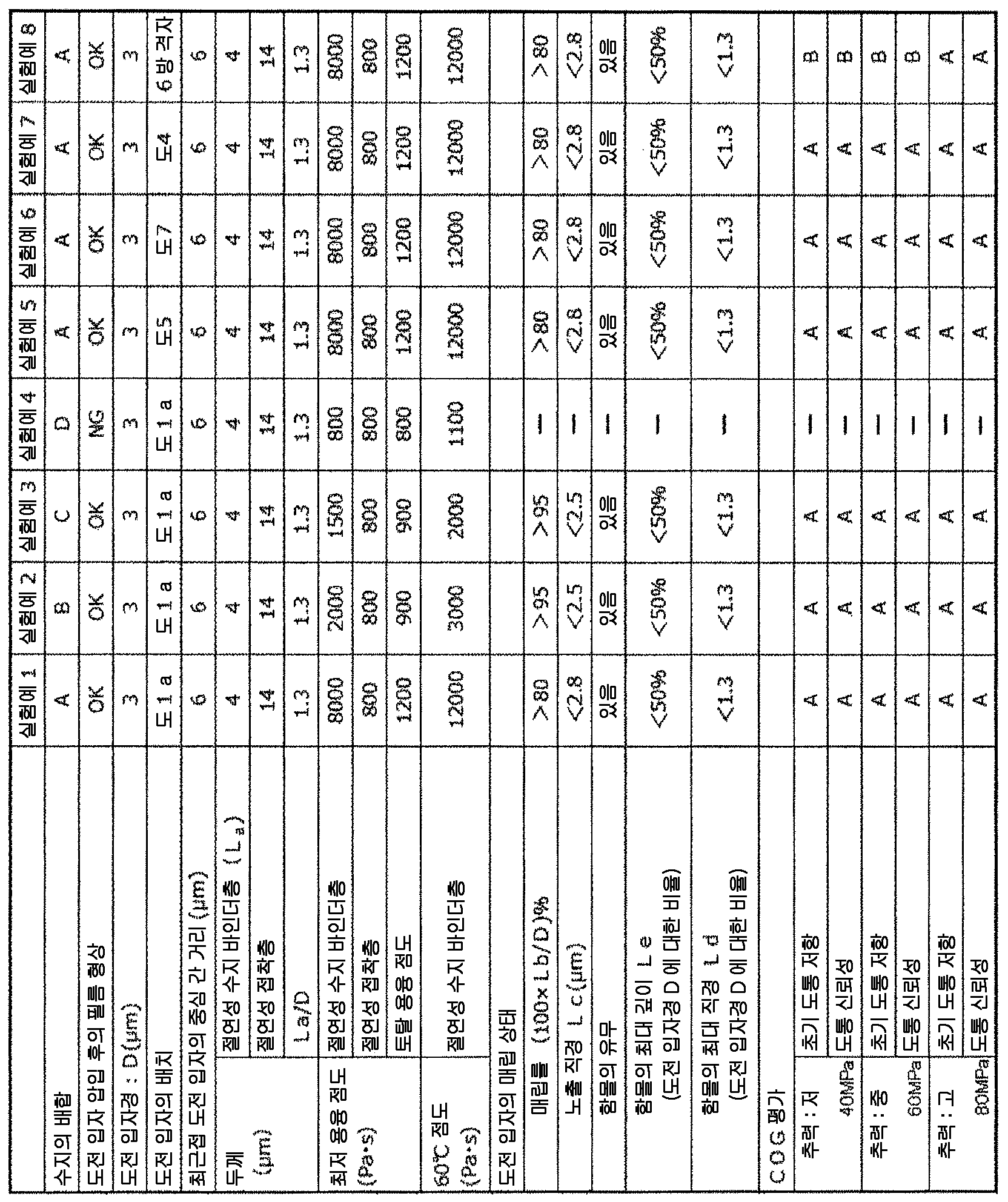
표 2 로부터 절연성 수지 바인더의 최저 용융 점도가 800 Pa·s 인 실험예 4 에서는 도전 입자 근방의 절연성 수지 바인더에 함몰을 갖는 필름의 형성은 어려운 것을 알 수 있다. 한편, 절연성 수지 바인더의 최저 용융 점도가 1500 Pa·s 이상인 실험예에서는, 도전 입자의 매립 시의 조건의 조정에 의해 절연성 수지 바인더의 도전 입자 근방에 볼록부를 형성할 수 있는 것, 이렇게 하여 얻어진 이방성 도전 필름은 COG 용으로 도통 특성이 양호한 것을 알 수 있다. 또, 6 방 격자 배열의 실험예 8 에 비해 도전 입자의 개수 밀도가 낮은 실험예 1 ∼ 7 에서는, 이방성 도전 접속을 보다 저압으로 실시할 수 있는 것을 알 수 있다. It can be seen from Table 2 that in Experimental Example 4 in which the minimum melt viscosity of the insulating resin binder is 800 Pa · s, it is difficult to form a film having a depression in the insulating resin binder near the conductive particles. On the other hand, in the experimental example in which the minimum melting viscosity of the insulating resin binder is 1500 Pa · s or more, it is possible to form convex portions near the conductive particles of the insulating resin binder by adjusting the conditions at the time of embedding the conductive particles, It can be seen that the conductive film has good conduction characteristics for COG. It can also be seen that in Examples 1 to 7 in which the number density of the conductive particles is lower than that in Experimental Example 8 of the hexagonal lattice arrangement, the anisotropic conductive connection can be performed at a lower pressure.
(c) 쇼트율 (c) Short rate
실험예 1 ∼ 3 과 5 ∼ 8 의 이방성 도전 필름을 사용하고, 다음의 쇼트율의 평가용 IC 를 사용하여 180 ℃, 60 MPa, 5 초의 접속 조건으로 평가용 접속물을 얻고, 얻어진 평가용 접속물의 쇼트수를 계측하고, 평가용 IC 의 단자수에 대한 계측한 쇼트수의 비율로서 쇼트율을 구하였다. Using the anisotropic conductive films of Experimental Examples 1 to 3 and 5 to 8, evaluation interconnects were obtained under the connection conditions of 180 DEG C and 60 MPa for 5 seconds using the following evaluation IC for a short rate, The shot number of water was measured, and the shot rate was obtained as the ratio of the number of shots measured to the number of terminals of the evaluation IC.
쇼트율의 평가용 IC (7.5 ㎛ 스페이스의 톱니 TEG (test element group) :Evaluation IC for the short rate (7.5 [micro] m spaced TEG (test element group):
외형 15 × 13 mm Outline 15 × 13 mm
두께 0.5 mm Thickness 0.5 mm
범프 사양 사이즈 25 × 140 ㎛, 범프 간 거리 7.5 ㎛, 범프 높이 15 ㎛ Bump specification size 25 占 140 占 퐉, bump distance 7.5 占 퐉, bump height 15 占 퐉
쇼트는 50 ppm 미만이면 실용상 바람직하고, 실험예 1 ∼ 3 과 5 ∼ 8 의 이방성 도전 필름은 모두 50 ppm 미만이었다. Shots less than 50 ppm were preferable for practical use, and all of the anisotropic conductive films of Experimental Examples 1 to 3 and 5 to 8 were less than 50 ppm.
또한, 실험예 4 를 제외한 각 실험예에 대해, 범프 1 개당에 포착되어 있는 도전 입자를 계측한 바, 모두 10 개 이상의 도전 입자가 포착되어 있었다. For each of the experimental examples except Experimental Example 4, the conductive particles captured per one bump were measured, and all 10 or more conductive particles were trapped.
실험예 9 ∼ 16 Experimental Examples 9 to 16
(이방성 도전 필름의 제작) (Fabrication of anisotropic conductive film)
FOG 접속에 사용하는 이방성 도전 필름에 대해, 절연성 수지 바인더의 수지 조성과 도전 입자의 배치가 필름 형성능과 도통 특성에 미치는 영향을 다음과 같이 하여 조사하였다. The effect of the resin composition of the insulating resin binder and the arrangement of the conductive particles on the film forming ability and the conduction characteristics of the anisotropic conductive film used for the FOG connection was investigated as follows.
즉, 표 3 에 나타낸 배합으로 절연성 수지 바인더와 절연성 접착층을 형성하는 수지 조성물을 조제하고, 이들을 사용하여 실험예 1 과 마찬가지로 하여 이방성 도전 필름을 제작하였다. 이 경우의 도전 입자의 배치와 최근접 입자의 중심 간 거리를 표 4 에 나타낸다. 실험예 16 에서는 도전 입자의 배치를 6 방 격자 배열 (개수 밀도 15000 개/㎟) 로 하고, 그 격자축의 하나를 이방성 도전 필름의 길이 방향에 대해 15°경사지게 하였다. That is, a resin composition for forming an insulating resin binder and an insulating adhesive layer was prepared by the formulation shown in Table 3, and an anisotropic conductive film was produced in the same manner as in Experimental Example 1 by using these. Table 4 shows the arrangement of the conductive particles in this case and the distance between the centers of the nearest neighbor particles. In Experimental Example 16, the conductive particles were arranged in a six-grid arrangement (number density of 15,000 pieces / mm 2), and one of the grid axes was inclined at 15 ° with respect to the longitudinal direction of the anisotropic conductive film.
이 이방성 도전 필름의 제작 공정에 있어서, 절연성 수지 바인더에 도전 입자를 압입한 후에 실험예 12 에서는 필름 형상이 유지되지 않았지만, 그 이외의 실험예에서는 필름 형상이 유지되었다. 그 때문에, 실험예 12 를 제외한 실험예의 이방성 도전 필름에 대해 도전 입자의 매립 상태를 금속 현미경으로 관찰하여 계측하고, 추가로 이후의 평가를 실시하였다. 각 실험예에 있어서의 도전 입자의 매립 상태를 표 4 에 나타낸다. 표 4 에 나타낸 매립 상태는, 표 2 와 마찬가지로 각 실험예마다 절연성 수지 바인더의 함몰이 가장 명확하게 관찰된 것의 계측값이다. In the manufacturing process of the anisotropic conductive film, the film shape was not retained in Experimental Example 12 after the conductive particles were pressed into the insulating resin binder, but in the other experimental examples, the film shape was maintained. Therefore, the embedding state of the conductive particles in the anisotropic conductive film of Experimental Example except Experimental Example 12 was observed with a metallurgical microscope, and further evaluation was carried out thereafter. Table 4 shows the embedding conditions of the conductive particles in each experimental example. The embedding condition shown in Table 4 is a measurement value in which depression of the insulating resin binder is most clearly observed in each of the experimental examples as in Table 2. [
(평가) (evaluation)
각 실험예의 이방성 도전 필름에 대해, 다음과 같이 하여 (a) 초기 도통 저항과 (b) 도통 신뢰성을 측정하였다. 결과를 표 4 에 나타낸다. With respect to the anisotropic conductive films of each experimental example, (a) initial conduction resistance and (b) conduction reliability were measured as follows. The results are shown in Table 4.
(a) 초기 도통 저항 (a) Initial conduction resistance
각 실험예에서 얻은 이방성 도전 필름을 2 mm × 40 mm 로 재단하고, 도통 특성의 평가용 FPC 와 유리 기판 사이에 끼우고, 툴폭 2 mm 로 가열 가압 (180 ℃, 5 초) 하여 각 평가용 접속물을 얻었다. 이 경우, 압박 툴에 의한 추력을 저 (3 MPa), 중 (4.5 MPa), 고 (6 MPa) 의 3 단계로 바꾸어 3 종류의 평가용 접속물을 얻었다. 얻어진 평가용 접속물의 도통 저항을 실험예 1 과 마찬가지로 측정하고, 그 측정값을 다음의 기준으로 3 단계로 평가하였다. The anisotropic conductive film obtained in each Experimental Example was cut into 2 mm x 40 mm, sandwiched between the FPC for evaluation of the conduction characteristics and the glass substrate, heated and pressed (180 DEG C for 5 seconds) with a tool width of 2 mm, Water was obtained. In this case, the thrust by the pressing tool was changed into three stages of low (3 MPa), medium (4.5 MPa) and high (6 MPa) to obtain three kinds of evaluation connecting members. The conduction resistance of the resulting connecting piece was measured in the same manner as in Experimental Example 1, and the measured value was evaluated in three steps based on the following criteria.
평가용 FPC : Evaluation FPC:
단자 피치 20 ㎛
단자 폭/단자 간 스페이스 8.5 ㎛/11.5 ㎛ Terminal width / space between terminals 8.5 탆 / 11.5 탆
폴리이미드 필름 두께 (PI)/구리박 두께 (Cu) = 38/8, Sn plating Polyimide film thickness (PI) / copper foil thickness (Cu) = 38/8, Sn plating
논알칼리 유리 기판 : Non-alkali glass substrate:
전극 ITO 배선 Electrode ITO wiring
두께 0.7 mm Thickness 0.7 mm
초기 도통 저항의 평가 기준 Evaluation Criteria of Initial Conducting Resistance
A : 1.6 Ω 미만 A: less than 1.6 Ω
B : 1.6 Ω 이상 2.0 Ω 미만 B: 1.6 Ω or more and less than 2.0 Ω
C : 2.0 Ω 이상 C: 2.0 Ω or more
(b) 도통 신뢰성 (b) conduction reliability
(a) 에서 제작한 평가용 접속물을, 온도 85 ℃, 습도 85 %RH 의 항온조에 500 시간 두고, 그 후의 도통 저항을 초기 도통 저항과 마찬가지로 측정하고, 그 측정값을 다음의 기준으로 3 단계로 평가하였다. (a) was placed in a thermostatic chamber at a temperature of 85 DEG C and a humidity of 85% RH for 500 hours, and the subsequent conduction resistance was measured in the same manner as the initial conduction resistance, and the measured value was measured in three steps Respectively.
도통 신뢰성의 평가 기준 Criteria for evaluation of continuity reliability
A : 3.0 Ω 미만 A: Less than 3.0 Ω
B : 3.0 Ω 이상 4 Ω 미만 B: 3.0 Ω or more and less than 4 Ω
C : 4.0 Ω 이상 C: 4.0 Ω or more
표 4 로부터 절연성 수지 바인더의 최저 용융 점도가 800 Pa·s 인 실험예 12 에서는, 함몰을 갖는 필름의 형성은 어려운 것을 알 수 있다. 한편, 절연성 수지층의 최저 용융 점도가 1500 Pa·s 이상인 실험예에서는, 도전 입자의 매립 시의 조건의 조정에 의해 절연성 수지 바인더의 도전 입자 근방에 함몰을 형성할 수 있는 것, 이렇게 하여 얻어진 이방성 도전 필름은 FOG 용으로 도통 특성이 양호한 것을 알 수 있다. It can be seen from Table 4 that in Experimental Example 12 in which the insulating resin binder has the lowest melt viscosity of 800 Pa · s, it is difficult to form a film having a depression. On the other hand, in the experimental example in which the minimum melt viscosity of the insulating resin layer is 1500 Pa · s or more, it is possible to form a depression in the vicinity of the conductive particles of the insulating resin binder by adjusting the conditions at the time of embedding the conductive particles, It can be seen that the conductive film has good conduction characteristics for FOG.
(c) 쇼트율 (c) Short rate
초기 도통 저항을 측정한 평가용 접속물의 쇼트수를 계측하고, 계측된 쇼트수와 평가용 접속물의 갭수로부터 쇼트 발생률을 구하였다. 쇼트 발생률은 100 ppm 미만이면 실용상 문제는 없다. The number of shots of the evaluation connection for which the initial conduction resistance was measured was measured, and the rate of shot occurrence was obtained from the measured number of shots and the number of gaps of the evaluation connection. If the shot generation rate is less than 100 ppm, there is no practical problem.
실험예 9 ∼ 11 과 13 ∼ 16 모두 쇼트 발생률은 100 ppm 미만이었다. In Examples 9 to 11 and 13 to 16, the shot generation rate was less than 100 ppm.
또한, 실험예 12 를 제외한 각 실험예에 대해, 범프 1 개당에 포착되어 있는 도전 입자를 계측한 바, 모두 10 개 이상의 도전 입자가 포착되어 있었다. In each of the experimental examples except Experimental Example 12, the conductive particles captured per one bump were measured, and it was found that at least 10 conductive particles were trapped.
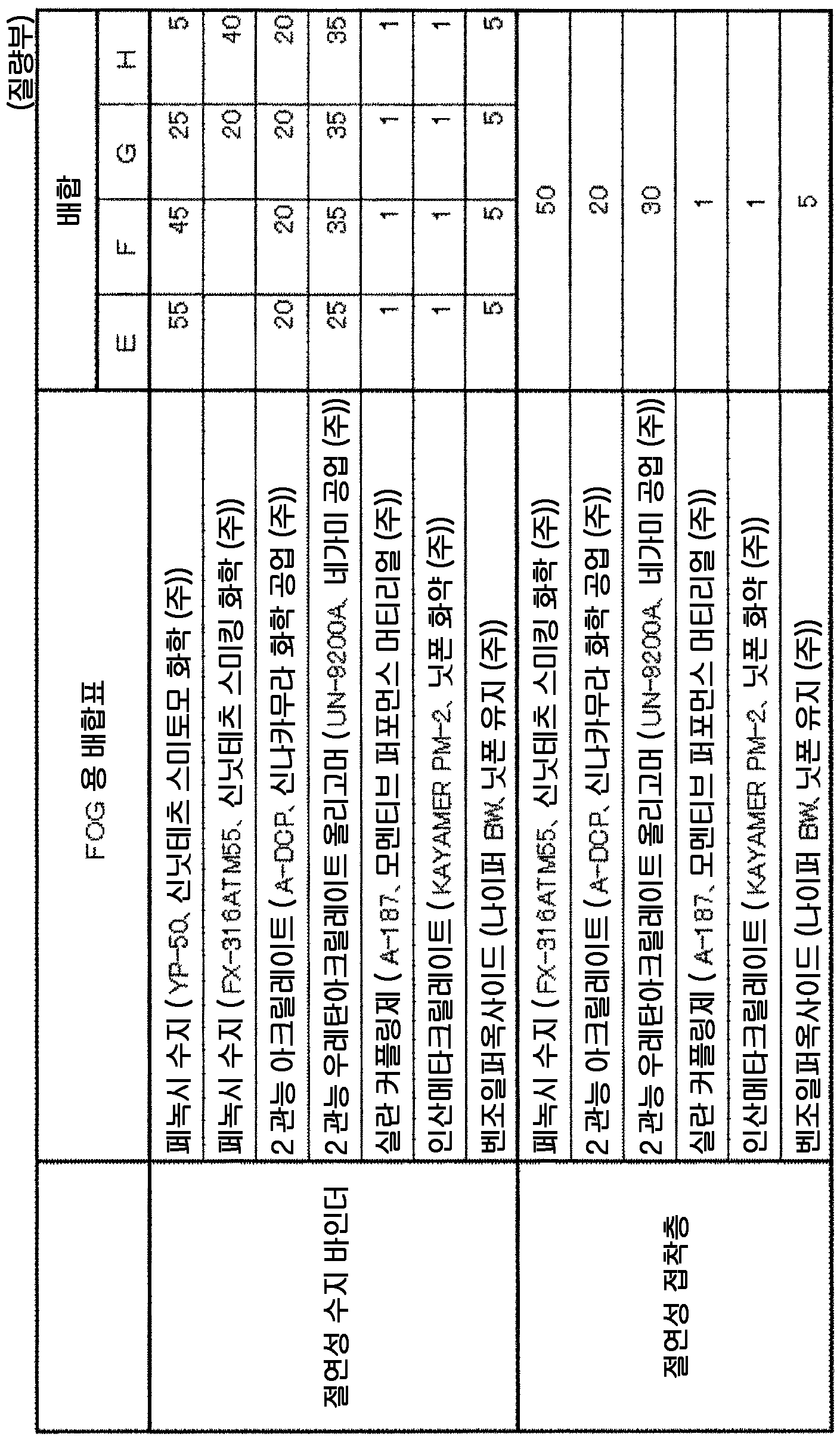

1A, 1B, 1C, 1D, 1E, 1F, 1G, 1H, 1I, 1a, 1b, 1c, 1d, 1e : 이방성 도전 필름
2, 2a, 2b, 2c, 2s : 도전 입자
2m, 2n, 2o, 2p, 2q, 2r : 도전 입자열
2t : 도전 입자의 정부
3 : 절연성 수지 바인더
3a : 절연성 수지 바인더의 표면
3b, 3c : 함몰
3P : 접평면
4 : 절연성 접착층
5, 5B : 반복 유닛
5a : 이방성 도전 필름의 길이 방향과 평행한 변
5b : 이방성 도전 필름의 폭 방향과 평행한 변
5x : 반복 유닛의 외형을 이루는 도전 입자의 중심을 순차 이어 형성되는 다각형
D : 평균 입자경
L1, L2 : 외접선
La : 절연성 수지 바인더의 두께
Lb : 도전 입자의 매립량
Lc : 도전 입자의 노출 부분의 직경
Ld : 함몰의 최대 직경
Le, Lf : 최대 깊이1C, 1D, 1D, 1E, 1F, 1G, 1H, 1I, 1a, 1b, 1c,
2, 2a, 2b, 2c, 2s: conductive particles
2m, 2n, 2o, 2p, 2q, 2r: conductive particle column
2t: the conductive particle
3: Insulating resin binder
3a: Surface of insulating resin binder
3b, 3c: depression
3P: Tangent plane
4: Insulating adhesive layer
5, 5B: Repeat unit
5a: a side parallel to the longitudinal direction of the anisotropic conductive film
5b: a side parallel to the width direction of the anisotropic conductive film
5x: a polygon formed by sequentially forming the centers of the conductive particles constituting the outer shape of the repeating unit
D: average particle size
L1, L2: Outer line
La: thickness of insulating resin binder
Lb: amount of embedded conductive particles
Lc: Diameter of the exposed part of the conductive particle
Ld: Maximum diameter of depression
Le, Lf: maximum depth
Claims (12)
도전 입자가 간격을 두고 일렬로 배열된 도전 입자열로서 도전 입자수가 상이한 것이 병렬하여 이루어지는 도전 입자의 반복 유닛이 반복 배치되어 있는, 이방성 도전 필름. An anisotropic conductive film in which conductive particles are disposed in an insulating resin binder,
Wherein the repeating unit of the conductive particles in which the number of conductive particles is different from that of the conductive particles in a row is arranged repeatedly.
반복 유닛이 이방성 도전 필름의 전체면에 걸쳐서 배치되어 있는, 이방성 도전 필름. The method according to claim 1,
Wherein the repeating unit is disposed over the entire surface of the anisotropic conductive film.
반복 유닛에 있어서 병렬하고 있는 도전 입자열을 구성하는 도전 입자수가 점차 상이한, 이방성 도전 필름.3. The method according to claim 1 or 2,
Wherein the number of conductive particles constituting the parallel conductive column in the repeating unit is gradually different.
반복 유닛에 있어서 병렬하고 있는 3 열의 도전 입자열에 있어서, 중앙의 도전 입자열을 구성하는 도전 입자수가 양측의 도전 입자열을 구성하는 도전 입자수보다 많거나 적은, 이방성 도전 필름.3. The method according to claim 1 or 2,
Wherein the number of conductive particles constituting the center conductive particle row is larger or smaller than the number of conductive particles constituting the conductive particle columns on both sides in the conductive column of three rows arranged in parallel in the repeating unit.
반복 유닛의 외형을 이루는 도전 입자의 중심을 순차 이어 형성되는 다각형의 각 변이 이방성 도전 필름의 길이 방향 또는 폭 방향과 사교하고 있는, 이방성 도전 필름.5. The method according to any one of claims 1 to 4,
Wherein each side of the polygon formed successively from the centers of the conductive particles forming the outer shape of the repeating unit is sagged with the longitudinal direction or the width direction of the anisotropic conductive film.
반복 유닛의 외형을 이루는 도전 입자의 중심을 순차 이어 형성되는 다각형이 이방성 도전 필름의 길이 방향 또는 폭 방향과 평행한 변을 갖는, 이방성 도전 필름. 5. The method according to any one of claims 1 to 4,
Wherein the polygon formed successively at the centers of the conductive particles constituting the outer shape of the repeating unit has a side parallel to the longitudinal direction or the width direction of the anisotropic conductive film.
반복 유닛에 있어서, 도전 입자열끼리가 평행인, 이방성 도전 필름.7. The method according to any one of claims 1 to 6,
Wherein in the repeating unit, the conductive particle columns are parallel to each other.
반복 유닛과 함께 단독의 도전 입자가 반복 배치되어 있는, 이방성 도전 필름.8. The method according to any one of claims 1 to 7,
Wherein the conductive particles are repeatedly arranged together with the repeating unit.
반복 유닛 내에 있어서, 인접하는 도전 입자끼리의 최근접 거리가 도전 입자의 평균 입자경의 0.5 배 이상인, 이방성 도전 필름. 9. The method according to any one of claims 1 to 8,
Wherein the nearest distance between adjacent conductive particles in the repeating unit is at least 0.5 times the average particle diameter of the conductive particles.
반복 유닛을 구성하는 도전 입자가, 6 방 격자 또는 정방 격자의 각 격자점에 도전 입자가 존재하는 배치로부터, 소정의 격자점의 도전 입자를 규칙적으로 제거한 배치인, 이방성 도전 필름.10. The method according to any one of claims 1 to 9,
Wherein the conductive particles constituting the repeating unit are arranged such that conductive particles having a predetermined lattice point are regularly removed from an arrangement in which conductive particles are present at respective lattice points of a hexagonal lattice or a square lattice.
Priority Applications (1)
| Application Number | Priority Date | Filing Date | Title |
|---|---|---|---|
| KR1020217011350A KR102682993B1 (en) | 2016-05-05 | 2017-04-25 | Anisotropic conductive film |
Applications Claiming Priority (5)
| Application Number | Priority Date | Filing Date | Title |
|---|---|---|---|
| JP2016092903 | 2016-05-05 | ||
| JPJP-P-2016-092903 | 2016-05-05 | ||
| JPJP-P-2017-085744 | 2017-04-24 | ||
| JP2017085744A JP7274811B2 (en) | 2016-05-05 | 2017-04-24 | anisotropic conductive film |
| PCT/JP2017/016345 WO2017191781A1 (en) | 2016-05-05 | 2017-04-25 | Anisotropic electroconductive film |
Related Child Applications (1)
| Application Number | Title | Priority Date | Filing Date |
|---|---|---|---|
| KR1020217011350A Division KR102682993B1 (en) | 2016-05-05 | 2017-04-25 | Anisotropic conductive film |
Publications (2)
| Publication Number | Publication Date |
|---|---|
| KR20180098607A true KR20180098607A (en) | 2018-09-04 |
| KR102243340B1 KR102243340B1 (en) | 2021-04-22 |
Family
ID=60322404
Family Applications (1)
| Application Number | Title | Priority Date | Filing Date |
|---|---|---|---|
| KR1020187021398A Active KR102243340B1 (en) | 2016-05-05 | 2017-04-25 | Anisotropic conductive film |
Country Status (4)
| Country | Link |
|---|---|
| US (1) | US11794444B2 (en) |
| JP (1) | JP7274811B2 (en) |
| KR (1) | KR102243340B1 (en) |
| CN (1) | CN109074894B (en) |
Cited By (2)
| Publication number | Priority date | Publication date | Assignee | Title |
|---|---|---|---|---|
| KR20180098356A (en) * | 2016-05-05 | 2018-09-03 | 데쿠세리아루즈 가부시키가이샤 | Anisotropic conductive film |
| KR20180098355A (en) * | 2016-05-05 | 2018-09-03 | 데쿠세리아루즈 가부시키가이샤 | Anisotropic conductive film |
Families Citing this family (8)
| Publication number | Priority date | Publication date | Assignee | Title |
|---|---|---|---|---|
| WO2017191772A1 (en) * | 2016-05-05 | 2017-11-09 | デクセリアルズ株式会社 | Filler alignment film |
| US12550783B2 (en) | 2016-05-17 | 2026-02-10 | Taiwan Semiconductor Manufacturing Company, Ltd. | Device and method for UBM/RDL routing |
| KR102519126B1 (en) * | 2018-03-30 | 2023-04-06 | 삼성디스플레이 주식회사 | Display device |
| CN112292430A (en) * | 2018-06-06 | 2021-01-29 | 迪睿合株式会社 | Filled membranes |
| CN112534650B (en) | 2018-08-08 | 2023-05-23 | 迪睿合株式会社 | Anisotropic conductive film |
| KR102608245B1 (en) * | 2019-01-21 | 2023-11-29 | 삼성전자주식회사 | Elctrically conductive hybrid membrane, making method thereof, secondary battery and electronic device comprising the same |
| WO2021161935A1 (en) | 2020-02-12 | 2021-08-19 | デクセリアルズ株式会社 | Anisotropic electroconductive film |
| JP2023117329A (en) | 2022-02-10 | 2023-08-23 | デクセリアルズ株式会社 | Conductive film design method |
Citations (8)
| Publication number | Priority date | Publication date | Assignee | Title |
|---|---|---|---|---|
| JPH09320345A (en) | 1996-05-31 | 1997-12-12 | Whitaker Corp:The | Anisotropic conductive film |
| JP2002519473A (en) | 1998-06-30 | 2002-07-02 | ミネソタ マイニング アンド マニュファクチャリング カンパニー | Fine pitch anisotropic conductive adhesive |
| KR20080009043A (en) * | 2004-11-09 | 2008-01-24 | 보드 오브 리전츠, 더 유니버시티 오브 텍사스 시스템 | Manufacturing and Applications of Nanofiber Ribbons and Sheets and Twisted and Non-Twisted Nanofiber Spinning Yarns |
| JP2009076431A (en) * | 2007-01-31 | 2009-04-09 | Tokai Rubber Ind Ltd | Anisotropic conductive film and method for producing the same |
| JP4887700B2 (en) | 2005-09-09 | 2012-02-29 | 住友ベークライト株式会社 | Anisotropic conductive film and electronic / electrical equipment |
| JP2014063729A (en) * | 2012-08-29 | 2014-04-10 | Dexerials Corp | Anisotropic conductive film and method for producing the same |
| JP2016015205A (en) * | 2014-06-30 | 2016-01-28 | デクセリアルズ株式会社 | Anisotropic conductive film and connection structure |
| KR20170113039A (en) * | 2016-03-25 | 2017-10-12 | 데쿠세리아루즈 가부시키가이샤 | Electronic component, connection structure, method for designing electronic component |
Family Cites Families (15)
| Publication number | Priority date | Publication date | Assignee | Title |
|---|---|---|---|---|
| US4209481A (en) | 1976-04-19 | 1980-06-24 | Toray Industries, Inc. | Process for producing an anisotropically electroconductive sheet |
| JPS6032282B2 (en) | 1976-09-09 | 1985-07-27 | 東レ株式会社 | Anisotropic conductive sheet and method for manufacturing the same |
| JPH0461398A (en) | 1990-06-29 | 1992-02-27 | Mitsubishi Kasei Corp | Interlaminar circuit connection method |
| JP5388572B2 (en) * | 2006-04-27 | 2014-01-15 | デクセリアルズ株式会社 | Conductive particle arrangement sheet and anisotropic conductive film |
| JP2007019550A (en) | 2006-10-06 | 2007-01-25 | Seiko Epson Corp | Manufacturing method of electronic device |
| JP2010019672A (en) | 2008-07-10 | 2010-01-28 | Sumitomo Electric Ind Ltd | Substrate body |
| JP2010251337A (en) | 2010-08-05 | 2010-11-04 | Sony Chemical & Information Device Corp | Anisotropic conductive film, method for manufacturing the same and connection structure |
| JP5757801B2 (en) * | 2011-06-29 | 2015-08-05 | 根泰 許 | burner |
| KR20170044766A (en) * | 2012-08-01 | 2017-04-25 | 데쿠세리아루즈 가부시키가이샤 | Method for manufacturing anisotropically conductive film, anisotropically conductive film, and connective structure |
| JP2015032500A (en) | 2013-08-05 | 2015-02-16 | 株式会社クラレ | Anisotropic conductor film, manufacturing method thereof, device, electron emission element, field emission lamp, and field emission display |
| JP2015079586A (en) | 2013-10-15 | 2015-04-23 | デクセリアルズ株式会社 | Anisotropic conductive film |
| JP6119718B2 (en) | 2013-11-19 | 2017-04-26 | デクセリアルズ株式会社 | Anisotropic conductive film and connection structure |
| JP6661888B2 (en) | 2014-03-31 | 2020-03-11 | デクセリアルズ株式会社 | Method for producing anisotropic conductive film |
| JP2015232660A (en) | 2014-06-10 | 2015-12-24 | 株式会社Joled | Display device manufacturing method and display device |
| JP6661969B2 (en) | 2014-10-28 | 2020-03-11 | デクセリアルズ株式会社 | Anisotropic conductive film and connection structure |
-
2017
- 2017-04-24 JP JP2017085744A patent/JP7274811B2/en active Active
- 2017-04-25 CN CN201780025115.8A patent/CN109074894B/en active Active
- 2017-04-25 US US16/085,515 patent/US11794444B2/en active Active
- 2017-04-25 KR KR1020187021398A patent/KR102243340B1/en active Active
Patent Citations (8)
| Publication number | Priority date | Publication date | Assignee | Title |
|---|---|---|---|---|
| JPH09320345A (en) | 1996-05-31 | 1997-12-12 | Whitaker Corp:The | Anisotropic conductive film |
| JP2002519473A (en) | 1998-06-30 | 2002-07-02 | ミネソタ マイニング アンド マニュファクチャリング カンパニー | Fine pitch anisotropic conductive adhesive |
| KR20080009043A (en) * | 2004-11-09 | 2008-01-24 | 보드 오브 리전츠, 더 유니버시티 오브 텍사스 시스템 | Manufacturing and Applications of Nanofiber Ribbons and Sheets and Twisted and Non-Twisted Nanofiber Spinning Yarns |
| JP4887700B2 (en) | 2005-09-09 | 2012-02-29 | 住友ベークライト株式会社 | Anisotropic conductive film and electronic / electrical equipment |
| JP2009076431A (en) * | 2007-01-31 | 2009-04-09 | Tokai Rubber Ind Ltd | Anisotropic conductive film and method for producing the same |
| JP2014063729A (en) * | 2012-08-29 | 2014-04-10 | Dexerials Corp | Anisotropic conductive film and method for producing the same |
| JP2016015205A (en) * | 2014-06-30 | 2016-01-28 | デクセリアルズ株式会社 | Anisotropic conductive film and connection structure |
| KR20170113039A (en) * | 2016-03-25 | 2017-10-12 | 데쿠세리아루즈 가부시키가이샤 | Electronic component, connection structure, method for designing electronic component |
Cited By (5)
| Publication number | Priority date | Publication date | Assignee | Title |
|---|---|---|---|---|
| KR20180098356A (en) * | 2016-05-05 | 2018-09-03 | 데쿠세리아루즈 가부시키가이샤 | Anisotropic conductive film |
| KR20180098355A (en) * | 2016-05-05 | 2018-09-03 | 데쿠세리아루즈 가부시키가이샤 | Anisotropic conductive film |
| KR20200103874A (en) * | 2016-05-05 | 2020-09-02 | 데쿠세리아루즈 가부시키가이샤 | Anisotropic conductive film |
| KR20210122900A (en) * | 2016-05-05 | 2021-10-12 | 데쿠세리아루즈 가부시키가이샤 | Anisotropic conductive film |
| KR20230030025A (en) * | 2016-05-05 | 2023-03-03 | 데쿠세리아루즈 가부시키가이샤 | Anisotropic conductive film |
Also Published As
| Publication number | Publication date |
|---|---|
| US20190035763A1 (en) | 2019-01-31 |
| JP7274811B2 (en) | 2023-05-17 |
| JP2017204463A (en) | 2017-11-16 |
| US11794444B2 (en) | 2023-10-24 |
| KR102243340B1 (en) | 2021-04-22 |
| CN109074894B (en) | 2021-07-30 |
| CN109074894A (en) | 2018-12-21 |
Similar Documents
| Publication | Publication Date | Title |
|---|---|---|
| KR20180098607A (en) | Anisotropic conductive film | |
| KR102228112B1 (en) | Anisotropic conductive film | |
| KR102011650B1 (en) | Anisotropic conductive film and connection structure | |
| KR20180098356A (en) | Anisotropic conductive film | |
| KR102314818B1 (en) | Filler-containing film | |
| JP7401798B2 (en) | Anisotropic conductive film | |
| KR102240767B1 (en) | Method of producing anisotropic conductive film | |
| JP7607603B2 (en) | Anisotropic Conductive Film | |
| KR102423362B1 (en) | Connection structure | |
| KR20190064644A (en) | Anisotropic conductive film | |
| HK40064112A (en) | Anisotropic conductive film | |
| HK1261541A1 (en) | Anisotropic electroconductive film | |
| HK1261541B (en) | Anisotropic electroconductive film | |
| HK40001200A (en) | Anisotropic conductive film | |
| HK40001200B (en) | Anisotropic conductive film |
Legal Events
| Date | Code | Title | Description |
|---|---|---|---|
| A201 | Request for examination | ||
| AMND | Amendment | ||
| P11-X000 | Amendment of application requested |
St.27 status event code: A-2-2-P10-P11-nap-X000 |
|
| P13-X000 | Application amended |
St.27 status event code: A-2-2-P10-P13-nap-X000 |
|
| PA0105 | International application |
St.27 status event code: A-0-1-A10-A15-nap-PA0105 |
|
| PA0201 | Request for examination |
St.27 status event code: A-1-2-D10-D11-exm-PA0201 |
|
| PG1501 | Laying open of application |
St.27 status event code: A-1-1-Q10-Q12-nap-PG1501 |
|
| E902 | Notification of reason for refusal | ||
| PE0902 | Notice of grounds for rejection |
St.27 status event code: A-1-2-D10-D21-exm-PE0902 |
|
| E601 | Decision to refuse application | ||
| PE0601 | Decision on rejection of patent |
St.27 status event code: N-2-6-B10-B15-exm-PE0601 |
|
| X091 | Application refused [patent] | ||
| AMND | Amendment | ||
| P11-X000 | Amendment of application requested |
St.27 status event code: A-2-2-P10-P11-nap-X000 |
|
| P13-X000 | Application amended |
St.27 status event code: A-2-2-P10-P13-nap-X000 |
|
| PX0901 | Re-examination |
St.27 status event code: A-2-3-E10-E12-rex-PX0901 |
|
| E902 | Notification of reason for refusal | ||
| PE0902 | Notice of grounds for rejection |
St.27 status event code: A-1-2-D10-D21-exm-PE0902 |
|
| T11-X000 | Administrative time limit extension requested |
St.27 status event code: U-3-3-T10-T11-oth-X000 |
|
| T11-X000 | Administrative time limit extension requested |
St.27 status event code: U-3-3-T10-T11-oth-X000 |
|
| T11-X000 | Administrative time limit extension requested |
St.27 status event code: U-3-3-T10-T11-oth-X000 |
|
| AMND | Amendment | ||
| P11-X000 | Amendment of application requested |
St.27 status event code: A-2-2-P10-P11-nap-X000 |
|
| P13-X000 | Application amended |
St.27 status event code: A-2-2-P10-P13-nap-X000 |
|
| PX0701 | Decision of registration after re-examination |
St.27 status event code: A-3-4-F10-F13-rex-PX0701 |
|
| X701 | Decision to grant (after re-examination) | ||
| A107 | Divisional application of patent | ||
| GRNT | Written decision to grant | ||
| PA0104 | Divisional application for international application |
St.27 status event code: A-0-1-A10-A18-div-PA0104 St.27 status event code: A-0-1-A10-A16-div-PA0104 |
|
| PR0701 | Registration of establishment |
St.27 status event code: A-2-4-F10-F11-exm-PR0701 |
|
| PR1002 | Payment of registration fee |
St.27 status event code: A-2-2-U10-U12-oth-PR1002 Fee payment year number: 1 |
|
| PG1601 | Publication of registration |
St.27 status event code: A-4-4-Q10-Q13-nap-PG1601 |
|
| R18-X000 | Changes to party contact information recorded |
St.27 status event code: A-5-5-R10-R18-oth-X000 |
|
| PR1001 | Payment of annual fee |
St.27 status event code: A-4-4-U10-U11-oth-PR1001 Fee payment year number: 4 |
|
| PR1001 | Payment of annual fee |
St.27 status event code: A-4-4-U10-U11-oth-PR1001 Fee payment year number: 5 |
|
| U11 | Full renewal or maintenance fee paid |
Free format text: ST27 STATUS EVENT CODE: A-4-4-U10-U11-OTH-PR1001 (AS PROVIDED BY THE NATIONAL OFFICE) Year of fee payment: 5 |