KR20120003495A - Led용 클러스터 툴 - Google Patents
Led용 클러스터 툴 Download PDFInfo
- Publication number
- KR20120003495A KR20120003495A KR1020117028399A KR20117028399A KR20120003495A KR 20120003495 A KR20120003495 A KR 20120003495A KR 1020117028399 A KR1020117028399 A KR 1020117028399A KR 20117028399 A KR20117028399 A KR 20117028399A KR 20120003495 A KR20120003495 A KR 20120003495A
- Authority
- KR
- South Korea
- Prior art keywords
- chamber
- substrates
- processing chamber
- layer
- mocvd
- Prior art date
- Legal status (The legal status is an assumption and is not a legal conclusion. Google has not performed a legal analysis and makes no representation as to the accuracy of the status listed.)
- Ceased
Links
- 239000000758 substrate Substances 0.000 claims abstract description 254
- 238000012545 processing Methods 0.000 claims abstract description 236
- 238000000034 method Methods 0.000 claims abstract description 125
- 230000008569 process Effects 0.000 claims abstract description 96
- IJGRMHOSHXDMSA-UHFFFAOYSA-N Atomic nitrogen Chemical compound N#N IJGRMHOSHXDMSA-UHFFFAOYSA-N 0.000 claims abstract description 76
- 229910052757 nitrogen Inorganic materials 0.000 claims abstract description 38
- 238000004519 manufacturing process Methods 0.000 claims abstract description 37
- 229910052751 metal Inorganic materials 0.000 claims abstract description 14
- 239000002184 metal Substances 0.000 claims abstract description 14
- 238000005229 chemical vapour deposition Methods 0.000 claims abstract description 5
- 150000004678 hydrides Chemical class 0.000 claims abstract description 3
- 239000012808 vapor phase Substances 0.000 claims abstract description 3
- 239000007789 gas Substances 0.000 claims description 177
- 239000002243 precursor Substances 0.000 claims description 168
- 229910002601 GaN Inorganic materials 0.000 claims description 92
- JMASRVWKEDWRBT-UHFFFAOYSA-N Gallium nitride Chemical compound [Ga]#N JMASRVWKEDWRBT-UHFFFAOYSA-N 0.000 claims description 74
- 238000000151 deposition Methods 0.000 claims description 55
- 238000004140 cleaning Methods 0.000 claims description 47
- QJGQUHMNIGDVPM-UHFFFAOYSA-N nitrogen group Chemical group [N] QJGQUHMNIGDVPM-UHFFFAOYSA-N 0.000 claims description 39
- 239000000460 chlorine Substances 0.000 claims description 35
- 238000012546 transfer Methods 0.000 claims description 34
- ZAMOUSCENKQFHK-UHFFFAOYSA-N Chlorine atom Chemical compound [Cl] ZAMOUSCENKQFHK-UHFFFAOYSA-N 0.000 claims description 33
- 229910052801 chlorine Inorganic materials 0.000 claims description 33
- -1 compound nitride Chemical class 0.000 claims description 32
- 229910052733 gallium Inorganic materials 0.000 claims description 32
- GYHNNYVSQQEPJS-UHFFFAOYSA-N Gallium Chemical compound [Ga] GYHNNYVSQQEPJS-UHFFFAOYSA-N 0.000 claims description 30
- 239000004065 semiconductor Substances 0.000 claims description 28
- 229910002704 AlGaN Inorganic materials 0.000 claims description 26
- 239000012298 atmosphere Substances 0.000 claims description 15
- 238000002230 thermal chemical vapour deposition Methods 0.000 claims description 13
- 229910052782 aluminium Inorganic materials 0.000 claims description 12
- XAGFODPZIPBFFR-UHFFFAOYSA-N aluminium Chemical compound [Al] XAGFODPZIPBFFR-UHFFFAOYSA-N 0.000 claims description 11
- 239000002019 doping agent Substances 0.000 claims description 9
- 229910052738 indium Inorganic materials 0.000 claims description 9
- APFVFJFRJDLVQX-UHFFFAOYSA-N indium atom Chemical compound [In] APFVFJFRJDLVQX-UHFFFAOYSA-N 0.000 claims description 8
- 229910052736 halogen Inorganic materials 0.000 claims description 7
- 150000002367 halogens Chemical class 0.000 claims description 7
- 239000011737 fluorine Substances 0.000 claims description 6
- 229910052731 fluorine Inorganic materials 0.000 claims description 6
- 239000011261 inert gas Substances 0.000 claims description 6
- 229910052794 bromium Inorganic materials 0.000 claims description 4
- WKBOTKDWSSQWDR-UHFFFAOYSA-N Bromine atom Chemical compound [Br] WKBOTKDWSSQWDR-UHFFFAOYSA-N 0.000 claims description 3
- GDTBXPJZTBHREO-UHFFFAOYSA-N bromine Substances BrBr GDTBXPJZTBHREO-UHFFFAOYSA-N 0.000 claims description 3
- PNDPGZBMCMUPRI-UHFFFAOYSA-N iodine Chemical compound II PNDPGZBMCMUPRI-UHFFFAOYSA-N 0.000 claims description 2
- PXGOKWXKJXAPGV-UHFFFAOYSA-N Fluorine Chemical compound FF PXGOKWXKJXAPGV-UHFFFAOYSA-N 0.000 claims 1
- 230000008021 deposition Effects 0.000 description 36
- 239000012530 fluid Substances 0.000 description 26
- QGZKDVFQNNGYKY-UHFFFAOYSA-N Ammonia Chemical compound N QGZKDVFQNNGYKY-UHFFFAOYSA-N 0.000 description 24
- 239000000463 material Substances 0.000 description 17
- 150000004767 nitrides Chemical class 0.000 description 17
- 238000010438 heat treatment Methods 0.000 description 14
- VEXZGXHMUGYJMC-UHFFFAOYSA-M Chloride anion Chemical compound [Cl-] VEXZGXHMUGYJMC-UHFFFAOYSA-M 0.000 description 13
- 229910021529 ammonia Inorganic materials 0.000 description 12
- 239000012159 carrier gas Substances 0.000 description 10
- 238000005137 deposition process Methods 0.000 description 10
- 238000005530 etching Methods 0.000 description 10
- 239000007795 chemical reaction product Substances 0.000 description 9
- 229910052594 sapphire Inorganic materials 0.000 description 9
- 239000010980 sapphire Substances 0.000 description 9
- XKRFYHLGVUSROY-UHFFFAOYSA-N Argon Chemical compound [Ar] XKRFYHLGVUSROY-UHFFFAOYSA-N 0.000 description 8
- VEXZGXHMUGYJMC-UHFFFAOYSA-N Hydrochloric acid Chemical compound Cl VEXZGXHMUGYJMC-UHFFFAOYSA-N 0.000 description 8
- 239000011777 magnesium Substances 0.000 description 8
- 230000015572 biosynthetic process Effects 0.000 description 7
- 238000010586 diagram Methods 0.000 description 7
- 239000000203 mixture Substances 0.000 description 7
- PMHQVHHXPFUNSP-UHFFFAOYSA-M copper(1+);methylsulfanylmethane;bromide Chemical compound Br[Cu].CSC PMHQVHHXPFUNSP-UHFFFAOYSA-M 0.000 description 6
- 238000009826 distribution Methods 0.000 description 6
- 229910052734 helium Inorganic materials 0.000 description 6
- 239000001307 helium Substances 0.000 description 6
- SWQJXJOGLNCZEY-UHFFFAOYSA-N helium atom Chemical compound [He] SWQJXJOGLNCZEY-UHFFFAOYSA-N 0.000 description 6
- 239000007788 liquid Substances 0.000 description 6
- 239000010453 quartz Substances 0.000 description 6
- HBMJWWWQQXIZIP-UHFFFAOYSA-N silicon carbide Chemical compound [Si+]#[C-] HBMJWWWQQXIZIP-UHFFFAOYSA-N 0.000 description 6
- VYPSYNLAJGMNEJ-UHFFFAOYSA-N silicon dioxide Inorganic materials O=[Si]=O VYPSYNLAJGMNEJ-UHFFFAOYSA-N 0.000 description 6
- YCKRFDGAMUMZLT-UHFFFAOYSA-N Fluorine atom Chemical compound [F] YCKRFDGAMUMZLT-UHFFFAOYSA-N 0.000 description 5
- 239000001257 hydrogen Substances 0.000 description 5
- 229910052739 hydrogen Inorganic materials 0.000 description 5
- 150000002431 hydrogen Chemical class 0.000 description 5
- TWNQGVIAIRXVLR-UHFFFAOYSA-N oxo(oxoalumanyloxy)alumane Chemical compound O=[Al]O[Al]=O TWNQGVIAIRXVLR-UHFFFAOYSA-N 0.000 description 5
- 229910010271 silicon carbide Inorganic materials 0.000 description 5
- 238000001228 spectrum Methods 0.000 description 5
- 238000003860 storage Methods 0.000 description 5
- KZBUYRJDOAKODT-UHFFFAOYSA-N Chlorine Chemical compound ClCl KZBUYRJDOAKODT-UHFFFAOYSA-N 0.000 description 4
- PXHVJJICTQNCMI-UHFFFAOYSA-N Nickel Chemical compound [Ni] PXHVJJICTQNCMI-UHFFFAOYSA-N 0.000 description 4
- 229910052786 argon Inorganic materials 0.000 description 4
- 238000004891 communication Methods 0.000 description 4
- 230000000694 effects Effects 0.000 description 4
- 238000011065 in-situ storage Methods 0.000 description 4
- 238000004020 luminiscence type Methods 0.000 description 4
- 229910052749 magnesium Inorganic materials 0.000 description 4
- XLYOFNOQVPJJNP-UHFFFAOYSA-N water Substances O XLYOFNOQVPJJNP-UHFFFAOYSA-N 0.000 description 4
- OKTJSMMVPCPJKN-UHFFFAOYSA-N Carbon Chemical compound [C] OKTJSMMVPCPJKN-UHFFFAOYSA-N 0.000 description 3
- LYCAIKOWRPUZTN-UHFFFAOYSA-N Ethylene glycol Chemical compound OCCO LYCAIKOWRPUZTN-UHFFFAOYSA-N 0.000 description 3
- XUIMIQQOPSSXEZ-UHFFFAOYSA-N Silicon Chemical compound [Si] XUIMIQQOPSSXEZ-UHFFFAOYSA-N 0.000 description 3
- QVGXLLKOCUKJST-UHFFFAOYSA-N atomic oxygen Chemical compound [O] QVGXLLKOCUKJST-UHFFFAOYSA-N 0.000 description 3
- 230000004888 barrier function Effects 0.000 description 3
- 238000005253 cladding Methods 0.000 description 3
- 238000011161 development Methods 0.000 description 3
- 230000018109 developmental process Effects 0.000 description 3
- 229910001873 dinitrogen Inorganic materials 0.000 description 3
- 229910052754 neon Inorganic materials 0.000 description 3
- GKAOGPIIYCISHV-UHFFFAOYSA-N neon atom Chemical compound [Ne] GKAOGPIIYCISHV-UHFFFAOYSA-N 0.000 description 3
- 239000001301 oxygen Substances 0.000 description 3
- 229910052760 oxygen Inorganic materials 0.000 description 3
- 239000000047 product Substances 0.000 description 3
- 238000010926 purge Methods 0.000 description 3
- 230000009257 reactivity Effects 0.000 description 3
- 239000010703 silicon Substances 0.000 description 3
- 239000007787 solid Substances 0.000 description 3
- 241000894007 species Species 0.000 description 3
- 238000002207 thermal evaporation Methods 0.000 description 3
- XCZXGTMEAKBVPV-UHFFFAOYSA-N trimethylgallium Chemical compound C[Ga](C)C XCZXGTMEAKBVPV-UHFFFAOYSA-N 0.000 description 3
- 229910052724 xenon Inorganic materials 0.000 description 3
- FHNFHKCVQCLJFQ-UHFFFAOYSA-N xenon atom Chemical compound [Xe] FHNFHKCVQCLJFQ-UHFFFAOYSA-N 0.000 description 3
- OAKJQQAXSVQMHS-UHFFFAOYSA-N Hydrazine Chemical compound NN OAKJQQAXSVQMHS-UHFFFAOYSA-N 0.000 description 2
- FYYHWMGAXLPEAU-UHFFFAOYSA-N Magnesium Chemical compound [Mg] FYYHWMGAXLPEAU-UHFFFAOYSA-N 0.000 description 2
- GQPLMRYTRLFLPF-UHFFFAOYSA-N Nitrous Oxide Chemical compound [O-][N+]#N GQPLMRYTRLFLPF-UHFFFAOYSA-N 0.000 description 2
- 229910045601 alloy Inorganic materials 0.000 description 2
- 239000000956 alloy Substances 0.000 description 2
- 229910052799 carbon Inorganic materials 0.000 description 2
- 230000015556 catabolic process Effects 0.000 description 2
- 230000008859 change Effects 0.000 description 2
- 238000006243 chemical reaction Methods 0.000 description 2
- 150000001875 compounds Chemical class 0.000 description 2
- 230000001143 conditioned effect Effects 0.000 description 2
- 230000007547 defect Effects 0.000 description 2
- 238000006731 degradation reaction Methods 0.000 description 2
- 239000012535 impurity Substances 0.000 description 2
- 229910052740 iodine Inorganic materials 0.000 description 2
- 230000007246 mechanism Effects 0.000 description 2
- 229910001510 metal chloride Inorganic materials 0.000 description 2
- 229910001507 metal halide Inorganic materials 0.000 description 2
- 150000005309 metal halides Chemical class 0.000 description 2
- 150000002739 metals Chemical class 0.000 description 2
- 238000002156 mixing Methods 0.000 description 2
- 229910052759 nickel Inorganic materials 0.000 description 2
- 239000012299 nitrogen atmosphere Substances 0.000 description 2
- 230000003287 optical effect Effects 0.000 description 2
- 230000005855 radiation Effects 0.000 description 2
- 229910052710 silicon Inorganic materials 0.000 description 2
- JLTRXTDYQLMHGR-UHFFFAOYSA-N trimethylaluminium Chemical compound C[Al](C)C JLTRXTDYQLMHGR-UHFFFAOYSA-N 0.000 description 2
- IBEFSUTVZWZJEL-UHFFFAOYSA-N trimethylindium Chemical compound C[In](C)C IBEFSUTVZWZJEL-UHFFFAOYSA-N 0.000 description 2
- ZCYVEMRRCGMTRW-UHFFFAOYSA-N 7553-56-2 Chemical compound [I] ZCYVEMRRCGMTRW-UHFFFAOYSA-N 0.000 description 1
- PIGFYZPCRLYGLF-UHFFFAOYSA-N Aluminum nitride Chemical compound [Al]#N PIGFYZPCRLYGLF-UHFFFAOYSA-N 0.000 description 1
- 229910000807 Ga alloy Inorganic materials 0.000 description 1
- 229910001218 Gallium arsenide Inorganic materials 0.000 description 1
- 241000243251 Hydra Species 0.000 description 1
- OAICVXFJPJFONN-UHFFFAOYSA-N Phosphorus Chemical compound [P] OAICVXFJPJFONN-UHFFFAOYSA-N 0.000 description 1
- 229910052581 Si3N4 Inorganic materials 0.000 description 1
- BLRPTPMANUNPDV-UHFFFAOYSA-N Silane Chemical compound [SiH4] BLRPTPMANUNPDV-UHFFFAOYSA-N 0.000 description 1
- USZGMDQWECZTIQ-UHFFFAOYSA-N [Mg](C1C=CC=C1)C1C=CC=C1 Chemical compound [Mg](C1C=CC=C1)C1C=CC=C1 USZGMDQWECZTIQ-UHFFFAOYSA-N 0.000 description 1
- 239000002253 acid Substances 0.000 description 1
- 230000002411 adverse Effects 0.000 description 1
- NWAIGJYBQQYSPW-UHFFFAOYSA-N azanylidyneindigane Chemical compound [In]#N NWAIGJYBQQYSPW-UHFFFAOYSA-N 0.000 description 1
- 238000010923 batch production Methods 0.000 description 1
- 230000009286 beneficial effect Effects 0.000 description 1
- 238000007664 blowing Methods 0.000 description 1
- 238000009835 boiling Methods 0.000 description 1
- 239000000969 carrier Substances 0.000 description 1
- 239000003054 catalyst Substances 0.000 description 1
- 150000001805 chlorine compounds Chemical class 0.000 description 1
- XOYLJNJLGBYDTH-UHFFFAOYSA-M chlorogallium Chemical compound [Ga]Cl XOYLJNJLGBYDTH-UHFFFAOYSA-M 0.000 description 1
- 239000002131 composite material Substances 0.000 description 1
- 239000012141 concentrate Substances 0.000 description 1
- 239000000356 contaminant Substances 0.000 description 1
- 238000001816 cooling Methods 0.000 description 1
- 230000007797 corrosion Effects 0.000 description 1
- 238000005260 corrosion Methods 0.000 description 1
- RAABOESOVLLHRU-UHFFFAOYSA-N diazene Chemical compound N=N RAABOESOVLLHRU-UHFFFAOYSA-N 0.000 description 1
- PZPGRFITIJYNEJ-UHFFFAOYSA-N disilane Chemical compound [SiH3][SiH3] PZPGRFITIJYNEJ-UHFFFAOYSA-N 0.000 description 1
- 239000006185 dispersion Substances 0.000 description 1
- 230000009977 dual effect Effects 0.000 description 1
- 239000012636 effector Substances 0.000 description 1
- 230000005496 eutectics Effects 0.000 description 1
- UPWPDUACHOATKO-UHFFFAOYSA-K gallium trichloride Chemical compound Cl[Ga](Cl)Cl UPWPDUACHOATKO-UHFFFAOYSA-K 0.000 description 1
- 239000011521 glass Substances 0.000 description 1
- 229910002804 graphite Inorganic materials 0.000 description 1
- 239000010439 graphite Substances 0.000 description 1
- 150000004820 halides Chemical class 0.000 description 1
- 229910000856 hastalloy Inorganic materials 0.000 description 1
- 229910001026 inconel Inorganic materials 0.000 description 1
- 238000002347 injection Methods 0.000 description 1
- 239000007924 injection Substances 0.000 description 1
- 238000003780 insertion Methods 0.000 description 1
- 230000037431 insertion Effects 0.000 description 1
- 239000011630 iodine Substances 0.000 description 1
- QRXWMOHMRWLFEY-UHFFFAOYSA-N isoniazide Chemical compound NNC(=O)C1=CC=NC=C1 QRXWMOHMRWLFEY-UHFFFAOYSA-N 0.000 description 1
- 229910001338 liquidmetal Inorganic materials 0.000 description 1
- MNKMDLVKGZBOEW-UHFFFAOYSA-M lithium;3,4,5-trihydroxybenzoate Chemical compound [Li+].OC1=CC(C([O-])=O)=CC(O)=C1O MNKMDLVKGZBOEW-UHFFFAOYSA-M 0.000 description 1
- 229910052987 metal hydride Inorganic materials 0.000 description 1
- 150000004681 metal hydrides Chemical class 0.000 description 1
- 239000001272 nitrous oxide Substances 0.000 description 1
- 239000003921 oil Substances 0.000 description 1
- 239000002245 particle Substances 0.000 description 1
- 239000010702 perfluoropolyether Substances 0.000 description 1
- 239000012071 phase Substances 0.000 description 1
- 238000005191 phase separation Methods 0.000 description 1
- 229910052698 phosphorus Inorganic materials 0.000 description 1
- 239000011574 phosphorus Substances 0.000 description 1
- 238000005424 photoluminescence Methods 0.000 description 1
- 238000001020 plasma etching Methods 0.000 description 1
- 239000000843 powder Substances 0.000 description 1
- 238000002360 preparation method Methods 0.000 description 1
- 229910000077 silane Inorganic materials 0.000 description 1
- 239000000243 solution Substances 0.000 description 1
- 230000003595 spectral effect Effects 0.000 description 1
- 239000011029 spinel Substances 0.000 description 1
- 229910052596 spinel Inorganic materials 0.000 description 1
- 239000010935 stainless steel Substances 0.000 description 1
- 229910001220 stainless steel Inorganic materials 0.000 description 1
- 239000000126 substance Substances 0.000 description 1
- 239000012780 transparent material Substances 0.000 description 1
- 238000005019 vapor deposition process Methods 0.000 description 1
- 235000012431 wafers Nutrition 0.000 description 1
- 238000003466 welding Methods 0.000 description 1
Images


Classifications
-
- C—CHEMISTRY; METALLURGY
- C30—CRYSTAL GROWTH
- C30B—SINGLE-CRYSTAL GROWTH; UNIDIRECTIONAL SOLIDIFICATION OF EUTECTIC MATERIAL OR UNIDIRECTIONAL DEMIXING OF EUTECTOID MATERIAL; REFINING BY ZONE-MELTING OF MATERIAL; PRODUCTION OF A HOMOGENEOUS POLYCRYSTALLINE MATERIAL WITH DEFINED STRUCTURE; SINGLE CRYSTALS OR HOMOGENEOUS POLYCRYSTALLINE MATERIAL WITH DEFINED STRUCTURE; AFTER-TREATMENT OF SINGLE CRYSTALS OR A HOMOGENEOUS POLYCRYSTALLINE MATERIAL WITH DEFINED STRUCTURE; APPARATUS THEREFOR
- C30B25/00—Single-crystal growth by chemical reaction of reactive gases, e.g. chemical vapour-deposition growth
- C30B25/02—Epitaxial-layer growth
-
- C—CHEMISTRY; METALLURGY
- C30—CRYSTAL GROWTH
- C30B—SINGLE-CRYSTAL GROWTH; UNIDIRECTIONAL SOLIDIFICATION OF EUTECTIC MATERIAL OR UNIDIRECTIONAL DEMIXING OF EUTECTOID MATERIAL; REFINING BY ZONE-MELTING OF MATERIAL; PRODUCTION OF A HOMOGENEOUS POLYCRYSTALLINE MATERIAL WITH DEFINED STRUCTURE; SINGLE CRYSTALS OR HOMOGENEOUS POLYCRYSTALLINE MATERIAL WITH DEFINED STRUCTURE; AFTER-TREATMENT OF SINGLE CRYSTALS OR A HOMOGENEOUS POLYCRYSTALLINE MATERIAL WITH DEFINED STRUCTURE; APPARATUS THEREFOR
- C30B29/00—Single crystals or homogeneous polycrystalline material with defined structure characterised by the material or by their shape
- C30B29/10—Inorganic compounds or compositions
- C30B29/40—AIIIBV compounds wherein A is B, Al, Ga, In or Tl and B is N, P, As, Sb or Bi
- C30B29/403—AIII-nitrides
- C30B29/406—Gallium nitride
-
- H—ELECTRICITY
- H01—ELECTRIC ELEMENTS
- H01L—SEMICONDUCTOR DEVICES NOT COVERED BY CLASS H10
- H01L21/00—Processes or apparatus adapted for the manufacture or treatment of semiconductor or solid state devices or of parts thereof
- H01L21/02—Manufacture or treatment of semiconductor devices or of parts thereof
- H01L21/02104—Forming layers
- H01L21/02365—Forming inorganic semiconducting materials on a substrate
- H01L21/02367—Substrates
- H01L21/0237—Materials
- H01L21/0242—Crystalline insulating materials
-
- H—ELECTRICITY
- H01—ELECTRIC ELEMENTS
- H01L—SEMICONDUCTOR DEVICES NOT COVERED BY CLASS H10
- H01L21/00—Processes or apparatus adapted for the manufacture or treatment of semiconductor or solid state devices or of parts thereof
- H01L21/02—Manufacture or treatment of semiconductor devices or of parts thereof
- H01L21/02104—Forming layers
- H01L21/02365—Forming inorganic semiconducting materials on a substrate
- H01L21/02436—Intermediate layers between substrates and deposited layers
- H01L21/02439—Materials
- H01L21/02455—Group 13/15 materials
- H01L21/02458—Nitrides
-
- H—ELECTRICITY
- H01—ELECTRIC ELEMENTS
- H01L—SEMICONDUCTOR DEVICES NOT COVERED BY CLASS H10
- H01L21/00—Processes or apparatus adapted for the manufacture or treatment of semiconductor or solid state devices or of parts thereof
- H01L21/02—Manufacture or treatment of semiconductor devices or of parts thereof
- H01L21/02104—Forming layers
- H01L21/02365—Forming inorganic semiconducting materials on a substrate
- H01L21/02518—Deposited layers
- H01L21/02521—Materials
- H01L21/02538—Group 13/15 materials
- H01L21/0254—Nitrides
-
- H—ELECTRICITY
- H01—ELECTRIC ELEMENTS
- H01L—SEMICONDUCTOR DEVICES NOT COVERED BY CLASS H10
- H01L21/00—Processes or apparatus adapted for the manufacture or treatment of semiconductor or solid state devices or of parts thereof
- H01L21/02—Manufacture or treatment of semiconductor devices or of parts thereof
- H01L21/02104—Forming layers
- H01L21/02365—Forming inorganic semiconducting materials on a substrate
- H01L21/02612—Formation types
- H01L21/02617—Deposition types
- H01L21/0262—Reduction or decomposition of gaseous compounds, e.g. CVD
-
- H—ELECTRICITY
- H01—ELECTRIC ELEMENTS
- H01L—SEMICONDUCTOR DEVICES NOT COVERED BY CLASS H10
- H01L21/00—Processes or apparatus adapted for the manufacture or treatment of semiconductor or solid state devices or of parts thereof
- H01L21/67—Apparatus specially adapted for handling semiconductor or electric solid state devices during manufacture or treatment thereof; Apparatus specially adapted for handling wafers during manufacture or treatment of semiconductor or electric solid state devices or components ; Apparatus not specifically provided for elsewhere
- H01L21/67005—Apparatus not specifically provided for elsewhere
- H01L21/67011—Apparatus for manufacture or treatment
- H01L21/67098—Apparatus for thermal treatment
- H01L21/67109—Apparatus for thermal treatment mainly by convection
-
- H—ELECTRICITY
- H01—ELECTRIC ELEMENTS
- H01L—SEMICONDUCTOR DEVICES NOT COVERED BY CLASS H10
- H01L21/00—Processes or apparatus adapted for the manufacture or treatment of semiconductor or solid state devices or of parts thereof
- H01L21/67—Apparatus specially adapted for handling semiconductor or electric solid state devices during manufacture or treatment thereof; Apparatus specially adapted for handling wafers during manufacture or treatment of semiconductor or electric solid state devices or components ; Apparatus not specifically provided for elsewhere
- H01L21/67005—Apparatus not specifically provided for elsewhere
- H01L21/67011—Apparatus for manufacture or treatment
- H01L21/67098—Apparatus for thermal treatment
- H01L21/67115—Apparatus for thermal treatment mainly by radiation
-
- H—ELECTRICITY
- H01—ELECTRIC ELEMENTS
- H01L—SEMICONDUCTOR DEVICES NOT COVERED BY CLASS H10
- H01L21/00—Processes or apparatus adapted for the manufacture or treatment of semiconductor or solid state devices or of parts thereof
- H01L21/67—Apparatus specially adapted for handling semiconductor or electric solid state devices during manufacture or treatment thereof; Apparatus specially adapted for handling wafers during manufacture or treatment of semiconductor or electric solid state devices or components ; Apparatus not specifically provided for elsewhere
- H01L21/67005—Apparatus not specifically provided for elsewhere
- H01L21/67011—Apparatus for manufacture or treatment
- H01L21/67155—Apparatus for manufacturing or treating in a plurality of work-stations
- H01L21/67161—Apparatus for manufacturing or treating in a plurality of work-stations characterized by the layout of the process chambers
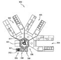
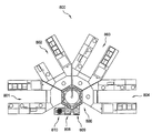
- H01L21/67167—Apparatus for manufacturing or treating in a plurality of work-stations characterized by the layout of the process chambers surrounding a central transfer chamber
-
- H—ELECTRICITY
- H01—ELECTRIC ELEMENTS
- H01L—SEMICONDUCTOR DEVICES NOT COVERED BY CLASS H10
- H01L21/00—Processes or apparatus adapted for the manufacture or treatment of semiconductor or solid state devices or of parts thereof
- H01L21/67—Apparatus specially adapted for handling semiconductor or electric solid state devices during manufacture or treatment thereof; Apparatus specially adapted for handling wafers during manufacture or treatment of semiconductor or electric solid state devices or components ; Apparatus not specifically provided for elsewhere
- H01L21/67005—Apparatus not specifically provided for elsewhere
- H01L21/67011—Apparatus for manufacture or treatment
- H01L21/67155—Apparatus for manufacturing or treating in a plurality of work-stations
- H01L21/67207—Apparatus for manufacturing or treating in a plurality of work-stations comprising a chamber adapted to a particular process
-
- H—ELECTRICITY
- H10—SEMICONDUCTOR DEVICES; ELECTRIC SOLID-STATE DEVICES NOT OTHERWISE PROVIDED FOR
- H10H—INORGANIC LIGHT-EMITTING SEMICONDUCTOR DEVICES HAVING POTENTIAL BARRIERS
- H10H20/00—Individual inorganic light-emitting semiconductor devices having potential barriers, e.g. light-emitting diodes [LED]
- H10H20/01—Manufacture or treatment
- H10H20/011—Manufacture or treatment of bodies, e.g. forming semiconductor layers
- H10H20/013—Manufacture or treatment of bodies, e.g. forming semiconductor layers having light-emitting regions comprising only Group III-V materials
- H10H20/0133—Manufacture or treatment of bodies, e.g. forming semiconductor layers having light-emitting regions comprising only Group III-V materials with a substrate not being Group III-V materials
- H10H20/01335—Manufacture or treatment of bodies, e.g. forming semiconductor layers having light-emitting regions comprising only Group III-V materials with a substrate not being Group III-V materials the light-emitting regions comprising nitride materials
Landscapes
- Engineering & Computer Science (AREA)
- Microelectronics & Electronic Packaging (AREA)
- Condensed Matter Physics & Semiconductors (AREA)
- General Physics & Mathematics (AREA)
- Manufacturing & Machinery (AREA)
- Computer Hardware Design (AREA)
- Power Engineering (AREA)
- Chemical & Material Sciences (AREA)
- Physics & Mathematics (AREA)
- Crystallography & Structural Chemistry (AREA)
- Materials Engineering (AREA)
- Metallurgy (AREA)
- Organic Chemistry (AREA)
- General Chemical & Material Sciences (AREA)
- Chemical Kinetics & Catalysis (AREA)
- Inorganic Chemistry (AREA)
- Health & Medical Sciences (AREA)
- Toxicology (AREA)
- Chemical Vapour Deposition (AREA)
- Semiconductor Lasers (AREA)
- Led Devices (AREA)
Applications Claiming Priority (8)
| Application Number | Priority Date | Filing Date | Title |
|---|---|---|---|
| US17353609P | 2009-04-28 | 2009-04-28 | |
| US61/173,536 | 2009-04-28 | ||
| US17709809P | 2009-05-11 | 2009-05-11 | |
| US61/177,098 | 2009-05-11 | ||
| US23087709P | 2009-08-03 | 2009-08-03 | |
| US61/230,877 | 2009-08-03 | ||
| US12/751,692 US8183132B2 (en) | 2009-04-10 | 2010-03-31 | Methods for fabricating group III nitride structures with a cluster tool |
| US12/751,692 | 2010-03-31 |
Publications (1)
| Publication Number | Publication Date |
|---|---|
| KR20120003495A true KR20120003495A (ko) | 2012-01-10 |
Family
ID=43050736
Family Applications (1)
| Application Number | Title | Priority Date | Filing Date |
|---|---|---|---|
| KR1020117028399A Ceased KR20120003495A (ko) | 2009-04-28 | 2010-04-27 | Led용 클러스터 툴 |
Country Status (7)
| Country | Link |
|---|---|
| US (1) | US8183132B2 (cg-RX-API-DMAC7.html) |
| EP (1) | EP2425463A2 (cg-RX-API-DMAC7.html) |
| JP (1) | JP2012525713A (cg-RX-API-DMAC7.html) |
| KR (1) | KR20120003495A (cg-RX-API-DMAC7.html) |
| CN (1) | CN102414844B (cg-RX-API-DMAC7.html) |
| TW (1) | TW201106502A (cg-RX-API-DMAC7.html) |
| WO (1) | WO2010129292A2 (cg-RX-API-DMAC7.html) |
Cited By (1)
| Publication number | Priority date | Publication date | Assignee | Title |
|---|---|---|---|---|
| KR101445673B1 (ko) * | 2013-04-30 | 2014-10-01 | 주식회사 이엔에프테크놀로지 | 반도체 결정 성장 장치 및 방법 |
Families Citing this family (39)
| Publication number | Priority date | Publication date | Assignee | Title |
|---|---|---|---|---|
| EP2215282B1 (en) | 2007-10-11 | 2016-11-30 | Valence Process Equipment, Inc. | Chemical vapor deposition reactor |
| US7976631B2 (en) | 2007-10-16 | 2011-07-12 | Applied Materials, Inc. | Multi-gas straight channel showerhead |
| US8668775B2 (en) * | 2007-10-31 | 2014-03-11 | Toshiba Techno Center Inc. | Machine CVD shower head |
| US8293013B2 (en) * | 2008-12-30 | 2012-10-23 | Intermolecular, Inc. | Dual path gas distribution device |
| US8080466B2 (en) * | 2009-08-10 | 2011-12-20 | Applied Materials, Inc. | Method for growth of nitrogen face (N-face) polarity compound nitride semiconductor device with integrated processing system |
| US9449859B2 (en) * | 2009-10-09 | 2016-09-20 | Applied Materials, Inc. | Multi-gas centrally cooled showerhead design |
| US20110244663A1 (en) * | 2010-04-01 | 2011-10-06 | Applied Materials, Inc. | Forming a compound-nitride structure that includes a nucleation layer |
| US9441295B2 (en) * | 2010-05-14 | 2016-09-13 | Solarcity Corporation | Multi-channel gas-delivery system |
| TW201213595A (en) * | 2010-09-29 | 2012-04-01 | Hon Hai Prec Ind Co Ltd | Coating device |
| KR20120070881A (ko) * | 2010-12-22 | 2012-07-02 | 삼성엘이디 주식회사 | 발광 다이오드 제조방법 |
| KR101684859B1 (ko) * | 2011-01-05 | 2016-12-09 | 삼성전자주식회사 | 발광 다이오드 제조방법 및 이에 의하여 제조된 발광 다이오드 |
| US20120315741A1 (en) * | 2011-06-13 | 2012-12-13 | Jie Su | Enhanced magnesium incorporation into gallium nitride films through high pressure or ald-type processing |
| US20130023079A1 (en) * | 2011-07-20 | 2013-01-24 | Sang Won Kang | Fabrication of light emitting diodes (leds) using a degas process |
| KR101271247B1 (ko) * | 2011-08-02 | 2013-06-07 | 주식회사 유진테크 | 에피택셜 공정을 위한 반도체 제조설비 |
| KR101271246B1 (ko) * | 2011-08-02 | 2013-06-07 | 주식회사 유진테크 | 에피택셜 공정을 위한 반도체 제조설비 |
| KR101271248B1 (ko) * | 2011-08-02 | 2013-06-07 | 주식회사 유진테크 | 에피택셜 공정을 위한 반도체 제조설비 |
| CN103132140A (zh) * | 2011-11-23 | 2013-06-05 | 甘志银 | 氢化物气相外延装置 |
| CN104737268A (zh) | 2012-01-12 | 2015-06-24 | 第一太阳能有限公司 | 在半导体器件的不同层中提供掺杂剂浓度控制的方法和系统 |
| US8676375B2 (en) * | 2012-02-27 | 2014-03-18 | Veeco Instruments Inc. | Automated cassette-to-cassette substrate handling system |
| CN102615068B (zh) * | 2012-03-26 | 2015-05-20 | 中微半导体设备(上海)有限公司 | Mocvd设备的清洁方法 |
| KR101419705B1 (ko) * | 2012-08-24 | 2014-07-15 | 주식회사 선익시스템 | 예비 챔버가 구비된 박막 증착장치 |
| US20140124788A1 (en) * | 2012-11-06 | 2014-05-08 | Intermolecular, Inc. | Chemical Vapor Deposition System |
| KR20140074516A (ko) * | 2012-12-10 | 2014-06-18 | 서울바이오시스 주식회사 | 질화갈륨계 반도체층 성장 방법 및 발광 소자 제조 방법 |
| US9312344B2 (en) | 2013-03-13 | 2016-04-12 | Taiwan Semiconductor Manufacturing Company, Ltd. | Methods for forming semiconductor materials in STI trenches |
| US9252024B2 (en) | 2013-05-17 | 2016-02-02 | Applied Materials, Inc. | Deposition chambers with UV treatment and methods of use |
| US9520466B2 (en) | 2015-03-16 | 2016-12-13 | Taiwan Semiconductor Manufacturing Company, Ltd. | Vertical gate-all-around field effect transistors and methods of forming same |
| US9972740B2 (en) | 2015-06-07 | 2018-05-15 | Tesla, Inc. | Chemical vapor deposition tool and process for fabrication of photovoltaic structures |
| US9748434B1 (en) | 2016-05-24 | 2017-08-29 | Tesla, Inc. | Systems, method and apparatus for curing conductive paste |
| US9954136B2 (en) | 2016-08-03 | 2018-04-24 | Tesla, Inc. | Cassette optimized for an inline annealing system |
| US10115856B2 (en) | 2016-10-31 | 2018-10-30 | Tesla, Inc. | System and method for curing conductive paste using induction heating |
| US10604841B2 (en) | 2016-12-14 | 2020-03-31 | Lam Research Corporation | Integrated showerhead with thermal control for delivering radical and precursor gas to a downstream chamber to enable remote plasma film deposition |
| KR102511483B1 (ko) | 2017-02-10 | 2023-03-17 | 어플라이드 머티어리얼스, 인코포레이티드 | 딥 트렌치에서의 저온 선택적 에피택시를 위한 방법 및 장치 |
| US11015247B2 (en) | 2017-12-08 | 2021-05-25 | Lam Research Corporation | Integrated showerhead with improved hole pattern for delivering radical and precursor gas to a downstream chamber to enable remote plasma film deposition |
| CN109585517A (zh) * | 2018-12-13 | 2019-04-05 | 顾琼 | 一种用于制备透明显示屏格栅的设备及其生产工艺 |
| CN111342345B (zh) * | 2018-12-18 | 2021-05-07 | 山东华光光电子股份有限公司 | 一种GaAs基量子点激光器的制备方法 |
| WO2022192460A1 (en) | 2021-03-11 | 2022-09-15 | Applied Materials, Inc. | Systems and methods for fabrication of micro-led displays |
| US12060651B2 (en) | 2021-05-11 | 2024-08-13 | Applied Materials, Inc. | Chamber architecture for epitaxial deposition and advanced epitaxial film applications |
| US12018372B2 (en) | 2021-05-11 | 2024-06-25 | Applied Materials, Inc. | Gas injector for epitaxy and CVD chamber |
| US12091749B2 (en) | 2021-05-11 | 2024-09-17 | Applied Materials, Inc. | Method for epitaxially depositing a material on a substrate by flowing a process gas across the substrate from an upper gas inlet to an upper gas outlet and flowing a purge gas from a lower gas inlet to a lower gas outlet |
Family Cites Families (83)
| Publication number | Priority date | Publication date | Assignee | Title |
|---|---|---|---|---|
| US3063867A (en) * | 1958-12-16 | 1962-11-13 | Western Electric Co | Deposition and measurement of layer thickness |
| US4851295A (en) | 1984-03-16 | 1989-07-25 | Genus, Inc. | Low resistivity tungsten silicon composite film |
| US5348911A (en) | 1987-06-30 | 1994-09-20 | Aixtron Gmbh | Material-saving process for fabricating mixed crystals |
| USD329839S (en) * | 1990-01-31 | 1992-09-29 | Hohner Automation Societe Anonyme | Incremental coder |
| WO1992022084A1 (en) | 1991-05-21 | 1992-12-10 | Advantage Production Technology, Inc. | Organic preclean for improving vapor phase wafer etch uniformity |
| US5273588A (en) | 1992-06-15 | 1993-12-28 | Materials Research Corporation | Semiconductor wafer processing CVD reactor apparatus comprising contoured electrode gas directing means |
| US5647911A (en) | 1993-12-14 | 1997-07-15 | Sony Corporation | Gas diffuser plate assembly and RF electrode |
| US5359788A (en) * | 1993-12-22 | 1994-11-01 | Gell Jr Harold A | Coffee roaster |
| US5679152A (en) | 1994-01-27 | 1997-10-21 | Advanced Technology Materials, Inc. | Method of making a single crystals Ga*N article |
| JPH09501612A (ja) | 1994-04-08 | 1997-02-18 | マーク エー. レイ, | 選択的プラズマ成長 |
| GB9411911D0 (en) | 1994-06-14 | 1994-08-03 | Swan Thomas & Co Ltd | Improvements in or relating to chemical vapour deposition |
| US5715361A (en) | 1995-04-13 | 1998-02-03 | Cvc Products, Inc. | Rapid thermal processing high-performance multizone illuminator for wafer backside heating |
| US5636320A (en) * | 1995-05-26 | 1997-06-03 | International Business Machines Corporation | Sealed chamber with heating lamps provided within transparent tubes |
| JPH0945670A (ja) * | 1995-07-29 | 1997-02-14 | Hewlett Packard Co <Hp> | Iii族−n系結晶の気相エッチング方法および再成長方法 |
| US5667592A (en) | 1996-04-16 | 1997-09-16 | Gasonics International | Process chamber sleeve with ring seals for isolating individual process modules in a common cluster |
| JPH09295890A (ja) * | 1996-04-26 | 1997-11-18 | Mitsubishi Chem Corp | 半導体製造装置および半導体製造方法 |
| US5855675A (en) | 1997-03-03 | 1999-01-05 | Genus, Inc. | Multipurpose processing chamber for chemical vapor deposition processes |
| US6286451B1 (en) * | 1997-05-29 | 2001-09-11 | Applied Materials, Inc. | Dome: shape and temperature controlled surfaces |
| US6270569B1 (en) | 1997-06-11 | 2001-08-07 | Hitachi Cable Ltd. | Method of fabricating nitride crystal, mixture, liquid phase growth method, nitride crystal, nitride crystal powders, and vapor phase growth method |
| US6464843B1 (en) * | 1998-03-31 | 2002-10-15 | Lam Research Corporation | Contamination controlling method and apparatus for a plasma processing chamber |
| US6086673A (en) | 1998-04-02 | 2000-07-11 | Massachusetts Institute Of Technology | Process for producing high-quality III-V nitride substrates |
| WO1999066565A1 (en) * | 1998-06-18 | 1999-12-23 | University Of Florida | Method and apparatus for producing group-iii nitrides |
| US6190732B1 (en) | 1998-09-03 | 2001-02-20 | Cvc Products, Inc. | Method and system for dispensing process gas for fabricating a device on a substrate |
| US6413839B1 (en) * | 1998-10-23 | 2002-07-02 | Emcore Corporation | Semiconductor device separation using a patterned laser projection |
| US6373114B1 (en) * | 1998-10-23 | 2002-04-16 | Micron Technology, Inc. | Barrier in gate stack for improved gate dielectric integrity |
| KR100304664B1 (ko) * | 1999-02-05 | 2001-09-26 | 윤종용 | GaN막 제조 방법 |
| US6309465B1 (en) | 1999-02-18 | 2001-10-30 | Aixtron Ag. | CVD reactor |
| US6200893B1 (en) * | 1999-03-11 | 2001-03-13 | Genus, Inc | Radical-assisted sequential CVD |
| US6305314B1 (en) | 1999-03-11 | 2001-10-23 | Genvs, Inc. | Apparatus and concept for minimizing parasitic chemical vapor deposition during atomic layer deposition |
| US6540838B2 (en) * | 2000-11-29 | 2003-04-01 | Genus, Inc. | Apparatus and concept for minimizing parasitic chemical vapor deposition during atomic layer deposition |
| EP1879213B1 (en) * | 1999-05-26 | 2012-03-14 | Tokyo Electron Limited | Plasma processing apparatus |
| US6206972B1 (en) | 1999-07-08 | 2001-03-27 | Genus, Inc. | Method and apparatus for providing uniform gas delivery to substrates in CVD and PECVD processes |
| US6569765B1 (en) * | 1999-08-26 | 2003-05-27 | Cbl Technologies, Inc | Hybrid deposition system and methods |
| US6489241B1 (en) * | 1999-09-17 | 2002-12-03 | Applied Materials, Inc. | Apparatus and method for surface finishing a silicon film |
| US6503330B1 (en) * | 1999-12-22 | 2003-01-07 | Genus, Inc. | Apparatus and method to achieve continuous interface and ultrathin film during atomic layer deposition |
| US6897119B1 (en) * | 1999-12-22 | 2005-05-24 | Genus, Inc. | Apparatus and method to achieve continuous interface and ultrathin film during atomic layer deposition |
| US6551399B1 (en) * | 2000-01-10 | 2003-04-22 | Genus Inc. | Fully integrated process for MIM capacitors using atomic layer deposition |
| JP4778655B2 (ja) * | 2000-02-04 | 2011-09-21 | アイクストロン、アーゲー | 1つまたは多くの被膜を基板に沈積する方法および装置 |
| US6517634B2 (en) * | 2000-02-28 | 2003-02-11 | Applied Materials, Inc. | Chemical vapor deposition chamber lid assembly |
| JP4849705B2 (ja) | 2000-03-24 | 2012-01-11 | 東京エレクトロン株式会社 | プラズマ処理装置、プラズマ生成導入部材及び誘電体 |
| US6451713B1 (en) * | 2000-04-17 | 2002-09-17 | Mattson Technology, Inc. | UV pretreatment process for ultra-thin oxynitride formation |
| US6616870B1 (en) * | 2000-08-07 | 2003-09-09 | Shipley Company, L.L.C. | Method of producing high aspect ratio domes by vapor deposition |
| DE10043601A1 (de) * | 2000-09-01 | 2002-03-14 | Aixtron Ag | Vorrichtung und Verfahren zum Abscheiden insbesondere kristalliner Schichten auf insbesondere kristallinen Substraten |
| DE10048759A1 (de) * | 2000-09-29 | 2002-04-11 | Aixtron Gmbh | Verfahren und Vorrichtung zum Abscheiden insbesondere organischer Schichten im Wege der OVPD |
| DE10056029A1 (de) * | 2000-11-11 | 2002-05-16 | Aixtron Ag | Verfahren und Vorrichtung zur Temperatursteuerung der Oberflächentemperaturen von Substraten in einem CVD-Reaktor |
| DE10057134A1 (de) * | 2000-11-17 | 2002-05-23 | Aixtron Ag | Verfahren zum Abscheiden von insbesondere kristallinen Schichten sowie Vorrichtung zur Durchführung des Verfahrens |
| US6905547B1 (en) * | 2000-12-21 | 2005-06-14 | Genus, Inc. | Method and apparatus for flexible atomic layer deposition |
| US7348042B2 (en) * | 2001-03-19 | 2008-03-25 | Novellus Systems, Inc. | Continuous method for depositing a film by modulated ion-induced atomic layer deposition (MII-ALD) |
| JP2004525518A (ja) * | 2001-03-30 | 2004-08-19 | テクノロジーズ アンド デバイス インターナショナル インコーポレイテッド | Hvpe技術を使用したサブミクロンiii属窒化物構造を成長させる方法および装置 |
| DE10118130A1 (de) * | 2001-04-11 | 2002-10-17 | Aixtron Ag | Vorrichtung oder Verfahren zum Abscheiden von insbesondere kristallinen Schichten auf insbesondere kristallinen Substraten aus der Gasphase |
| DE10124609B4 (de) * | 2001-05-17 | 2012-12-27 | Aixtron Se | Verfahren zum Abscheiden aktiver Schichten auf Substraten |
| AU2002366856A1 (en) * | 2001-12-21 | 2003-07-09 | Aixtron Ag | Method for depositing iii-v semiconductor layers on a non-iii-v substrate |
| DE10163394A1 (de) * | 2001-12-21 | 2003-07-03 | Aixtron Ag | Verfahren und Vorrichtung zum Abscheiden kristalliner Schichten und auf kristallinen Substraten |
| KR100568701B1 (ko) * | 2002-06-19 | 2006-04-07 | 니폰덴신뎅와 가부시키가이샤 | 반도체 발광 소자 |
| DE10232731A1 (de) * | 2002-07-19 | 2004-02-05 | Aixtron Ag | Be- und Entladevorrichtung für eine Beschichtungseinrichtung |
| JP4352783B2 (ja) | 2002-08-23 | 2009-10-28 | 東京エレクトロン株式会社 | ガス供給系及び処理システム |
| US7115896B2 (en) * | 2002-12-04 | 2006-10-03 | Emcore Corporation | Semiconductor structures for gallium nitride-based devices |
| US7018940B2 (en) * | 2002-12-30 | 2006-03-28 | Genus, Inc. | Method and apparatus for providing uniform gas delivery to substrates in CVD and PECVD processes |
| JP4026529B2 (ja) * | 2003-04-10 | 2007-12-26 | 東京エレクトロン株式会社 | シャワーヘッド構造及び処理装置 |
| CN101068950A (zh) * | 2003-05-30 | 2007-11-07 | 阿维扎技术公司 | 气体分配系统 |
| DE102004009130A1 (de) * | 2004-02-25 | 2005-09-15 | Aixtron Ag | Einlasssystem für einen MOCVD-Reaktor |
| US7368368B2 (en) * | 2004-08-18 | 2008-05-06 | Cree, Inc. | Multi-chamber MOCVD growth apparatus for high performance/high throughput |
| US7682940B2 (en) * | 2004-12-01 | 2010-03-23 | Applied Materials, Inc. | Use of Cl2 and/or HCl during silicon epitaxial film formation |
| DE102004058521A1 (de) * | 2004-12-04 | 2006-06-14 | Aixtron Ag | Verfahren und Vorrichtung zum Abscheiden von dicken Gallium-Nitrit-Schichten auf einem Saphirsubstrat und zugehörigen Substrathalter |
| KR100578089B1 (ko) | 2004-12-22 | 2006-05-10 | 주식회사 시스넥스 | 수소화물기상증착 반응기 |
| US20060162661A1 (en) * | 2005-01-22 | 2006-07-27 | Applied Materials, Inc. | Mixing energized and non-energized gases for silicon nitride deposition |
| TW201443990A (zh) * | 2005-03-10 | 2014-11-16 | Univ California | 用於生長平坦半極性的氮化鎵之技術 |
| US7195934B2 (en) * | 2005-07-11 | 2007-03-27 | Applied Materials, Inc. | Method and system for deposition tuning in an epitaxial film growth apparatus |
| JP4594820B2 (ja) | 2005-08-03 | 2010-12-08 | 古河機械金属株式会社 | ハイドライド気相成長装置、iii族窒化物半導体基板の製造方法 |
| JP4803578B2 (ja) | 2005-12-08 | 2011-10-26 | 東京エレクトロン株式会社 | 成膜方法 |
| GB2436398B (en) * | 2006-03-23 | 2011-08-24 | Univ Bath | Growth method using nanostructure compliant layers and HVPE for producing high quality compound semiconductor materials |
| US20070240631A1 (en) * | 2006-04-14 | 2007-10-18 | Applied Materials, Inc. | Epitaxial growth of compound nitride semiconductor structures |
| US7364991B2 (en) * | 2006-04-27 | 2008-04-29 | Applied Materials, Inc. | Buffer-layer treatment of MOCVD-grown nitride structures |
| US7459380B2 (en) * | 2006-05-05 | 2008-12-02 | Applied Materials, Inc. | Dislocation-specific dielectric mask deposition and lateral epitaxial overgrowth to reduce dislocation density of nitride films |
| US7585769B2 (en) * | 2006-05-05 | 2009-09-08 | Applied Materials, Inc. | Parasitic particle suppression in growth of III-V nitride films using MOCVD and HVPE |
| US20080050889A1 (en) * | 2006-08-24 | 2008-02-28 | Applied Materials, Inc. | Hotwall reactor and method for reducing particle formation in GaN MOCVD |
| JP2008066490A (ja) | 2006-09-06 | 2008-03-21 | Nippon Emc Ltd | 気相成長装置 |
| JP2008235758A (ja) * | 2007-03-23 | 2008-10-02 | Sumitomo Chemical Co Ltd | 化合物半導体エピタキシャル基板の製造方法 |
| KR20100075597A (ko) * | 2007-10-04 | 2010-07-02 | 어플라이드 머티어리얼스, 인코포레이티드 | 금속유기 화학기상증착 및 하이드라이드 기상 에피택시를 이용한 ⅲⅴ 질화물 필름의 성장 중에 기생형 입자의 형성을 억제하는 방법 |
| US20090149008A1 (en) * | 2007-10-05 | 2009-06-11 | Applied Materials, Inc. | Method for depositing group iii/v compounds |
| US20090194026A1 (en) | 2008-01-31 | 2009-08-06 | Burrows Brian H | Processing system for fabricating compound nitride semiconductor devices |
| US8110889B2 (en) * | 2009-04-28 | 2012-02-07 | Applied Materials, Inc. | MOCVD single chamber split process for LED manufacturing |
| US8465587B2 (en) * | 2009-12-30 | 2013-06-18 | Cbl Technologies, Inc. | Modern hydride vapor-phase epitaxy system and methods |
-
2010
- 2010-03-31 US US12/751,692 patent/US8183132B2/en active Active
- 2010-04-27 CN CN201080019514.1A patent/CN102414844B/zh active Active
- 2010-04-27 JP JP2012508596A patent/JP2012525713A/ja active Pending
- 2010-04-27 WO PCT/US2010/032597 patent/WO2010129292A2/en not_active Ceased
- 2010-04-27 EP EP10772533A patent/EP2425463A2/en not_active Withdrawn
- 2010-04-27 KR KR1020117028399A patent/KR20120003495A/ko not_active Ceased
- 2010-04-28 TW TW099113540A patent/TW201106502A/zh unknown
Cited By (1)
| Publication number | Priority date | Publication date | Assignee | Title |
|---|---|---|---|---|
| KR101445673B1 (ko) * | 2013-04-30 | 2014-10-01 | 주식회사 이엔에프테크놀로지 | 반도체 결정 성장 장치 및 방법 |
Also Published As
| Publication number | Publication date |
|---|---|
| US8183132B2 (en) | 2012-05-22 |
| TW201106502A (en) | 2011-02-16 |
| CN102414844B (zh) | 2015-04-08 |
| CN102414844A (zh) | 2012-04-11 |
| WO2010129292A2 (en) | 2010-11-11 |
| JP2012525713A (ja) | 2012-10-22 |
| US20100261340A1 (en) | 2010-10-14 |
| EP2425463A2 (en) | 2012-03-07 |
| WO2010129292A4 (en) | 2011-03-31 |
| WO2010129292A3 (en) | 2011-02-17 |
Similar Documents
| Publication | Publication Date | Title |
|---|---|---|
| US8183132B2 (en) | Methods for fabricating group III nitride structures with a cluster tool | |
| US8110889B2 (en) | MOCVD single chamber split process for LED manufacturing | |
| US8080466B2 (en) | Method for growth of nitrogen face (N-face) polarity compound nitride semiconductor device with integrated processing system | |
| US20110244617A1 (en) | Forming a compound-nitride structure that includes a nucleation layer | |
| US8642368B2 (en) | Enhancement of LED light extraction with in-situ surface roughening | |
| US20110081771A1 (en) | Multichamber split processes for led manufacturing | |
| US8138069B2 (en) | Substrate pretreatment for subsequent high temperature group III depositions | |
| US20100279020A1 (en) | METHOD OF FORMING IN-SITU PRE-GaN DEPOSITION LAYER IN HVPE | |
| US20090194026A1 (en) | Processing system for fabricating compound nitride semiconductor devices | |
| CN102484175A (zh) | 具有提高的量子效率的发光二极管和制造方法 | |
| US10439099B2 (en) | UV light emitting devices and systems and methods for production | |
| US20110207256A1 (en) | In-situ acceptor activation with nitrogen and/or oxygen plasma treatment | |
| US20110171758A1 (en) | Reclamation of scrap materials for led manufacturing | |
| US20140235007A1 (en) | Method of manufacturing semiconductor light emitting device and chemical vapor deposition apparatus | |
| WO2010129289A2 (en) | Decontamination of mocvd chamber using nh3 purge after in-situ cleaning | |
| WO2012009257A2 (en) | P-gan fabrication process utilizing a dedicated chamber and method of minimizing magnesium redistribution for sharper decay profile | |
| US8318522B2 (en) | Surface passivation techniques for chamber-split processing |
Legal Events
| Date | Code | Title | Description |
|---|---|---|---|
| PA0105 | International application |
Patent event date: 20111128 Patent event code: PA01051R01D Comment text: International Patent Application |
|
| PG1501 | Laying open of application | ||
| A201 | Request for examination | ||
| PA0201 | Request for examination |
Patent event code: PA02012R01D Patent event date: 20150423 Comment text: Request for Examination of Application |
|
| E902 | Notification of reason for refusal | ||
| PE0902 | Notice of grounds for rejection |
Comment text: Notification of reason for refusal Patent event date: 20160819 Patent event code: PE09021S01D |
|
| E902 | Notification of reason for refusal | ||
| PE0902 | Notice of grounds for rejection |
Comment text: Notification of reason for refusal Patent event date: 20170627 Patent event code: PE09021S01D |
|
| E601 | Decision to refuse application | ||
| PE0601 | Decision on rejection of patent |
Patent event date: 20171016 Comment text: Decision to Refuse Application Patent event code: PE06012S01D Patent event date: 20170627 Comment text: Notification of reason for refusal Patent event code: PE06011S01I Patent event date: 20160819 Comment text: Notification of reason for refusal Patent event code: PE06011S01I |