JP2012525713A - Led向けのクラスタツール - Google Patents
Led向けのクラスタツール Download PDFInfo
- Publication number
- JP2012525713A JP2012525713A JP2012508596A JP2012508596A JP2012525713A JP 2012525713 A JP2012525713 A JP 2012525713A JP 2012508596 A JP2012508596 A JP 2012508596A JP 2012508596 A JP2012508596 A JP 2012508596A JP 2012525713 A JP2012525713 A JP 2012525713A
- Authority
- JP
- Japan
- Prior art keywords
- processing chamber
- substrates
- chamber
- group iii
- nitride layer
- Prior art date
- Legal status (The legal status is an assumption and is not a legal conclusion. Google has not performed a legal analysis and makes no representation as to the accuracy of the status listed.)
- Pending
Links
Images


Classifications
-
- H—ELECTRICITY
- H01—ELECTRIC ELEMENTS
- H01L—SEMICONDUCTOR DEVICES NOT COVERED BY CLASS H10
- H01L21/00—Processes or apparatus adapted for the manufacture or treatment of semiconductor or solid state devices or of parts thereof
- H01L21/02—Manufacture or treatment of semiconductor devices or of parts thereof
- H01L21/02104—Forming layers
- H01L21/02365—Forming inorganic semiconducting materials on a substrate
- H01L21/02436—Intermediate layers between substrates and deposited layers
- H01L21/02439—Materials
- H01L21/02455—Group 13/15 materials
- H01L21/02458—Nitrides
-
- C—CHEMISTRY; METALLURGY
- C30—CRYSTAL GROWTH
- C30B—SINGLE-CRYSTAL GROWTH; UNIDIRECTIONAL SOLIDIFICATION OF EUTECTIC MATERIAL OR UNIDIRECTIONAL DEMIXING OF EUTECTOID MATERIAL; REFINING BY ZONE-MELTING OF MATERIAL; PRODUCTION OF A HOMOGENEOUS POLYCRYSTALLINE MATERIAL WITH DEFINED STRUCTURE; SINGLE CRYSTALS OR HOMOGENEOUS POLYCRYSTALLINE MATERIAL WITH DEFINED STRUCTURE; AFTER-TREATMENT OF SINGLE CRYSTALS OR A HOMOGENEOUS POLYCRYSTALLINE MATERIAL WITH DEFINED STRUCTURE; APPARATUS THEREFOR
- C30B25/00—Single-crystal growth by chemical reaction of reactive gases, e.g. chemical vapour-deposition growth
- C30B25/02—Epitaxial-layer growth
-
- C—CHEMISTRY; METALLURGY
- C30—CRYSTAL GROWTH
- C30B—SINGLE-CRYSTAL GROWTH; UNIDIRECTIONAL SOLIDIFICATION OF EUTECTIC MATERIAL OR UNIDIRECTIONAL DEMIXING OF EUTECTOID MATERIAL; REFINING BY ZONE-MELTING OF MATERIAL; PRODUCTION OF A HOMOGENEOUS POLYCRYSTALLINE MATERIAL WITH DEFINED STRUCTURE; SINGLE CRYSTALS OR HOMOGENEOUS POLYCRYSTALLINE MATERIAL WITH DEFINED STRUCTURE; AFTER-TREATMENT OF SINGLE CRYSTALS OR A HOMOGENEOUS POLYCRYSTALLINE MATERIAL WITH DEFINED STRUCTURE; APPARATUS THEREFOR
- C30B29/00—Single crystals or homogeneous polycrystalline material with defined structure characterised by the material or by their shape
- C30B29/10—Inorganic compounds or compositions
- C30B29/40—AIIIBV compounds wherein A is B, Al, Ga, In or Tl and B is N, P, As, Sb or Bi
- C30B29/403—AIII-nitrides
- C30B29/406—Gallium nitride
-
- H—ELECTRICITY
- H01—ELECTRIC ELEMENTS
- H01L—SEMICONDUCTOR DEVICES NOT COVERED BY CLASS H10
- H01L21/00—Processes or apparatus adapted for the manufacture or treatment of semiconductor or solid state devices or of parts thereof
- H01L21/02—Manufacture or treatment of semiconductor devices or of parts thereof
- H01L21/02104—Forming layers
- H01L21/02365—Forming inorganic semiconducting materials on a substrate
- H01L21/02367—Substrates
- H01L21/0237—Materials
- H01L21/0242—Crystalline insulating materials
-
- H—ELECTRICITY
- H01—ELECTRIC ELEMENTS
- H01L—SEMICONDUCTOR DEVICES NOT COVERED BY CLASS H10
- H01L21/00—Processes or apparatus adapted for the manufacture or treatment of semiconductor or solid state devices or of parts thereof
- H01L21/02—Manufacture or treatment of semiconductor devices or of parts thereof
- H01L21/02104—Forming layers
- H01L21/02365—Forming inorganic semiconducting materials on a substrate
- H01L21/02518—Deposited layers
- H01L21/02521—Materials
- H01L21/02538—Group 13/15 materials
- H01L21/0254—Nitrides
-
- H—ELECTRICITY
- H01—ELECTRIC ELEMENTS
- H01L—SEMICONDUCTOR DEVICES NOT COVERED BY CLASS H10
- H01L21/00—Processes or apparatus adapted for the manufacture or treatment of semiconductor or solid state devices or of parts thereof
- H01L21/02—Manufacture or treatment of semiconductor devices or of parts thereof
- H01L21/02104—Forming layers
- H01L21/02365—Forming inorganic semiconducting materials on a substrate
- H01L21/02612—Formation types
- H01L21/02617—Deposition types
- H01L21/0262—Reduction or decomposition of gaseous compounds, e.g. CVD
-
- H—ELECTRICITY
- H01—ELECTRIC ELEMENTS
- H01L—SEMICONDUCTOR DEVICES NOT COVERED BY CLASS H10
- H01L21/00—Processes or apparatus adapted for the manufacture or treatment of semiconductor or solid state devices or of parts thereof
- H01L21/67—Apparatus specially adapted for handling semiconductor or electric solid state devices during manufacture or treatment thereof; Apparatus specially adapted for handling wafers during manufacture or treatment of semiconductor or electric solid state devices or components ; Apparatus not specifically provided for elsewhere
- H01L21/67005—Apparatus not specifically provided for elsewhere
- H01L21/67011—Apparatus for manufacture or treatment
- H01L21/67098—Apparatus for thermal treatment
- H01L21/67109—Apparatus for thermal treatment mainly by convection
-
- H—ELECTRICITY
- H01—ELECTRIC ELEMENTS
- H01L—SEMICONDUCTOR DEVICES NOT COVERED BY CLASS H10
- H01L21/00—Processes or apparatus adapted for the manufacture or treatment of semiconductor or solid state devices or of parts thereof
- H01L21/67—Apparatus specially adapted for handling semiconductor or electric solid state devices during manufacture or treatment thereof; Apparatus specially adapted for handling wafers during manufacture or treatment of semiconductor or electric solid state devices or components ; Apparatus not specifically provided for elsewhere
- H01L21/67005—Apparatus not specifically provided for elsewhere
- H01L21/67011—Apparatus for manufacture or treatment
- H01L21/67098—Apparatus for thermal treatment
- H01L21/67115—Apparatus for thermal treatment mainly by radiation
-
- H—ELECTRICITY
- H01—ELECTRIC ELEMENTS
- H01L—SEMICONDUCTOR DEVICES NOT COVERED BY CLASS H10
- H01L21/00—Processes or apparatus adapted for the manufacture or treatment of semiconductor or solid state devices or of parts thereof
- H01L21/67—Apparatus specially adapted for handling semiconductor or electric solid state devices during manufacture or treatment thereof; Apparatus specially adapted for handling wafers during manufacture or treatment of semiconductor or electric solid state devices or components ; Apparatus not specifically provided for elsewhere
- H01L21/67005—Apparatus not specifically provided for elsewhere
- H01L21/67011—Apparatus for manufacture or treatment
- H01L21/67155—Apparatus for manufacturing or treating in a plurality of work-stations
- H01L21/67161—Apparatus for manufacturing or treating in a plurality of work-stations characterized by the layout of the process chambers
- H01L21/67167—Apparatus for manufacturing or treating in a plurality of work-stations characterized by the layout of the process chambers surrounding a central transfer chamber
-
- H—ELECTRICITY
- H01—ELECTRIC ELEMENTS
- H01L—SEMICONDUCTOR DEVICES NOT COVERED BY CLASS H10
- H01L21/00—Processes or apparatus adapted for the manufacture or treatment of semiconductor or solid state devices or of parts thereof
- H01L21/67—Apparatus specially adapted for handling semiconductor or electric solid state devices during manufacture or treatment thereof; Apparatus specially adapted for handling wafers during manufacture or treatment of semiconductor or electric solid state devices or components ; Apparatus not specifically provided for elsewhere
- H01L21/67005—Apparatus not specifically provided for elsewhere
- H01L21/67011—Apparatus for manufacture or treatment
- H01L21/67155—Apparatus for manufacturing or treating in a plurality of work-stations
- H01L21/67207—Apparatus for manufacturing or treating in a plurality of work-stations comprising a chamber adapted to a particular process
-
- H—ELECTRICITY
- H01—ELECTRIC ELEMENTS
- H01L—SEMICONDUCTOR DEVICES NOT COVERED BY CLASS H10
- H01L33/00—Semiconductor devices with at least one potential-jump barrier or surface barrier specially adapted for light emission; Processes or apparatus specially adapted for the manufacture or treatment thereof or of parts thereof; Details thereof
- H01L33/005—Processes
- H01L33/0062—Processes for devices with an active region comprising only III-V compounds
- H01L33/0066—Processes for devices with an active region comprising only III-V compounds with a substrate not being a III-V compound
- H01L33/007—Processes for devices with an active region comprising only III-V compounds with a substrate not being a III-V compound comprising nitride compounds
Abstract
【選択図】図4
Description
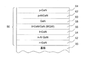
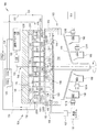
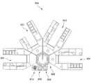
図4は、本発明の一実施形態によるクラスタツール500の平面図である。クラスタツール500は、LED向けの窒化化合物構造を形成するように構成される。

以下の実施例は、クラスタツール500に関連して説明した窒化化合物構造の製作に概略的なプロセスをどのように使用できるかを示すために提供する。この実施例はLED構造を参照し、LED構造の製作は、クラスタツール500を使用して実行される。クラスタツール500では、チャンバ502がHVPEチャンバまたはMOCVDチャンバであり、チャンバ503、504がMOCVDチャンバである。一実施形態では、LED構造は、図1Aの構造10に類似している。このプロセスの概要は、図7のフロー図で提供した。最初のIII1−N層(たとえば、GaN層)の堆積は、MOCVDプロセスまたはHVPEプロセスによってチャンバ502内で実行され、III2−N層(たとえば、InGaN層)の堆積は、第2のMOCVDチャンバ503内で実行され、III3−N層(たとえば、AlGaNおよびGaNコンタクト層)の堆積は、第3のMOCVDチャンバ504内で実行される。
Claims (24)
- 第1の処理チャンバ内に配置された2つ以上の基板上に第III族窒化物層を形成するステップと、
制御された環境内で前記2つ以上の基板を前記第1の処理チャンバから第2の処理チャンバへ移動させるステップと、
前記第2の処理チャンバ内で前記第III族窒化物層を覆って三元の第III族窒化物層を形成するステップと、
制御された環境内で前記2つ以上の基板を前記第2の処理チャンバから第3の処理チャンバへ移動させるステップと、
前記第3の処理チャンバ内で前記三元の第III族窒化物層を覆って第1のドープ第III族窒化物層を形成するステップと、
を含む、窒化化合物構造を製作する方法。 - 前記第1のドープ第III族窒化物層上に第2のドープ第III族窒化物層を形成するステップをさらに含む、請求項1に記載の方法。
- 第2のドープ第III族窒化物層が、前記第3の処理チャンバ内で前記第1のドープ第III族窒化物層を覆って形成される、請求項2に記載の方法。
- 第1の処理チャンバ内の前記2つ以上の基板上に形成される前記第III族窒化物層が、第3のドープ第III族窒化物層を含む、請求項1に記載の方法。
- 前記第III族窒化物層を形成するステップが、
HVPE前駆体を覆って塩素ガスを含む反応性ガスを流して、第1の反応生成物を形成するステップであって、前記第1の反応生成物が塩化ガリウムまたは塩化アンモニウムを含む、ステップと、
前記第1の処理チャンバ内に配置された前記2つ以上の基板の表面へ前記形成された第1の反応生成物を流すステップと、
を含む、請求項1に記載の方法。 - 第1の処理チャンバ内に配置された2つ以上の基板の表面へアンモニアおよびハロゲンガスを含むガス混合物を流しながら、前記2つ以上の基板へ熱を送達するステップと、
前記第1の処理チャンバ内に配置された前記2つ以上の基板の表面上に第III族窒化物層を形成するステップと、
制御された環境内で前記2つ以上の基板を前記第1の処理チャンバから第2の処理チャンバへ移動させるステップと、
前記第2の処理チャンバ内で前記第III族窒化物層を覆って三元の第III族窒化物層を形成するステップと、
制御された環境内で前記2つ以上の基板を前記第2の処理チャンバから第3の処理チャンバへ移動させるステップと、
前記第3の処理チャンバ内で前記三元の第III族窒化物層を覆って第1のドープ第III族窒化物層を形成するステップと、
前記第1のドープ第III族窒化物層上に第2のドープ第III族窒化物層を形成するステップと、
を含む、窒化化合物半導体構造を製作する方法。 - 前記ハロゲンガスが、フッ素ガスまたは塩素ガスを含む、請求項6に記載の方法。
- 第1の処理チャンバ内の前記2つ以上の基板上に形成される前記第III族窒化物層が、第3のドープ第III族窒化物層を含む、請求項6に記載の方法。
- 前記第III族窒化物層を形成するステップが、
HVPE前駆体を覆って塩素ガスを含む反応性ガスを流して、第1の反応生成物を形成するステップであって、前記第1の反応生成物が塩化ガリウムまたは塩化アンモニウムを含む、ステップと、
前記第1の処理チャンバ内に配置された前記2つ以上の基板の表面へ前記形成された第1の反応生成物を流すステップと、
を含む、請求項6に記載の方法。 - 水素化物気相エピタキシャル(HVPE)プロセスによって第1の処理チャンバ内で2つ以上の基板上に窒化ガリウム(GaN)層を形成するステップと、
前記2つ以上の基板を第2の処理チャンバへ移動させるステップと、
MOCVDプロセスによって前記第2の処理チャンバ内で前記2つ以上の基板上にInGaN層を形成するステップと、
前記2つ以上の基板を第3の処理チャンバへ移動させるステップと、
MOCVDプロセスによって前記第3の処理チャンバ内で前記2つ以上の基板上にpドープAlGaN層を形成するステップと、
MOCVDプロセスによって前記2つ以上の基板上にpドープGaN層を形成するステップと
を含む、窒化化合物構造を製作する方法。 - 前記InGaN層を形成するステップが、ガス分配装置を通って前記第2の処理チャンバのプロセス体積内へ2つ以上のプロセスガスを流して、前記2つ以上の基板上に1つまたは複数の膜を堆積させるステップを含む、請求項10に記載の方法。
- 前記InGaN層を形成するステップが、
複数の同心状の熱区間を形成するように構成されたランプアレイを含む熱源を使用して前記2つ以上の基板を加熱するステップをさらに含む、請求項11に記載の方法。 - 1つ以上の基板の表面へアンモニアおよびキャリアガスを含むガス混合物を流しながら、2つ以上の基板へ熱を送達するステップと、
水素化物気相エピタキシャル(HVPE)チャンバ内に配置された前記1つ以上の基板の表面へ第1のガリウム含有反応生成物および第1の窒素含有前駆体を流して、前記表面上に窒化ガリウム層を形成するステップであって、前記第1の反応生成物が
HVPE前駆体を覆って塩素を含む反応性ガスを流すことにより形成され、前記第1の反応生成物が塩化ガリウムまたは塩化アルミニウムを含む、ステップと、
前記1つ以上の基板を大気に露出させないで前記HVPEチャンバから前記1つ以上の基板を取り出すステップと、
前記1つ以上の基板を第1のMOCVDチャンバ内へ移動させるステップと、
前記第1のMOCVD処理チャンバ内へ第1のガリウム含有前駆体、インジウム含有前駆体、および第2の窒素含有前駆体を流して、前記窒化ガリウム層を覆ってInGaN層を形成するステップと、
前記1つ以上の基板を大気に露出させないで前記第1のMOCVDチャンバから前記1つ以上の基板を取り出すステップと、
前記1つ以上の基板を第2のMOCVDチャンバ内へ移動させるステップと、
前記第2のMOCVD処理チャンバ内へ第2のガリウム含有前駆体、アルミニウム含有前駆体、および第3の窒素含有前駆体を流して、前記InGaN層を覆ってAlGaN層を形成するステップと、
を含む、窒化化合物半導体構造を製作する方法。 - 前記InGaN層を形成するステップが、ガス分配装置を通って前記第2の処理チャンバのプロセス体積内へ2つ以上のプロセスガスを流して、前記2つ以上の基板上に1つまたは複数の膜を堆積させるステップを含む、請求項13に記載の方法。
- 前記InGaN層を形成するステップが、
複数の同心状の熱区間を形成するように構成されたランプアレイを含む熱源を使用して前記2つ以上の基板を加熱するステップをさらに含む、請求項14に記載の方法。 - 第1の処理チャンバ内に配置された2つ以上の基板上に第III族窒化物層を形成するステップと、
制御された環境内で前記2つ以上の基板を前記第1の処理チャンバから第2の処理チャンバへ移動させるステップと、
前記第2の処理チャンバ内で前記第III族窒化物層を覆って三元の第III族窒化物層を形成するステップと、
制御された環境内で前記2つ以上の基板を前記第2の処理チャンバから第3の処理チャンバへ移動させるステップと、
前記第3の処理チャンバ内で前記三元の第III族窒化物層を覆って第1のドープ第III族窒化物層を形成するステップと、
制御された環境内で前記2つ以上の基板を前記第3の処理チャンバから第4の処理チャンバへ移動させるステップと、
前記第4の処理チャンバ内で前記第1のドープ第III族窒化物層上に第2のドープ第III族窒化物層を形成するステップと、
を含む、窒化化合物構造を製作する方法。 - 第1の処理チャンバ内の前記2つ以上の基板上に形成される前記第III族窒化物層が、第3のドープ第III族窒化物層を含む、請求項16に記載の方法。
- 前記2つ以上の基板上に前記第III族窒化物層を形成する前に、前記2つ以上の基板へ熱を送達し、かつ、前記2つ以上の基板の表面へアンモニアおよびハロゲンガスを含むガス混合物を流すステップをさらに含む、請求項16に記載の方法。
- 前記第III族窒化物層を形成するステップが、
HVPE前駆体を覆って塩素ガスを含む反応性ガスを流して、第1の反応生成物を形成するステップであって、前記第1の反応生成物が塩化ガリウムまたは塩化アンモニウムを含む、ステップと、
前記第1の処理チャンバ内に配置された前記2つ以上の基板の表面へ前記形成された第1の反応生成物を流すステップと、
を含む、請求項16に記載の方法。 - 第1の処理チャンバ内に配置された2つ以上の基板上に三元の第III族窒化物層を形成するステップと、
制御された環境内で前記2つ以上の基板を前記第1の処理チャンバから第2の処理チャンバへ移動させるステップと、
前記第2の処理チャンバ内で前記三元の第III族窒化物層を覆って第1のドープ第III族窒化物層を形成するステップと、
前記第1のドープ第III族窒化物層上に第2のドープ第III族窒化物層を形成するステップと、
を含む、窒化化合物構造を製作する方法。 - 第2のドープ第III族窒化物層が、前記第3の処理チャンバ内で前記第1のドープ第III族窒化物層を覆って形成される、請求項20に記載の方法。
- 2つ以上の基板へ熱を送達し、かつ、第1の処理チャンバ内に配置された前記2つ以上の基板の表面へアンモニアおよびハロゲンガスを含むガス混合物を流すステップと、
前記第1の処理チャンバ内で前記2つ以上の基板の各々の表面上に窒化ガリウム層を形成するステップと、
制御された環境内で前記2つ以上の基板を前記第1の処理チャンバから第2の処理チャンバへ移動させるステップと、
前記第2の処理チャンバ内で前記窒化ガリウム層を覆って第1のドープ第III族窒化物層を形成するステップと、
を含む、窒化化合物構造を製作する方法。 - 前記第1のドープ第III族窒化物層が、窒化ガリウムを含む、請求項22に記載の方法。
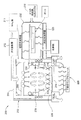
- 移動領域を画定する密閉容器と、
前記移動領域と移動可能に連通しているHVPE処理チャンバであって、前記HVPE処理チャンバが、
処理中、前記HVPE処理チャンバの処理体積内に配置されたキャリア板を加熱するように位置した加熱源であって、前記キャリア板が1つまたは複数の基板を受け取るように構成されている、加熱源、
液体ガリウムを保持するように構成されている領域を有する供給源ボート、および、
前記供給源ボートの前記領域に結合されている塩素ガス源、を含む、HVPE処理チャンバと、
前記移動領域と移動可能に連通しており、かつ、前記1つまたは複数の基板上に1つまたは複数の窒化化合物半導体層を形成するように動作可能な第1のMOCVD処理チャンバであって、前記第1の処理チャンバが、
前記処理チャンバの処理体積内に位置した基板支持体、
前記処理領域の頂部を画定するシャワーヘッド、
前記シャワーヘッドを通って前記処理領域と結合している有機金属インジウム含有供給源および有機金属ガリウム含有供給源、ならびに、
前記処理領域の下に位置し、かつ、前記基板支持体の方へ放射熱を誘導するように位置された1つまたは複数の加熱区間を形成する複数の加熱源、を含む、第1のMOCVD処理チャンバと、
前記移動領域と移動可能に連通しており、かつ、前記1つまたは複数の基板上に1つまたは複数の窒化化合物半導体層を形成するように動作可能な第2のMOCVD処理チャンバであって、前記第2の処理チャンバが、
前記処理チャンバの処理体積内に位置した基板支持体、
前記処理領域の頂部を画定するシャワーヘッド、
前記シャワーヘッドを通って前記処理領域と結合している有機金属アルミニウム含有供給源、Cp2Mg含有供給源および有機金属ガリウム含有供給源、ならびに、
前記処理領域の下に位置し、かつ、前記基板支持体の方へ放射熱を誘導するように位置された1つまたは複数の加熱区間を形成する複数の加熱源、を含む、第2のMOCVD処理チャンバと、
前記移動領域と移動可能に連通している空胴を画定するロードロックチャンバであって、前記空胴が複数のキャリア板を受け取るように構成されており、かつ、前記空胴内に配置された前記基板へ清浄ガスを送達するように適合された清浄ガス源と流体連通している、ロードロックチャンバと、
を含む、窒化化合物半導体構造を製作するシステム。
Applications Claiming Priority (9)
| Application Number | Priority Date | Filing Date | Title |
|---|---|---|---|
| US17353609P | 2009-04-28 | 2009-04-28 | |
| US61/173,536 | 2009-04-28 | ||
| US17709809P | 2009-05-11 | 2009-05-11 | |
| US61/177,098 | 2009-05-11 | ||
| US23087709P | 2009-08-03 | 2009-08-03 | |
| US61/230,877 | 2009-08-03 | ||
| US12/751,692 | 2010-03-31 | ||
| US12/751,692 US8183132B2 (en) | 2009-04-10 | 2010-03-31 | Methods for fabricating group III nitride structures with a cluster tool |
| PCT/US2010/032597 WO2010129292A2 (en) | 2009-04-28 | 2010-04-27 | Cluster tool for leds |
Publications (2)
| Publication Number | Publication Date |
|---|---|
| JP2012525713A true JP2012525713A (ja) | 2012-10-22 |
| JP2012525713A5 JP2012525713A5 (ja) | 2013-06-20 |
Family
ID=43050736
Family Applications (1)
| Application Number | Title | Priority Date | Filing Date |
|---|---|---|---|
| JP2012508596A Pending JP2012525713A (ja) | 2009-04-28 | 2010-04-27 | Led向けのクラスタツール |
Country Status (7)
| Country | Link |
|---|---|
| US (1) | US8183132B2 (ja) |
| EP (1) | EP2425463A2 (ja) |
| JP (1) | JP2012525713A (ja) |
| KR (1) | KR20120003495A (ja) |
| CN (1) | CN102414844B (ja) |
| TW (1) | TW201106502A (ja) |
| WO (1) | WO2010129292A2 (ja) |
Families Citing this family (34)
| Publication number | Priority date | Publication date | Assignee | Title |
|---|---|---|---|---|
| JP2011500961A (ja) | 2007-10-11 | 2011-01-06 | バレンス プロセス イクウィップメント,インコーポレイテッド | 化学気相成長反応器 |
| US7976631B2 (en) * | 2007-10-16 | 2011-07-12 | Applied Materials, Inc. | Multi-gas straight channel showerhead |
| US8668775B2 (en) * | 2007-10-31 | 2014-03-11 | Toshiba Techno Center Inc. | Machine CVD shower head |
| US8293013B2 (en) * | 2008-12-30 | 2012-10-23 | Intermolecular, Inc. | Dual path gas distribution device |
| US8080466B2 (en) * | 2009-08-10 | 2011-12-20 | Applied Materials, Inc. | Method for growth of nitrogen face (N-face) polarity compound nitride semiconductor device with integrated processing system |
| US9449859B2 (en) * | 2009-10-09 | 2016-09-20 | Applied Materials, Inc. | Multi-gas centrally cooled showerhead design |
| US20110244663A1 (en) * | 2010-04-01 | 2011-10-06 | Applied Materials, Inc. | Forming a compound-nitride structure that includes a nucleation layer |
| US9441295B2 (en) * | 2010-05-14 | 2016-09-13 | Solarcity Corporation | Multi-channel gas-delivery system |
| TW201213595A (en) * | 2010-09-29 | 2012-04-01 | Hon Hai Prec Ind Co Ltd | Coating device |
| KR20120070881A (ko) * | 2010-12-22 | 2012-07-02 | 삼성엘이디 주식회사 | 발광 다이오드 제조방법 |
| KR101684859B1 (ko) * | 2011-01-05 | 2016-12-09 | 삼성전자주식회사 | 발광 다이오드 제조방법 및 이에 의하여 제조된 발광 다이오드 |
| US20120315741A1 (en) * | 2011-06-13 | 2012-12-13 | Jie Su | Enhanced magnesium incorporation into gallium nitride films through high pressure or ald-type processing |
| US20130023079A1 (en) * | 2011-07-20 | 2013-01-24 | Sang Won Kang | Fabrication of light emitting diodes (leds) using a degas process |
| KR101271248B1 (ko) * | 2011-08-02 | 2013-06-07 | 주식회사 유진테크 | 에피택셜 공정을 위한 반도체 제조설비 |
| KR101271246B1 (ko) * | 2011-08-02 | 2013-06-07 | 주식회사 유진테크 | 에피택셜 공정을 위한 반도체 제조설비 |
| KR101271247B1 (ko) * | 2011-08-02 | 2013-06-07 | 주식회사 유진테크 | 에피택셜 공정을 위한 반도체 제조설비 |
| CN103132140A (zh) * | 2011-11-23 | 2013-06-05 | 甘志银 | 氢化物气相外延装置 |
| CN104737268A (zh) | 2012-01-12 | 2015-06-24 | 第一太阳能有限公司 | 在半导体器件的不同层中提供掺杂剂浓度控制的方法和系统 |
| US8676375B2 (en) * | 2012-02-27 | 2014-03-18 | Veeco Instruments Inc. | Automated cassette-to-cassette substrate handling system |
| CN102615068B (zh) * | 2012-03-26 | 2015-05-20 | 中微半导体设备(上海)有限公司 | Mocvd设备的清洁方法 |
| KR101419705B1 (ko) * | 2012-08-24 | 2014-07-15 | 주식회사 선익시스템 | 예비 챔버가 구비된 박막 증착장치 |
| US20140124788A1 (en) * | 2012-11-06 | 2014-05-08 | Intermolecular, Inc. | Chemical Vapor Deposition System |
| KR20140074516A (ko) * | 2012-12-10 | 2014-06-18 | 서울바이오시스 주식회사 | 질화갈륨계 반도체층 성장 방법 및 발광 소자 제조 방법 |
| US9312344B2 (en) | 2013-03-13 | 2016-04-12 | Taiwan Semiconductor Manufacturing Company, Ltd. | Methods for forming semiconductor materials in STI trenches |
| KR101445673B1 (ko) * | 2013-04-30 | 2014-10-01 | 주식회사 이엔에프테크놀로지 | 반도체 결정 성장 장치 및 방법 |
| US9252024B2 (en) | 2013-05-17 | 2016-02-02 | Applied Materials, Inc. | Deposition chambers with UV treatment and methods of use |
| US9520466B2 (en) | 2015-03-16 | 2016-12-13 | Taiwan Semiconductor Manufacturing Company, Ltd. | Vertical gate-all-around field effect transistors and methods of forming same |
| US20160359080A1 (en) | 2015-06-07 | 2016-12-08 | Solarcity Corporation | System, method and apparatus for chemical vapor deposition |
| US9748434B1 (en) | 2016-05-24 | 2017-08-29 | Tesla, Inc. | Systems, method and apparatus for curing conductive paste |
| US9954136B2 (en) | 2016-08-03 | 2018-04-24 | Tesla, Inc. | Cassette optimized for an inline annealing system |
| US10115856B2 (en) | 2016-10-31 | 2018-10-30 | Tesla, Inc. | System and method for curing conductive paste using induction heating |
| US10604841B2 (en) * | 2016-12-14 | 2020-03-31 | Lam Research Corporation | Integrated showerhead with thermal control for delivering radical and precursor gas to a downstream chamber to enable remote plasma film deposition |
| CN109585517A (zh) * | 2018-12-13 | 2019-04-05 | 顾琼 | 一种用于制备透明显示屏格栅的设备及其生产工艺 |
| CN111342345B (zh) * | 2018-12-18 | 2021-05-07 | 山东华光光电子股份有限公司 | 一种GaAs基量子点激光器的制备方法 |
Citations (5)
| Publication number | Priority date | Publication date | Assignee | Title |
|---|---|---|---|---|
| JPH09295890A (ja) * | 1996-04-26 | 1997-11-18 | Mitsubishi Chem Corp | 半導体製造装置および半導体製造方法 |
| WO2007107757A2 (en) * | 2006-03-23 | 2007-09-27 | Nanogan Limited | Growth method using nanostructure compliant layers and hvpe for producing high quality compound semiconductor materials |
| WO2007121270A1 (en) * | 2006-04-14 | 2007-10-25 | Applied Materials, Inc. | Epitaxial growth of iii-nitride compound semiconductors structures |
| JP2008235758A (ja) * | 2007-03-23 | 2008-10-02 | Sumitomo Chemical Co Ltd | 化合物半導体エピタキシャル基板の製造方法 |
| WO2009045217A1 (en) * | 2007-10-04 | 2009-04-09 | Applied Materials, Inc. | Parasitic particle suppression in the growth of iii-v nitride films using mocvd and hvpe |
Family Cites Families (78)
| Publication number | Priority date | Publication date | Assignee | Title |
|---|---|---|---|---|
| US3063867A (en) * | 1958-12-16 | 1962-11-13 | Western Electric Co | Deposition and measurement of layer thickness |
| US4851295A (en) | 1984-03-16 | 1989-07-25 | Genus, Inc. | Low resistivity tungsten silicon composite film |
| US5348911A (en) | 1987-06-30 | 1994-09-20 | Aixtron Gmbh | Material-saving process for fabricating mixed crystals |
| USD329839S (en) * | 1990-01-31 | 1992-09-29 | Hohner Automation Societe Anonyme | Incremental coder |
| WO1992022084A1 (en) | 1991-05-21 | 1992-12-10 | Advantage Production Technology, Inc. | Organic preclean for improving vapor phase wafer etch uniformity |
| US5273588A (en) | 1992-06-15 | 1993-12-28 | Materials Research Corporation | Semiconductor wafer processing CVD reactor apparatus comprising contoured electrode gas directing means |
| US5647911A (en) | 1993-12-14 | 1997-07-15 | Sony Corporation | Gas diffuser plate assembly and RF electrode |
| US5359788A (en) * | 1993-12-22 | 1994-11-01 | Gell Jr Harold A | Coffee roaster |
| US5679152A (en) | 1994-01-27 | 1997-10-21 | Advanced Technology Materials, Inc. | Method of making a single crystals Ga*N article |
| WO1995027570A1 (en) | 1994-04-08 | 1995-10-19 | Ray Mark A | Selective plasma deposition |
| GB9411911D0 (en) | 1994-06-14 | 1994-08-03 | Swan Thomas & Co Ltd | Improvements in or relating to chemical vapour deposition |
| US5715361A (en) | 1995-04-13 | 1998-02-03 | Cvc Products, Inc. | Rapid thermal processing high-performance multizone illuminator for wafer backside heating |
| US5636320A (en) * | 1995-05-26 | 1997-06-03 | International Business Machines Corporation | Sealed chamber with heating lamps provided within transparent tubes |
| JPH0945670A (ja) * | 1995-07-29 | 1997-02-14 | Hewlett Packard Co <Hp> | Iii族−n系結晶の気相エッチング方法および再成長方法 |
| US5667592A (en) | 1996-04-16 | 1997-09-16 | Gasonics International | Process chamber sleeve with ring seals for isolating individual process modules in a common cluster |
| US5855675A (en) | 1997-03-03 | 1999-01-05 | Genus, Inc. | Multipurpose processing chamber for chemical vapor deposition processes |
| US6286451B1 (en) * | 1997-05-29 | 2001-09-11 | Applied Materials, Inc. | Dome: shape and temperature controlled surfaces |
| US6270569B1 (en) | 1997-06-11 | 2001-08-07 | Hitachi Cable Ltd. | Method of fabricating nitride crystal, mixture, liquid phase growth method, nitride crystal, nitride crystal powders, and vapor phase growth method |
| US6464843B1 (en) * | 1998-03-31 | 2002-10-15 | Lam Research Corporation | Contamination controlling method and apparatus for a plasma processing chamber |
| US6086673A (en) | 1998-04-02 | 2000-07-11 | Massachusetts Institute Of Technology | Process for producing high-quality III-V nitride substrates |
| US6218280B1 (en) * | 1998-06-18 | 2001-04-17 | University Of Florida | Method and apparatus for producing group-III nitrides |
| US6190732B1 (en) * | 1998-09-03 | 2001-02-20 | Cvc Products, Inc. | Method and system for dispensing process gas for fabricating a device on a substrate |
| US6373114B1 (en) * | 1998-10-23 | 2002-04-16 | Micron Technology, Inc. | Barrier in gate stack for improved gate dielectric integrity |
| US6413839B1 (en) * | 1998-10-23 | 2002-07-02 | Emcore Corporation | Semiconductor device separation using a patterned laser projection |
| KR100304664B1 (ko) * | 1999-02-05 | 2001-09-26 | 윤종용 | GaN막 제조 방법 |
| US6309465B1 (en) | 1999-02-18 | 2001-10-30 | Aixtron Ag. | CVD reactor |
| US6200893B1 (en) * | 1999-03-11 | 2001-03-13 | Genus, Inc | Radical-assisted sequential CVD |
| US6540838B2 (en) * | 2000-11-29 | 2003-04-01 | Genus, Inc. | Apparatus and concept for minimizing parasitic chemical vapor deposition during atomic layer deposition |
| US6305314B1 (en) * | 1999-03-11 | 2001-10-23 | Genvs, Inc. | Apparatus and concept for minimizing parasitic chemical vapor deposition during atomic layer deposition |
| TW477009B (en) * | 1999-05-26 | 2002-02-21 | Tadahiro Ohmi | Plasma process device |
| US6206972B1 (en) * | 1999-07-08 | 2001-03-27 | Genus, Inc. | Method and apparatus for providing uniform gas delivery to substrates in CVD and PECVD processes |
| US6569765B1 (en) * | 1999-08-26 | 2003-05-27 | Cbl Technologies, Inc | Hybrid deposition system and methods |
| US6489241B1 (en) * | 1999-09-17 | 2002-12-03 | Applied Materials, Inc. | Apparatus and method for surface finishing a silicon film |
| US6503330B1 (en) * | 1999-12-22 | 2003-01-07 | Genus, Inc. | Apparatus and method to achieve continuous interface and ultrathin film during atomic layer deposition |
| US6897119B1 (en) * | 1999-12-22 | 2005-05-24 | Genus, Inc. | Apparatus and method to achieve continuous interface and ultrathin film during atomic layer deposition |
| US6551399B1 (en) * | 2000-01-10 | 2003-04-22 | Genus Inc. | Fully integrated process for MIM capacitors using atomic layer deposition |
| KR100780143B1 (ko) * | 2000-02-04 | 2007-11-27 | 아익스트론 아게 | 기재상에 하나 이상의 층을 증착하기 위한 장치와 방법 |
| US6517634B2 (en) * | 2000-02-28 | 2003-02-11 | Applied Materials, Inc. | Chemical vapor deposition chamber lid assembly |
| JP4849705B2 (ja) | 2000-03-24 | 2012-01-11 | 東京エレクトロン株式会社 | プラズマ処理装置、プラズマ生成導入部材及び誘電体 |
| JP4813737B2 (ja) | 2000-04-17 | 2011-11-09 | マットソン テクノロジー インコーポレイテッド | 窒化ケイ素フィルムを形成するための超薄オキシニトリドのuv前処理法 |
| US6616870B1 (en) * | 2000-08-07 | 2003-09-09 | Shipley Company, L.L.C. | Method of producing high aspect ratio domes by vapor deposition |
| DE10043601A1 (de) * | 2000-09-01 | 2002-03-14 | Aixtron Ag | Vorrichtung und Verfahren zum Abscheiden insbesondere kristalliner Schichten auf insbesondere kristallinen Substraten |
| DE10048759A1 (de) * | 2000-09-29 | 2002-04-11 | Aixtron Gmbh | Verfahren und Vorrichtung zum Abscheiden insbesondere organischer Schichten im Wege der OVPD |
| DE10056029A1 (de) * | 2000-11-11 | 2002-05-16 | Aixtron Ag | Verfahren und Vorrichtung zur Temperatursteuerung der Oberflächentemperaturen von Substraten in einem CVD-Reaktor |
| DE10057134A1 (de) * | 2000-11-17 | 2002-05-23 | Aixtron Ag | Verfahren zum Abscheiden von insbesondere kristallinen Schichten sowie Vorrichtung zur Durchführung des Verfahrens |
| US6905547B1 (en) * | 2000-12-21 | 2005-06-14 | Genus, Inc. | Method and apparatus for flexible atomic layer deposition |
| US7348042B2 (en) * | 2001-03-19 | 2008-03-25 | Novellus Systems, Inc. | Continuous method for depositing a film by modulated ion-induced atomic layer deposition (MII-ALD) |
| WO2002080225A2 (en) * | 2001-03-30 | 2002-10-10 | Technologies And Devices International Inc. | Method and apparatus for growing submicron group iii nitride structures utilizing hvpe techniques |
| DE10118130A1 (de) * | 2001-04-11 | 2002-10-17 | Aixtron Ag | Vorrichtung oder Verfahren zum Abscheiden von insbesondere kristallinen Schichten auf insbesondere kristallinen Substraten aus der Gasphase |
| DE10124609B4 (de) * | 2001-05-17 | 2012-12-27 | Aixtron Se | Verfahren zum Abscheiden aktiver Schichten auf Substraten |
| DE10163394A1 (de) * | 2001-12-21 | 2003-07-03 | Aixtron Ag | Verfahren und Vorrichtung zum Abscheiden kristalliner Schichten und auf kristallinen Substraten |
| AU2002366856A1 (en) * | 2001-12-21 | 2003-07-09 | Aixtron Ag | Method for depositing iii-v semiconductor layers on a non-iii-v substrate |
| KR100568701B1 (ko) * | 2002-06-19 | 2006-04-07 | 니폰덴신뎅와 가부시키가이샤 | 반도체 발광 소자 |
| DE10232731A1 (de) * | 2002-07-19 | 2004-02-05 | Aixtron Ag | Be- und Entladevorrichtung für eine Beschichtungseinrichtung |
| JP4352783B2 (ja) | 2002-08-23 | 2009-10-28 | 東京エレクトロン株式会社 | ガス供給系及び処理システム |
| US7115896B2 (en) * | 2002-12-04 | 2006-10-03 | Emcore Corporation | Semiconductor structures for gallium nitride-based devices |
| US7018940B2 (en) * | 2002-12-30 | 2006-03-28 | Genus, Inc. | Method and apparatus for providing uniform gas delivery to substrates in CVD and PECVD processes |
| JP4026529B2 (ja) * | 2003-04-10 | 2007-12-26 | 東京エレクトロン株式会社 | シャワーヘッド構造及び処理装置 |
| US6921437B1 (en) * | 2003-05-30 | 2005-07-26 | Aviza Technology, Inc. | Gas distribution system |
| DE102004009130A1 (de) * | 2004-02-25 | 2005-09-15 | Aixtron Ag | Einlasssystem für einen MOCVD-Reaktor |
| US7368368B2 (en) * | 2004-08-18 | 2008-05-06 | Cree, Inc. | Multi-chamber MOCVD growth apparatus for high performance/high throughput |
| US7682940B2 (en) * | 2004-12-01 | 2010-03-23 | Applied Materials, Inc. | Use of Cl2 and/or HCl during silicon epitaxial film formation |
| DE102004058521A1 (de) * | 2004-12-04 | 2006-06-14 | Aixtron Ag | Verfahren und Vorrichtung zum Abscheiden von dicken Gallium-Nitrit-Schichten auf einem Saphirsubstrat und zugehörigen Substrathalter |
| KR100578089B1 (ko) | 2004-12-22 | 2006-05-10 | 주식회사 시스넥스 | 수소화물기상증착 반응기 |
| US20060162661A1 (en) * | 2005-01-22 | 2006-07-27 | Applied Materials, Inc. | Mixing energized and non-energized gases for silicon nitride deposition |
| JP5706601B2 (ja) * | 2005-03-10 | 2015-04-22 | ザ リージェンツ オブ ザ ユニバーシティ オブ カリフォルニア | 平坦な半極性窒化ガリウムの成長技術 |
| US7195934B2 (en) * | 2005-07-11 | 2007-03-27 | Applied Materials, Inc. | Method and system for deposition tuning in an epitaxial film growth apparatus |
| JP4594820B2 (ja) | 2005-08-03 | 2010-12-08 | 古河機械金属株式会社 | ハイドライド気相成長装置、iii族窒化物半導体基板の製造方法 |
| JP4803578B2 (ja) | 2005-12-08 | 2011-10-26 | 東京エレクトロン株式会社 | 成膜方法 |
| US7364991B2 (en) * | 2006-04-27 | 2008-04-29 | Applied Materials, Inc. | Buffer-layer treatment of MOCVD-grown nitride structures |
| US7459380B2 (en) * | 2006-05-05 | 2008-12-02 | Applied Materials, Inc. | Dislocation-specific dielectric mask deposition and lateral epitaxial overgrowth to reduce dislocation density of nitride films |
| US7585769B2 (en) * | 2006-05-05 | 2009-09-08 | Applied Materials, Inc. | Parasitic particle suppression in growth of III-V nitride films using MOCVD and HVPE |
| US20080050889A1 (en) * | 2006-08-24 | 2008-02-28 | Applied Materials, Inc. | Hotwall reactor and method for reducing particle formation in GaN MOCVD |
| JP2008066490A (ja) | 2006-09-06 | 2008-03-21 | Nippon Emc Ltd | 気相成長装置 |
| US20090149008A1 (en) * | 2007-10-05 | 2009-06-11 | Applied Materials, Inc. | Method for depositing group iii/v compounds |
| US20090194026A1 (en) | 2008-01-31 | 2009-08-06 | Burrows Brian H | Processing system for fabricating compound nitride semiconductor devices |
| US20100273291A1 (en) * | 2009-04-28 | 2010-10-28 | Applied Materials, Inc. | Decontamination of mocvd chamber using nh3 purge after in-situ cleaning |
| US8465587B2 (en) * | 2009-12-30 | 2013-06-18 | Cbl Technologies, Inc. | Modern hydride vapor-phase epitaxy system and methods |
-
2010
- 2010-03-31 US US12/751,692 patent/US8183132B2/en active Active
- 2010-04-27 CN CN201080019514.1A patent/CN102414844B/zh active Active
- 2010-04-27 WO PCT/US2010/032597 patent/WO2010129292A2/en active Application Filing
- 2010-04-27 JP JP2012508596A patent/JP2012525713A/ja active Pending
- 2010-04-27 EP EP10772533A patent/EP2425463A2/en not_active Withdrawn
- 2010-04-27 KR KR1020117028399A patent/KR20120003495A/ko not_active Application Discontinuation
- 2010-04-28 TW TW099113540A patent/TW201106502A/zh unknown
Patent Citations (8)
| Publication number | Priority date | Publication date | Assignee | Title |
|---|---|---|---|---|
| JPH09295890A (ja) * | 1996-04-26 | 1997-11-18 | Mitsubishi Chem Corp | 半導体製造装置および半導体製造方法 |
| WO2007107757A2 (en) * | 2006-03-23 | 2007-09-27 | Nanogan Limited | Growth method using nanostructure compliant layers and hvpe for producing high quality compound semiconductor materials |
| JP2009522822A (ja) * | 2006-03-23 | 2009-06-11 | ナノガン リミテッド | 高品質化合物半導体材料を製造するためのナノ構造適応層及びhvpeを使用する成長法、単結晶化合物半導体材料、並びに、基板材料 |
| WO2007121270A1 (en) * | 2006-04-14 | 2007-10-25 | Applied Materials, Inc. | Epitaxial growth of iii-nitride compound semiconductors structures |
| JP2009533879A (ja) * | 2006-04-14 | 2009-09-17 | アプライド マテリアルズ インコーポレイテッド | 窒化化合物半導体構造のエピタキシャル成長 |
| JP2008235758A (ja) * | 2007-03-23 | 2008-10-02 | Sumitomo Chemical Co Ltd | 化合物半導体エピタキシャル基板の製造方法 |
| WO2009045217A1 (en) * | 2007-10-04 | 2009-04-09 | Applied Materials, Inc. | Parasitic particle suppression in the growth of iii-v nitride films using mocvd and hvpe |
| JP2010541276A (ja) * | 2007-10-04 | 2010-12-24 | アプライド マテリアルズ インコーポレイテッド | Mocvdとhvpeを用いたiii−v族窒化膜の成長における寄生粒子抑制 |
Also Published As
| Publication number | Publication date |
|---|---|
| CN102414844A (zh) | 2012-04-11 |
| WO2010129292A2 (en) | 2010-11-11 |
| CN102414844B (zh) | 2015-04-08 |
| US20100261340A1 (en) | 2010-10-14 |
| US8183132B2 (en) | 2012-05-22 |
| TW201106502A (en) | 2011-02-16 |
| KR20120003495A (ko) | 2012-01-10 |
| EP2425463A2 (en) | 2012-03-07 |
| WO2010129292A4 (en) | 2011-03-31 |
| WO2010129292A3 (en) | 2011-02-17 |
Similar Documents
| Publication | Publication Date | Title |
|---|---|---|
| US8183132B2 (en) | Methods for fabricating group III nitride structures with a cluster tool | |
| US8110889B2 (en) | MOCVD single chamber split process for LED manufacturing | |
| US8080466B2 (en) | Method for growth of nitrogen face (N-face) polarity compound nitride semiconductor device with integrated processing system | |
| US8778783B2 (en) | Methods for improved growth of group III nitride buffer layers | |
| US20110244617A1 (en) | Forming a compound-nitride structure that includes a nucleation layer | |
| US8138069B2 (en) | Substrate pretreatment for subsequent high temperature group III depositions | |
| US20110081771A1 (en) | Multichamber split processes for led manufacturing | |
| US8980002B2 (en) | Methods for improved growth of group III nitride semiconductor compounds | |
| US20100279020A1 (en) | METHOD OF FORMING IN-SITU PRE-GaN DEPOSITION LAYER IN HVPE | |
| TWI496935B (zh) | Mocvd腔室在原位清潔後利用nh3淨化之去汙染 | |
| JP2010510166A (ja) | 三塩化ガリウムの噴射方式 | |
| US10439099B2 (en) | UV light emitting devices and systems and methods for production | |
| US20110207256A1 (en) | In-situ acceptor activation with nitrogen and/or oxygen plasma treatment | |
| US20110171758A1 (en) | Reclamation of scrap materials for led manufacturing | |
| US20120258581A1 (en) | Mocvd fabrication of group iii-nitride materials using in-situ generated hydrazine or fragments there from | |
| US20120015502A1 (en) | p-GaN Fabrication Process Utilizing a Dedicated Chamber and Method of Minimizing Magnesium Redistribution for Sharper Decay Profile | |
| WO2010129289A2 (en) | Decontamination of mocvd chamber using nh3 purge after in-situ cleaning |
Legal Events
| Date | Code | Title | Description |
|---|---|---|---|
| A521 | Written amendment |
Free format text: JAPANESE INTERMEDIATE CODE: A523 Effective date: 20130426 |
|
| A621 | Written request for application examination |
Free format text: JAPANESE INTERMEDIATE CODE: A621 Effective date: 20130426 |
|
| A131 | Notification of reasons for refusal |
Free format text: JAPANESE INTERMEDIATE CODE: A131 Effective date: 20140708 |
|
| A601 | Written request for extension of time |
Free format text: JAPANESE INTERMEDIATE CODE: A601 Effective date: 20141003 |
|
| A602 | Written permission of extension of time |
Free format text: JAPANESE INTERMEDIATE CODE: A602 Effective date: 20141010 |
|
| A601 | Written request for extension of time |
Free format text: JAPANESE INTERMEDIATE CODE: A601 Effective date: 20141106 |
|
| A602 | Written permission of extension of time |
Free format text: JAPANESE INTERMEDIATE CODE: A602 Effective date: 20141113 |
|
| A601 | Written request for extension of time |
Free format text: JAPANESE INTERMEDIATE CODE: A601 Effective date: 20141203 |
|
| A602 | Written permission of extension of time |
Free format text: JAPANESE INTERMEDIATE CODE: A602 Effective date: 20141210 |
|
| A521 | Written amendment |
Free format text: JAPANESE INTERMEDIATE CODE: A523 Effective date: 20150108 |
|
| A02 | Decision of refusal |
Free format text: JAPANESE INTERMEDIATE CODE: A02 Effective date: 20150908 |