KR20090004636A - Substrate surface inspection apparatus - Google Patents
Substrate surface inspection apparatus Download PDFInfo
- Publication number
- KR20090004636A KR20090004636A KR1020080063316A KR20080063316A KR20090004636A KR 20090004636 A KR20090004636 A KR 20090004636A KR 1020080063316 A KR1020080063316 A KR 1020080063316A KR 20080063316 A KR20080063316 A KR 20080063316A KR 20090004636 A KR20090004636 A KR 20090004636A
- Authority
- KR
- South Korea
- Prior art keywords
- substrate
- board
- image
- inspection apparatus
- unit
- Prior art date
Links
Images


Classifications
-
- G—PHYSICS
- G01—MEASURING; TESTING
- G01N—INVESTIGATING OR ANALYSING MATERIALS BY DETERMINING THEIR CHEMICAL OR PHYSICAL PROPERTIES
- G01N21/00—Investigating or analysing materials by the use of optical means, i.e. using sub-millimetre waves, infrared, visible or ultraviolet light
- G01N21/84—Systems specially adapted for particular applications
- G01N21/88—Investigating the presence of flaws or contamination
- G01N21/8806—Specially adapted optical and illumination features
-
- G—PHYSICS
- G02—OPTICS
- G02F—OPTICAL DEVICES OR ARRANGEMENTS FOR THE CONTROL OF LIGHT BY MODIFICATION OF THE OPTICAL PROPERTIES OF THE MEDIA OF THE ELEMENTS INVOLVED THEREIN; NON-LINEAR OPTICS; FREQUENCY-CHANGING OF LIGHT; OPTICAL LOGIC ELEMENTS; OPTICAL ANALOGUE/DIGITAL CONVERTERS
- G02F1/00—Devices or arrangements for the control of the intensity, colour, phase, polarisation or direction of light arriving from an independent light source, e.g. switching, gating or modulating; Non-linear optics
- G02F1/01—Devices or arrangements for the control of the intensity, colour, phase, polarisation or direction of light arriving from an independent light source, e.g. switching, gating or modulating; Non-linear optics for the control of the intensity, phase, polarisation or colour
- G02F1/13—Devices or arrangements for the control of the intensity, colour, phase, polarisation or direction of light arriving from an independent light source, e.g. switching, gating or modulating; Non-linear optics for the control of the intensity, phase, polarisation or colour based on liquid crystals, e.g. single liquid crystal display cells
- G02F1/1303—Apparatus specially adapted to the manufacture of LCDs
-
- G—PHYSICS
- G01—MEASURING; TESTING
- G01N—INVESTIGATING OR ANALYSING MATERIALS BY DETERMINING THEIR CHEMICAL OR PHYSICAL PROPERTIES
- G01N21/00—Investigating or analysing materials by the use of optical means, i.e. using sub-millimetre waves, infrared, visible or ultraviolet light
- G01N21/17—Systems in which incident light is modified in accordance with the properties of the material investigated
- G01N2021/1765—Method using an image detector and processing of image signal
- G01N2021/177—Detector of the video camera type
-
- G—PHYSICS
- G01—MEASURING; TESTING
- G01N—INVESTIGATING OR ANALYSING MATERIALS BY DETERMINING THEIR CHEMICAL OR PHYSICAL PROPERTIES
- G01N21/00—Investigating or analysing materials by the use of optical means, i.e. using sub-millimetre waves, infrared, visible or ultraviolet light
- G01N21/84—Systems specially adapted for particular applications
- G01N21/88—Investigating the presence of flaws or contamination
- G01N21/95—Investigating the presence of flaws or contamination characterised by the material or shape of the object to be examined
- G01N2021/9513—Liquid crystal panels
Landscapes
- Physics & Mathematics (AREA)
- General Physics & Mathematics (AREA)
- Chemical & Material Sciences (AREA)
- Nonlinear Science (AREA)
- Health & Medical Sciences (AREA)
- Crystallography & Structural Chemistry (AREA)
- Manufacturing & Machinery (AREA)
- Optics & Photonics (AREA)
- Engineering & Computer Science (AREA)
- Life Sciences & Earth Sciences (AREA)
- Analytical Chemistry (AREA)
- Biochemistry (AREA)
- General Health & Medical Sciences (AREA)
- Immunology (AREA)
- Pathology (AREA)
- Investigating Materials By The Use Of Optical Means Adapted For Particular Applications (AREA)
- Liquid Crystal (AREA)
Abstract
Description
본 발명은, 기판 외관 검사 장치에 관한 것이다.The present invention relates to a substrate appearance inspection apparatus.
종래, LCD(액정 디스플레이) 등의 FPD(평판 패널 디스플레이)를 제조할 때, 유리 기판에 발생하는 결함 등을 육안 관찰에 의해 관찰하는 기판 외관 검사 장치가 알려져 있다. 이와 같이, 육안 관찰에 의한 검사는 일반적으로 매크로 관찰로도 불리우며, 매크로 관찰 유닛에 의한 면 광원을 홀더에 지지된 피검사 기판의 표면에 조사하고, 피검사 기판 표면의 반사광의 변화를 텔레비전 카메라로 촬영함으로써, 매크로 관찰에 의한 외관 검사가 행해지고 있다(예를 들면, 특허 문헌 1의 도 6을 참조).Background Art Conventionally, a substrate appearance inspection apparatus is known in which defects occurring in a glass substrate are observed by visual observation when manufacturing an FPD (flat panel display) such as an LCD (liquid crystal display). As described above, the inspection by visual observation is generally called macro observation, and the surface light source by the macro observation unit is irradiated onto the surface of the substrate to be supported by the holder, and the change of the reflected light on the surface of the substrate to be inspected by the television camera. By taking a picture, the visual inspection by macro observation is performed (for example, refer FIG. 6 of patent document 1).
[특허 문헌 1] 일본국 특개평 10-111253호 공보[Patent Document 1] Japanese Patent Application Laid-Open No. 10-111253
그러나, 전술한 특허 문헌 1에서는, LCD의 제조 단계에서, 제조 라인 상으로 반송되어 오는 유리 기판에 대하여, 카메라에 의한 외관 검사를 행하는 경우, 유리 기판을 일단 제조 라인으로부터 취출(取出)하여 검사할 필요가 있고, 택트 타임(tact time)을 단축할 수 없는 문제가 있다. 또한, 제조 라인과는 별도로 외관 검사 장치를 배치하는 경우, 그 배치 공간이나 반송 로봇 등의 기구가 필요하여, 제조 설비의 공간 절약화를 도모하기 곤란한 문제도 있다.However, in the above-mentioned
본 발명은, 이와 같은 사정을 감안하여 행해진 것으로서, 제조 라인 상으로 반송되어 오는 유리 기판을 제조 라인으로부터 취출하지 않고, 그 전체 면에 걸친 상세한 외관 검사를 행할 수 있도록 하고, 택트 타임의 단축 및 제조 설비의 컴팩트화를 도모할 수 있는 기판 외관 검사 장치를 제공하는 것을 목적으로 한다.The present invention has been made in view of the above circumstances, and it is possible to perform detailed appearance inspection over the entire surface without taking out the glass substrate conveyed onto the production line from the production line, and to shorten and manufacture the tact time. An object of the present invention is to provide a substrate appearance inspection apparatus capable of compacting equipment.
전술한 과제를 해결하기 위하여, 본 발명은 이하의 수단을 채용한다.MEANS TO SOLVE THE PROBLEM In order to solve the above-mentioned subject, this invention adopts the following means.
본 발명은, 제조 라인 상으로 반송되어 오는 기판의 표면에 조사하는 조명광을 발생하는 조명부와, 상기 조명부로부터 발(發)해지고 상기 기판의 표면에서 반사된 반사광에 의한 상기 기판의 표면의 상(像)을 촬영하는 촬영부와, 이들 조명부 및 촬영부를, 상기 제조 라인 상의 상기 기판의 반송 방향과 교차하는 방향으로 일체적으로 이동시키는 제1 이동 기구와, 상기 제1 이동 기구를 상기 제조 라인의 반송 방향으로 이동시키는 제2 이동 기구를 구비하고, 상기 촬영부가, 상기 조명부로 부터의 조명광의, 상기 기판의 표면에서의 정반사광의 광속(光束)의 범위 밖으로 배치되어 있는 기판 외관 검사 장치를 제공한다.The present invention provides an image of the surface of the substrate by an illumination unit for generating illumination light irradiated onto the surface of the substrate conveyed onto the production line, and the reflected light emitted from the illumination unit and reflected from the surface of the substrate. ), A photographing part for photographing the photographic body, a first moving mechanism for integrally moving these lighting parts and the photographing part in a direction intersecting the conveying direction of the substrate on the manufacturing line, and the first moving mechanism for conveying the manufacturing line. It is provided with the 2nd moving mechanism which moves to a direction, The said imaging part provides the board | substrate visual inspection apparatus arrange | positioned out of the range of the luminous flux of the specularly reflected light on the surface of the said board | substrate of the illumination light from the said illumination part. .
본 발명에 의하면, 조명부로부터 발생된 조명광이 기판의 표면에 조사되고, 그 반사광이 촬영부의 작동에 의해 표시된다. 이에 따라, 예를 들면, 촬영한 기판 표면의 화상을 모니터에 표시시켜서, 모니터 상에서 육안 관찰을 행할 수 있다.According to the present invention, the illumination light generated from the illumination unit is irradiated onto the surface of the substrate, and the reflected light is displayed by the operation of the imaging unit. Thereby, for example, an image of the photographed substrate surface can be displayed on a monitor, and visual observation can be performed on the monitor.
이 경우에, 촬영부가, 정반사광의 광속의 범위 밖으로 배치되어 있으므로, 모니터 상에 표시되는 화상에 휘도가 포화되는 영역이 발생하지 않는다. 따라서, 관찰자는, 화상 전체에 표시된 기판의 외관을 빠짐없이 관찰할 수 있다.In this case, since the photographing unit is disposed outside the range of the luminous flux of the specularly reflected light, a region in which the luminance is saturated does not occur in the image displayed on the monitor. Therefore, the observer can observe the external appearance of the board | substrate displayed on the whole image.
또한, 제1 이동 기구의 작동에 의해, 제조 라인의 반송 방향과 교차하는 방향으로 조명부 및 촬영부를 일체적으로 이동시킴으로써, 기판의 폭 방향 전체(즉, 기판의 반송 방향과 교차하는 방향 전체)에 걸친 상세한 관찰을 행할 수 있다. 또한, 제조 라인의 반송 방향에 대해서는, 제조 라인에 의해 기판을 이동시킴으로써, 반송 방향 전체에 걸친 기판의 상세한 관찰을 행할 수 있다. 따라서, 기판이 대형화되어도, 기판 전체의 상세한 검사를 용이하게 행할 수 있다.In addition, by the operation of the first moving mechanism, the illumination unit and the imaging unit are integrally moved in the direction intersecting the conveying direction of the manufacturing line, thereby making it possible to cover the entire width direction of the substrate (that is, the entire direction crossing the conveying direction of the substrate). Detailed observations can be made. Moreover, about the conveyance direction of a manufacturing line, detailed observation of the board | substrate over the whole conveyance direction can be performed by moving a board | substrate by a manufacturing line. Therefore, even if a board | substrate becomes large, the detailed inspection of the whole board | substrate can be performed easily.
또한, 제2 이동 기구의 작동에 의해, 라인 상에 기판이 정지하고 있는 경우에도, 조명부 및 촬영부를 기판의 반송 방향으로 일체적으로 이동시켜서, 기판 전체에 걸친 상세한 관찰을 행할 수 있다.Moreover, even when the board | substrate is stopped on a line by operation | movement of a 2nd moving mechanism, the illumination part and a photography part can be moved integrally in the conveyance direction of a board | substrate, and detailed observation over the board | substrate can be performed.
또한, 제조 라인 상에 배치된 상태의 기판을 관찰하므로, 기판을 제조 라인으로부터 취출할 필요가 없다. 따라서, 택트 타임의 단축을 도모할 수 있다. 또한, 기판 취출 기구 등의 별도의 장치가 불필요하게 되므로, 설치 공간을 저감하여 설비의 컴팩트화를 도모할 수 있다.Moreover, since the board | substrate of the state arrange | positioned on a manufacturing line is observed, it is not necessary to take out a board | substrate from a manufacturing line. Therefore, the tact time can be shortened. In addition, since a separate device such as a substrate take-out mechanism is not required, the installation space can be reduced and the equipment can be made compact.
또한, 전술한 발명에서는, 상기 제1 이동 기구가, 상기 제조 라인의 반송 방향과 교차하는 방향으로 걸쳐서 설치된 제1 레일과, 상기 조명부 및 상기 촬영부를 탑재하여, 상기 제1 레일 상에 이동 가능하게 지지된 제1 슬라이더와, 상기 제1 슬라이더를 상기 제1 레일을 따라 구동하는 제1 구동 장치를 구비해도 된다.Moreover, in the above-mentioned invention, the said 1st moving mechanism mounts the 1st rail provided in the direction which cross | intersects the conveyance direction of the said production line, the said lighting part, and the said imaging | photography part, and is movable on the said 1st rail. A first slider supported and a first drive device for driving the first slider along the first rail may be provided.
이와 같이 구성함으로써, 제1 구동 장치의 작동에 의해, 제1 슬라이더를 제조 라인의 반송 방향과 교차하는 방향으로 걸쳐서 설치된 제1 레일 상을 이동시킴으로써, 조명부 및 촬영부를 제조 라인의 반송 방향과 교차하는 방향으로 일체적으로 이동시킬 수 있다. 또한, 제1 레일을 제조 라인의 반송 방향과 교차하는 방향으로 걸쳐서 설치하고 있으므로, 제1 이동 기구를 제조 라인의 위치를 선택하지 않고 설치할 수 있다. 또한, 이미 구축된 제조 라인에 제1 이동 기구를 나중에 설치할 수 있게 된다.In such a configuration, the lighting unit and the photographing unit intersect with the conveying direction of the manufacturing line by moving the first rail on the first rail provided over the direction intersecting the conveying direction of the manufacturing line by the operation of the first driving device. It can move integrally in the direction. Moreover, since the 1st rail is provided in the direction crossing with the conveyance direction of a manufacturing line, a 1st moving mechanism can be installed without selecting the position of a manufacturing line. It is also possible to install the first moving mechanism later on the already built production line.
또한, 전술한 발명에서는, 상기 제2 이동 기구가, 상기 제조 라인의 반송 방향을 따라 배치되는 제2 레일과, 상기 제1 이동 기구를 탑재하여, 상기 제2 레일 상을 이동 가능하게 지지된 제2 슬라이더와, 상기 제2 슬라이더를 상기 제2 레일을 따라 구동하는 제2 구동 장치를 구비해도 된다.Moreover, in the above-mentioned invention, the said 2nd moving mechanism is the thing in which the 2nd rail arrange | positioned along the conveyance direction of the said production line, and the said 1st moving mechanism are mounted, and the said 2nd rail top was movable so that it was supported. A second slider and a second drive device for driving the second slider along the second rail may be provided.
이와 같이 구성함으로써, 제2 구동 장치의 작동에 의해, 제2 슬라이더를 제조 라인의 반송 방향을 따라 배치되는 제2 레일 상을 이동시킴으로써, 조명부 및 촬영부를 제조 라인의 반송 방향으로 일체적으로 이동시킬 수 있다. 또한, 제2 레일을 제조 라인의 반송 방향을 따라 배치하는 것으로 하였으므로, 제2 이동 기구를 제조 라인의 위치를 선택하지 않고 설치할 수 있다. 또한, 이미 구축된 제조 라인에 제2 이동 기구를 나중에 설치할 수 있게 된다.In such a configuration, by moving the second slider on the second rail arranged along the conveying direction of the manufacturing line by the operation of the second driving device, the illumination unit and the photographing unit can be integrally moved in the conveying direction of the manufacturing line. Can be. Moreover, since the 2nd rail was arrange | positioned along the conveyance direction of a manufacturing line, a 2nd moving mechanism can be installed without selecting the position of a manufacturing line. It is also possible to later install the second moving mechanism in the already built production line.
또한, 전술한 발명에서는, 상기 조명부로부터 조사되는 조사광의 조사 범위의 중심을 회전 지점(支點)으로 하여 상기 촬영부를 회전시키는 회전 기구를 구비해도 된다.Moreover, in the above-mentioned invention, you may be provided with the rotation mechanism which rotates the said imaging | photography part by making the center of the irradiation range of the irradiation light irradiated from the said illumination part into a rotation point.
이와 같이 구성함으로써, 회전 기구의 작동에 의해, 촬영부가 조명부로부터 조사되는 조사광의 조사 범위의 중심을 회전 지점으로 하여 회전된다. 따라서, 촬영부의 시점을 바꾸면서 기판 검사를 행할 수 있다. 이에 따라, 직접적인 육안 관찰에 가까운 관찰을 행할 수 있다.In this way, by the operation of the rotating mechanism, the photographing unit is rotated using the center of the irradiation range of the irradiation light irradiated from the illumination unit as the rotation point. Therefore, the board | substrate test | inspection can be performed, changing the viewpoint of a imaging part. Thereby, observation close to direct visual observation can be performed.
또한, 전술한 발명에서는, 상기 촬영부가, 상기 기판의 표면의 상을 확대하여 촬영하는 줌 기구를 구비하고, 검출된 상기 기판 상의 결함이 상기 촬영부의 시야 내에 들어가도록, 상기 촬영부를 촬영 위치를 지점으로 하여 2차원 방향으로 회전 이동시켜도 된다.Moreover, in the above-mentioned invention, the said imaging part is equipped with the zoom mechanism which enlarges and image | photographs the image of the surface of the said board | substrate, and picks up the imaging | photography position of the said imaging | photography part so that the detected defect on the said board | substrate may enter into the visual field of the said imaging | photography part. It may be rotated in the two-dimensional direction.
이와 같이 구성함으로써, 검출된 기판 상의 결함이 촬영부의 시야 내에 들어가도록, 촬영부를 촬영 위치를 지점으로 하여 2차원 방향으로 회전 이동시키고, 줌 기구에 의해 기판의 표면의 상을 확대하여 촬영함으로써, 기판의 표면의 결함 부분을 용이하게 관찰할 수 있다.In such a configuration, the photographing section is rotated in the two-dimensional direction with the photographing position as a point so that the detected defect on the substrate is within the field of view of the photographing section, and the photographing is performed by enlarging and photographing the image of the surface of the substrate by the zoom mechanism. The defective part of the surface of can be observed easily.
또한, 전술한 발명에서는, 상기 촬영부에 의해 촬영된 상을 표시하는 모니터를 구비하고, 상기 촬영부에 의해 표시되는 화상을 연속시켜서 상기 모니터 상에 비추는 것에 의해 얻어지는 동영상이 관찰자에 의해 결함을 확인할 수 있는 움직임 이 되도록, 상기 제1 슬라이더를 일정한 속도로 이동시켜도 된다.Furthermore, in the above-mentioned invention, the monitor which displays the image image | photographed by the said imaging | photography part is provided, and the moving image obtained by continuously illuminating the image displayed by the said imaging | photography part on the said monitor confirms a defect by an observer. The first slider may be moved at a constant speed so that the movement can be made.
이와 같이 구성함으로써, 기판의 표면이 비추어진 모니터 상의 동영상에 의해, 관찰자가 결함을 쉽게 발견할 수 있다.With such a configuration, the observer can easily find a defect by the moving image on the monitor on which the surface of the substrate is illuminated.
또한, 전술한 발명에서는, 상기 촬영부에 의해 촬영된 상기 조명부에 의한 조명 범위의 화상과 상기 화상에 대응하는 상기 기판 상의 좌표 위치를 대응시켜셔 보존하는 기억부를 구비해도 된다.Moreover, in the above-mentioned invention, you may be provided with the memory | storage part which matches and preserve | stores the image of the illumination range by the said illumination part image | photographed by the said imaging | photography part, and coordinate position on the said board | substrate corresponding to the said image.
이와 같이 구성함으로써, 관찰자가 결함을 발견한 기판의 화상과 이 화상에 대한 기판 상의 좌표 위치를 기억부에 보존함으로써, 나중에 판정 결과를 재확인·검정할 때의 데이터로서 활용할 수 있다In this way, the observer can store the image of the substrate on which the observer found a defect and the coordinate position on the substrate with respect to the image in the storage unit, so that it can be used as data for later reconfirming and verifying the determination result.
또한, 전술한 발명에서는, 상기 촬영부가, 상기 기판의 표면의 결함을 확대하여 촬영하는 줌 기구를 구비하고, 상기 줌 기구에 의해 확대된 결함의 상을 상기 기억부에 보존해도 된다.Moreover, in the above-mentioned invention, the said imaging part may be equipped with the zoom mechanism which enlarges and photographs the defect of the surface of the said board | substrate, and may store the image of the defect expanded by the said zoom mechanism in the said memory | storage part.
이와 같이 구성함으로써, 나중에 판정 결과를 재확인·검정할 때, 기판의 표면의 결함 부분을 용이하게 확인할 수 있다.By configuring in this way, the defect part of the surface of a board | substrate can be easily confirmed when reconfirming and determining a determination result later.
또한, 전술한 발명에서는, 상기 촬영부에 의해 촬영된 상을 표시하는 모니터와, 상기 모니터 상에 표시된 상기 화상 중의 결함의 임의의 위치를 지정하는 포인터를 구비하고, 상기 포인터에 의해 지정된 결함의 위치 좌표를 산출하고, 상기 기판에 대응시켜서 기억하도록 해도 된다.Moreover, in the above-mentioned invention, the monitor which displays the image picked up by the said imaging part, and the pointer which designates arbitrary positions of the defect in the said image displayed on the said monitor are provided, The position of the defect designated by the said pointer is further provided. Coordinates may be calculated and stored in association with the substrate.
이와 같이 구성함으로써, 검사 시에 검출된 기판 상의 결함의 위치를 나중에 용이하게 특정할 수 있다.By configuring in this way, the position of the defect on the board | substrate detected at the time of inspection can be easily specified later.
본 발명에 의하면, 제조 라인 상으로 반송되어 오는 유리 기판을 제조 라인으로부터 취출하지 않고, 그 전체면에 걸친 상세한 외관 검사를 행하는 것을 가능하게 하며, 택트 타임의 단축 및 제조 설비의 컴팩트화를 도모할 수 있는 효과를 얻을 수 있다.According to the present invention, it is possible to perform detailed appearance inspection over the entire surface of the glass substrate conveyed onto the production line without taking it out of the production line, and to shorten the tact time and to compact the production equipment. The effect can be obtained.
[제1 실시예][First Embodiment]
이하, 본 발명의 제1 실시예에 따른 기판 외관 검사 장치에 대하여, 도면을 참조하여 설명한다.EMBODIMENT OF THE INVENTION Hereinafter, the board | substrate visual inspection apparatus which concerns on 1st Example of this invention is demonstrated with reference to drawings.
본 실시예에 따른 기판 외관 검사 장치(1)는, 주로, 기판의 제조 라인에 설치되고, 컨베이어 등에 의해 반송되어 오는 기판의 표면을 검사하기 위한 장치이다.The board | substrate external
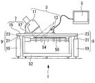
기판 외관 검사 장치(1)는, 도 1 및 도 2에 나타낸 바와 같이, 제조 라인(52) 상으로 반송되어 오는 기판(50)의 표면의 외관을 관찰하는 검사 장치 유닛(3)과, 검사 장치 유닛(3)에 의해 촬영된 화상을 표시하는 모니터(5)와, 검사 장치 유닛(3)을 기판(50)의 반송 방향과 교차하는 방향으로 이동시키는 제1 이동 기구(7)와, 검사 장치 유닛(3)을 기판(50)의 반송 방향으로 이동시키는 제2 이동 기구(9)를 구비하고 있다.The board | substrate external
검사 장치 유닛(3)은, 도 3에 나타낸 바와 같이, 기판(50)의 표면에 조사하는 조명광으로서 산란광과 수속광을 발생하는 조명 장치(조명부)(11)와, 조명 장 치(11)로부터 발해지고 기판(50)의 표면에서 반사된 반사광에 의한 기판(50)의 표면의 상을 촬영하는 카메라(촬영부)(13)를 구비하고 있다. 이들 조명 장치(11)와 카메라(13)는, 후술하는 제1 이동 기구(7)에 장착되어 있다.As shown in FIG. 3, the
조명 장치(11)는, 제조 라인(52) 상의 기판(50)의 표면에 대하여, 조명광의 광축을 소정의 경사 각도로 경사지게 배치되어 있다. 또한, 조명 장치(11)로부터는, 도 3에 나타낸 바와 같이, 수속광이 출사되도록 되어 있다.The
그리고, 조명 장치(11)로부터는, 산란광 또는 수속광 중 어느 한쪽이 출사 되면 된다.And either of scattered light or convergent light may be emitted from the
또한, 바람직하게는, 조명 장치(11)는, 광원으로부터 출사된 조명광을 수속시키는 프레넬 렌즈(Fresnel lens)와, 투명 상태와 산란 상태로 전환되는 투과형 액정 산란판을 구비한다. 투과형 액정 산란판을 기판(50)의 검사 조건에 따라 투명 상태와 산란 상태로 전환시킨다.In addition, the illuminating
카메라(13)는, 예를 들면, CCD 등 2차원 화상을 취득 가능한 카메라이며, 정지 화상 또는 동영상 중 적어도 한쪽의 화상을 취득할 수 있다. 카메라(13)는, 제조 라인(52) 상의 기판(50)의 표면에 대하여, 그 광축을 소정의 경사 각도로 경사지게 하고, 또한 조명 장치(11)에 의한 조명 범위의 중심에 광축을 일치시키도록 배치되어 있다.The
카메라(13)는, 조명 범위의 중심을 회전 지점으로 하여 XY의 2차원 방향, 또는 시점 위치가 되는 카메라(13)의 촬영 위치를 회전 지점으로 하여 XY의 2차원 방향으로 회전 이동 가능하도록 지지되고, 죠이스틱 등의 조작부를 관찰자가 조작함 으로써, 카메라(13)를 원하는 촬영 위치 및 촬영 각도로 원격 조작시켜도 된다.The
또한, 카메라(13)는 줌 기구를 구비하고 있다. 이 줌 기구에 의해 검출된 결함을 확대하고, 이 결함이 카메라(13)의 시야 내에 들어가도록, 촬영 위치를 회전 지점으로 하여 카메라(13)를 XY의 2차원 방향으로 회전 이동시킬 수도 있다.Moreover, the
또한, 카메라(13)는, 조명 장치(11)로부터의 조명광의, 기판(50)의 표면에서 정반사된 수속광의 범위 밖으로 위치하도록 지지되어 있다. 그리고, 선명한 화상을 얻기 위하여, 수속광의 범위 밖이면서, 또한 수속광의 근방에 카메라(13)를 설치하는 것이 바람직하다.Moreover, the
모니터(5)는, 도 2에 나타낸 바와 같이, 카메라(13)와 접속되고, 카메라(13)에 의해 촬영된 기판(50)의 표면의 화상이 표시되도록 되어 있다. 또한, 모니터(5)는, 카메라(13)에 의해 촬영된 조명 범위의 매크로 상과 확대된 결함상을 기억하는 기억부(도시 생략)를 구비하고 있다.As shown in FIG. 2, the
제1 이동 기구(7)는, 제조 라인(52)의 반송 방향(Y 방향)과 교차하는 폭 방향(X 방향)으로 걸쳐서 설치된 제1 레일(15)과, 제1 레일(15) 상으로 이동 가능하게 지지되는 제1 슬라이더(17)와, 제1 슬라이더(17)를 제1 레일(15)을 따라 구동시키는, 예를 들면, 리니어 모터 등의 직접 구동 기구로 이루어지는 제1 구동 장치(도시 생략)를 구비하고 있다.The
제1 슬라이더(17)는, 카메라(13)에 의해 표시되는 화상을 연속시켜서 모니터(5) 상에 비추는 것에 의해 얻어지는 동영상이, 관찰자에 의해 기판(50) 상의 결함을 확인할 수 있는 정도의 움직임이 되는 일정한 속도로 이동시키고, 관찰자가 결함을 발견할 때 정지시키도록 해도 된다. 이 경우, 관찰자가 결함으로 판정하면, 카메라(13)에 의해 촬영된 화상을 정지 화상으로서 보존하고, 또한 이 정지 화상에 대한 기판(50) 상의 좌표 위치를 구하고, 이것을 위치 정보로서 보존한다. 이와 같이, 관찰자가 결함으로서 판정한 정지 화상과 위치 정보만을 보존함으로써, 나중에 판정 결과를 재확인·검정할 때의 데이터로서 활용할 수 있다.The
제1 레일(15)은 한쌍의 평행하는 레일 부재이다. 제1 레일(15)은, 제조 라인(52)의 위쪽에 위치하도록, 길이 방향의 양 단부를 각각 후술하는 제2 이동 기구(9)에 지지되어 있다. 또한, 제1 레일(15)은, 한쌍의 레일 부재가, 제조 라인(52)의 반송 방향으로 간격을 두고 배치되고, 제1 슬라이더(17)의 양 단부를 각각 지지하도록 되어 있다.The
제1 슬라이더(17)는, 직사각형의 개구부를 가지는 프레임형으로 형성되고, X 방향으로 대치하는 양쪽 프레임부에 조명 장치(11) 및 카메라(13)가 탑재되어 있다. 이에 따라, 제1 슬라이더(17)의 하방으로 반송되는 기판(50)에 대하여, 조명 장치(11)로부터의 조명광이 개구부를 통과하여 기판(50)에 조사되고, 또한 기판(50)의 표면으로부터의 반사광이 개구부를 통과하여 카메라(13)에 입사되고, 기판(50)의 표면의 상이 표시되도록 되어 있다. 또한, 제1 슬라이더(17)를 제1 레일(15)을 따라 구동시키면, 조명 장치(11)와 카메라(13)가 제조 라인(52)의 반송 방향과 직교하는 방향으로 일체적으로 이동하도록 되어 있다.The
제2 이동 기구(9)는, 제조 라인(52)의 반송 방향을 따라 배치되는 한쌍의 베이스(19)와, 베이스(19) 상에 장착되는 제2 레일(21)과, 제2 레일(21) 상으로 이동 가능하게 지지되는 제2 슬라이더(23)와, 제2 슬라이더(23)를 제2 레일(21)을 따라 이동시키는, 예를 들면, 리니어 모터 등의 직선 구동 기구로 이루어지는 제2 구동 장치(도시 생략)를 구비하고 있다.The 2nd moving
베이스(19)는, 제조 라인(52)의 기판 반송로에 평행하게 그 양측에 배치된다. 또한, 베이스(19)는, 제조 라인(52)의 기판 반송 높이에 맞추어서 상하로 위치 조절 가능하게 되어 있다. 이에 따라, 기판 반송로를 구성하는 컨베이어(54)에 의해 반송되는 기판(50)에 대하여 카메라(13)의 초점 위치가 최적이 되도록, 검사 장치 유닛(3)의 높이를 조절할 수 있도록 되어 있다.The
제2 레일(21)은, 한쌍의 평행한 레일 부재이다. 제2 레일(21)은, 베이스(19)의 상단면을 따라 제조 라인(52)의 반송 방향과 평행하게 장착되어 있다.The
제2 슬라이더(23)는, 제1 레일(15) 사이의 폭과 같은 정도의 길이의 판형 부재이며, 제1 레일(15)의 길이 방향의 양 단부가 각각 제2 슬라이더(23)에 장착되어 있다.The
즉, 제1 이동 기구(7)와 제2 이동 기구(9)는, 서로 직교하도록 조합되고, 검사 장치 유닛(3)을 XY 방향의 2차원 방향으로 이동 가능한 XY 스테이지로 구성되어 있다. 이에 따라, 검사 장치 유닛(3)은, 제1 이동 기구(7)의 작동에 의해 제조 라인(52)의 반송 방향과 교차하는 방향으로 이동 가능하게 되면서, 제2 이동 기구(9)의 작동에 의해 제조 라인(52)의 반송 방향으로 소정 피치로 이동시킴으로써, 기판(50)의 전체면에 대하여 소정 피치마다 좌우로 사행(蛇行)한다.That is, the 1st moving
또한, 본 실시예에 따른 기판 외관 검사 장치(1)는, 예를 들면, 제1 레 일(15)과 제2 레일(21)에 각각 X 스케일, Y 스케일을 설치하고, 이들 스케일에 의해 판독된 검사 장치 유닛(3)의 XY 좌표에 기초하여, 모니터(5) 상에 표시되어 있는 화상의 중심 위치를, 기판(50) 상의 좌표와 대응시켜 기억부에 기억한다. 또한, 이 화상 내의 결함의 중심 위치를 포인터(도시 생략)로 지정함으로써, 결함의 위치 좌표(즉, X 방향 거리와 Y 방향 거리)를 산출하고, 기판(50)의 좌표에 대응시켜 기억부에 기억해도 된다.In addition, in the board | substrate
이와 같이 구성된 본 실시예에 따른 기판 외관 검사 장치(1)의 작용에 대하여 설명한다.The function of the board | substrate
본 실시예에 따른 기판 외관 검사 장치(1)에 의해, 제조 라인(52) 상을 반송되는 기판(50)을 검사하기 위해서는, 먼저, 기판 외관 검사 장치(1)를 제조 라인(52)의 임의의 위치에 설치한다.In order to test the board |
예를 들면, 도 4에 나타낸 바와 같이, 제1 제조 장치(56)로부터 제2 제조 장치(58)에 기판(50)을 반송하는 제조 라인(52)이며, 기판 반송로가 약 90° 절곡된 코너 부분을 가지는 것에서는, 설치 위치 60, 62 및 64와 같이 기판(50)을 직선 이동시키는 직선 반송 라인의 위치에, 제1 레일(15)이 제조 라인(52)의 기판 반송 방향과 교차하는 방향으로 걸쳐서 설치되도록, 베이스(19)를 제조 라인(52)의 양 사이드에 배치한다.For example, as shown in FIG. 4, it is a
그리고, 예를 들면, 기판(50) 상에 레지스트를 도포하는 제조 장치로부터 반출된 기판(50)은, 제조 라인(52)의 컨베이어(54)에 의해, 다음 제조 단계에 설치된 제조 장치로 반송된다. 여기서, 반송되어 오는 기판(50)은, 기판 외관 검사 장 치(1)의 검사 영역 내에서 일단 정지된다. 검사 장치 유닛(3)을, 도 1의 화살표 A에 나타낸 바와 같이 래스터 스캔(raster scan)하도록 이동시켜서, 기판(50)의 표면의 전체에 걸쳐 조명 장치(11)로부터 조명광을 조사하고, 카메라(13)와 기판(50)의 표면의 상을 촬영한다.For example, the board |
예를 들면, 도 4에 나타낸 바와 같이, 각 제조 장치(56, 58)의 반출 측 또는 반입 측이 되는 설치 위치(60, 64)에 기판 외관 검사 장치(1)를 설치한 경우, 기판 반송로가 되는 컨베이어(54)의 간극에 설치한 위치 검출 센서(도시 생략)에 의해, 기판(50)이 검사 영역 내에 반입된 것이 검지되면 컨베이어(54)의 구동을 정지하고, 설치 위치(60, 64)에 설치된 기판 외관 검사 장치(1)의 검사 영역 내에 기판(50)을 정지시킨다. 그리고, 제1 이동 기구(7)의 작동에 의해, 검사 장치 유닛(3)을 제조 라인(52)의 기판 반송 방향과 직교하는 방향으로 왕복 이동시킴으로써, 기판(50)의 단변 방향 전체에 걸친 상세한 관찰을 행할 수 있다.For example, as shown in FIG. 4, when the board | substrate
또한, 제2 이동 기구(9)의 작동에 의해, 제1 이동 기구(7)를 제조 라인(52)의 반송 방향으로 조명 범위의 조사 폭보다 약간 짧은 폭 피치로 이동시킴으로써, 기판(50)의 장변 방향 전체에 걸친 상세한 관찰을 행할 수 있다.In addition, by operating the
또한, 도 4에 나타낸 설치 위치(62)에 기판 외관 검사 장치(1)를 설치한 경우, 반송되어 오는 기판(50)은, 설치 위치(60)에 대하여 약 90° 회전된 상태로 반송되게 된다. 즉, 기판(50)은, 반송 라인의 코너 부분에서 방향이 바꾸어지지 않고 이동 방향만 약 90° 바뀌어져서 반송된다. 따라서, 설치 위치(62)의 기판 외관 검사 장치(1)에 대해서는, 설치 위치(60)에서의 기판 외관 검사 장치(1)에 대한 기판(50)의 방향이 90° 회전된 방향으로 반송된다.In addition, when the board | substrate
다음에, 제조 라인(52)의 설치 위치(62) 상에 기판(50)을 정지시킨다. 그리고, 제1 이동 기구(7)의 작동에 의해, 반송되어 오는 직사각형의 기판(50)에 대하여, 검사 장치 유닛(3)을 제조 라인(52)의 기판 반송 방향과 직교하는 방향으로 왕복 이동시킴으로써, 기판(50)의 장변 방향 전체에 걸친 상세한 관찰을 행할 수 있다.Next, the
또한, 제2 이동 기구(9)의 작동에 의해, 제1 이동 기구(7)를 제조 라인(52)의 반송 방향으로 조명 범위의 조사 폭보다 약간 짧은 피치로 이동시킴으로써, 기판(50)의 단변 방향 전체에 걸친 상세한 관찰을 행할 수 있다.Moreover, the short side of the board |
이에 따라, 기판(50)의 표면에 형성된 직사각형의 패턴의 배열 방향에 대하여, 설치 위치(60)와 설치 위치(62)에서 약 90° 상이한 방향으로부터 조명하여 촬영을 행할 수 있고, 기판(50)의 표면의 결함을 보다 상세하게 검사할 수 있다.Thereby, with respect to the arrangement direction of the rectangular pattern formed on the surface of the board |
이와 같이 하여, 카메라(13)에 의해 전면 주사된 기판(50)의 표면의 화상은, 모니터(5) 상에 표시되고, 관찰자의 육안 관찰에 의해 기판(50)의 외관 검사가 행해진다. 따라서, 기판(50)이 대형화되어도, 기판(50) 전체의 상세한 검사를 용이하게 행할 수 있다.In this way, an image of the surface of the
이 경우에, 도 3에 나타낸 바와 같이, 카메라(13)가, 기판(50)으로부터 반사되는 정반사광의 광속의 범위 밖으로 위치하도록 지지되어 있으므로, 카메라(13)의 조명광이 입사하여 포화되지 않고, 고정밀도의 화상을 얻을 수 있다. 따라서, 관찰자는, 모니터(5) 화상 전체에 표시된 기판(50)을 양호하게 관찰할 수 있다.In this case, as shown in FIG. 3, since the
또한, 기억부에는, 모니터(5) 상에 표시되어 있는 화상의 중심 위치(25)와 결함(27)의 위치가 기판(50) 상의 좌표와 대응되어 기억되므로, 이 결함(27)의 좌표를, 예를 들면, 마이크로 관찰 장치 등의 별도 검사 장치에서 판독함으로써, 리뷰 검사를 행할 수 있다.In addition, since the position of the
이상 설명한 바와 같이, 본 실시예에 따른 기판 외관 검사 장치(1)에 의하면, 제조 라인(52)의 기판 반송 방향과 직교하는 폭 방향으로 걸쳐서 설치하는 것만으로, 기존의 제조 라인의 기판 반송 공간에 용이하게 설치할 수 있고, 또한 기판(50)을 제조 라인(52) 밖으로 취출하지 않고 제조 라인 내에서 기판(50)의 매크로 검사를 행할 수 있다.As explained above, according to the board | substrate
따라서, 제조 라인(52)의 기판 반송로에서, 모니터(5) 상에 표시된 기판(50)의 표면의 화상에 의해 매크로 검사를 행함으로써, 종래와 같이 제조 라인 밖으로 기판을 반송하는 기판 취출 기구 등의 별도의 장치가 불필요하고, 택트 타임의 단축을 도모할 수 있다. 또한, 제조 라인(52)의 위쪽의 공간을 유효하게 활용하고, 제조 설비의 컴팩트화를 도모할 수 있다. 또한, 기존의 제조 라인(52)의 기판 반송로를 따라 기판 외관 검사 장치(1)를 배치하므로, 이미 구축된 제조 라인(52)에 기판 외관 검사 장치(1)를 간단하게 나중에 설치할 수도 있다.Therefore, in the substrate conveyance path of the
그리고, 본 실시예에 따른 기판 외관 검사 장치(1)는, 제1 이동 기구(7) 및 제2 이동 기구(9)를 구비하는 것으로 하였으나, 이에 대신하여, 제1 이동 기구(7)만을 구비하고, 제2 이동 기구(9)를 기판(50)을 반송하는 컨베이어에 겸용시킴으로써, 기판(50)의 반송 방향 전체에 걸친 상세한 관찰을 행할 수 있다. 또한, 제2 이동 기구(9)를 생략함으로써, 기판 외관 검사 장치(1)를 더욱 컴팩트화할 수 있다.In addition, although the board | substrate
또한, 예를 들면, 본 실시예에 따른 기판 외관 검사 장치(1)는, 모니터(5)에 의한 육안 관찰 검사를 행하는 것으로 하였으나, 나아가서는 기판 외관 검사 장치(1)의 하류 측에, 상류 측에서 검출된 결함을 더 확대하여 상세한 검사를 행하는 마이크로 검사 장치를 구비한 것으로 하고, 매크로 검사로 결함의 좌표를 얻어, 이 결함의 위치 정보에 기초하여, 마이크로 검사 장치에 의한 결함의 상세 검사를 행하여도 된다.In addition, for example, although the board | substrate
[제2 실시예]Second Embodiment
다음에, 본 발명의 제2 실시예에 따른 기판 외관 검사 장치(31)에 대하여, 도 5 및 도 6을 참조하여 설명한다.Next, a substrate
본 실시예에 따른 기판 외관 검사 장치(31)는, 검사 장치 유닛(3)이 가이드(회전 기구)(33)를 구비한다.In the board | substrate external
이하, 제1 실시예에 따른 기판 외관 검사 장치(1)와 구성을 공통으로 하는 개소에는, 동일한 부호를 부여하여 설명을 생략한다.Hereinafter, the same code | symbol is attached | subjected to the location which has a structure common to the board | substrate
가이드(33)는, 조명 장치(11)로부터 조사하는 조명광의 기판(50) 상에서의 조사 범위의 중심 위치(35)에 카메라(13)의 광축이 항상 향하도록 카메라(13)를 회전시키는 것이다. 구체적으로는, 가이드(33)는 반원호형의 레일이며, 카메라(14)는 가이드(33)를 따라 이동 가능하게 장착되어 있다.The
또한, 가이드(33)는, 카메라(13)의 광축과 기판(50)에 대한 각도가 서서히 작아지도록, 조명광의 반사 방향 측에 기판(50)에 대하여 약 45° 각도로 경사지게 하여 설치되어 있다. 이에 따라, 도 6에 나타낸 바와 같이, 중심 위치(35) 주위에 약 180°범위 내에서, 카메라(13)를 약 45° 경사진 상태로 회전 이동시킬 수 있도록 되어 있다.The
이와 같이 함으로써, 예를 들면, 카메라 위치 13A, 13B 및 13C와 같이 카메라(13)의 시점을 바꾸면서 기판(50)의 검사를 행할 수 있다. 따라서, 관찰자가 기판(50)에 대하여 목을 좌우로 기울이게 하는 것과 같은, 육안 관찰자에 의한 직시(直視)에 가까운 관찰을 행할 수 있다.By doing in this way, the board |
그리고, 도 7에 나타낸 바와 같이, 카메라(13)의 광축을 조명광의 반사 축에 대하여 기판(50)에 대한 각도를 임의로 바꿀 수 있는 제2 가이드(37)를 가이드(33)에 장착하고, 카메라(13)의 높이 방향의 이동을 가이드해도 된다.As illustrated in FIG. 7, the
도 6 및 도 7에 나타낸 바와 같이, 카메라(13)를 조명광의 조사 범위의 중심 위치를 회전 지점으로 하여 좌우 방향과 전후 방향으로 회전시킴으로써, 기판(50)에 대한 다(多) 방향으로부터 시점을 변경한 카메라(13)에 의한 촬영이 가능해지고, 기판(50) 상의 결함 검출의 정밀도를 높일 수 있다.As shown in FIG. 6 and FIG. 7, the
이상, 본 발명의 각 실시예에 대하여 도면을 참조하여 상세하게 설명하였지만, 구체적인 구성은 이러한 실시예에 한정되지 않고, 본 발명의 요지를 벗어나지 않는 범위의 설계 변경 등도 포함된다.As mentioned above, although each Example of this invention was described in detail with reference to drawings, a specific structure is not limited to this Example, The design change etc. of the range which do not deviate from the summary of this invention are included.
예를 들면, 전술한 각 실시예에 따른 기판 반송 장치(1, 31)의 베이스(19)를 제조 라인(52)의 폭 방향으로 걸쳐진 형상으로 형성해도 된다. 이와 같이 함으로 써, 예를 들면, 도 4의 설치 위치와 같이 제조 라인(52)의 코너(66, 68)에 기판 반송 장치(1, 31)를 설치할 수도 있다. 따라서, 종래에는 데드 스페이스(dead space)가 되는 제조 라인(52)의 코너 부분의 기판 반입 측과 기판 반출 측에 기판 외관 검사 장치(1, 31)를 설치할 수 있게 되고, 제조 라인(52)의 형상에 좌우되지 않고 기판 외관 검사 장치(1, 31)를 구축할 수 있으며, 제조 라인(52) 위쪽의 공간을 한층 더 유효하게 활용하고, 제조 설비의 컴팩트화를 도모할 수 있다.For example, you may form the
또한, 검사 장치 유닛(3)의 조명 주사 영역이 되는 검사 영역을 롤러 컨베이어로부터 기판(50)을 소정의 높이로 부상시키는 에어 부상 스테이지가 대신할 수도 있다. 이 경우, 기판(50)의 부상 높이를 일정하게 유지하기 위하여 스테이지 상면에 에어를 분출시키는 분출구멍과, 에어를 흡인하는 흡인구멍을 설치하고, 에어의 분출압과 흡인압에 의해 기판(50)을 일정한 높이로 부상시킨다. 이와 같이, 기판(50)을 부상시킴으로써, 기판(50)을 완전히 비접촉으로 지지할 수 있으므로, 마더 글래스와 같이 투명한 기판의 배면 아래의 배경에 기인하는 영향을 저감시킬 수 있고, 의사(擬似) 결함에 의한 오검출을 방지할 수 있다.In addition, the air floating stage which raises the board |
도 1은 본 발명의 제1 실시예에 따른 기판 외관 검사 장치를 위쪽으로부터 본 개략적인 구성도이다.1 is a schematic configuration view of a substrate visual inspection apparatus according to a first embodiment of the present invention as seen from above.
도 2는 도 1의 기판 외관 검사 장치의 측면도이다.FIG. 2 is a side view of the substrate appearance inspection apparatus of FIG. 1. FIG.
도 3은 도 1의 기판 외관 검사 장치의 검사 장치 유닛을 나타내는 개략적인 도면이다.FIG. 3 is a schematic view showing an inspection apparatus unit of the substrate appearance inspection apparatus of FIG. 1.
도 4는 기판의 제조 라인을 나타내는 개략적인 도면이다.4 is a schematic diagram illustrating a manufacturing line of a substrate.
도 5는 본 발명의 제2 실시예에 따른 기판 외관 검사 장치의 가이드를 나타내는 개략적인 도면이다.5 is a schematic diagram illustrating a guide of a substrate appearance inspection apparatus according to a second exemplary embodiment of the present invention.
도 6은 도 5의 기판 외관 검사 장치의 검사 장치 유닛을 나타낸 도면이다.It is a figure which shows the inspection apparatus unit of the board | substrate visual inspection apparatus of FIG.
도 7은 도 5의 가이드의 변형예를 나타내는 개략적인 도면이다.7 is a schematic diagram illustrating a modification of the guide of FIG. 5.
[부호의 설명][Description of the code]
1, 31: 기판 외관 검사 장치1, 31: substrate appearance inspection device
5: 모니터5: monitor
7: 제1 이동 기구7: first moving mechanism
9: 제2 이동 기구9: second moving mechanism
11: 조명 장치(조명부)11: lighting device (lighting)
13: 카메라(촬영부)13: Camera (photographer)
15: 제1 레일15: first rail
17: 제1 슬라이더17: first slider
21: 제2 레일21: second rail
23: 제2 슬라이더23: second slider
33: 가이드(회전 기구)33: guide (rotary mechanism)
50: 기판50: substrate
52: 제조 라인52: manufacturing line
Claims (9)
Applications Claiming Priority (2)
| Application Number | Priority Date | Filing Date | Title |
|---|---|---|---|
| JPJP-P-2007-00178772 | 2007-07-06 | ||
| JP2007178772A JP2009014617A (en) | 2007-07-06 | 2007-07-06 | Substrate visual inspection apparatus |
Publications (1)
| Publication Number | Publication Date |
|---|---|
| KR20090004636A true KR20090004636A (en) | 2009-01-12 |
Family
ID=40213265
Family Applications (1)
| Application Number | Title | Priority Date | Filing Date |
|---|---|---|---|
| KR1020080063316A KR20090004636A (en) | 2007-07-06 | 2008-07-01 | Substrate surface inspection apparatus |
Country Status (4)
| Country | Link |
|---|---|
| JP (1) | JP2009014617A (en) |
| KR (1) | KR20090004636A (en) |
| CN (1) | CN101339143A (en) |
| TW (1) | TW200909798A (en) |
Cited By (1)
| Publication number | Priority date | Publication date | Assignee | Title |
|---|---|---|---|---|
| KR20190051031A (en) * | 2016-09-30 | 2019-05-14 | 상하이 마이크로 일렉트로닉스 이큅먼트(그룹) 컴퍼니 리미티드 | How to Detect Particles in the Panel |
Families Citing this family (25)
| Publication number | Priority date | Publication date | Assignee | Title |
|---|---|---|---|---|
| KR101080216B1 (en) * | 2009-02-17 | 2011-11-09 | (주)글로벌 텍 | Apparatus for inspecting glass edge and method for inspecting glass edge using thereof |
| JP5274389B2 (en) * | 2009-06-18 | 2013-08-28 | 株式会社アルバック | Maintenance device and discharge device |
| TW201118027A (en) * | 2009-11-30 | 2011-06-01 | Schmid Yaya Technology Co Ltd | Chip transporting machine table |
| US8432540B2 (en) * | 2010-03-31 | 2013-04-30 | Cooper S.K. Kuo | Support mechanism for inspection systems |
| CN102680495B (en) * | 2011-03-15 | 2016-09-07 | 上海赫立电子科技有限公司 | Automatic optical detection device and method |
| KR20140022064A (en) * | 2011-05-10 | 2014-02-21 | 아사히 가라스 가부시키가이샤 | Method for inspecting minute defect of translucent board-like body, and apparatus for inspecting minute defect of translucent board-like body |
| CN102621149B (en) * | 2012-03-21 | 2015-07-22 | 深圳市华星光电技术有限公司 | Substrate detection device and method |
| US20130248692A1 (en) * | 2012-03-21 | 2013-09-26 | Shenzhen China Star Optoelectronics Technology Co Ltd. | Detecting apparatus and method for substrate |
| CN102636498B (en) * | 2012-03-22 | 2014-04-16 | 深圳市华星光电技术有限公司 | Detection device and detection method for glass substrate |
| CN102866167A (en) * | 2012-10-19 | 2013-01-09 | 深圳市劲拓自动化设备股份有限公司 | Offline detecting system and method of circuit board |
| CN104568973A (en) * | 2015-02-09 | 2015-04-29 | 京东方科技集团股份有限公司 | Device and method for detecting substrate |
| CN105115979A (en) * | 2015-09-09 | 2015-12-02 | 苏州威盛视信息科技有限公司 | Image mosaic technology-based PCB working sheet AOI (Automatic Optic Inspection) method |
| JP6587211B2 (en) * | 2015-12-17 | 2019-10-09 | 日本電気硝子株式会社 | Manufacturing method of glass plate |
| KR101751801B1 (en) * | 2016-05-18 | 2017-06-29 | 한국기계연구원 | Defect inspecting device for substrate and inspecting method using the same |
| CN106862097A (en) * | 2017-03-27 | 2017-06-20 | 江苏凯伦铝业有限公司 | Photovoltaic module aluminium frame full-automatic detection apparatus |
| FR3066821B1 (en) * | 2017-05-24 | 2019-07-12 | Areva Np | DEVICE FOR DETECTING A DEFECT ON A SURFACE BY MULTIDIRECTIONAL LIGHTING |
| CN107843991A (en) * | 2017-09-05 | 2018-03-27 | 努比亚技术有限公司 | Detection method, system, terminal and the computer-readable recording medium of screen light leak |
| JP6795479B2 (en) * | 2017-09-25 | 2020-12-02 | 株式会社Screenホールディングス | Inspection equipment and inspection method |
| CN107526196A (en) * | 2017-09-27 | 2017-12-29 | 武汉华星光电技术有限公司 | Glass base-board load-bearing device and detection device |
| CN107907549A (en) * | 2017-11-13 | 2018-04-13 | 武汉华星光电半导体显示技术有限公司 | Inspecting substrate equipment and substrate inspecting method |
| JP2019158500A (en) * | 2018-03-12 | 2019-09-19 | オムロン株式会社 | Visual inspection system, image processing device, imaging device, and inspection method |
| KR102374037B1 (en) * | 2018-06-29 | 2022-03-11 | 캐논 톡키 가부시키가이샤 | Subtrate inspection system, manufacturing system of electronic device, subtrate inspection method, and manufacturing method of electronic device |
| CN110783223B (en) * | 2018-07-24 | 2024-04-16 | 泰克元有限公司 | Imaging device for electronic component processing equipment |
| CN113945491A (en) * | 2021-09-01 | 2022-01-18 | 郑州旭飞光电科技有限公司 | Glass substrate surface particle detection system |
| CN114994062B (en) * | 2022-08-05 | 2023-03-14 | 深圳市倍捷锐生物医学科技有限公司 | Method and system for detecting surface quality of material and storage medium |
Family Cites Families (7)
| Publication number | Priority date | Publication date | Assignee | Title |
|---|---|---|---|---|
| JPH10300446A (en) * | 1997-04-30 | 1998-11-13 | Nissan Motor Co Ltd | Surface defect inspection device |
| JP2000039564A (en) * | 1998-07-24 | 2000-02-08 | Sony Corp | Enlarging observation device |
| JP4744665B2 (en) * | 2000-03-15 | 2011-08-10 | オリンパス株式会社 | Substrate inspection apparatus and substrate inspection system |
| JP2003075294A (en) * | 2001-09-05 | 2003-03-12 | Toray Ind Inc | Method for inspecting substrate |
| WO2003027652A1 (en) * | 2001-09-21 | 2003-04-03 | Olympus Corporation | Defect inspection apparatus |
| JP2003262593A (en) * | 2002-03-08 | 2003-09-19 | Mitsubishi Rayon Co Ltd | Apparatus and method for detection of defect |
| JP4243837B2 (en) * | 2003-03-14 | 2009-03-25 | 株式会社日立ハイテクノロジーズ | Transparent substrate surface inspection method and inspection apparatus |
-
2007
- 2007-07-06 JP JP2007178772A patent/JP2009014617A/en active Pending
-
2008
- 2008-06-13 TW TW097122167A patent/TW200909798A/en unknown
- 2008-07-01 KR KR1020080063316A patent/KR20090004636A/en not_active Application Discontinuation
- 2008-07-03 CN CNA2008101281276A patent/CN101339143A/en active Pending
Cited By (1)
| Publication number | Priority date | Publication date | Assignee | Title |
|---|---|---|---|---|
| KR20190051031A (en) * | 2016-09-30 | 2019-05-14 | 상하이 마이크로 일렉트로닉스 이큅먼트(그룹) 컴퍼니 리미티드 | How to Detect Particles in the Panel |
Also Published As
| Publication number | Publication date |
|---|---|
| TW200909798A (en) | 2009-03-01 |
| CN101339143A (en) | 2009-01-07 |
| JP2009014617A (en) | 2009-01-22 |
Similar Documents
| Publication | Publication Date | Title |
|---|---|---|
| KR20090004636A (en) | Substrate surface inspection apparatus | |
| KR101305262B1 (en) | Substrate inspection apparatus | |
| TWI264532B (en) | Substrate inspection device | |
| US7016465B2 (en) | X-ray CT apparatus | |
| JP5198535B2 (en) | Glass substrate cut surface inspection system | |
| KR100827342B1 (en) | Coordinates detection apparatus and subject inspection apparatus | |
| US6432800B2 (en) | Inspection of defects on the circumference of semiconductor wafers | |
| JP2006234553A (en) | Visual inspection device and visual inspection method | |
| JP2009014617A5 (en) | ||
| JP4706356B2 (en) | Screw shape measuring device | |
| JP2001004341A (en) | Wafer shape measuring device | |
| JP2008046109A (en) | Flaw inspection device of substrate, and manufacturing method of substrate | |
| CN101048058B (en) | A component placement unit as well as a component placement device comprising such a component placement unit | |
| KR101758647B1 (en) | Inspection apparatus of non-planar display panel | |
| JP6590429B1 (en) | Confocal microscope and imaging method thereof | |
| JP2008292494A (en) | Substrate-inspecting device | |
| JP2000275594A (en) | Substrate inspecting device | |
| JP2009079915A (en) | Method and device for measuring micro-dimension | |
| KR101234954B1 (en) | Second-dimensional Coordinate Measuring Instrument | |
| JP2008170254A (en) | Substrate inspection system | |
| JP2016205985A (en) | measuring device | |
| JP2003295066A (en) | Microscope apparatus | |
| JP6879484B2 (en) | Image acquisition device, exposure device, and image acquisition method | |
| JP2008241662A (en) | Image stabilizing device | |
| KR100672166B1 (en) | Line width measuring method |
Legal Events
| Date | Code | Title | Description |
|---|---|---|---|
| WITN | Application deemed withdrawn, e.g. because no request for examination was filed or no examination fee was paid |