KR20080015724A - 몰딩된 리드 부착물을 갖는 플라스틱 오버몰딩된 패키지들 - Google Patents
몰딩된 리드 부착물을 갖는 플라스틱 오버몰딩된 패키지들 Download PDFInfo
- Publication number
- KR20080015724A KR20080015724A KR1020070079026A KR20070079026A KR20080015724A KR 20080015724 A KR20080015724 A KR 20080015724A KR 1020070079026 A KR1020070079026 A KR 1020070079026A KR 20070079026 A KR20070079026 A KR 20070079026A KR 20080015724 A KR20080015724 A KR 20080015724A
- Authority
- KR
- South Korea
- Prior art keywords
- lead
- overmold
- package
- mcm
- devices
- Prior art date
Links
Images


Classifications
-
- H—ELECTRICITY
- H01—ELECTRIC ELEMENTS
- H01L—SEMICONDUCTOR DEVICES NOT COVERED BY CLASS H10
- H01L23/00—Details of semiconductor or other solid state devices
- H01L23/02—Containers; Seals
-
- H—ELECTRICITY
- H01—ELECTRIC ELEMENTS
- H01L—SEMICONDUCTOR DEVICES NOT COVERED BY CLASS H10
- H01L23/00—Details of semiconductor or other solid state devices
- H01L23/28—Encapsulations, e.g. encapsulating layers, coatings, e.g. for protection
- H01L23/31—Encapsulations, e.g. encapsulating layers, coatings, e.g. for protection characterised by the arrangement or shape
- H01L23/3107—Encapsulations, e.g. encapsulating layers, coatings, e.g. for protection characterised by the arrangement or shape the device being completely enclosed
- H01L23/3121—Encapsulations, e.g. encapsulating layers, coatings, e.g. for protection characterised by the arrangement or shape the device being completely enclosed a substrate forming part of the encapsulation
-
- H—ELECTRICITY
- H01—ELECTRIC ELEMENTS
- H01L—SEMICONDUCTOR DEVICES NOT COVERED BY CLASS H10
- H01L23/00—Details of semiconductor or other solid state devices
- H01L23/34—Arrangements for cooling, heating, ventilating or temperature compensation ; Temperature sensing arrangements
- H01L23/42—Fillings or auxiliary members in containers or encapsulations selected or arranged to facilitate heating or cooling
- H01L23/433—Auxiliary members in containers characterised by their shape, e.g. pistons
- H01L23/4334—Auxiliary members in encapsulations
-
- H—ELECTRICITY
- H01—ELECTRIC ELEMENTS
- H01L—SEMICONDUCTOR DEVICES NOT COVERED BY CLASS H10
- H01L24/00—Arrangements for connecting or disconnecting semiconductor or solid-state bodies; Methods or apparatus related thereto
- H01L24/93—Batch processes
- H01L24/95—Batch processes at chip-level, i.e. with connecting carried out on a plurality of singulated devices, i.e. on diced chips
- H01L24/97—Batch processes at chip-level, i.e. with connecting carried out on a plurality of singulated devices, i.e. on diced chips the devices being connected to a common substrate, e.g. interposer, said common substrate being separable into individual assemblies after connecting
-
- H—ELECTRICITY
- H01—ELECTRIC ELEMENTS
- H01L—SEMICONDUCTOR DEVICES NOT COVERED BY CLASS H10
- H01L2224/00—Indexing scheme for arrangements for connecting or disconnecting semiconductor or solid-state bodies and methods related thereto as covered by H01L24/00
- H01L2224/01—Means for bonding being attached to, or being formed on, the surface to be connected, e.g. chip-to-package, die-attach, "first-level" interconnects; Manufacturing methods related thereto
- H01L2224/26—Layer connectors, e.g. plate connectors, solder or adhesive layers; Manufacturing methods related thereto
- H01L2224/31—Structure, shape, material or disposition of the layer connectors after the connecting process
- H01L2224/32—Structure, shape, material or disposition of the layer connectors after the connecting process of an individual layer connector
- H01L2224/321—Disposition
- H01L2224/32151—Disposition the layer connector connecting between a semiconductor or solid-state body and an item not being a semiconductor or solid-state body, e.g. chip-to-substrate, chip-to-passive
- H01L2224/32221—Disposition the layer connector connecting between a semiconductor or solid-state body and an item not being a semiconductor or solid-state body, e.g. chip-to-substrate, chip-to-passive the body and the item being stacked
- H01L2224/32225—Disposition the layer connector connecting between a semiconductor or solid-state body and an item not being a semiconductor or solid-state body, e.g. chip-to-substrate, chip-to-passive the body and the item being stacked the item being non-metallic, e.g. insulating substrate with or without metallisation
-
- H—ELECTRICITY
- H01—ELECTRIC ELEMENTS
- H01L—SEMICONDUCTOR DEVICES NOT COVERED BY CLASS H10
- H01L2224/00—Indexing scheme for arrangements for connecting or disconnecting semiconductor or solid-state bodies and methods related thereto as covered by H01L24/00
- H01L2224/01—Means for bonding being attached to, or being formed on, the surface to be connected, e.g. chip-to-package, die-attach, "first-level" interconnects; Manufacturing methods related thereto
- H01L2224/42—Wire connectors; Manufacturing methods related thereto
- H01L2224/47—Structure, shape, material or disposition of the wire connectors after the connecting process
- H01L2224/48—Structure, shape, material or disposition of the wire connectors after the connecting process of an individual wire connector
- H01L2224/4805—Shape
- H01L2224/4809—Loop shape
- H01L2224/48091—Arched
-
- H—ELECTRICITY
- H01—ELECTRIC ELEMENTS
- H01L—SEMICONDUCTOR DEVICES NOT COVERED BY CLASS H10
- H01L2224/00—Indexing scheme for arrangements for connecting or disconnecting semiconductor or solid-state bodies and methods related thereto as covered by H01L24/00
- H01L2224/01—Means for bonding being attached to, or being formed on, the surface to be connected, e.g. chip-to-package, die-attach, "first-level" interconnects; Manufacturing methods related thereto
- H01L2224/42—Wire connectors; Manufacturing methods related thereto
- H01L2224/47—Structure, shape, material or disposition of the wire connectors after the connecting process
- H01L2224/48—Structure, shape, material or disposition of the wire connectors after the connecting process of an individual wire connector
- H01L2224/481—Disposition
- H01L2224/48151—Connecting between a semiconductor or solid-state body and an item not being a semiconductor or solid-state body, e.g. chip-to-substrate, chip-to-passive
- H01L2224/48221—Connecting between a semiconductor or solid-state body and an item not being a semiconductor or solid-state body, e.g. chip-to-substrate, chip-to-passive the body and the item being stacked
- H01L2224/48225—Connecting between a semiconductor or solid-state body and an item not being a semiconductor or solid-state body, e.g. chip-to-substrate, chip-to-passive the body and the item being stacked the item being non-metallic, e.g. insulating substrate with or without metallisation
- H01L2224/48227—Connecting between a semiconductor or solid-state body and an item not being a semiconductor or solid-state body, e.g. chip-to-substrate, chip-to-passive the body and the item being stacked the item being non-metallic, e.g. insulating substrate with or without metallisation connecting the wire to a bond pad of the item
-
- H—ELECTRICITY
- H01—ELECTRIC ELEMENTS
- H01L—SEMICONDUCTOR DEVICES NOT COVERED BY CLASS H10
- H01L2224/00—Indexing scheme for arrangements for connecting or disconnecting semiconductor or solid-state bodies and methods related thereto as covered by H01L24/00
- H01L2224/73—Means for bonding being of different types provided for in two or more of groups H01L2224/10, H01L2224/18, H01L2224/26, H01L2224/34, H01L2224/42, H01L2224/50, H01L2224/63, H01L2224/71
- H01L2224/732—Location after the connecting process
- H01L2224/73251—Location after the connecting process on different surfaces
- H01L2224/73265—Layer and wire connectors
-
- H—ELECTRICITY
- H01—ELECTRIC ELEMENTS
- H01L—SEMICONDUCTOR DEVICES NOT COVERED BY CLASS H10
- H01L2224/00—Indexing scheme for arrangements for connecting or disconnecting semiconductor or solid-state bodies and methods related thereto as covered by H01L24/00
- H01L2224/91—Methods for connecting semiconductor or solid state bodies including different methods provided for in two or more of groups H01L2224/80 - H01L2224/90
- H01L2224/92—Specific sequence of method steps
- H01L2224/922—Connecting different surfaces of the semiconductor or solid-state body with connectors of different types
- H01L2224/9222—Sequential connecting processes
- H01L2224/92242—Sequential connecting processes the first connecting process involving a layer connector
- H01L2224/92247—Sequential connecting processes the first connecting process involving a layer connector the second connecting process involving a wire connector
-
- H—ELECTRICITY
- H01—ELECTRIC ELEMENTS
- H01L—SEMICONDUCTOR DEVICES NOT COVERED BY CLASS H10
- H01L2224/00—Indexing scheme for arrangements for connecting or disconnecting semiconductor or solid-state bodies and methods related thereto as covered by H01L24/00
- H01L2224/93—Batch processes
- H01L2224/95—Batch processes at chip-level, i.e. with connecting carried out on a plurality of singulated devices, i.e. on diced chips
- H01L2224/97—Batch processes at chip-level, i.e. with connecting carried out on a plurality of singulated devices, i.e. on diced chips the devices being connected to a common substrate, e.g. interposer, said common substrate being separable into individual assemblies after connecting
-
- H—ELECTRICITY
- H01—ELECTRIC ELEMENTS
- H01L—SEMICONDUCTOR DEVICES NOT COVERED BY CLASS H10
- H01L23/00—Details of semiconductor or other solid state devices
- H01L23/28—Encapsulations, e.g. encapsulating layers, coatings, e.g. for protection
- H01L23/31—Encapsulations, e.g. encapsulating layers, coatings, e.g. for protection characterised by the arrangement or shape
- H01L23/3107—Encapsulations, e.g. encapsulating layers, coatings, e.g. for protection characterised by the arrangement or shape the device being completely enclosed
- H01L23/3142—Sealing arrangements between parts, e.g. adhesion promotors
-
- H—ELECTRICITY
- H01—ELECTRIC ELEMENTS
- H01L—SEMICONDUCTOR DEVICES NOT COVERED BY CLASS H10
- H01L24/00—Arrangements for connecting or disconnecting semiconductor or solid-state bodies; Methods or apparatus related thereto
- H01L24/01—Means for bonding being attached to, or being formed on, the surface to be connected, e.g. chip-to-package, die-attach, "first-level" interconnects; Manufacturing methods related thereto
- H01L24/42—Wire connectors; Manufacturing methods related thereto
- H01L24/47—Structure, shape, material or disposition of the wire connectors after the connecting process
- H01L24/48—Structure, shape, material or disposition of the wire connectors after the connecting process of an individual wire connector
-
- H—ELECTRICITY
- H01—ELECTRIC ELEMENTS
- H01L—SEMICONDUCTOR DEVICES NOT COVERED BY CLASS H10
- H01L24/00—Arrangements for connecting or disconnecting semiconductor or solid-state bodies; Methods or apparatus related thereto
- H01L24/73—Means for bonding being of different types provided for in two or more of groups H01L24/10, H01L24/18, H01L24/26, H01L24/34, H01L24/42, H01L24/50, H01L24/63, H01L24/71
-
- H—ELECTRICITY
- H01—ELECTRIC ELEMENTS
- H01L—SEMICONDUCTOR DEVICES NOT COVERED BY CLASS H10
- H01L25/00—Assemblies consisting of a plurality of individual semiconductor or other solid state devices ; Multistep manufacturing processes thereof
- H01L25/03—Assemblies consisting of a plurality of individual semiconductor or other solid state devices ; Multistep manufacturing processes thereof all the devices being of a type provided for in the same subgroup of groups H01L27/00 - H01L33/00, or in a single subclass of H10K, H10N, e.g. assemblies of rectifier diodes
- H01L25/04—Assemblies consisting of a plurality of individual semiconductor or other solid state devices ; Multistep manufacturing processes thereof all the devices being of a type provided for in the same subgroup of groups H01L27/00 - H01L33/00, or in a single subclass of H10K, H10N, e.g. assemblies of rectifier diodes the devices not having separate containers
- H01L25/065—Assemblies consisting of a plurality of individual semiconductor or other solid state devices ; Multistep manufacturing processes thereof all the devices being of a type provided for in the same subgroup of groups H01L27/00 - H01L33/00, or in a single subclass of H10K, H10N, e.g. assemblies of rectifier diodes the devices not having separate containers the devices being of a type provided for in group H01L27/00
- H01L25/0655—Assemblies consisting of a plurality of individual semiconductor or other solid state devices ; Multistep manufacturing processes thereof all the devices being of a type provided for in the same subgroup of groups H01L27/00 - H01L33/00, or in a single subclass of H10K, H10N, e.g. assemblies of rectifier diodes the devices not having separate containers the devices being of a type provided for in group H01L27/00 the devices being arranged next to each other
-
- H—ELECTRICITY
- H01—ELECTRIC ELEMENTS
- H01L—SEMICONDUCTOR DEVICES NOT COVERED BY CLASS H10
- H01L2924/00—Indexing scheme for arrangements or methods for connecting or disconnecting semiconductor or solid-state bodies as covered by H01L24/00
- H01L2924/0001—Technical content checked by a classifier
- H01L2924/00014—Technical content checked by a classifier the subject-matter covered by the group, the symbol of which is combined with the symbol of this group, being disclosed without further technical details
-
- H—ELECTRICITY
- H01—ELECTRIC ELEMENTS
- H01L—SEMICONDUCTOR DEVICES NOT COVERED BY CLASS H10
- H01L2924/00—Indexing scheme for arrangements or methods for connecting or disconnecting semiconductor or solid-state bodies as covered by H01L24/00
- H01L2924/01—Chemical elements
- H01L2924/01005—Boron [B]
-
- H—ELECTRICITY
- H01—ELECTRIC ELEMENTS
- H01L—SEMICONDUCTOR DEVICES NOT COVERED BY CLASS H10
- H01L2924/00—Indexing scheme for arrangements or methods for connecting or disconnecting semiconductor or solid-state bodies as covered by H01L24/00
- H01L2924/01—Chemical elements
- H01L2924/01006—Carbon [C]
-
- H—ELECTRICITY
- H01—ELECTRIC ELEMENTS
- H01L—SEMICONDUCTOR DEVICES NOT COVERED BY CLASS H10
- H01L2924/00—Indexing scheme for arrangements or methods for connecting or disconnecting semiconductor or solid-state bodies as covered by H01L24/00
- H01L2924/01—Chemical elements
- H01L2924/01012—Magnesium [Mg]
-
- H—ELECTRICITY
- H01—ELECTRIC ELEMENTS
- H01L—SEMICONDUCTOR DEVICES NOT COVERED BY CLASS H10
- H01L2924/00—Indexing scheme for arrangements or methods for connecting or disconnecting semiconductor or solid-state bodies as covered by H01L24/00
- H01L2924/01—Chemical elements
- H01L2924/01013—Aluminum [Al]
-
- H—ELECTRICITY
- H01—ELECTRIC ELEMENTS
- H01L—SEMICONDUCTOR DEVICES NOT COVERED BY CLASS H10
- H01L2924/00—Indexing scheme for arrangements or methods for connecting or disconnecting semiconductor or solid-state bodies as covered by H01L24/00
- H01L2924/01—Chemical elements
- H01L2924/01023—Vanadium [V]
-
- H—ELECTRICITY
- H01—ELECTRIC ELEMENTS
- H01L—SEMICONDUCTOR DEVICES NOT COVERED BY CLASS H10
- H01L2924/00—Indexing scheme for arrangements or methods for connecting or disconnecting semiconductor or solid-state bodies as covered by H01L24/00
- H01L2924/01—Chemical elements
- H01L2924/01029—Copper [Cu]
-
- H—ELECTRICITY
- H01—ELECTRIC ELEMENTS
- H01L—SEMICONDUCTOR DEVICES NOT COVERED BY CLASS H10
- H01L2924/00—Indexing scheme for arrangements or methods for connecting or disconnecting semiconductor or solid-state bodies as covered by H01L24/00
- H01L2924/01—Chemical elements
- H01L2924/01033—Arsenic [As]
-
- H—ELECTRICITY
- H01—ELECTRIC ELEMENTS
- H01L—SEMICONDUCTOR DEVICES NOT COVERED BY CLASS H10
- H01L2924/00—Indexing scheme for arrangements or methods for connecting or disconnecting semiconductor or solid-state bodies as covered by H01L24/00
- H01L2924/01—Chemical elements
- H01L2924/01043—Technetium [Tc]
-
- H—ELECTRICITY
- H01—ELECTRIC ELEMENTS
- H01L—SEMICONDUCTOR DEVICES NOT COVERED BY CLASS H10
- H01L2924/00—Indexing scheme for arrangements or methods for connecting or disconnecting semiconductor or solid-state bodies as covered by H01L24/00
- H01L2924/01—Chemical elements
- H01L2924/01074—Tungsten [W]
-
- H—ELECTRICITY
- H01—ELECTRIC ELEMENTS
- H01L—SEMICONDUCTOR DEVICES NOT COVERED BY CLASS H10
- H01L2924/00—Indexing scheme for arrangements or methods for connecting or disconnecting semiconductor or solid-state bodies as covered by H01L24/00
- H01L2924/01—Chemical elements
- H01L2924/01075—Rhenium [Re]
-
- H—ELECTRICITY
- H01—ELECTRIC ELEMENTS
- H01L—SEMICONDUCTOR DEVICES NOT COVERED BY CLASS H10
- H01L2924/00—Indexing scheme for arrangements or methods for connecting or disconnecting semiconductor or solid-state bodies as covered by H01L24/00
- H01L2924/01—Chemical elements
- H01L2924/01082—Lead [Pb]
-
- H—ELECTRICITY
- H01—ELECTRIC ELEMENTS
- H01L—SEMICONDUCTOR DEVICES NOT COVERED BY CLASS H10
- H01L2924/00—Indexing scheme for arrangements or methods for connecting or disconnecting semiconductor or solid-state bodies as covered by H01L24/00
- H01L2924/10—Details of semiconductor or other solid state devices to be connected
- H01L2924/102—Material of the semiconductor or solid state bodies
- H01L2924/1025—Semiconducting materials
- H01L2924/10251—Elemental semiconductors, i.e. Group IV
- H01L2924/10253—Silicon [Si]
-
- H—ELECTRICITY
- H01—ELECTRIC ELEMENTS
- H01L—SEMICONDUCTOR DEVICES NOT COVERED BY CLASS H10
- H01L2924/00—Indexing scheme for arrangements or methods for connecting or disconnecting semiconductor or solid-state bodies as covered by H01L24/00
- H01L2924/10—Details of semiconductor or other solid state devices to be connected
- H01L2924/11—Device type
- H01L2924/12—Passive devices, e.g. 2 terminal devices
- H01L2924/1204—Optical Diode
- H01L2924/12044—OLED
-
- H—ELECTRICITY
- H01—ELECTRIC ELEMENTS
- H01L—SEMICONDUCTOR DEVICES NOT COVERED BY CLASS H10
- H01L2924/00—Indexing scheme for arrangements or methods for connecting or disconnecting semiconductor or solid-state bodies as covered by H01L24/00
- H01L2924/10—Details of semiconductor or other solid state devices to be connected
- H01L2924/11—Device type
- H01L2924/14—Integrated circuits
-
- H—ELECTRICITY
- H01—ELECTRIC ELEMENTS
- H01L—SEMICONDUCTOR DEVICES NOT COVERED BY CLASS H10
- H01L2924/00—Indexing scheme for arrangements or methods for connecting or disconnecting semiconductor or solid-state bodies as covered by H01L24/00
- H01L2924/15—Details of package parts other than the semiconductor or other solid state devices to be connected
- H01L2924/181—Encapsulation
- H01L2924/1815—Shape
Abstract
본원은 침니-형 히트싱크를 갖는 리드된 IC 플라스틱 오버몰드된 패키지들을 개시한다. 상기 패키지들은 오버몰드가 적용될 때, 상기 오버몰드에 상호보완적인 억제 구조를 형성하는 상기 패키지 리드들에 기계적 억제 구조를 갖는다.
IC 디바이스, 히트싱크, 침니, 오버몰드, 리드 억제부 구조
Description
본 발명은 집적 회로(IC) 및 관련 디바이스에 대한 플라스틱 캡슐화된 패키지에 관한 것이고, 특히, 적극적인 열 관리를 필요로 하는 플라스틱 캡슐화된 패키지에 관한 것이다.
관련 출원
본 출원은 이와 동일자로 제출된 출원 일련 번호 제. (Crispell 등에 의한 Case 8-2-60)호에 관련된다.
예컨대, IC 디바이스들과 같은 전기 소자들에 대한 광범위하게 사용되는 형태의 패키지는 플라스틱 하우징(housing)이다. 전형적으로, IC 칩들은 기판에 본딩되고, 폴리머가 어셈블리 상에 몰딩되어 장치를 오버몰딩한다. 두 개 이상의 IC 칩들이 단일 오버몰딩된 패키지에서 어셈블링되는 것이 통상적이다. 다중 칩 패키지들은 다중-칩-모듈들(MCMs)이라 칭해진다.
IC 기술 분야에서 칩 크기가 감소함에 따라, IC 패키지들에서 과열의 문제가 더욱 심각해진다. 이는 오버몰딩에 사용되는 폴리머들이 양호하지 않은 열 전도체 이기 때문에 더욱 심각해진다. 따라서, 플라스틱이 디바이스들을 효율적으로 캡슐화하지만, 또한 상기 플라스틱은 소자에 의해 생성된 열을 잡아둔다. 와이어 본드들(wire bonds)을 사용하여 IC 칩이 패키지의 전기적인 종단부들에 연결되는 패키지들에서, 봉합체(encapsulant)의 두께는 와이어 본드의 높이를 수용하기에 충분해야만 한다. 이로 인해 디바이스 상의 플라스틱의 "커버"가 두꺼워진다. 두께가 증가함에 따라 임의의 소정의 재료의 열적 저항(thermal resistance)이 감소하기 때문에, 증가된 두께는 열 소산(dissipation)을 지체시키고, 그 외에는 모두 일정하다.
열 관리 문제들을 처리하기 위해서 다양한 히트싱크 수단(heat sink expedients)이 제안되고 사용되어 왔다. 이 중에서도, IC 칩의 상단부에 부착되어 플라스틱 오버몰드에 임베딩(embed)되는 전도성 "침니(chimney)"를 사용하는 것이 와이어 본딩된 IC 칩들을 갖는 패키지들의 유형에 맞춰진다. 전도성 침니는 플라스틱 오버몰딩된 재료를 통해서가 아니라 침니 자신 및 플라스틱 오버몰드의 두께를 통해서 열을 IC 칩으로부터 패키지의 상단부로 멀리 전도시킨다. 일부 패키지 디자인들에서, 침니의 상단부는 리드(lid)에 부착된다. 리드는 열을 효율적으로 확산시키고 외부 환경으로 열을 전도시키는 금속으로 이루어질 수 있다. 종래 디자인에서, 침니는 열 인터페이스 재료(TIM; thermal interface material)를 사용하여 리드에 부착된다. 임의의 열 전도성 재료가 침니 구조에 사용될 수 있지만, 그의 실리콘 칩과의 열-기계적 호환성(thermo-mechanical compatibility), 낮은 비용, 가용성, 기존 IC 어셈블리 장비와의 호환성 및 양호한 열 전도도로 인해 실리콘이 바람직하다.
이러한 패키지 디자인에서 디바이스 결함들이 확인되었다. 이러한 결함들을 극복하기 위해 패키지 디자인에서 개선이 필요로 된다.
침니-형 히트싱크를 갖는 IC 디바이스들의 결함 모드가 연구되어 왔고, 상세하게 결함의 원인 및 영향을 확인해왔다. 이러한 패키지의 두 가지 가장 통상적인 결함 모드: i) TIM/리드 또는 TIM/침니 인터페이스의 결함으로 인한 실리콘 침니로의 리드 부착 손상; 및 ii) 침니-IC 접착제/침니 또는 침니-IC 접착제/IC 디바이스 인터페이스(interface)의 결함으로 인한 IC 디바이스로의 실리콘 침니의 부착 손상은 침니 스택의 기계적인 무결성의 장애로부터 인한 것이다. 이러한 부착이 실패할 때, IC 칩으로부터 외부 환경으로의 열 전도성 경로가 손상된다. 탈착에 대한 이유 중에서, 주요 원인은 열-기계적 응력이다. 열-기계적 응력이 과도해질 때, 리드가 침니에서 탈착되거나 침니가 IC 디바이스로부터 탈착된다. 열-기계적 응력의 역효과를 감소시키고, 이러한 IC 패키지의 열-기계적 안정성을 개선시키는 효율적인 방법을 개발하였다. 개선된 패키지 디자인의 중요성은 밀접한 열적 커플링을 유지하면서, 리드가 침니로부터 기계적으로 적어도 부분적으로 분리되어야만 한다는 것이다. 이는 침니 및 리드 간의 본딩을 기계적으로 더 강하게 함으로써, 그 결과 더 단단해지는 문제에 대한 방법에 접근하는 의도에 반직관적이다. 개선점들은 기본적으로 오버몰드 및 리드에 기계적 구조를 제공하여 오버몰드 자체가 부분적인 기계적 분리 및 친밀한 열 결합이 실현되도록 하는 적당한 곳에 리드를 유지하는 것을 촉진하는 것에 따른다.
본 발명은 첨부된 도면과 함께 고려될 때, 더욱 이해될 수 있다.
열-기계적 응력의 역효과를 감소시키고, 이러한 IC 패키지의 열-기계적 안정성을 개선시키는 효율적인 방법을 제공한다.
도1은 다이 접착(die attatch) 재료(16)를 사용하여 기판(11)에 본딩된 IC 칩(14)을 포함하는 IC 칩 패키지를 도시한다. 상기 기판은 임의의 적합한 기판 재료일 수 있지만, 인쇄 회로 기판(PCB)인 것이 전형적이다. 와이어 본드 패드(12,13)는 공지된 방법으로 기판상에 형성된다. 도2를 참조하면, 본딩된 IC 칩(14)을 PCB에 전기적으로 접속시키는 와이어 본드(21,22)가 도시되어 있다. 다수의 IC 칩은 동작 중에 상당한 열을 발생시키고, 과열 및 결함을 피하기 위해서 특정한 유형의 히트싱크를 필요로 한다. 예를 들어, 마이크로프로세서들은 전형적으로 첨단 디자인 규칙들로 제조된 대형 IC 칩이고, 매우 조밀한 디바이스 패킹을 갖는다. 이들은 어려운 열 관리 문제들을 가지므로, 통상적으로 특정 히트싱크 장치를 갖는다. 특정 히트싱크 장치들 중 하나는 실리콘 침니(32) 형태로 히트싱크를 갖는 것으로 도3에 도시된다. 이런 유형의 패키지에서, IC 칩은 통상적으로 PBC 상에 장착되고, 전기적인 상호 접속을 위해 와이어 본딩된다. 와이어 본드들은 IC 칩 상의 본드 패드(명확성을 위해 도시되지 않음)의 모서리 배열에 부착된다. 이는 칩의 중심에 실리콘 장치가 장착되는 공간을 남긴다. 실리콘 침니는 적합한 부착 재료(33)를 사용하여 IC 칩에 부착될 수 있다. 부착 재료는 에폭시 또는 다른 접착성 폴리머 재료 또는 솔더(solder)와 같은 접착제들을 포함하지만, 이에 국한되지는 않는다. 접착 재료는 열전도성이 있는 접착제인 것이 바람직하다. 여러 표준 및 상업적으로 입수 가능한 전기전도성 접착제들은 또한 효율적인 열전도체이다.
도시된 예는 다이 본딩되고 와이어 본딩된 디바이스이다. 다른 형태의 IC 디바이스들, 예컨대, 플립-칩 IC 디바이스들이 대안적으로 사용될 수 있다. IC 칩은 캡슐화되는 것이 전형적이지만, 베어 다이(bare die)를 포함할 수 있다. IC 칩에 대한 언급들은 둘 중 한 형태를 포함하는 것을 의미한다. 예시적으로 도시된 본딩된 와이어에서, 실리콘 침니의 높이는 와이어 본드의 높이를 수용하는데 충분하다. 침니 높이가 더 크거나 와이어 본드가 없는 디바이스들의 경우에는 작다. 실리콘 침니들은 통상적으로 와이어 본딩된 IC 칩 패키지용으로 디자인된다.
그 후, 도4를 참조하면, 어셈블리가 폴리머 오버몰드(43)에서 캡슐화된다. 이는 IC 칩, PCB의 표면상의 인쇄 회로 및 와이어 본드를 보호한다. 열 인터페이스 재료(TIM)(45)은 오버몰드에 도포되고, 리드(41)가 부착되어, 디바이스가 완성된다. TIM은 실리콘 침니(32)로부터 리드(41)로 열을 전도시키는 전도성 매체뿐만 아니라, 적소에 리드를 유지하기 위한 접착제의 역할을 한다. 이런 애플리케이션에 적합한 TIM은 Ablestick Corp.으로부터 입수 가능한, Ablebond 2000TR이다. 리드(41)는 열 확산기의 역할을 하는데, 양측방향으로 전도시켜 실리콘 침니로부터 떨어져 위치된 리드부를 냉각시킬 뿐만 아니라, 주변 환경 또는 열 소산 구조로 디자인된 다른 시스템 구조로 열을 전도시키고 방사시킨다. 리드는 구리와 같은 열전도성 재료로 구성된다. 전형적인 리드의 두께 범위는 0.1mm 내지 1.0mm이다.
도5는 정사각형의 네 개의 모서리에 도시된 바와 같이 배치된 네 개의 IC 디바이스들 및 네 개의 실리콘 침니들(53,54,55,56)을 갖는 MCM(51)를 평면도로 나타내는 개략도이다. 도면은 보다 적거나 보다 많은 디바이스들 및 침니들을 갖는, 다양한 MCM 디바이스 구조 및 구성에 대한 단지 일례이다.
침니들(53,54)은 중심들간에 공칭 거리(nominal distance; a-b)로 이격된다. MCM 모듈이 동작되고, 상이한 예컨대, 온 및 오프와 같은 동작 조건 하에서 열적으로 순환될 때, 거리(a-b)는 IC 패키지 내의 여러 엘리먼트의 확장/수축으로 인해 변할 것이다. 61과 같은 리드가 도6에 도시된 바와 같이 침니들의 상단부에 부착될 때, 침니의 상단부는 리드 및 기판 둘 다에 결합되어, 거리(a-b)를 변화시키는 임의의 이동으로 인한 차동 응력을 침니 스택 및 침니/리드 인터페이스에 의해 겪게 된다. 예를 들어, 리드(61)가 상당한 온도 변화들을 겪는 종류의 패키지에서 리드에 통상적으로 사용되는 재료인 구리인 경우에, 구리 리드는 구리의 열 팽창 계수(Tc)에 의해서 표시되는 확장/수축을 겪을 것이다. 거리(a'-b')는 거리(a-b)를 결정하는 것과 전형적으로 상이한 특성에 따라 결정된다. 그러므로 a-b 및 a'-b' 간의 오정합이 패키지 구조에 사용된 재료의 열-기계적 특성들에 따라서, 패키지에 상당한 전단 및 벤딩 응력(shear and bending stresses)을 야기할 수 있다. 이는 침니 및 리드 간에, 침니 및 IC 디바이스 간에 인터페이스에 충격을 가하는 경향이 있다. 심한 경우에는, 리드를 패키지로부터 탈착시키거나 침니를 IC로부터 탈착시킨다.
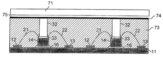
탈착은 주로 TIM 및 리드간에 발생한다. TIM은 실리콘 침니에 양호하게 부착되지만, 리드에는 덜 단단하게 부착된다. 도7은 리드(71) 및 TIM(74) 간에 전개하는 공간(75)을 도시한다.
벤딩 모멘트(bending moment) 및 차동 이평면(differential out of plane) 스트레인들에 의해 생성된 스트레인은 리드 결함 및/또는 IC 디바이스에 대한 침니 결함을 발생시킨다. 이는 도8에 도시된다: 리드 결함의 경우에, 도면 좌측의 실리콘 침니(84)는 도면 우편의 실리콘 침니(85)에 대해 올라간다(raised). 이러한 불일치는 침니 확장 또는 패키지의 다른 엘리먼트의 차이로 인한 결과이다. 이평면 스트레인은 리드(81)를 봉합체(83)로부터 완전히 탈착하거나 부분적으로 탈착시키기에 충분할 수 있다(TIM은 간소화를 위해서 도면에서 생략된다). 도8에 도시되는 바와 같은 이평면 스트레인은 또한 실리콘 침니 상에 벤딩 모멘트를 야기할 수 있다. 직관적으로, 리드가 도면 좌측에서 리프트됨에 따라(여기서 리드는 실리콘 침니(84)로부터 탈착될 수 있다), 기울어진다는 것이 인식될 수 있다. 이는 침니(85) 상에 벤딩 모멘트를 부과하고, 33에서 부착 결함을 가져올 수 있는데, 즉, 침니 및 IC 칩 간의 부착 결함이다.
침니 히트싱크 및 리드 간의 더욱 강한 접속을 위한 방법은 이러한 엘리먼트들 간의 접착성 본드의 무결성을 증가시키는 것으로 여겨질 것이다. 그러나 더 효율적인 방법이 정반대라는 것이 발견되었다. 이러한 엘리먼트 간의 견고한 부착은 리드 결함 문제에 대해 적어도 부분적으로 책임이 있다고 밝혀졌다. 따라서, 리드의 부착을 돕는 기계적 특성들을 가진 오버몰드가 제공되는 새로운 패키지 구조가 디자인된다. 상기 리드는 기계적 특성들을 보상하기 위해 제공된다. 도 1 내지 도 4에 도시된 패키지 디자인에서, 부착물의 접착이 실패하면 패키지에서 리드를 억제할 수 있는 기계적 엘리먼트들이 없다는 것이 이해된다. 기계적 리드 억제부들이 이하 설명되는 디자인들의 특성이다.
도 9는 리드의 단부를 따라 형성된 래빗(rabbet; 94)을 도시한다. 오버몰드(93)은 리드(91)을 억제하기 위해 래빗(92)을 압박하는 기계적 억제 특성(mechanical hold-down features; 94)를 갖는다. 이러한 구조를 형성하기 위해 오버몰드(93)를 적용하기 앞서 침니에 리드를 부착하는 것이 유용하다. 그러나, 상기 부착은 오버몰드(93)이 형성될 때까지 일시적인 부착으로서만 필요하다. 침니들과 리드 사이에 적용되는 양호한 부착 물질들은 상대적으로 소프트한 도전 폴리머들이다. 히트싱크와 리드 사이의 도전 폴리머가 접착성 폴리머 또는 상대적으로 약한 접착성 폴리머가 아닌 것이 또한 바람직하다. 따라서, 실리콘 수지들이 전형적인 에폭시들 위에 있는 것이 바람직하다. 이러한 적용에 적당한 물질은 Lord Thermoset으로부터 입수가능한 Gelease MG 121이다.
원한다면, 종래의 TIM이 여기 설명된 리드 억제부(lid hold-downs)에 부가하여 리드를 본딩하기 위해 사용될 수 있다. 이 경우 TIM이 침니에만 적용되고 도 4에 도시된 바와 같은 오버몰드에는 적용되지 않는다. 실제로 단계 시퀀스는 TIM을 오버몰드에 직접 적용하는 것을 방지하는 것을 단지 도시한다. 리드와 오버몰드 사이의 인터페이스에 TIM이 바람직하다면 리드를 침니들에 부착하기 전에 리드 표면에 적용될 수 있다.
디자인을 위해 리드, 몰드 화합물, 실리콘 침니, IC 디바이스, 침니 다이 부착, IC 다이 부착 및 기판 재료의 열 기계적 특성을 수용하도록 가공되어야하고, TIM은 리드와 침니의 물리적 접촉을 통해 침니와 리드사이의 높은 열 결합 인터페이스를 확실히 하는데 필요하지는 않다는 것을 이해해야 한다. 그러나, 조립동안의 프로세스 제어는 디자인에 TIM 물질을 포함하는 것보다 이러한 디자인을 덜 견고하게 한다.
몰딩 단계동안 리드 억제 특성(94)이 형성되기 때문에 그것들은 오버몰드의 나머지의 부분이 되고 통합된다. 리드 억제부는 여러 형태로 디자인되고 여기에는 일부만 도시된다. 리드(101)의 재진입 측벽(102) 주변의 오버몰드(103)의 몰딩 결과로서 리드 억제 특성(105)이 형성되는 리드 억제의 부가적인 형태가 도 10에 도시된다. 오버몰드의 억제 특성들은 리드의 억제 특성(102)에 보완적인 형상이다.
도 9 및 도 10에 도시된 실시예에서 리드 억제부들은 리드의 단부를 따라 형성된다. 그러나, 상술된 기계적 응력으로 인한 변형이 리드의 중심부에서 일어날 수 있다. 이는 리드의 중간에서 탈착 문제를 일으킨다. 더 큰 억제력을 부가하기 위해 리드 억제부는 전체 리드 영역을 가로지르는 위치에 형성될 수 있다. 이들은 영역 정렬 리드 억제부로 설명될 것이다.
영역 정렬 억제부의 일 예가 도 11에 도시된다. 홈(112)들이 리드(11)에 형성된다. 봉합체(123)이 적용되면, 홈(112)들을 채우고 리드와 오버몰드 사이에 접촉하는 표면적을 증가시킨다. 본 명세서의 다른 도면과 마찬가지로 이 도면도 실제 크기로 도시되지 않았다는 것을 이해해야 한다. 특성들은 명확성을 나타내기 위한 사이즈를 갖는다. 실제 사용되는 특성들은 크거나 작을 수 있다.
도 12에 도시된 홈들은 V 형상이다. 형상들의 폭 넓은 변형이 선택될 수 있다. 예를 들어, 홈들은 데이도 형상(dado shape), 재진입 측벽을 가진 V-홈, T 형, W 형 등 일 수 있다.
영역 정렬 리드 억제부의 4개의 부가적인 예가 도 12 및 13에 도시된다. 두 도면은 두 개의 별개의 실시예에서 침니형 히트싱크를 갖는 디바이스들을 도시한다. 그들은 편의성을 위해 그룹화될 수 있지만, 124, 125, 134, 135에서 4개의 서로 다른 리드 억제 특성들이 도시되는 4개의 서로 다른 디바이스 구조를 나타낸다. 124에 도시된 억제부는 리드(121)을 통해 형성된 구멍(홀)들이다. 이들은 데이도 조인트(dado joint)와 유사한 방식으로 기능한다. 도 12의 125에 도시된 억제는 도브테일 조인트(dovetail joint)와 유사한 방식으로 기능한다. 도 13의 134, 135에 도시된 억제는 리벳(rivet)을 닮는다. 오버몰드 상에 패키지 리드를 유지하는 힘을 효율적으로 제공하는 억제부들을 갖는 이러한 모든 구조들이 명백하다. 영역 정렬 억제부들로 도시된 억제 구성들이 예를 들어, 도 9 및 도 10과 관련하여 상술된 리드의 단부를 따르는 단부 억제부들로서 사용될 수 있다는 것이 명백하다.
상술된 바와 같이, 본 발명의 개념을 따르는 구조의 광범위한 변형들이 디자인될 수 있다. 이들 개념들 중 하나는 오버몰드 바디(overmold body)에서 리드 억제부의 설비이다. 용어 억제(hold-down)가 상기에 자세히 설명되고 몇몇 실시예들이 그 의미를 규정하는 것을 돕기 위해 도시되었다. 패키지의 리드의 하나 이상의 구조적 형상들과 조합하는 몰드 바디에 형성된 임의의 형상 및 몰드 바디와의 통합을 나타내고 패키지 상의 리드를 유지하기 위한 힘을 가한다. 따라서, 본 기술 분야에 이전에 확립된 용어는 아니지만 본 발명을 설명하는데 이 용어를 사용하는 것이 명확하고 적절하다.
언급된 바와 같이 리드 억제부는 리드 및 오버몰드에서 억제 구조를 포함한 다. 리드 및 오버몰드 각각에서 이들 억제 구조들의 형상은 실질적으로 상호보완적이다. 즉, 리드에서 억제 특성의 형상은 오버몰드 바디에서 억제 특성의 형상에 보완적이다.
상술된 바와 같이, 본 발명은 각각의 패키지가 N 개의 IC 디바이스들(여기서 N은 적어도 2)을 포함하는 것을 의미하도록 의도되고, 각각의 IC 디바이스가 히트싱크를 갖는 MCM 패키지에서 주로 사용 가능하다.
본 발명의 다양한 부가적인 변경이 당업자에 의해 행해질 것이다. 기본적으로 종래 기술이 전개되어온 원리 및 그의 등가물에 따른 본 명세서의 특정한 개념들로부터의 모든 변화들이 설명되고 청구되는 바와 같은 본 발명의 범위에 적합하게 고려된다.
도1 내지 도4는 침니-형 히트싱크를 갖는 오버몰딩된 IC 디바이스 패키지를 제조하는 전형적인 단계 시퀀스에 대한 개략도.
도5 및 도6은 이들 디바이스들에서의 결함 모드에 대한 출원인의 인식을 설명하기 위해서 명세서에 사용되는 네 개의 IC 칩들 및 네 개의 침니들의 MCM 패키지의 평면도.
도7 및 도8은 리드가 침니로부터 분리되거나, 침니 및 IC 칩들 간의 본딩의 결함을 초래하는 탈착 모드를 나타내는 MCM 패키지의 측면도.
도9 및 도10은 리드의 단부에서 기계적 특성들이 리드를 패키지에 부착하는 것을 돕도록 사용되는 개선된 패키지 디자인을 도시하는 도면.
도 11 내지 도13은 기계적 특성들이 리드의 영역 상에 확장하는 개선된 패키지 디자인을 도시하는 유사 도면.
Claims (18)
- 오버몰딩된 MCM IC 패키지에 있어서:기판;상기 기판에 부착된 적어도 두 개의 반도체 IC 디바이스들;적어도 두 개의 히트싱크들로서, 각각 IC 디바이스에 부착되고, 상단부 및 하단부를 가지며, 상기 하단부는 IC 디바이스에 부착되는, 상기 히트싱크들;반도체 디바이스들 및 히트싱크들을 캡슐화하는 폴리머 오버몰드로서, 상기 오버몰드는 상기 히트싱크들의 상단부들이 노출된 상단부표면을 형성하고, 상기 상단부표면에 복수의 리드 억제부(lid hold-downs)들을 갖는, 폴리머 오버몰드; 및상기 오버몰드에 부착된 리드로서, 상기 리드는 복수의 리드 억제부들을 갖고, 상기 오버몰드의 리드 억제부들은 상기 리드의 리드 억제부들을 인게이지하는, 상기 오버몰드에 부착된 리드를 포함하는, 오버몰딩된 MCM IC 패키지.
- 제 1항에 있어서, 상기 오버몰드 및 상기 리드의 리드 억제부들은 각각 형상을 갖고, 상기 오버몰드의 억제부들의 형상은 상기 리드의 리드 억제부들의 형상과 보완적 쌍(complement)을 이루는, 오버몰딩된 MCM IC 패키지.
- 제 2항에 있어서, 상기 IC 디바이스들은 와이어 본드들로 상기 기판에 전기적으로 접속되는, 오버몰딩된 MCM IC 패키지.
- 제 2항에 있어서, 상기 히트싱크와 상기 리드 사이에 제 1 도전성 폴리머가 선택적으로 위치되는, 오버몰딩된 MCM IC 패키지.
- 제 4항에 있어서, 상기 오버몰드와 상기 리드 사이에 제 2 도전성 폴리머가 선택적으로 위치되고, 상기 제 1 도전성 폴리머와 상기 제 2 도전성 폴리머는 서로 다른, 오버몰딩된 MCM IC 패키지.
- 제 4항에 있어서, 상기 제 1 도전성 폴리머는 접착성 폴리머가 아닌, 오버몰딩된 MCM IC 패키지.
- 제 2항에 있어서, 상기 히트싱크는 실리콘인, 오버몰딩된 MCM IC 패키지.
- 제 2항에 있어서, 상기 리드는 구리인, 오버몰딩된 MCM IC 패키지.
- 제 2항에 있어서, 적어도 4개의 IC 디바이스들을 갖는, 오버몰딩된 MCM IC 패키지.
- 오버몰딩된 MCM IC 패키지의 제조 방법에 있어서,N 개의 반도체 IC 디바이스들을 기판에 부착하는 단계로서, 상기 N은 적어도 2인, 반도체 IC 디바이스 부착 단계,상기 IC 디바이스들에 N 개의 히트싱크들을 부착하는 단계로서, 각각의 IC 디바이스는 히트싱크를 가지며, 상기 히트싱크는 IC 디바이스에 부착된 하단부와, 상단부를 갖는, 히트싱크 부착 단계,상기 히트싱크의 상단부에 리드를 부착하는 단계로서, 상기 리드는 복수의 리드 억제부들을 갖는, 리드 부착 단계,상기 IC 디바이스들과 상기 히트싱크들을 캡슐화하는 오버몰드를 몰딩하는 단계로서, 상기 오버몰드 몰딩 단계는 상기 오버몰드와 통합된 복수의 리드 억제부들을 형성하는 단계를 포함하고, 상기 오버몰드내의 상기 리드 억제부는 상기 리드의 상기 리드 억제부를 채우는, 오버몰딩된 MCM IC 패키지의 제조 방법.
- 제 10항에 있어서, 상기 오버몰드 및 상기 리드의 리드 억제부들은 각각 형상을 갖고, 상기 오버몰드의 억제부들의 형상은 상기 리드의 리드 억제부들의 형상과 보완적 쌍을 이루는, 오버몰딩된 MCM IC 패키지의 제조 방법.
- 제 11항에 있어서, 상기 IC 디바이스들은 와이어 본드들로 상기 기판에 전기적으로 접속되는, 오버몰딩된 MCM IC 패키지의 제조 방법.
- 제 11항에 있어서, 상기 리드는 제 1 도전성 폴리머를 이용하여 상기 히트싱크들에 부착되는, 오버몰딩된 MCM IC 패키지의 제조 방법.
- 제 13항에 있어서, 제 2 도전성 폴리머가 상기 리드를 상기 히트싱크들에 부착하기 전에 상기 리드에 적용되고 상기 제 1 도전성 폴리머는 상기 제 2 도전성 폴리머와 서로 다른, 오버몰딩된 MCM IC 패키지의 제조 방법.
- 제 13항에 있어서, 상기 제 1 도전성 폴리머는 접착성 폴리머가 아닌, 오버몰딩된 MCM IC 패키지의 제조 방법.
- 제 11항에 있어서, 상기 히트싱크는 실리콘인, 오버몰딩된 MCM IC 패키지의 제조 방법.
- 제 11항에 있어서, 상기 리드는 구리인, 오버몰딩된 MCM IC 패키지의 제조 방법.
- 제 11항에 있어서, N은 적어도 4인, 오버몰딩된 MCM IC 패키지의 제조 방법.
Applications Claiming Priority (2)
| Application Number | Priority Date | Filing Date | Title |
|---|---|---|---|
| US11/504,989 | 2006-08-16 | ||
| US11/504,989 US20080042302A1 (en) | 2006-08-16 | 2006-08-16 | Plastic overmolded packages with molded lid attachments |
Publications (1)
| Publication Number | Publication Date |
|---|---|
| KR20080015724A true KR20080015724A (ko) | 2008-02-20 |
Family
ID=39095324
Family Applications (1)
| Application Number | Title | Priority Date | Filing Date |
|---|---|---|---|
| KR1020070079026A KR20080015724A (ko) | 2006-08-16 | 2007-08-07 | 몰딩된 리드 부착물을 갖는 플라스틱 오버몰딩된 패키지들 |
Country Status (4)
| Country | Link |
|---|---|
| US (1) | US20080042302A1 (ko) |
| JP (1) | JP5121354B2 (ko) |
| KR (1) | KR20080015724A (ko) |
| CN (1) | CN101127348B (ko) |
Families Citing this family (8)
| Publication number | Priority date | Publication date | Assignee | Title |
|---|---|---|---|---|
| US8049313B2 (en) * | 2006-09-20 | 2011-11-01 | Freescale Semiconductor, Inc. | Heat spreader for semiconductor package |
| JP2008305937A (ja) * | 2007-06-07 | 2008-12-18 | Panasonic Corp | 電子部品内蔵モジュールおよびその製造方法 |
| US8801463B2 (en) | 2012-01-13 | 2014-08-12 | Hon Hai Precision Industry Co., Ltd. | Waterproof electrical connector |
| US9093563B2 (en) | 2013-07-11 | 2015-07-28 | International Business Machines Corporation | Electronic module assembly with patterned adhesive array |
| US9337119B2 (en) | 2014-07-14 | 2016-05-10 | Micron Technology, Inc. | Stacked semiconductor die assemblies with high efficiency thermal paths and associated systems |
| JP6897056B2 (ja) * | 2016-10-20 | 2021-06-30 | 富士電機株式会社 | 半導体装置及び半導体装置製造方法 |
| KR102617088B1 (ko) | 2019-09-18 | 2023-12-26 | 삼성전자주식회사 | 반도체 패키지 |
| JP7247124B2 (ja) * | 2020-01-07 | 2023-03-28 | 三菱電機株式会社 | 半導体モジュール |
Family Cites Families (14)
| Publication number | Priority date | Publication date | Assignee | Title |
|---|---|---|---|---|
| JPH0758254A (ja) * | 1993-08-19 | 1995-03-03 | Fujitsu Ltd | マルチチップモジュール及びその製造方法 |
| JPH10242355A (ja) * | 1997-02-25 | 1998-09-11 | Hitachi Ltd | 半導体集積回路装置 |
| US6507116B1 (en) * | 1997-04-24 | 2003-01-14 | International Business Machines Corporation | Electronic package and method of forming |
| TW411595B (en) * | 1999-03-20 | 2000-11-11 | Siliconware Precision Industries Co Ltd | Heat structure for semiconductor package device |
| US6784541B2 (en) * | 2000-01-27 | 2004-08-31 | Hitachi, Ltd. | Semiconductor module and mounting method for same |
| TW454321B (en) * | 2000-09-13 | 2001-09-11 | Siliconware Precision Industries Co Ltd | Semiconductor package with heat dissipation structure |
| US6849940B1 (en) * | 2000-11-20 | 2005-02-01 | Ati Technologies, Inc. | Integrated circuit package for the transfer of heat generated by the inte circuit and method of fabricating same |
| JP4479121B2 (ja) * | 2001-04-25 | 2010-06-09 | 株式会社デンソー | 半導体装置の製造方法 |
| JP3640625B2 (ja) * | 2001-07-02 | 2005-04-20 | 新光電気工業株式会社 | 半導体装置と半導体装置用フイルムキャリア |
| US6734552B2 (en) * | 2001-07-11 | 2004-05-11 | Asat Limited | Enhanced thermal dissipation integrated circuit package |
| US6987032B1 (en) * | 2002-07-19 | 2006-01-17 | Asat Ltd. | Ball grid array package and process for manufacturing same |
| US6979594B1 (en) * | 2002-07-19 | 2005-12-27 | Asat Ltd. | Process for manufacturing ball grid array package |
| US6800948B1 (en) * | 2002-07-19 | 2004-10-05 | Asat Ltd. | Ball grid array package |
| KR100632459B1 (ko) * | 2004-01-28 | 2006-10-09 | 삼성전자주식회사 | 열방출형 반도체 패키지 및 그 제조방법 |
-
2006
- 2006-08-16 US US11/504,989 patent/US20080042302A1/en not_active Abandoned
-
2007
- 2007-06-21 CN CN2007101120354A patent/CN101127348B/zh not_active Expired - Fee Related
- 2007-08-07 KR KR1020070079026A patent/KR20080015724A/ko active IP Right Grant
- 2007-08-16 JP JP2007212211A patent/JP5121354B2/ja not_active Expired - Fee Related
Also Published As
| Publication number | Publication date |
|---|---|
| JP2008047920A (ja) | 2008-02-28 |
| CN101127348B (zh) | 2011-07-13 |
| US20080042302A1 (en) | 2008-02-21 |
| CN101127348A (zh) | 2008-02-20 |
| JP5121354B2 (ja) | 2013-01-16 |
Similar Documents
| Publication | Publication Date | Title |
|---|---|---|
| JP5121353B2 (ja) | オーバーモールドされたmcmicパッケージ及びその製造方法 | |
| US7186585B2 (en) | Method of manufacturing an integrated heat spreader lid | |
| US7279789B2 (en) | Thermally enhanced three-dimensional package and method for manufacturing the same | |
| KR101173924B1 (ko) | 반도체 장치 | |
| US6849942B2 (en) | Semiconductor package with heat sink attached to substrate | |
| KR20080015724A (ko) | 몰딩된 리드 부착물을 갖는 플라스틱 오버몰딩된 패키지들 | |
| JP4454181B2 (ja) | 半導体装置 | |
| US20030045029A1 (en) | Semiconductor device and method for manufacturing the same | |
| JPH07169882A (ja) | モールドされた集積回路パッケージ | |
| KR20050077866A (ko) | 열방출형 반도체 패키지 및 그 제조방법 | |
| US7605020B2 (en) | Semiconductor chip package | |
| US20060038202A1 (en) | Heatsink apparatus and thermally-conductive intermediate material for dissipating heat in semiconductor packages | |
| US20190141834A1 (en) | Mechanically-compliant and electrically and thermally conductive leadframes for component-on-package circuits | |
| JP2007281201A (ja) | 半導体装置 | |
| JP4626445B2 (ja) | 半導体パッケージの製造方法 | |
| CN113113391A (zh) | 用于双面功率模块的引线框间隔件 | |
| US20210111093A1 (en) | Heterogeneous Lid Seal Band for Structural Stability in Multiple Integrated Circuit (IC) Device Modules | |
| US6784536B1 (en) | Symmetric stack up structure for organic BGA chip carriers | |
| US20020145207A1 (en) | Method and structure for integrated circuit package | |
| US20220148955A1 (en) | Semiconductor package | |
| US8482019B2 (en) | Electronic light emitting device and method for fabricating the same | |
| JPH0831986A (ja) | 放熱板付半導体装置 | |
| KR20050022650A (ko) | 리드 프레임을 이용한 비지에이 패키지 | |
| KR20130134031A (ko) | Pop 패키지 및 그 제조방법 | |
| KR20020065273A (ko) | 반도체 패키지 및 반도체 패키지의 마더보드 실장방법 |
Legal Events
| Date | Code | Title | Description |
|---|---|---|---|
| A201 | Request for examination | ||
| E902 | Notification of reason for refusal | ||
| E701 | Decision to grant or registration of patent right |