KR101436791B1 - Composite material, light-emitting element, light-emitting device, and manufacturing method thereof - Google Patents
Composite material, light-emitting element, light-emitting device, and manufacturing method thereof Download PDFInfo
- Publication number
- KR101436791B1 KR101436791B1 KR1020077012150A KR20077012150A KR101436791B1 KR 101436791 B1 KR101436791 B1 KR 101436791B1 KR 1020077012150 A KR1020077012150 A KR 1020077012150A KR 20077012150 A KR20077012150 A KR 20077012150A KR 101436791 B1 KR101436791 B1 KR 101436791B1
- Authority
- KR
- South Korea
- Prior art keywords
- composite material
- metal
- light emitting
- delete delete
- metal oxide
- Prior art date
Links
- 239000002131 composite material Substances 0.000 title claims abstract description 207
- 238000004519 manufacturing process Methods 0.000 title abstract description 18
- 229910052751 metal Inorganic materials 0.000 claims abstract description 172
- 239000002184 metal Substances 0.000 claims abstract description 172
- 150000004706 metal oxides Chemical group 0.000 claims abstract description 165
- 150000002894 organic compounds Chemical group 0.000 claims abstract description 158
- 229910044991 metal oxide Inorganic materials 0.000 claims abstract description 123
- 239000013522 chelant Substances 0.000 claims abstract description 41
- VYPSYNLAJGMNEJ-UHFFFAOYSA-N Silicium dioxide Chemical compound O=[Si]=O VYPSYNLAJGMNEJ-UHFFFAOYSA-N 0.000 claims description 25
- 229910052814 silicon oxide Inorganic materials 0.000 claims description 21
- 229910052782 aluminium Inorganic materials 0.000 claims description 19
- XAGFODPZIPBFFR-UHFFFAOYSA-N aluminium Chemical compound [Al] XAGFODPZIPBFFR-UHFFFAOYSA-N 0.000 claims description 18
- ZOKXTWBITQBERF-UHFFFAOYSA-N Molybdenum Chemical compound [Mo] ZOKXTWBITQBERF-UHFFFAOYSA-N 0.000 claims description 15
- 229910052750 molybdenum Inorganic materials 0.000 claims description 15
- 239000011733 molybdenum Substances 0.000 claims description 13
- 229910052719 titanium Inorganic materials 0.000 claims description 13
- 239000010936 titanium Substances 0.000 claims description 13
- RTAQQCXQSZGOHL-UHFFFAOYSA-N Titanium Chemical compound [Ti] RTAQQCXQSZGOHL-UHFFFAOYSA-N 0.000 claims description 12
- WFKWXMTUELFFGS-UHFFFAOYSA-N tungsten Chemical compound [W] WFKWXMTUELFFGS-UHFFFAOYSA-N 0.000 claims description 9
- 229910052721 tungsten Inorganic materials 0.000 claims description 9
- 239000010937 tungsten Substances 0.000 claims description 9
- 229910052720 vanadium Inorganic materials 0.000 claims description 8
- LEONUFNNVUYDNQ-UHFFFAOYSA-N vanadium atom Chemical compound [V] LEONUFNNVUYDNQ-UHFFFAOYSA-N 0.000 claims description 8
- UGUHFDPGDQDVGX-UHFFFAOYSA-N 1,2,3-thiadiazole Chemical group C1=CSN=N1 UGUHFDPGDQDVGX-UHFFFAOYSA-N 0.000 claims description 7
- JUJWROOIHBZHMG-UHFFFAOYSA-N Pyridine Chemical group C1=CC=NC=C1 JUJWROOIHBZHMG-UHFFFAOYSA-N 0.000 claims description 7
- 229910052783 alkali metal Inorganic materials 0.000 claims description 7
- 150000001340 alkali metals Chemical class 0.000 claims description 7
- 125000005264 aryl amine group Chemical group 0.000 claims description 7
- 229910052791 calcium Inorganic materials 0.000 claims description 7
- 239000011575 calcium Substances 0.000 claims description 7
- 229910052758 niobium Inorganic materials 0.000 claims description 7
- 239000010955 niobium Substances 0.000 claims description 7
- GUCVJGMIXFAOAE-UHFFFAOYSA-N niobium atom Chemical compound [Nb] GUCVJGMIXFAOAE-UHFFFAOYSA-N 0.000 claims description 7
- TWNQGVIAIRXVLR-UHFFFAOYSA-N oxo(oxoalumanyloxy)alumane Chemical compound O=[Al]O[Al]=O TWNQGVIAIRXVLR-UHFFFAOYSA-N 0.000 claims description 7
- OYPRJOBELJOOCE-UHFFFAOYSA-N Calcium Chemical compound [Ca] OYPRJOBELJOOCE-UHFFFAOYSA-N 0.000 claims description 6
- WHXSMMKQMYFTQS-UHFFFAOYSA-N Lithium Chemical compound [Li] WHXSMMKQMYFTQS-UHFFFAOYSA-N 0.000 claims description 6
- KJTLSVCANCCWHF-UHFFFAOYSA-N Ruthenium Chemical compound [Ru] KJTLSVCANCCWHF-UHFFFAOYSA-N 0.000 claims description 6
- FZWLAAWBMGSTSO-UHFFFAOYSA-N Thiazole Chemical group C1=CSC=N1 FZWLAAWBMGSTSO-UHFFFAOYSA-N 0.000 claims description 6
- 229910052784 alkaline earth metal Inorganic materials 0.000 claims description 6
- 150000001342 alkaline earth metals Chemical class 0.000 claims description 6
- 229910052788 barium Inorganic materials 0.000 claims description 6
- DSAJWYNOEDNPEQ-UHFFFAOYSA-N barium atom Chemical compound [Ba] DSAJWYNOEDNPEQ-UHFFFAOYSA-N 0.000 claims description 6
- 125000002883 imidazolyl group Chemical group 0.000 claims description 6
- 229910052744 lithium Inorganic materials 0.000 claims description 6
- 125000002971 oxazolyl group Chemical group 0.000 claims description 6
- 125000003373 pyrazinyl group Chemical group 0.000 claims description 6
- 229910052702 rhenium Inorganic materials 0.000 claims description 6
- WUAPFZMCVAUBPE-UHFFFAOYSA-N rhenium atom Chemical compound [Re] WUAPFZMCVAUBPE-UHFFFAOYSA-N 0.000 claims description 6
- 229910052707 ruthenium Inorganic materials 0.000 claims description 6
- 229910052723 transition metal Inorganic materials 0.000 claims description 6
- 150000003624 transition metals Chemical class 0.000 claims description 6
- JYEUMXHLPRZUAT-UHFFFAOYSA-N 1,2,3-triazine Chemical group C1=CN=NN=C1 JYEUMXHLPRZUAT-UHFFFAOYSA-N 0.000 claims description 5
- GYHNNYVSQQEPJS-UHFFFAOYSA-N Gallium Chemical compound [Ga] GYHNNYVSQQEPJS-UHFFFAOYSA-N 0.000 claims description 5
- 229910052733 gallium Inorganic materials 0.000 claims description 5
- 229910052738 indium Inorganic materials 0.000 claims description 5
- APFVFJFRJDLVQX-UHFFFAOYSA-N indium atom Chemical compound [In] APFVFJFRJDLVQX-UHFFFAOYSA-N 0.000 claims description 5
- WCPAKWJPBJAGKN-UHFFFAOYSA-N oxadiazole Chemical group C1=CON=N1 WCPAKWJPBJAGKN-UHFFFAOYSA-N 0.000 claims description 5
- 125000001425 triazolyl group Chemical group 0.000 claims description 5
- 239000010410 layer Substances 0.000 description 232
- 239000010408 film Substances 0.000 description 67
- 239000000758 substrate Substances 0.000 description 55
- 150000004703 alkoxides Chemical class 0.000 description 54
- 239000003381 stabilizer Substances 0.000 description 53
- 239000000463 material Substances 0.000 description 49
- 238000002347 injection Methods 0.000 description 42
- 239000007924 injection Substances 0.000 description 42
- 238000000034 method Methods 0.000 description 40
- 239000003446 ligand Substances 0.000 description 34
- 239000004065 semiconductor Substances 0.000 description 31
- 238000006243 chemical reaction Methods 0.000 description 28
- IJGRMHOSHXDMSA-UHFFFAOYSA-N Atomic nitrogen Chemical compound N#N IJGRMHOSHXDMSA-UHFFFAOYSA-N 0.000 description 22
- 239000010409 thin film Substances 0.000 description 22
- 238000010304 firing Methods 0.000 description 21
- 239000011229 interlayer Substances 0.000 description 18
- XLYOFNOQVPJJNP-UHFFFAOYSA-N water Substances O XLYOFNOQVPJJNP-UHFFFAOYSA-N 0.000 description 16
- 238000010586 diagram Methods 0.000 description 15
- 230000007062 hydrolysis Effects 0.000 description 14
- 238000006460 hydrolysis reaction Methods 0.000 description 14
- 238000000576 coating method Methods 0.000 description 13
- 239000000243 solution Substances 0.000 description 13
- XKRFYHLGVUSROY-UHFFFAOYSA-N Argon Chemical compound [Ar] XKRFYHLGVUSROY-UHFFFAOYSA-N 0.000 description 12
- 239000002585 base Substances 0.000 description 12
- 239000000428 dust Substances 0.000 description 12
- 239000002346 layers by function Substances 0.000 description 12
- 239000011159 matrix material Substances 0.000 description 12
- 150000002739 metals Chemical class 0.000 description 12
- 239000003960 organic solvent Substances 0.000 description 12
- PQQKPALAQIIWST-UHFFFAOYSA-N oxomolybdenum Chemical compound [Mo]=O PQQKPALAQIIWST-UHFFFAOYSA-N 0.000 description 12
- XYIBRDXRRQCHLP-UHFFFAOYSA-N ethyl acetoacetate Chemical compound CCOC(=O)CC(C)=O XYIBRDXRRQCHLP-UHFFFAOYSA-N 0.000 description 11
- 229940093858 ethyl acetoacetate Drugs 0.000 description 11
- 229910052757 nitrogen Inorganic materials 0.000 description 11
- KDZOCMHDOCFKRK-UHFFFAOYSA-N 5-(n-phenylanilino)quinolin-8-ol Chemical compound C12=CC=CN=C2C(O)=CC=C1N(C=1C=CC=CC=1)C1=CC=CC=C1 KDZOCMHDOCFKRK-UHFFFAOYSA-N 0.000 description 10
- WYURNTSHIVDZCO-UHFFFAOYSA-N Tetrahydrofuran Chemical compound C1CCOC1 WYURNTSHIVDZCO-UHFFFAOYSA-N 0.000 description 10
- 229910000476 molybdenum oxide Inorganic materials 0.000 description 10
- WEVYAHXRMPXWCK-UHFFFAOYSA-N Acetonitrile Chemical compound CC#N WEVYAHXRMPXWCK-UHFFFAOYSA-N 0.000 description 9
- YMWUJEATGCHHMB-UHFFFAOYSA-N Dichloromethane Chemical compound ClCCl YMWUJEATGCHHMB-UHFFFAOYSA-N 0.000 description 9
- LFQSCWFLJHTTHZ-UHFFFAOYSA-N Ethanol Chemical compound CCO LFQSCWFLJHTTHZ-UHFFFAOYSA-N 0.000 description 9
- OKKJLVBELUTLKV-UHFFFAOYSA-N Methanol Chemical compound OC OKKJLVBELUTLKV-UHFFFAOYSA-N 0.000 description 9
- 230000007547 defect Effects 0.000 description 9
- 230000000694 effects Effects 0.000 description 9
- 230000002378 acidificating effect Effects 0.000 description 8
- 239000003990 capacitor Substances 0.000 description 8
- 238000010438 heat treatment Methods 0.000 description 8
- 239000012535 impurity Substances 0.000 description 8
- 229920005989 resin Polymers 0.000 description 8
- 239000011347 resin Substances 0.000 description 8
- 239000003566 sealing material Substances 0.000 description 8
- 229910052581 Si3N4 Inorganic materials 0.000 description 7
- XUIMIQQOPSSXEZ-UHFFFAOYSA-N Silicon Chemical compound [Si] XUIMIQQOPSSXEZ-UHFFFAOYSA-N 0.000 description 7
- 150000001875 compounds Chemical class 0.000 description 7
- 229910052710 silicon Inorganic materials 0.000 description 7
- 239000010703 silicon Substances 0.000 description 7
- HQVNEWCFYHHQES-UHFFFAOYSA-N silicon nitride Chemical compound N12[Si]34N5[Si]62N3[Si]51N64 HQVNEWCFYHHQES-UHFFFAOYSA-N 0.000 description 7
- PXHVJJICTQNCMI-UHFFFAOYSA-N Nickel Chemical compound [Ni] PXHVJJICTQNCMI-UHFFFAOYSA-N 0.000 description 6
- XHCLAFWTIXFWPH-UHFFFAOYSA-N [O-2].[O-2].[O-2].[O-2].[O-2].[V+5].[V+5] Chemical group [O-2].[O-2].[O-2].[O-2].[O-2].[V+5].[V+5] XHCLAFWTIXFWPH-UHFFFAOYSA-N 0.000 description 6
- 238000000862 absorption spectrum Methods 0.000 description 6
- YRKCREAYFQTBPV-UHFFFAOYSA-N acetylacetone Chemical compound CC(=O)CC(C)=O YRKCREAYFQTBPV-UHFFFAOYSA-N 0.000 description 6
- 229910021417 amorphous silicon Inorganic materials 0.000 description 6
- 229910052786 argon Inorganic materials 0.000 description 6
- 230000004888 barrier function Effects 0.000 description 6
- 238000005530 etching Methods 0.000 description 6
- 239000007789 gas Substances 0.000 description 6
- 239000011261 inert gas Substances 0.000 description 6
- 238000001556 precipitation Methods 0.000 description 6
- BDERNNFJNOPAEC-UHFFFAOYSA-N propan-1-ol Chemical compound CCCO BDERNNFJNOPAEC-UHFFFAOYSA-N 0.000 description 6
- 239000002356 single layer Substances 0.000 description 6
- 239000004642 Polyimide Substances 0.000 description 5
- 238000010521 absorption reaction Methods 0.000 description 5
- NIXOWILDQLNWCW-UHFFFAOYSA-N acrylic acid group Chemical group C(C=C)(=O)O NIXOWILDQLNWCW-UHFFFAOYSA-N 0.000 description 5
- 239000011248 coating agent Substances 0.000 description 5
- 230000000052 comparative effect Effects 0.000 description 5
- 239000011368 organic material Substances 0.000 description 5
- 229960003540 oxyquinoline Drugs 0.000 description 5
- 229920001721 polyimide Polymers 0.000 description 5
- 238000003980 solgel method Methods 0.000 description 5
- 239000000126 substance Substances 0.000 description 5
- YLQBMQCUIZJEEH-UHFFFAOYSA-N tetrahydrofuran Natural products C=1C=COC=1 YLQBMQCUIZJEEH-UHFFFAOYSA-N 0.000 description 5
- -1 5- Quinolinol (diphenylamino-8-quinolinol) Chemical compound 0.000 description 4
- OKTJSMMVPCPJKN-UHFFFAOYSA-N Carbon Chemical compound [C] OKTJSMMVPCPJKN-UHFFFAOYSA-N 0.000 description 4
- LRHPLDYGYMQRHN-UHFFFAOYSA-N N-Butanol Chemical compound CCCCO LRHPLDYGYMQRHN-UHFFFAOYSA-N 0.000 description 4
- 230000015572 biosynthetic process Effects 0.000 description 4
- BRPQOXSCLDDYGP-UHFFFAOYSA-N calcium oxide Chemical compound [O-2].[Ca+2] BRPQOXSCLDDYGP-UHFFFAOYSA-N 0.000 description 4
- ODINCKMPIJJUCX-UHFFFAOYSA-N calcium oxide Inorganic materials [Ca]=O ODINCKMPIJJUCX-UHFFFAOYSA-N 0.000 description 4
- 239000000292 calcium oxide Substances 0.000 description 4
- 229910052799 carbon Inorganic materials 0.000 description 4
- 229910052802 copper Inorganic materials 0.000 description 4
- 239000010949 copper Substances 0.000 description 4
- 239000013078 crystal Substances 0.000 description 4
- 238000002425 crystallisation Methods 0.000 description 4
- 230000008025 crystallization Effects 0.000 description 4
- 230000001747 exhibiting effect Effects 0.000 description 4
- 238000001879 gelation Methods 0.000 description 4
- 230000005525 hole transport Effects 0.000 description 4
- 238000007654 immersion Methods 0.000 description 4
- 238000010030 laminating Methods 0.000 description 4
- 229910001510 metal chloride Inorganic materials 0.000 description 4
- 229910052760 oxygen Inorganic materials 0.000 description 4
- 238000005192 partition Methods 0.000 description 4
- 238000005268 plasma chemical vapour deposition Methods 0.000 description 4
- BASFCYQUMIYNBI-UHFFFAOYSA-N platinum Chemical compound [Pt] BASFCYQUMIYNBI-UHFFFAOYSA-N 0.000 description 4
- 238000002360 preparation method Methods 0.000 description 4
- 239000010453 quartz Substances 0.000 description 4
- MCJGNVYPOGVAJF-UHFFFAOYSA-N quinolin-8-ol Chemical compound C1=CN=C2C(O)=CC=CC2=C1 MCJGNVYPOGVAJF-UHFFFAOYSA-N 0.000 description 4
- 229910021332 silicide Inorganic materials 0.000 description 4
- FVBUAEGBCNSCDD-UHFFFAOYSA-N silicide(4-) Chemical compound [Si-4] FVBUAEGBCNSCDD-UHFFFAOYSA-N 0.000 description 4
- 229910052709 silver Inorganic materials 0.000 description 4
- 238000004528 spin coating Methods 0.000 description 4
- SCYULBFZEHDVBN-UHFFFAOYSA-N 1,1-Dichloroethane Chemical compound CC(Cl)Cl SCYULBFZEHDVBN-UHFFFAOYSA-N 0.000 description 3
- CVBUKMMMRLOKQR-UHFFFAOYSA-N 1-phenylbutane-1,3-dione Chemical compound CC(=O)CC(=O)C1=CC=CC=C1 CVBUKMMMRLOKQR-UHFFFAOYSA-N 0.000 description 3
- HZAXFHJVJLSVMW-UHFFFAOYSA-N 2-Aminoethan-1-ol Chemical compound NCCO HZAXFHJVJLSVMW-UHFFFAOYSA-N 0.000 description 3
- RYGMFSIKBFXOCR-UHFFFAOYSA-N Copper Chemical compound [Cu] RYGMFSIKBFXOCR-UHFFFAOYSA-N 0.000 description 3
- PIICEJLVQHRZGT-UHFFFAOYSA-N Ethylenediamine Chemical compound NCCN PIICEJLVQHRZGT-UHFFFAOYSA-N 0.000 description 3
- UFHFLCQGNIYNRP-UHFFFAOYSA-N Hydrogen Chemical compound [H][H] UFHFLCQGNIYNRP-UHFFFAOYSA-N 0.000 description 3
- XEEYBQQBJWHFJM-UHFFFAOYSA-N Iron Chemical compound [Fe] XEEYBQQBJWHFJM-UHFFFAOYSA-N 0.000 description 3
- KFZMGEQAYNKOFK-UHFFFAOYSA-N Isopropanol Chemical compound CC(C)O KFZMGEQAYNKOFK-UHFFFAOYSA-N 0.000 description 3
- KDLHZDBZIXYQEI-UHFFFAOYSA-N Palladium Chemical compound [Pd] KDLHZDBZIXYQEI-UHFFFAOYSA-N 0.000 description 3
- 150000001298 alcohols Chemical class 0.000 description 3
- 150000001414 amino alcohols Chemical class 0.000 description 3
- QVGXLLKOCUKJST-UHFFFAOYSA-N atomic oxygen Chemical compound [O] QVGXLLKOCUKJST-UHFFFAOYSA-N 0.000 description 3
- 238000001354 calcination Methods 0.000 description 3
- 230000001413 cellular effect Effects 0.000 description 3
- 239000002738 chelating agent Substances 0.000 description 3
- 229910021419 crystalline silicon Inorganic materials 0.000 description 3
- 239000002274 desiccant Substances 0.000 description 3
- 150000004985 diamines Chemical class 0.000 description 3
- KPUWHANPEXNPJT-UHFFFAOYSA-N disiloxane Chemical class [SiH3]O[SiH3] KPUWHANPEXNPJT-UHFFFAOYSA-N 0.000 description 3
- 230000005281 excited state Effects 0.000 description 3
- 239000011521 glass Substances 0.000 description 3
- 239000001257 hydrogen Substances 0.000 description 3
- 229910052739 hydrogen Inorganic materials 0.000 description 3
- 230000001771 impaired effect Effects 0.000 description 3
- 238000005499 laser crystallization Methods 0.000 description 3
- 239000012046 mixed solvent Substances 0.000 description 3
- 238000012986 modification Methods 0.000 description 3
- 230000004048 modification Effects 0.000 description 3
- 239000001301 oxygen Substances 0.000 description 3
- 238000006068 polycondensation reaction Methods 0.000 description 3
- 230000000087 stabilizing effect Effects 0.000 description 3
- 238000012546 transfer Methods 0.000 description 3
- 229910001935 vanadium oxide Inorganic materials 0.000 description 3
- PNEYBMLMFCGWSK-UHFFFAOYSA-N Alumina Chemical group [O-2].[O-2].[O-2].[Al+3].[Al+3] PNEYBMLMFCGWSK-UHFFFAOYSA-N 0.000 description 2
- VHUUQVKOLVNVRT-UHFFFAOYSA-N Ammonium hydroxide Chemical compound [NH4+].[OH-] VHUUQVKOLVNVRT-UHFFFAOYSA-N 0.000 description 2
- VYZAMTAEIAYCRO-UHFFFAOYSA-N Chromium Chemical compound [Cr] VYZAMTAEIAYCRO-UHFFFAOYSA-N 0.000 description 2
- OAICVXFJPJFONN-UHFFFAOYSA-N Phosphorus Chemical compound [P] OAICVXFJPJFONN-UHFFFAOYSA-N 0.000 description 2
- 206010034972 Photosensitivity reaction Diseases 0.000 description 2
- 229910000577 Silicon-germanium Inorganic materials 0.000 description 2
- PPBRXRYQALVLMV-UHFFFAOYSA-N Styrene Chemical compound C=CC1=CC=CC=C1 PPBRXRYQALVLMV-UHFFFAOYSA-N 0.000 description 2
- ATJFFYVFTNAWJD-UHFFFAOYSA-N Tin Chemical compound [Sn] ATJFFYVFTNAWJD-UHFFFAOYSA-N 0.000 description 2
- LEVVHYCKPQWKOP-UHFFFAOYSA-N [Si].[Ge] Chemical compound [Si].[Ge] LEVVHYCKPQWKOP-UHFFFAOYSA-N 0.000 description 2
- HPLXJFZCZSBAAH-UHFFFAOYSA-N [V+3].CC(C)[O-].CC(C)[O-].CC(C)[O-] Chemical compound [V+3].CC(C)[O-].CC(C)[O-].CC(C)[O-] HPLXJFZCZSBAAH-UHFFFAOYSA-N 0.000 description 2
- WDJHALXBUFZDSR-UHFFFAOYSA-M acetoacetate Chemical compound CC(=O)CC([O-])=O WDJHALXBUFZDSR-UHFFFAOYSA-M 0.000 description 2
- 239000002253 acid Substances 0.000 description 2
- 239000000956 alloy Substances 0.000 description 2
- 235000011114 ammonium hydroxide Nutrition 0.000 description 2
- 229910052804 chromium Inorganic materials 0.000 description 2
- 239000011651 chromium Substances 0.000 description 2
- 238000000354 decomposition reaction Methods 0.000 description 2
- 238000009792 diffusion process Methods 0.000 description 2
- 238000001312 dry etching Methods 0.000 description 2
- YZEGBLRYVFVTTE-UHFFFAOYSA-N ethanolate;molybdenum Chemical compound [Mo].CC[O-].CC[O-].CC[O-].CC[O-].CC[O-] YZEGBLRYVFVTTE-UHFFFAOYSA-N 0.000 description 2
- 239000000945 filler Substances 0.000 description 2
- PCHJSUWPFVWCPO-UHFFFAOYSA-N gold Chemical compound [Au] PCHJSUWPFVWCPO-UHFFFAOYSA-N 0.000 description 2
- 229910052737 gold Inorganic materials 0.000 description 2
- 239000010931 gold Substances 0.000 description 2
- 238000005984 hydrogenation reaction Methods 0.000 description 2
- 229910010272 inorganic material Inorganic materials 0.000 description 2
- 239000011147 inorganic material Substances 0.000 description 2
- 238000003780 insertion Methods 0.000 description 2
- 230000037431 insertion Effects 0.000 description 2
- 238000003475 lamination Methods 0.000 description 2
- 229910000000 metal hydroxide Inorganic materials 0.000 description 2
- 150000004692 metal hydroxides Chemical class 0.000 description 2
- PDKHNCYLMVRIFV-UHFFFAOYSA-H molybdenum;hexachloride Chemical compound [Cl-].[Cl-].[Cl-].[Cl-].[Cl-].[Cl-].[Mo] PDKHNCYLMVRIFV-UHFFFAOYSA-H 0.000 description 2
- 229910052759 nickel Inorganic materials 0.000 description 2
- JMANVNJQNLATNU-UHFFFAOYSA-N oxalonitrile Chemical compound N#CC#N JMANVNJQNLATNU-UHFFFAOYSA-N 0.000 description 2
- 229910052763 palladium Inorganic materials 0.000 description 2
- 238000002161 passivation Methods 0.000 description 2
- 238000001935 peptisation Methods 0.000 description 2
- 229910052698 phosphorus Inorganic materials 0.000 description 2
- 239000011574 phosphorus Substances 0.000 description 2
- 229920002120 photoresistant polymer Polymers 0.000 description 2
- 230000036211 photosensitivity Effects 0.000 description 2
- 229910052697 platinum Inorganic materials 0.000 description 2
- 230000008569 process Effects 0.000 description 2
- 230000001681 protective effect Effects 0.000 description 2
- 238000010992 reflux Methods 0.000 description 2
- 238000007789 sealing Methods 0.000 description 2
- 239000004332 silver Substances 0.000 description 2
- 125000006850 spacer group Chemical group 0.000 description 2
- 238000001228 spectrum Methods 0.000 description 2
- 229910052718 tin Inorganic materials 0.000 description 2
- 229910000314 transition metal oxide Inorganic materials 0.000 description 2
- 238000007740 vapor deposition Methods 0.000 description 2
- 238000001039 wet etching Methods 0.000 description 2
- 0 *C(*C(N)=O)=O Chemical compound *C(*C(N)=O)=O 0.000 description 1
- QTBSBXVTEAMEQO-UHFFFAOYSA-M Acetate Chemical compound CC([O-])=O QTBSBXVTEAMEQO-UHFFFAOYSA-M 0.000 description 1
- ZOXJGFHDIHLPTG-UHFFFAOYSA-N Boron Chemical compound [B] ZOXJGFHDIHLPTG-UHFFFAOYSA-N 0.000 description 1
- 229910001339 C alloy Inorganic materials 0.000 description 1
- VGGSQFUCUMXWEO-UHFFFAOYSA-N Ethene Chemical compound C=C VGGSQFUCUMXWEO-UHFFFAOYSA-N 0.000 description 1
- 239000005977 Ethylene Substances 0.000 description 1
- 229910000990 Ni alloy Inorganic materials 0.000 description 1
- KESRRRLHHXXBRW-UHFFFAOYSA-N Oc1c2c3ncccc3ccc2ccc1 Chemical compound Oc1c2c3ncccc3ccc2ccc1 KESRRRLHHXXBRW-UHFFFAOYSA-N 0.000 description 1
- 239000004695 Polyether sulfone Substances 0.000 description 1
- 238000001237 Raman spectrum Methods 0.000 description 1
- 229910003902 SiCl 4 Inorganic materials 0.000 description 1
- BQCADISMDOOEFD-UHFFFAOYSA-N Silver Chemical compound [Ag] BQCADISMDOOEFD-UHFFFAOYSA-N 0.000 description 1
- GWEVSGVZZGPLCZ-UHFFFAOYSA-N Titan oxide Chemical compound O=[Ti]=O GWEVSGVZZGPLCZ-UHFFFAOYSA-N 0.000 description 1
- NRTOMJZYCJJWKI-UHFFFAOYSA-N Titanium nitride Chemical compound [Ti]#N NRTOMJZYCJJWKI-UHFFFAOYSA-N 0.000 description 1
- 238000002441 X-ray diffraction Methods 0.000 description 1
- XLOMVQKBTHCTTD-UHFFFAOYSA-N Zinc monoxide Chemical compound [Zn]=O XLOMVQKBTHCTTD-UHFFFAOYSA-N 0.000 description 1
- 230000002411 adverse Effects 0.000 description 1
- 229910000272 alkali metal oxide Inorganic materials 0.000 description 1
- 229910000287 alkaline earth metal oxide Inorganic materials 0.000 description 1
- 229910045601 alloy Inorganic materials 0.000 description 1
- 230000000903 blocking effect Effects 0.000 description 1
- 229910052796 boron Inorganic materials 0.000 description 1
- 230000003197 catalytic effect Effects 0.000 description 1
- 230000008859 change Effects 0.000 description 1
- 238000005229 chemical vapour deposition Methods 0.000 description 1
- SLLGVCUQYRMELA-UHFFFAOYSA-N chlorosilicon Chemical compound Cl[Si] SLLGVCUQYRMELA-UHFFFAOYSA-N 0.000 description 1
- 229910017052 cobalt Inorganic materials 0.000 description 1
- 239000010941 cobalt Substances 0.000 description 1
- GUTLYIVDDKVIGB-UHFFFAOYSA-N cobalt atom Chemical compound [Co] GUTLYIVDDKVIGB-UHFFFAOYSA-N 0.000 description 1
- 230000000295 complement effect Effects 0.000 description 1
- 238000006356 dehydrogenation reaction Methods 0.000 description 1
- 230000006866 deterioration Effects 0.000 description 1
- 238000007865 diluting Methods 0.000 description 1
- 238000010790 dilution Methods 0.000 description 1
- 239000012895 dilution Substances 0.000 description 1
- 239000002270 dispersing agent Substances 0.000 description 1
- 238000001035 drying Methods 0.000 description 1
- 239000000975 dye Substances 0.000 description 1
- 239000007772 electrode material Substances 0.000 description 1
- 239000003822 epoxy resin Substances 0.000 description 1
- 230000005284 excitation Effects 0.000 description 1
- 238000002474 experimental method Methods 0.000 description 1
- 230000005669 field effect Effects 0.000 description 1
- 238000011049 filling Methods 0.000 description 1
- 239000007850 fluorescent dye Substances 0.000 description 1
- 229910052732 germanium Inorganic materials 0.000 description 1
- GNPVGFCGXDBREM-UHFFFAOYSA-N germanium atom Chemical compound [Ge] GNPVGFCGXDBREM-UHFFFAOYSA-N 0.000 description 1
- 230000005283 ground state Effects 0.000 description 1
- 229910052736 halogen Inorganic materials 0.000 description 1
- 150000002367 halogens Chemical class 0.000 description 1
- 239000001307 helium Substances 0.000 description 1
- 229910052734 helium Inorganic materials 0.000 description 1
- SWQJXJOGLNCZEY-UHFFFAOYSA-N helium atom Chemical compound [He] SWQJXJOGLNCZEY-UHFFFAOYSA-N 0.000 description 1
- 230000003301 hydrolyzing effect Effects 0.000 description 1
- 125000002887 hydroxy group Chemical group [H]O* 0.000 description 1
- 230000006872 improvement Effects 0.000 description 1
- 229910003437 indium oxide Inorganic materials 0.000 description 1
- PJXISJQVUVHSOJ-UHFFFAOYSA-N indium(iii) oxide Chemical compound [O-2].[O-2].[O-2].[In+3].[In+3] PJXISJQVUVHSOJ-UHFFFAOYSA-N 0.000 description 1
- AMGQUBHHOARCQH-UHFFFAOYSA-N indium;oxotin Chemical compound [In].[Sn]=O AMGQUBHHOARCQH-UHFFFAOYSA-N 0.000 description 1
- 150000002500 ions Chemical class 0.000 description 1
- 229910052742 iron Inorganic materials 0.000 description 1
- 230000001678 irradiating effect Effects 0.000 description 1
- 229910052743 krypton Inorganic materials 0.000 description 1
- DNNSSWSSYDEUBZ-UHFFFAOYSA-N krypton atom Chemical compound [Kr] DNNSSWSSYDEUBZ-UHFFFAOYSA-N 0.000 description 1
- 239000011133 lead Substances 0.000 description 1
- 239000004973 liquid crystal related substance Substances 0.000 description 1
- 229910052749 magnesium Inorganic materials 0.000 description 1
- 230000007246 mechanism Effects 0.000 description 1
- 229910021645 metal ion Inorganic materials 0.000 description 1
- 239000013081 microcrystal Substances 0.000 description 1
- 238000002156 mixing Methods 0.000 description 1
- 239000000203 mixture Substances 0.000 description 1
- 229910052754 neon Inorganic materials 0.000 description 1
- GKAOGPIIYCISHV-UHFFFAOYSA-N neon atom Chemical compound [Ne] GKAOGPIIYCISHV-UHFFFAOYSA-N 0.000 description 1
- 230000003287 optical effect Effects 0.000 description 1
- 239000002245 particle Substances 0.000 description 1
- 239000000049 pigment Substances 0.000 description 1
- 238000002294 plasma sputter deposition Methods 0.000 description 1
- 239000004033 plastic Substances 0.000 description 1
- 229920003023 plastic Polymers 0.000 description 1
- 229920002037 poly(vinyl butyral) polymer Polymers 0.000 description 1
- 229920000058 polyacrylate Polymers 0.000 description 1
- 229920000515 polycarbonate Polymers 0.000 description 1
- 239000004417 polycarbonate Substances 0.000 description 1
- 229910021420 polycrystalline silicon Inorganic materials 0.000 description 1
- 125000003367 polycyclic group Chemical group 0.000 description 1
- 229920000647 polyepoxide Polymers 0.000 description 1
- 229920006393 polyether sulfone Polymers 0.000 description 1
- 239000005020 polyethylene terephthalate Substances 0.000 description 1
- 229920000139 polyethylene terephthalate Polymers 0.000 description 1
- 229920000642 polymer Polymers 0.000 description 1
- 239000004800 polyvinyl chloride Substances 0.000 description 1
- 229920000915 polyvinyl chloride Polymers 0.000 description 1
- 239000002244 precipitate Substances 0.000 description 1
- 238000012545 processing Methods 0.000 description 1
- 230000001737 promoting effect Effects 0.000 description 1
- LISFMEBWQUVKPJ-UHFFFAOYSA-N quinolin-2-ol Chemical compound C1=CC=C2NC(=O)C=CC2=C1 LISFMEBWQUVKPJ-UHFFFAOYSA-N 0.000 description 1
- 239000002994 raw material Substances 0.000 description 1
- 238000005215 recombination Methods 0.000 description 1
- 230000006798 recombination Effects 0.000 description 1
- 238000012827 research and development Methods 0.000 description 1
- 239000000565 sealant Substances 0.000 description 1
- LIVNPJMFVYWSIS-UHFFFAOYSA-N silicon monoxide Chemical group [Si-]#[O+] LIVNPJMFVYWSIS-UHFFFAOYSA-N 0.000 description 1
- 229920002050 silicone resin Polymers 0.000 description 1
- 239000002904 solvent Substances 0.000 description 1
- 238000004544 sputter deposition Methods 0.000 description 1
- 229910052712 strontium Inorganic materials 0.000 description 1
- 229910052715 tantalum Inorganic materials 0.000 description 1
- GUVRBAGPIYLISA-UHFFFAOYSA-N tantalum atom Chemical compound [Ta] GUVRBAGPIYLISA-UHFFFAOYSA-N 0.000 description 1
- OFIYHXOOOISSDN-UHFFFAOYSA-N tellanylidenegallium Chemical compound [Te]=[Ga] OFIYHXOOOISSDN-UHFFFAOYSA-N 0.000 description 1
- 229920001187 thermosetting polymer Polymers 0.000 description 1
- 239000011135 tin Substances 0.000 description 1
- OGIDPMRJRNCKJF-UHFFFAOYSA-N titanium oxide Inorganic materials [Ti]=O OGIDPMRJRNCKJF-UHFFFAOYSA-N 0.000 description 1
- WOZZOSDBXABUFO-UHFFFAOYSA-N tri(butan-2-yloxy)alumane Chemical compound [Al+3].CCC(C)[O-].CCC(C)[O-].CCC(C)[O-] WOZZOSDBXABUFO-UHFFFAOYSA-N 0.000 description 1
- YVTHLONGBIQYBO-UHFFFAOYSA-N zinc indium(3+) oxygen(2-) Chemical compound [O--].[Zn++].[In+3] YVTHLONGBIQYBO-UHFFFAOYSA-N 0.000 description 1
Images


Classifications
-
- H—ELECTRICITY
- H10—SEMICONDUCTOR DEVICES; ELECTRIC SOLID-STATE DEVICES NOT OTHERWISE PROVIDED FOR
- H10K—ORGANIC ELECTRIC SOLID-STATE DEVICES
- H10K99/00—Subject matter not provided for in other groups of this subclass
-
- H—ELECTRICITY
- H10—SEMICONDUCTOR DEVICES; ELECTRIC SOLID-STATE DEVICES NOT OTHERWISE PROVIDED FOR
- H10K—ORGANIC ELECTRIC SOLID-STATE DEVICES
- H10K85/00—Organic materials used in the body or electrodes of devices covered by this subclass
- H10K85/60—Organic compounds having low molecular weight
- H10K85/611—Charge transfer complexes
-
- C—CHEMISTRY; METALLURGY
- C09—DYES; PAINTS; POLISHES; NATURAL RESINS; ADHESIVES; COMPOSITIONS NOT OTHERWISE PROVIDED FOR; APPLICATIONS OF MATERIALS NOT OTHERWISE PROVIDED FOR
- C09K—MATERIALS FOR MISCELLANEOUS APPLICATIONS, NOT PROVIDED FOR ELSEWHERE
- C09K11/00—Luminescent, e.g. electroluminescent, chemiluminescent materials
- C09K11/06—Luminescent, e.g. electroluminescent, chemiluminescent materials containing organic luminescent materials
-
- H—ELECTRICITY
- H10—SEMICONDUCTOR DEVICES; ELECTRIC SOLID-STATE DEVICES NOT OTHERWISE PROVIDED FOR
- H10K—ORGANIC ELECTRIC SOLID-STATE DEVICES
- H10K50/00—Organic light-emitting devices
- H10K50/10—OLEDs or polymer light-emitting diodes [PLED]
- H10K50/14—Carrier transporting layers
-
- H—ELECTRICITY
- H10—SEMICONDUCTOR DEVICES; ELECTRIC SOLID-STATE DEVICES NOT OTHERWISE PROVIDED FOR
- H10K—ORGANIC ELECTRIC SOLID-STATE DEVICES
- H10K85/00—Organic materials used in the body or electrodes of devices covered by this subclass
- H10K85/30—Coordination compounds
-
- H—ELECTRICITY
- H10—SEMICONDUCTOR DEVICES; ELECTRIC SOLID-STATE DEVICES NOT OTHERWISE PROVIDED FOR
- H10K—ORGANIC ELECTRIC SOLID-STATE DEVICES
- H10K85/00—Organic materials used in the body or electrodes of devices covered by this subclass
- H10K85/30—Coordination compounds
- H10K85/321—Metal complexes comprising a group IIIA element, e.g. Tris (8-hydroxyquinoline) gallium [Gaq3]
-
- H—ELECTRICITY
- H10—SEMICONDUCTOR DEVICES; ELECTRIC SOLID-STATE DEVICES NOT OTHERWISE PROVIDED FOR
- H10K—ORGANIC ELECTRIC SOLID-STATE DEVICES
- H10K85/00—Organic materials used in the body or electrodes of devices covered by this subclass
- H10K85/60—Organic compounds having low molecular weight
- H10K85/631—Amine compounds having at least two aryl rest on at least one amine-nitrogen atom, e.g. triphenylamine
-
- H—ELECTRICITY
- H10—SEMICONDUCTOR DEVICES; ELECTRIC SOLID-STATE DEVICES NOT OTHERWISE PROVIDED FOR
- H10K—ORGANIC ELECTRIC SOLID-STATE DEVICES
- H10K85/00—Organic materials used in the body or electrodes of devices covered by this subclass
- H10K85/60—Organic compounds having low molecular weight
- H10K85/649—Aromatic compounds comprising a hetero atom
- H10K85/657—Polycyclic condensed heteroaromatic hydrocarbons
- H10K85/6572—Polycyclic condensed heteroaromatic hydrocarbons comprising only nitrogen in the heteroaromatic polycondensed ring system, e.g. phenanthroline or carbazole
-
- C—CHEMISTRY; METALLURGY
- C09—DYES; PAINTS; POLISHES; NATURAL RESINS; ADHESIVES; COMPOSITIONS NOT OTHERWISE PROVIDED FOR; APPLICATIONS OF MATERIALS NOT OTHERWISE PROVIDED FOR
- C09K—MATERIALS FOR MISCELLANEOUS APPLICATIONS, NOT PROVIDED FOR ELSEWHERE
- C09K2211/00—Chemical nature of organic luminescent or tenebrescent compounds
- C09K2211/10—Non-macromolecular compounds
- C09K2211/1003—Carbocyclic compounds
- C09K2211/1007—Non-condensed systems
-
- C—CHEMISTRY; METALLURGY
- C09—DYES; PAINTS; POLISHES; NATURAL RESINS; ADHESIVES; COMPOSITIONS NOT OTHERWISE PROVIDED FOR; APPLICATIONS OF MATERIALS NOT OTHERWISE PROVIDED FOR
- C09K—MATERIALS FOR MISCELLANEOUS APPLICATIONS, NOT PROVIDED FOR ELSEWHERE
- C09K2211/00—Chemical nature of organic luminescent or tenebrescent compounds
- C09K2211/10—Non-macromolecular compounds
- C09K2211/1003—Carbocyclic compounds
- C09K2211/1011—Condensed systems
-
- C—CHEMISTRY; METALLURGY
- C09—DYES; PAINTS; POLISHES; NATURAL RESINS; ADHESIVES; COMPOSITIONS NOT OTHERWISE PROVIDED FOR; APPLICATIONS OF MATERIALS NOT OTHERWISE PROVIDED FOR
- C09K—MATERIALS FOR MISCELLANEOUS APPLICATIONS, NOT PROVIDED FOR ELSEWHERE
- C09K2211/00—Chemical nature of organic luminescent or tenebrescent compounds
- C09K2211/10—Non-macromolecular compounds
- C09K2211/1003—Carbocyclic compounds
- C09K2211/1014—Carbocyclic compounds bridged by heteroatoms, e.g. N, P, Si or B
-
- C—CHEMISTRY; METALLURGY
- C09—DYES; PAINTS; POLISHES; NATURAL RESINS; ADHESIVES; COMPOSITIONS NOT OTHERWISE PROVIDED FOR; APPLICATIONS OF MATERIALS NOT OTHERWISE PROVIDED FOR
- C09K—MATERIALS FOR MISCELLANEOUS APPLICATIONS, NOT PROVIDED FOR ELSEWHERE
- C09K2211/00—Chemical nature of organic luminescent or tenebrescent compounds
- C09K2211/10—Non-macromolecular compounds
- C09K2211/1018—Heterocyclic compounds
- C09K2211/1025—Heterocyclic compounds characterised by ligands
- C09K2211/1029—Heterocyclic compounds characterised by ligands containing one nitrogen atom as the heteroatom
- C09K2211/1033—Heterocyclic compounds characterised by ligands containing one nitrogen atom as the heteroatom with oxygen
-
- C—CHEMISTRY; METALLURGY
- C09—DYES; PAINTS; POLISHES; NATURAL RESINS; ADHESIVES; COMPOSITIONS NOT OTHERWISE PROVIDED FOR; APPLICATIONS OF MATERIALS NOT OTHERWISE PROVIDED FOR
- C09K—MATERIALS FOR MISCELLANEOUS APPLICATIONS, NOT PROVIDED FOR ELSEWHERE
- C09K2211/00—Chemical nature of organic luminescent or tenebrescent compounds
- C09K2211/10—Non-macromolecular compounds
- C09K2211/1018—Heterocyclic compounds
- C09K2211/1025—Heterocyclic compounds characterised by ligands
- C09K2211/1029—Heterocyclic compounds characterised by ligands containing one nitrogen atom as the heteroatom
- C09K2211/1037—Heterocyclic compounds characterised by ligands containing one nitrogen atom as the heteroatom with sulfur
-
- C—CHEMISTRY; METALLURGY
- C09—DYES; PAINTS; POLISHES; NATURAL RESINS; ADHESIVES; COMPOSITIONS NOT OTHERWISE PROVIDED FOR; APPLICATIONS OF MATERIALS NOT OTHERWISE PROVIDED FOR
- C09K—MATERIALS FOR MISCELLANEOUS APPLICATIONS, NOT PROVIDED FOR ELSEWHERE
- C09K2211/00—Chemical nature of organic luminescent or tenebrescent compounds
- C09K2211/10—Non-macromolecular compounds
- C09K2211/1018—Heterocyclic compounds
- C09K2211/1025—Heterocyclic compounds characterised by ligands
- C09K2211/1044—Heterocyclic compounds characterised by ligands containing two nitrogen atoms as heteroatoms
- C09K2211/1048—Heterocyclic compounds characterised by ligands containing two nitrogen atoms as heteroatoms with oxygen
-
- C—CHEMISTRY; METALLURGY
- C09—DYES; PAINTS; POLISHES; NATURAL RESINS; ADHESIVES; COMPOSITIONS NOT OTHERWISE PROVIDED FOR; APPLICATIONS OF MATERIALS NOT OTHERWISE PROVIDED FOR
- C09K—MATERIALS FOR MISCELLANEOUS APPLICATIONS, NOT PROVIDED FOR ELSEWHERE
- C09K2211/00—Chemical nature of organic luminescent or tenebrescent compounds
- C09K2211/10—Non-macromolecular compounds
- C09K2211/1018—Heterocyclic compounds
- C09K2211/1025—Heterocyclic compounds characterised by ligands
- C09K2211/1044—Heterocyclic compounds characterised by ligands containing two nitrogen atoms as heteroatoms
- C09K2211/1051—Heterocyclic compounds characterised by ligands containing two nitrogen atoms as heteroatoms with sulfur
-
- C—CHEMISTRY; METALLURGY
- C09—DYES; PAINTS; POLISHES; NATURAL RESINS; ADHESIVES; COMPOSITIONS NOT OTHERWISE PROVIDED FOR; APPLICATIONS OF MATERIALS NOT OTHERWISE PROVIDED FOR
- C09K—MATERIALS FOR MISCELLANEOUS APPLICATIONS, NOT PROVIDED FOR ELSEWHERE
- C09K2211/00—Chemical nature of organic luminescent or tenebrescent compounds
- C09K2211/18—Metal complexes
- C09K2211/183—Metal complexes of the refractory metals, i.e. Ti, V, Cr, Zr, Nb, Mo, Hf, Ta or W
-
- C—CHEMISTRY; METALLURGY
- C09—DYES; PAINTS; POLISHES; NATURAL RESINS; ADHESIVES; COMPOSITIONS NOT OTHERWISE PROVIDED FOR; APPLICATIONS OF MATERIALS NOT OTHERWISE PROVIDED FOR
- C09K—MATERIALS FOR MISCELLANEOUS APPLICATIONS, NOT PROVIDED FOR ELSEWHERE
- C09K2211/00—Chemical nature of organic luminescent or tenebrescent compounds
- C09K2211/18—Metal complexes
- C09K2211/186—Metal complexes of the light metals other than alkali metals and alkaline earth metals, i.e. Be, Al or Mg
-
- H—ELECTRICITY
- H10—SEMICONDUCTOR DEVICES; ELECTRIC SOLID-STATE DEVICES NOT OTHERWISE PROVIDED FOR
- H10K—ORGANIC ELECTRIC SOLID-STATE DEVICES
- H10K85/00—Organic materials used in the body or electrodes of devices covered by this subclass
- H10K85/60—Organic compounds having low molecular weight
- H10K85/649—Aromatic compounds comprising a hetero atom
- H10K85/654—Aromatic compounds comprising a hetero atom comprising only nitrogen as heteroatom
-
- H—ELECTRICITY
- H10—SEMICONDUCTOR DEVICES; ELECTRIC SOLID-STATE DEVICES NOT OTHERWISE PROVIDED FOR
- H10K—ORGANIC ELECTRIC SOLID-STATE DEVICES
- H10K85/00—Organic materials used in the body or electrodes of devices covered by this subclass
- H10K85/60—Organic compounds having low molecular weight
- H10K85/649—Aromatic compounds comprising a hetero atom
- H10K85/656—Aromatic compounds comprising a hetero atom comprising two or more different heteroatoms per ring
- H10K85/6565—Oxadiazole compounds
-
- H—ELECTRICITY
- H10—SEMICONDUCTOR DEVICES; ELECTRIC SOLID-STATE DEVICES NOT OTHERWISE PROVIDED FOR
- H10K—ORGANIC ELECTRIC SOLID-STATE DEVICES
- H10K85/00—Organic materials used in the body or electrodes of devices covered by this subclass
- H10K85/60—Organic compounds having low molecular weight
- H10K85/649—Aromatic compounds comprising a hetero atom
- H10K85/657—Polycyclic condensed heteroaromatic hydrocarbons
Landscapes
- Chemical & Material Sciences (AREA)
- Engineering & Computer Science (AREA)
- Materials Engineering (AREA)
- Physics & Mathematics (AREA)
- Spectroscopy & Molecular Physics (AREA)
- Inorganic Chemistry (AREA)
- Organic Chemistry (AREA)
- Optics & Photonics (AREA)
- Electroluminescent Light Sources (AREA)
- Devices For Indicating Variable Information By Combining Individual Elements (AREA)
Abstract
본 발명의 목적은 내열성이 높은 발광 소자를 제조하는 데 사용될 수 있는 복합 재료를 제공하고, 장시간 안정하게 구동될 수 있는 내구성이 우수한 발광 소자를 제조하는 데 사용될 수 있는 복합 재료를 제공하고, 전극들 간의 단락을 방지하기 쉽고, 소비전력이 낮은 발광 소자를 제조하는 데 사용될 수 있는 복합 재료를 제공하는 것이다. 본 발명은 제1 금속 원자를 포함하는 금속 산화물 골격과, 상기 제1 금속 원자에 결합되어 킬레이트를 형성하는 유기 화합물을 포함하는 복합 재료로서, 상기 제1 금속 산화물이 상기 유기 화합물에 대하여 전자 수용성을 나타내는 것을 특징으로 한다. It is an object of the present invention to provide a composite material that can be used for manufacturing a light emitting device having high heat resistance and to provide a composite material which can be used for manufacturing a light emitting device having excellent durability that can be stably driven for a long time, And to provide a composite material which can be used for manufacturing a light emitting device having low power consumption. The present invention provides a composite material comprising a metal oxide skeleton containing a first metal atom and an organic compound bonded to the first metal atom to form a chelate, wherein the first metal oxide is electron accepting .
복합 재료, 발광 소자, 발광 장치, 전자 수용성, 전자 공여성 Composite materials, Light emitting devices, Light emitting devices, Electron -
Description
본 발명은 전극들 사이에 유기물을 포함하는 발광 물질을 갖고 전극들 사이에 전류를 인가함으로써 발광하는 소자(발광 소자), 및 이를 사용하여 제조된 발광 장치에 관한 것이다. 특히, 본 발명은 내열성이 우수하고 발광 시간에 따라 발광을 덜 열화시키는 발광 소자 및 발광 장치에 관한 것이다. The present invention relates to a device (light emitting device) which emits light by applying a current between electrodes and has a light emitting material containing an organic material between electrodes, and a light emitting device manufactured using the same. Particularly, the present invention relates to a light emitting device and a light emitting device which are excellent in heat resistance and less deteriorate in light emission time.
최근, 유기 재료를 사용하여 형성된 발광 소자를 사용한 발광 장치 또는 디스플레이의 개발이 활발히 행해지고 있다. 한 쌍의 전극 사이에 유기 화합물 층을 삽입하여 제조되는 발광 소자는 액정 표시 장치와 달리 그 자체가 발광하기 때문에 백 라이트 등의 광원이 필요하지 않고 소자 자체가 대단히 박형이다. 발광 소자는 박형 경량 디스플레이를 제조하는 경우에 유리하다. Recently, a light emitting device or a display using a light emitting element formed using an organic material has been actively developed. Unlike a liquid crystal display device, a light emitting device manufactured by inserting an organic compound layer between a pair of electrodes does not require a light source such as a backlight, and the device itself is extremely thin. The light emitting device is advantageous in the case of manufacturing a thin and lightweight display.
발광 소자의 발광 메카니즘은 캐소드로부터 주입된 전자와 애노드로부터 주입된 정공이 유기 화합물 중의 발광 중심에서 재결합되어 분자 여기자를 형성하고, 분자 여기자가 기저 상태로 되돌아갈 때에 에너지를 방출하여 발광하는 것으로 알려져 있다. 여기 상태로서는 단일항 여기 상태와 삼중항 여기 상태가 알려져 있고, 발광은 어느 여기 상태를 통하더라도 가능한 것으로 여겨진다. The light emitting mechanism of the light emitting device is known to recombine the electrons injected from the cathode and the holes injected from the anode at the light emitting center in the organic compound to form molecular excitons and emit energy when the molecular excitons return to the ground state . As the excited state, a singlet excited state and a triplet excited state are known, and it is considered that light emission is possible regardless of any excitation state.
전극들 사이에 삽입된 유기 화합물 층은 흔히 적층 구조로 되어있고, "정공 수송층, 발광층 및 전자 수송층"의 기능 분리형 적층 구조가 상기 적층 구조로서 통상적이다. 정공의 수송성이 높은 재료에 의한 층을 애노드로서 기능하는 전극측에 배치하고, 전자의 수송성이 높은 재료에 의한 층을 캐소드로서 작용하는 전극측에 배치하고, 정공과 전자가 재결합되는 발광층을 그 사이에 삽입함으로써 정공과 전자가 효율적으로 수송될 수 있고, 정공과 전자가 재결합하는 확률도 높일 수 있다. 이러한 구조는 대단히 발광 효율이 높아, 현재 연구개발이 진행되고 있는 발광 표시 장치는 대개 이러한 구조를 사용하고 있다(예를 들면, 비특허문헌 1 참조). The organic compound layer interposed between the electrodes often has a laminate structure, and the functionally separated laminate structure of the "hole transport layer, light emitting layer and electron transport layer" A layer made of a material having high hole transportability is disposed on the electrode side serving as an anode and a layer made of a material having a high electron transportability is disposed on the electrode side serving as a cathode and a light emitting layer in which holes and electrons are recombined, The holes and electrons can be efficiently transported, and the probability of recombination of holes and electrons can be increased. Such a structure has a very high luminous efficiency, and a light emitting display device currently under research and development is usually using such a structure (see, for example, Non-Patent Document 1).
[비특허문헌 1] [Non-Patent Document 1]
Chihaya Adachi, et al., Japanese Journal of Applied Physics, Vol. 27, No. 2, pp. L269-L271 (1988) Chihaya Adachi, et al., Japanese Journal of Applied Physics, Vol. 27, No. 2, pp. L269-L271 (1988)
또한, 다른 구조로서는 애노드로서 기능하는 전극측에서 정공 주입층, 정공 수송층, 발광층 및 전자 수송층의 순으로 적층된 구조 및 정공 주입층, 정공 수송층, 발광층, 전자 수송층 및 전자 주입층의 순으로 적층된 구조가 있으며, 각각의 층은 각각의 기능에 특화한 재료에 의해 형성된다. 또한, 이들 기능을 둘 이상 겸하는 층, 예를 들면, 발광층과 전자 수송층의 양쪽의 기능을 구비하는 층이 사용될 수 있는 것으로 알려져 있다. As another structure, a structure in which a hole injecting layer, a hole transporting layer, a light emitting layer, and an electron transporting layer are stacked in this order and a hole injecting layer, a hole transporting layer, a light emitting layer, an electron transporting layer, Structure, and each layer is formed by a material that is specific to each function. It is also known that a layer serving as two or more of these functions, for example, a layer having functions of both a light emitting layer and an electron transporting layer can be used.
유기 화합물 층은 통상적으로 상기한 바와 같은 적층 구조를 갖는다. 그러나, 단층 구조로 형성되거나, 혼합층이 사용될 수 있고, 발광층에 형광성 색소 등이 도핑될 수 있다. The organic compound layer usually has a laminated structure as described above. However, a single layer structure or a mixed layer can be used, and the light emitting layer can be doped with a fluorescent dye or the like.
그러나, 이러한 발광 소자는 내열성 및 내구성에 문제가 있다. 이러한 발광 소자는 상기한 유기 화합물을 사용하는 유기 박막을 적층하여 형성되기 때문에, 유기 화합물을 사용하는 박막의 취약성이 문제의 요인으로 생각된다. However, such a light emitting device has a problem in heat resistance and durability. Such a light emitting element is formed by laminating organic thin films using the above-described organic compounds, and therefore, the weakness of thin films using organic compounds is considered to be a problem.
한편, 유기 박막이 아니라, 실록산 결합으로 이루어진 골격에 유기 화합물(정공 수송성 화합물, 전자 수송성 화합물 및 발광성 화합물)이 분산된 층을 적용하여, 발광 소자를 제조한 예도 있다(예를 들면, 특허문헌 1 및 비특허문헌 2 참조). 또한, 특허문헌 1에서, 소자의 내구성 및 내열성이 향상된 것으로 보고된다. On the other hand, there is an example in which a layer in which an organic compound (a hole-transporting compound, an electron-transporting compound, and a light-emitting compound) is dispersed in a skeleton composed of a siloxane bond is used instead of an organic thin film And Non-Patent Document 2). Further, in
[특허문헌 1][Patent Document 1]
일본 공개특허공보 제2000-306669호Japanese Patent Application Laid-Open No. 2000-306669
[비특허문헌 2][Non-Patent Document 2]
Tony Dantas de Morais et al., Advanced Materials, Vol. 11, No. 2, pp. 107-112 (1999)Tony Dantas de Morais et al., Advanced Materials, Vol. 11, No. 2, pp. 107-112 (1999)
그러나, 상기 특허문헌 1 및 비특허문헌 2에 개시되어 있는 발광 소자는 실록산 결합으로 이루어진 절연성 골격 중에 유기 화합물이 분산되어 있기 때문에, 종래의 발광 소자와 비교하여 전류가 흐르기 어렵다. However, since the organic compound is dispersed in the insulating skeleton composed of siloxane bonds, currents do not easily flow in the light-emitting device disclosed in
이들 발광 소자는 인가된 전류에 비례하여 발광 휘도가 높아지기 때문에, 전류가 흐르기 어렵다는 사실은 소정의 휘도를 얻기 위한 전압(구동 전압)이 높아진다는 것을 의미한다. 따라서, 소비전력이 상승한다. Since the luminous intensity of these light emitting elements increases in proportion to the applied current, the fact that the current hardly flows means that the voltage (driving voltage) for obtaining a predetermined luminance is high. Therefore, the power consumption increases.
또한, 분진 등에 기인하는 발광 소자의 단락을 억제하기 위해서는, 발광 소자의 막 두께를 두껍게 하는 것이 효과적이다. 그러나, 특허문헌 1 또는 비특허문헌 2에 나타낸 바와 같은 구성의 발광 소자에 있어서 막 두께를 두껍게 하는 경우, 구동 전압의 상승은 더욱 현저화된다. Further, in order to suppress a short circuit of the light emitting element caused by dust or the like, it is effective to increase the film thickness of the light emitting element. However, when the film thickness of the light emitting device having the structure as shown in
발명의 개시 DISCLOSURE OF INVENTION
위에서 기재한 문제점 면에서, 본 발명은 내열성이 우수한 발광 소자를 제조하는 데 사용될 수 있는 복합 재료(혼성 재료로도 언급됨)를 제공하고, 장시간 안정하게 구동될 수 있는 내구성이 우수한 발광 소자를 제조하는 데 사용될 수 있는 복합 재료를 제공하고, 내열성과 내구성을 함께 만족시킬 수 있는 발광 소자를 제조하는 데 사용될 수 있는 복합 재료를 제공하며, 상기 과제를 만족시키면서 소비전력의 상승이 적은 발광 소자를 제조하는 데 사용될 수 있는 복합 재료를 제공하는 것을 과제로 한다. In view of the above-described problems, the present invention provides a composite material (also referred to as a hybrid material) that can be used for manufacturing a light emitting device having excellent heat resistance, and a light emitting device having excellent durability that can be stably driven for a long time The present invention provides a composite material which can be used for manufacturing a light emitting device capable of satisfying both heat resistance and durability, To provide a composite material that can be used to form a composite material.
또한, 발광 소자에 있어서의 전극간의 단락을 방지하기 쉽고, 소비전력이 낮은 발광 소자를 제조하는 데 사용될 수 있는 복합 재료를 제공하는 것을 과제로 한다. It is another object of the present invention to provide a composite material which can be easily used to prevent a short circuit between electrodes in a light emitting element and can be used for manufacturing a light emitting element with low power consumption.
또한, 본 발명은 내열성이 우수한 발광 소자를 제공하고, 장시간 안정하게 구동될 수 있는 내구성이 우수한 발광 소자를 제공하며, 내열성과 내구성을 동시에 만족시키는 발광 소자를 제공하고, 상기 과제를 만족시키면서, 소비전력의 상승이 적은 발광 소자를 제공하는 것을 과제로 한다. It is another object of the present invention to provide a light emitting device which is excellent in heat resistance and which can be stably driven for a long time and which has excellent durability and which simultaneously satisfies heat resistance and durability, There is a problem in that a light emitting element in which the rise of power is small is provided.
또한, 발광 소자에 있어서의 전극간의 단락을 방지하기 쉽고, 소비전력이 낮 은 발광 소자를 제공하는 것을 과제로 한다. It is another object of the present invention to provide a light emitting element which is easy to prevent short circuiting between electrodes in a light emitting element and whose power consumption is low.
상기 과제를 해결할 수 있는 본 발명의 복합 재료는 제1 금속 원자를 포함하는 제1 금속 산화물 골격과, 상기 제1 금속 원자에 결합되어 킬레이트를 형성하는 유기 화합물을 포함하며, 상기 제1 금속 산화물이 상기 유기 화합물에 대하여 전자 수용성을 나타내는 것을 특징으로 한다. The composite material of the present invention capable of solving the above problems includes a first metal oxide skeleton containing a first metal atom and an organic compound bonded to the first metal atom to form a chelate, And is characterized by exhibiting electron accepting property with respect to the organic compound.
상기 복합 재료는 상기 유기 화합물이 아릴아민 골격을 갖는 유기 화합물인 것을 특징으로 한다. The composite material is characterized in that the organic compound is an organic compound having an arylamine skeleton.
또한, 상기 복합 재료는 상기 제1 금속 원자가 전이금속, 구체적으로는 티탄, 바나듐, 몰리브덴, 텅스텐, 레늄, 루테늄 및 니오브 중의 1종 이상인 것을 특징으로 한다. The composite material is characterized in that the first metal atom is at least one of transition metals, specifically titanium, vanadium, molybdenum, tungsten, rhenium, ruthenium, and niobium.
또한, 본 발명에 따르는 또 다른 복합 재료는 제1 금속 원자를 포함하는 제1 금속 산화물 골격과, 상기 제1 금속 원자에 결합되어 킬레이트를 형성하는 유기 화합물을 포함하며, 상기 금속 산화물이 상기 유기 화합물에 대하여 전자 공여성을 나타내는 것을 특징으로 한다. Further, another composite material according to the present invention comprises a first metal oxide skeleton containing a first metal atom and an organic compound bonded to the first metal atom to form a chelate, And an electron donor is represented by
상기 복합 재료는 상기 유기 화합물이 피리딘 골격, 피라진 골격, 트리아진 골격, 이미다졸 골격, 트리아졸 골격, 옥사디아졸 골격, 티아디아졸 골격, 옥사졸 골격 및 티아졸 골격 중의 1종 이상을 갖는 유기 화합물인 것을 특징으로 한다. The composite material is characterized in that the organic compound is an organic compound having at least one of pyridine skeleton, pyrazine skeleton, triazine skeleton, imidazole skeleton, triazole skeleton, oxadiazole skeleton, thiadiazole skeleton, oxazole skeleton and thiazole skeleton Is a compound.
상기 복합 재료는 상기 제1 금속 원자가 알칼리 금속 또는 알칼리 토금속, 구체적으로는, 리튬, 칼슘 및 바륨 중의 1종 이상인 것을 특징으로 한다. The composite material is characterized in that the first metal atom is at least one of an alkali metal or an alkaline earth metal, specifically, lithium, calcium and barium.
또한, 상기 복합 재료는 제2 금속 산화물을 추가로 포함할 수 있고, 예를 들 면, 산화알루미늄을 포함할 수 있다. In addition, the composite material may further comprise a second metal oxide, for example, aluminum oxide.
본 발명의 복합 재료는 제3 금속 산화물을 추가로 포함할 수 있다. 제3 금속 산화물로서는, 산화규소가 바람직하다. The composite material of the present invention may further comprise a third metal oxide. As the third metal oxide, silicon oxide is preferable.
또한, 본 발명의 또 다른 복합 재료는 제1 금속 원자를 포함하는 제1 금속 산화물 골격, 상기 제1 금속 원자에 결합되어 킬레이트를 형성하는 유기 화합물, 및 제2 금속 원자를 포함하는 제2 금속 산화물을 포함하며, 상기 제2 금속 산화물이 상기 유기 화합물에 대하여 전자 수용성을 나타내는 것을 특징으로 한다. Further, another composite material of the present invention includes a first metal oxide skeleton containing a first metal atom, an organic compound bonded to the first metal atom to form a chelate, and a second metal oxide containing a second metal atom And the second metal oxide exhibits electron accepting property with respect to the organic compound.
상기 복합 재료는 상기 제1 금속 원자의 원자가가 3가 이상 6가 이하인 것을 특징으로 하고, 상기 제1 금속 원자가 13족 또는 14족에 속하는 금속 원자인 것을 특징으로 하고, 구체적으로는 알루미늄, 갈륨 및 인듐 중의 1종인 것이 바람직하다. The composite material is characterized in that the valence of the first metal atom is 3 or more and 6 or less, and the first metal atom is a metal atom belonging to group 13 or group 14, specifically, aluminum, gallium, and Indium.
또한, 상기 복합 재료는 상기 유기 화합물이 아릴아민 골격을 갖는 유기 화합물인 것을 특징으로 한다. The composite material is characterized in that the organic compound is an organic compound having an arylamine skeleton.
또한, 상기 복합 재료는 상기 제2 금속 원자가 전이금속, 구체적으로는 티탄, 바나듐, 몰리브덴, 텅스텐, 레늄, 루테늄 및 니오브 중의 1종인 것을 특징으로 한다. Further, the composite material is characterized in that the second metal atom is one of transition metals, specifically titanium, vanadium, molybdenum, tungsten, rhenium, ruthenium and niobium.
또한, 본 발명의 또 다른 복합 재료는 제1 금속 원자를 포함하는 제1 금속 산화물 골격, 상기 제1 금속 원자에 결합되어 킬레이트를 형성하는 유기 화합물, 및 제2 금속 원자를 포함하는 제2 금속 산화물을 포함하며, 상기 제2 금속 산화물이 상기 유기 화합물에 대하여 전자 공여성을 나타내는 것을 특징으로 한다. Further, another composite material of the present invention includes a first metal oxide skeleton containing a first metal atom, an organic compound bonded to the first metal atom to form a chelate, and a second metal oxide containing a second metal atom And the second metal oxide is an electron donor for the organic compound.
상기 복합 재료는 상기 제1 금속 원자의 원자가가 3가 이상 6가 이하인 것을 특징으로 하고, 상기 제1 금속 원자가 13족 또는 14족에 속하는 금속 원자인 것을 특징으로 하고, 구체적으로는 알루미늄, 갈륨 및 인듐 중의 1종 이상인 것이 바람직하다. The composite material is characterized in that the valence of the first metal atom is 3 or more and 6 or less, and the first metal atom is a metal atom belonging to group 13 or group 14, specifically, aluminum, gallium, and It is preferable to use at least one of indium.
또한, 상기 복합 재료는 상기 유기 화합물이 피리딘 골격, 피라진 골격, 트리아진 골격, 이미다졸 골격, 트리아졸 골격, 옥사디아졸 골격, 티아디아졸 골격, 옥사졸 골격 및 티아졸 골격 중의 1종 이상을 갖는 유기 화합물인 것을 특징으로 한다. In addition, the composite material is characterized in that the organic compound is at least one of pyridine skeleton, pyrazine skeleton, triazine skeleton, imidazole skeleton, triazole skeleton, oxadiazole skeleton, thiadiazole skeleton, oxazole skeleton, and thiazole skeleton And the like.
또한, 상기 복합 재료는 상기 제2 금속 원자가 알칼리 금속 또는 알칼리 토금속, 구체적으로 리튬, 칼슘 및 바륨 중의 1종인 것을 특징으로 한다. Further, the composite material is characterized in that the second metal atom is one of an alkali metal or an alkaline earth metal, specifically, lithium, calcium and barium.
상기 본 발명의 복합 재료는 제3 금속 산화물을 추가로 포함할 수 있다. 제3 금속 산화물로서는, 산화규소가 바람직하다. The composite material of the present invention may further comprise a third metal oxide. As the third metal oxide, silicon oxide is preferable.
또한, 본 발명의 복합 재료를 발광 소자에 사용할 수 있다. 따라서, 본 발명의 발광 소자는 한 쌍의 전극 사이에, 발광 물질을 포함하는 발광층과 상술한 복합 재료를 포함하는 층을 포함한다. Further, the composite material of the present invention can be used in a light emitting device. Therefore, the light-emitting device of the present invention includes, between a pair of electrodes, a light-emitting layer including a light-emitting material and a layer containing the above-described composite material.
상기 발광 소자는 상기 복합 재료를 포함하는 층이 한 쌍의 전극 중 한쪽 또는 양쪽과 접촉하도록 제공되는 것이 바람직하다. It is preferable that the light emitting element is provided such that the layer including the composite material is in contact with one or both of the pair of electrodes.
또한, 상술한 발광 소자를 포함하는 발광 장치도 본 발명의 범위에 포함된다. Also, the light emitting device including the above-described light emitting element is included in the scope of the present invention.
상기 본 발명의 복합 재료를 사용한 발광 소자는 내열성이 우수한 발광 소자로 작용한다. 또한, 상기 본 발명의 복합 재료를 사용한 발광 소자는 장시간 안정하게 구동될 수 있는 발광 소자로 작용한다. 또한, 상기 본 발명의 복합 재료를 사용한 발광 소자는 내열성이 우수하고 장시간 안정하게 구동될 수 있는 발광 소자로 작용한다. 또한, 본 발명의 복합 재료를 사용한 발광 소자는, 상기 효과 이외에 소비전력의 상승이 적은 발광 소자로 작용한다. The light emitting device using the composite material of the present invention functions as a light emitting device having excellent heat resistance. Further, the light-emitting element using the composite material of the present invention functions as a light-emitting element which can be stably driven for a long time. In addition, the light emitting device using the composite material of the present invention has excellent heat resistance and functions as a light emitting device that can be stably driven for a long time. Further, the light-emitting element using the composite material of the present invention functions as a light-emitting element having little increase in power consumption in addition to the above effect.
상기 본 발명의 발광 소자는 내열성이 우수한 발광 소자로 작용할 수 있다. 또한, 상기 본 발명의 발광 소자는 장시간 안정하게 구동될 수 있는 발광 소자로서 작용할 수 있다. 또한, 상기 본 발명의 발광 소자는 내열성이 우수하고 장시간 안정하게 구동될 수 있는 발광 소자로 작용할 수 있다. 또한, 본 발명의 발광 소자는 상기 효과에 이외에 소비전력의 상승이 적은 발광 소자로 작용할 수 있다. The light emitting device of the present invention can function as a light emitting device having excellent heat resistance. Further, the light emitting element of the present invention can act as a light emitting element that can be stably driven for a long time. In addition, the light emitting device of the present invention can function as a light emitting device which is excellent in heat resistance and can be stably driven for a long time. Further, the light-emitting element of the present invention can serve as a light-emitting element having a small increase in power consumption in addition to the above effect.
또한, 전극간의 단락을 방지하기 쉽고 소비전력이 낮은 발광 소자를 제공할 수 있다. Further, it is possible to provide a light emitting element which is easy to prevent short-circuit between the electrodes and has low power consumption.
도 1은 본 발명의 복합 재료의 모식도이다. 1 is a schematic view of a composite material of the present invention.
도 2는 본 발명의 복합 재료에 있어서의 공여된 전자 및 수용된 전자를 나타내는 모식도이다. 2 is a schematic view showing donated electrons and received electrons in the composite material of the present invention.
도 3은 본 발명의 복합 재료의 모식도이다. 3 is a schematic view of the composite material of the present invention.
도 4는 본 발명의 복합 재료에 있어서의 공여된 전자 및 수용된 전자를 나타내는 모식도이다. 4 is a schematic view showing donated electrons and received electrons in the composite material of the present invention.
도 5는 본 발명의 복합 재료의 모식도이다. 5 is a schematic view of the composite material of the present invention.
도 6은 본 발명의 복합 재료에 있어서의 공여된 전자 및 수용된 전자를 나타내는 모식도이다. 6 is a schematic view showing donated electrons and received electrons in the composite material of the present invention.
도 7은 본 발명의 복합 재료의 모식도이다. 7 is a schematic view of the composite material of the present invention.
도 8은 본 발명의 복합 재료에 있어서의 공여된 전자 및 수용된 전자를 나타내는 모식도이다. 8 is a schematic view showing donated electrons and received electrons in the composite material of the present invention.
도 9는 본 발명의 복합 재료의 모식도이다. 9 is a schematic view of the composite material of the present invention.
도 10은 본 발명의 복합 재료의 모식도이다. 10 is a schematic view of the composite material of the present invention.
도 11A 내지 도 11E는 본 발명의 박막 발광 소자의 제조공정을 나타내는 도면이다. 11A to 11E are views showing a manufacturing process of the thin film light emitting device of the present invention.
도 12A 내지 도 12C는 본 발명의 박막 발광 소자의 제조공정을 나타내는 도면이다. 12A to 12C are views showing a manufacturing process of the thin film light emitting device of the present invention.
도 13A 및 도 13B는 표시 장치의 구성을 예시한 도면이다. 13A and 13B are diagrams illustrating the configuration of a display device.
도 14A 및 도 14B는 본 발명의 발광 장치의 평면도 및 단면도이다. 14A and 14B are a plan view and a cross-sectional view of the light emitting device of the present invention.
도 15A 내지 도 15E는 본 발명에 적용가능한 전자 기기를 예시한 도면이다.15A to 15E are diagrams illustrating electronic appliances applicable to the present invention.
도 16A 내지 도 16C는 표시 장치의 구성을 예시한 도면이다. 16A to 16C are diagrams illustrating the configuration of a display device.
도 17A 내지 도 17F는 표시 장치의 화소 회로의 일례를 나타내는 도면이다. 17A to 17F are diagrams showing an example of a pixel circuit of a display device.
도 18은 표시 장치의 보호 회로의 일례를 나타내는 도면이다. 18 is a diagram showing an example of a protection circuit of a display device.
도 19A 및 도 19B는 본 발명의 발광 소자의 구성을 예시한 도면이다. 19A and 19B are diagrams illustrating the configuration of the light emitting device of the present invention.
도 20A 및 도 20B는 본 발명의 발광 소자의 구성을 예시한 도면이다. FIGS. 20A and 20B are views showing the configuration of the light emitting device of the present invention.
도 21A 및 도 21B는 실시예 및 비교예의 흡수 스펙트럼이다. 21A and 21B are absorption spectra of Examples and Comparative Examples.
부호의 설명 Explanation of symbols
50 기판 50 substrate
51a 기초 절연층 51a base insulating layer
51b 기초 절연층 51b base insulating layer
52 반도체 층 52 semiconductor layer
53 게이트 절연층 53 gate insulating layer
54 게이트 전극 54 gate electrode
59 절연막(수소화막) 59 Insulating film (hydrogenated film)
60 층간 절연층 60 Interlayer insulating layer
61a 접속부 61a connecting portion
61b 배선 61b wiring
63 층간 절연층 63 interlayer insulating layer
64 전극 64 electrodes
65 격벽 65 barrier
66 발광 적층체 66 luminescent laminate
67 전극 67 Electrode
70 박막 트랜지스터 70 thin film transistor
88 수지 88 resin
89 건조제 89 Desiccant
90 편광판 90 polarizer
91 보호 필름 91 Protective film
93 발광 소자 93 Light emitting element
94 대향 기판 94 opposing substrate
200 절연 표면 200 insulating surface
201 전극 201 Electrode
202 정공 주입 및/또는 수송층 202 hole injection and / or transport layer
203 발광층 203 light emitting layer
204 전자 주입 및/또는 수송층 204 electron injection and / or transport layer
205 전극 205 Electrode
206 정공 주입 및/또는 수송층 206 hole injection and / or transport layer
207 정공 주입 및/또는 수송층 207 hole injection and / or transport layer
208 발광층 208 light emitting layer
209 간격층 209 spacer layer
210 발광층 210 luminescent layer
404 용액 404 solution
501 금속 알콕사이드 501 metal alkoxide
502 유기 화합물 502 Organic compounds
503 안정화제 503 Stabilizer
504 용액 504 solution
505 졸 505 sol
506 복합 재료 506 composite material
601 금속 염화물 601 Metal Chloride
602 다핵 침전 602 Polycyclic Precipitation
603 졸 603 sol
604 유기 화합물 604 Organic compounds
605 졸 605 sol
606 복합 재료 606 composite material
701 금속 알콕사이드 701 metal alkoxide
702 유기 화합물 702 Organic compounds
703 안정화제 703 Stabilizer
704 용액 704 solution
705 졸 705 sol
706 금속 알콕사이드 706 metal alkoxide
707 안정화제 707 Stabilizer
708 용액 708 solution
709 졸 709 sol
710 졸 710 sol
711 복합 재료 711 Composite Material
801 금속 알콕사이드 801 metal alkoxide
802 유기 화합물 802 Organic compounds
803 안정화제 803 Stabilizer
804 용액 804 solution
805 졸 805 sol
806 금속 염화물 806 metal chloride
807 다핵 침전 807 polynuclear precipitation
808 졸 808 sol
809 졸 809 sol
810 복합 재료 810 Composite Material
1401 스위칭용 TFT 1401 switching TFT
1402 용량 소자 1402 capacitive element
1403 구동용 TFT 1403 driving TFT
1404 전류 제어용 TFT 1404 Current control TFT
1405 발광 소자 1405 Light emitting element
1406 TFT 1406 TFT
1410 신호선 1410 signal line
1411 전원선 1411 power line
1412 전원선 1412 power line
1414 주사선 1414 scan lines
1415 주사선 1415 scan lines
1500 화소부 1500 pixel portion
1554 공통 전위선 1554 Common potential line
1561 다이오드 1561 Diodes
2001 프레임 바디 2001 Frame Body
2003 표시부 2003 Display
2004 스피커부 2004 Speaker section
2101 본체 2101 Body
2102 프레임 바디 2102 frame body
2103 표시부 2103 Display unit
2104 음성 입력부 2104 Audio input unit
2105 음성 출력부 2105 Audio output unit
2106 조작키 2106 Operation keys
2108 안테나 2108 antenna
2201 본체 2201 Body
2202 프레임 바디 2202 frame body
2203 표시부 2203 display unit
2204 키보드 2204 Keyboard
2205 외부 접속부 2205 External connection
2206 포인팅 마우스 2206 Pointing Mouse
2301 본체 2301 Body
2302 표시부 2302 display unit
2303 스위치 2303 Switch
2304 조작키 2304 Operation keys
2305 적외선 포트2305 Infrared port
2401 프레임 바디 2401 frame body
2402 표시부 2402 display unit
2403 스피커부 2403 speaker unit
2404 조작키 2404 Operation keys
2405 기록 매체 삽입부 2405 recording medium insertion portion
4001 기판 4001 substrate
4002 화소부 4002 pixel portion
4003 신호선 구동 회로 4003 signal line driving circuit
4004 주사선 구동 회로 4004 scanning line driving circuit
4005 밀봉재 4005 Sealant
4006 대향 기판 4006 opposing substrate
4007 충전재 4007 filler
4008 박막 트랜지스터 4008 Thin Film Transistor
4010 박막 트랜지스터 4010 thin film transistor
4011 발광 소자 4011 Light emitting element
4014 배선 4014 wiring
4015a 배선 4015a wiring
4015b 배선 4015b wiring
4016 접속 단자 4016 connection terminal
4018 가요성 인쇄 회로(FPC) 4018 Flexible Printed Circuit (FPC)
4019 이방성 전도성 막 4019 Anisotropic Conductive Film
발명을 실시하기 위한 최선의 양태 Best Mode for Carrying Out the Invention
이하, 본 발명의 실시 형태에 관해서 도면을 참조하면서 설명한다. 그러나, 본 발명은 많은 다른 형태로 실시할 수 있고, 본 발명의 범위를 벗어나지 않고 다양한 변경 및 변화가 이루어질 수 있음은 당업자이면 용이하게 이해된다. 따라서, 본 발명은 본 실시 형태의 기재내용에 한정하는 것으로 해석되어서는 안된다.Hereinafter, embodiments of the present invention will be described with reference to the drawings. However, it will be understood by those skilled in the art that the present invention can be carried out in many different forms, and that various changes and modifications can be made without departing from the scope of the present invention. Therefore, the present invention should not be construed as being limited to the content of the present embodiment.
또한, 본 발명에 있어서 발광 소자의 한 쌍의 전극 중, 전위가 높도록 전압을 인가하여 발광이 얻어지는 쪽의 전극을 애노드로서 기능하는 전극이라 하고, 전위가 낮도록 전압을 인가하여 발광이 얻어지는 쪽의 전극을 캐소드로서 기능하는 전극이라고 한다. In the present invention, among the pair of electrodes of the light emitting element, the electrode on the side where light emission is obtained by applying a voltage so that the electric potential is high is referred to as an electrode functioning as an anode, and a voltage Is referred to as an electrode functioning as a cathode.
또한, 본 발명에 있어서 특히 달리 언급하지 않는 한, 정공 주입층이란 전극으로부터 정공이 주입되는 장벽이 전자가 주입되는 장벽보다 낮은 물질로 형성되고, 발광층보다도 애노드로서 기능하는 전극측에 위치하고 있는 층을 언급하고, 정공 수송층이란 정공의 수송성이 전자의 수송성보다 높은 물질로 형성되고, 발광층보다도 애노드로서 기능하는 전극측에 위치하고 있는 층을 말한다. 또한, 이들 양쪽의 기능을 구비하는 층이 사용될 수 있다. 또한, 전자 주입층이란 전극으로부터 전자가 주입되는 장벽이 정공이 주입되는 장벽보다 낮은 물질로 형성되고, 발광층보다도 캐소드로서 기능하는 전극측에 위치하고 있는 층을 말하고, 전자 수송층이란 전자의 수송성이 정공의 수송성보다 높은 물질로 형성되고, 발광층보다도 캐소드로서 기능하는 전극측에 위치하고 있는 층을 말한다. 또한, 이들 양쪽의 기능을 구비하는 층이 사용될 수 있다. Unless otherwise specified in the present invention, the hole injection layer means a layer in which holes are injected from the electrode and is formed of a material lower than a barrier to which electrons are injected, and a layer located on the electrode side which functions as an anode Refers to a layer that is formed of a material having a hole transportability higher than that of electrons and positioned on an electrode side that functions as an anode rather than a light emitting layer. Further, a layer having both of these functions can be used. The electron injection layer is a layer in which electrons are injected from the electrode into a lower layer than a barrier to which electrons are injected and is positioned closer to the electrode that functions as a cathode than to the light emitting layer. Refers to a layer which is formed of a material higher in transportability than that of the light emitting layer and which is located on the side of the electrode functioning as a cathode. Further, a layer having both of these functions can be used.
(실시 형태 1) (Embodiment 1)
도 1은 본 실시 형태에 있어서의 본 발명의 복합 재료의 모식도를 나타낸다. 본 실시 형태에 있어서의 본 발명의 복합 재료는, 킬레이트 리간드로서 정공 주입성 및/또는 수송성 유기 화합물이 결합 네트워크를 형성한 제1 금속 산화물 골격 중의 일부 또는 모든 금속에 결합되어 있고, 상기 금속 산화물이 상기 유기 화합물로부터 전자를 수용할 수 있다. 이러한 복합 재료는 도 2에 모식도를 나타낸 바와 같이 전자의 공여 및 수용에 의해 정공이 발생하고, 복합 재료의 정공 주입성 및 전도성이 향상된다. 도 2는 리간드로서 5-디페닐아미노-8-퀴놀리놀을 갖는 몰리브덴 산화물의 매트릭스이고, 몰리브덴 산화물이 5-디페닐아미노-8-퀴놀리놀로부터 전자를 수용하는 것을 나타낸 모식도이다. Fig. 1 shows a schematic view of the composite material of the present invention in this embodiment. The composite material of the present invention in the present embodiment is characterized in that as the chelate ligand, the hole injecting and / or transporting organic compound is bonded to some or all of the metals in the first metal oxide framework forming the binding network, And can accept electrons from the organic compound. As shown in the schematic diagram in FIG. 2, such a composite material generates holes by donating and accepting electrons, and improves hole injection property and conductivity of the composite material. Figure 2 is a schematic diagram showing a molybdenum oxide matrix having 5-diphenylamino-8-quinolinol as a ligand and showing that molybdenum oxide accepts electrons from 5-diphenylamino-8-quinolinol.
이러한 복합 재료는 금속 산화물 골격을 갖기 때문에 내열성 및 내구성이 우수한 재료이다. 또한, 킬레이트 리간드로서 정공 주입성 및/또는 수송성 유기 화합물이 상기 골격 중의 금속에 결합되어 있기 때문에, 상기 복합 재료는 상기 유기 화합물의 정공 주입성 또는 수송성을 지닐 수 있다. 또한, 상기 골격을 형성하는 상기 금속 산화물은 상기 유기 화합물로부터 전자를 수용할 수 있기 때문에, 복합 재료의 정공 주입성 또는 수송성 및 전도성을 향상시킬 수 있다. Such a composite material is excellent in heat resistance and durability because it has a metal oxide framework. Further, since the positive hole injecting and / or transporting organic compound as the chelate ligand is bonded to the metal in the skeleton, the composite material may have hole injection ability or transportability of the organic compound. In addition, since the metal oxide forming the framework can accept electrons from the organic compound, hole injection property, transportability and conductivity of the composite material can be improved.
이러한 복합 재료는 발광 소자에 있어서의 정공 주입층 또는 정공 수송층의 재료로서 사용될 수 있어서, 내열성이 우수한 발광 소자를 제공할 수 있으며, 또한 장시간 안정하게 구동될 수 있는 발광 소자를 제공할 수 있고, 내열성이 우수하고 장시간 안정하게 구동될 수 있는 발광 소자를 제공할 수 있으며, 또한 상기 효과와 더불어 소비전력의 상승이 적은 발광 소자를 제공할 수 있다. Such a composite material can be used as a material for a hole injection layer or a hole transporting layer in a light emitting device, thereby providing a light emitting device that is excellent in heat resistance and can be stably driven for a long time, A light emitting element which can be driven stably for a long time can be provided. In addition, the light emitting element having the above effect and a small increase in power consumption can be provided.
또한, 본 실시 형태의 복합 재료를 정공 주입층 또는 정공 수송층으로서 형성한 발광 소자는 정공 주입층 또는 정공 수송층의 막 두께를 두껍게 형성하더라도 구동 전압의 상승이 적다. 따라서, 발광 소자의 한 쌍의 전극 중, 먼저 형성되는 쪽의 전극과 발광층 사이의 층의 막 두께를 두껍게 형성할 수 있어서, 분진 등에 의한 발광 소자의 단락을 감소시킬 수 있다. 막 두께가 100nm 이상인 경우, 이러한 결함을 효과적으로 감소시킬 수 있다. 또한, 본 발명의 복합 재료는 전도성 및 캐리어(carrier) 주입성 또는 수송성이 향상되어, 구동 전압을 대폭 상승시키지 않고, 즉 소비전력을 대폭 증대하지 않고, 분진 등에 의한 발광 소자의 단락을 감소시킬 수 있다. Further, in the light emitting device in which the composite material of the present embodiment is formed as a hole injection layer or a hole transporting layer, even when the film thickness of the hole injection layer or the hole transporting layer is made thick, the rise of the driving voltage is small. Therefore, the thickness of the layer between the electrode on the side of the pair of electrodes of the light emitting element and the light emitting layer can be made thick, and the short circuit of the light emitting element by dust or the like can be reduced. When the film thickness is 100 nm or more, such defects can be effectively reduced. In addition, the composite material of the present invention has improved conductivity and carrier injectability or transportability, and it can reduce the short circuit of the light emitting element by dust or the like without significantly increasing the driving voltage, have.
또한, 제1 금속 산화물 골격 중에 킬레이트 리간드로서 결합되어 상기 골격에 정공 주입성 및/또는 정공 수송성을 제공하는 유기 화합물로서는, 아릴아민 골격을 갖는 유기 화합물을 사용하는 것이 바람직하다. 아릴아민 골격을 갖는 유기 화합물의 예로서는 하기 화학식 1 내지 화학식 4를 들 수 있다. 물론 이들 이외의 유기 화합물도 제1 금속 산화물 골격 중에 킬레이트 리간드로서 결합되어, 상기 골격에 정공 주입성 및/또는 정공 수송성을 제공할 수 있는 한 사용할 수 있다. 또한, 이들 유기 화합물은 1종만 사용할 수도 있고, 2종 이상을 사용할 수도 있다. 2종 이상의 유기 화합물을 사용하는 경우, 2종 이상의 유기 화합물이 제1 금속 산화물 골격 중의 일부 또는 모든 금속에 킬레이트 리간드로서 결합된 복합 재료를 얻을 수 있다. In addition, as the organic compound which is bonded as the chelate ligand in the first metal oxide skeleton and provides the hole injecting property and / or hole transporting property to the skeleton, it is preferable to use an organic compound having an arylamine skeleton. Examples of the organic compound having an arylamine skeleton include the following formulas (1) to (4). Of course, organic compounds other than these may also be used as long as they can be bonded to the first metal oxide skeleton as a chelate ligand to provide hole injectability and / or hole transportability to the skeleton. These organic compounds may be used alone or in combination of two or more. When two or more kinds of organic compounds are used, a composite material in which two or more kinds of organic compounds are bonded as a chelate ligand to a part or all of the metals in the first metal oxide skeleton can be obtained.


또한, 상기 금속 산화물 골격을 형성하여, 킬레이트로서 결합된 유기 화합물로부터 전자를 수용할 수 있는 금속 산화물의 금속종으로서 전이금속을 사용하는 것이 바람직하다. 보다 바람직하게는, 티탄, 바나듐, 몰리브덴, 텅스텐, 레늄, 루테늄 및 니오브 중의 1종 이상을 사용하는 것이 바람직하다. 상기 금속 산화물 골격은 1종 이상의 전이금속을 사용하여 형성시킬 수 있다. Further, it is preferable to use a transition metal as the metal species of the metal oxide capable of accepting electrons from the organic compound bonded as the chelate by forming the metal oxide skeleton. More preferably, at least one of titanium, vanadium, molybdenum, tungsten, rhenium, ruthenium and niobium is used. The metal oxide skeleton may be formed using at least one transition metal.
또한, 본 실시 형태의 복합 재료에 다른 금속 산화물을 추가로 첨가할 수 있다. 본 실시 형태의 복합 재료에 포함되는 유기 화합물에 대하여 전자 수용성을 나타내는 금속 산화물과, 첨가된 다른 금속 산화물은 복합 산화물을 형성할 수 있거나 각각 독립한 금속 산화물 골격을 형성할 수도 있다. 첨가된 다른 금속 산화물로서는, 원자가가 큰 13족 또는 14족에 속하는 금속의 산화물이 바람직하다. 특히, 산화규소가 바람직하다. 도 9는 유기 화합물에 대하여 전자 수용성을 나타내는 금속 산화물(몰리브덴 산화물)과, 첨가된 다른 금속 산화물(산화규소)이 복합 산화물을 형성하는 예를 도시한다. 원자가가 큰 다른 금속 산화물을 첨가함으로써 금속 산화물의 결합 네트워크가 보다 쉽게 형성된다. 또한, 명세서에서 탄소를 제외한 14족에 속하는 원소는 금속이라고 간주한다. Further, another metal oxide may be further added to the composite material of the present embodiment. The metal oxide exhibiting electron accepting property with respect to the organic compound contained in the composite material of the present embodiment and the other metal oxide added may form a composite oxide or may form independent metal oxide skeletons. As the other metal oxide added, an oxide of a metal belonging to group 13 or group 14 having a large valence is preferable. In particular, silicon oxide is preferred. Fig. 9 shows an example in which a metal oxide (molybdenum oxide) exhibiting electron accepting property with respect to an organic compound and another metal oxide (silicon oxide) added form a complex oxide. By adding another metal oxide having a large valence, the bonding network of the metal oxide is more easily formed. In addition, in the specification, an element belonging to group 14 excluding carbon is regarded as a metal.
또한, 본 실시 형태의 복합 재료에 있어서, 정공 주입성 또는 수송성을 갖는 상술한 유기 화합물의 양은 유기 화합물에 대하여 전자 수용성을 나타내는 금속 산화물의 금속 원자 1mol에 대하여 0.1mol 이상 1mol 이하인 것이 바람직하다. In the composite material of the present embodiment, it is preferable that the amount of the organic compound having hole injectability or transportability is 0.1 mol or more and 1 mol or less with respect to 1 mol of the metal atom of the metal oxide showing electron acceptability with respect to the organic compound.
(실시 형태 2) (Embodiment 2)
도 3은 본 실시 형태에 있어서의 본 발명의 복합 재료의 모식도를 나타낸다. 본 실시 형태에 있어서의 본 발명의 복합 재료는 결합 네트워크를 형성한 제1 금속 산화물 골격 중에 일부 또는 모든 금속에, 전자 주입성 또는 수송성을 갖는 유기 화합물이 킬레이트 리간드로서 결합되어 있어, 금속 산화물은 유기 화합물에 전자를 공여할 수 있다. 이러한 복합 재료는 도 4의 모식도에서 나타낸 바와 같이 전자를 공여하고 수용함으로써 전자가 발생하기 때문에, 복합 재료의 전자 주입성 및 전도성이 향상된다. 도 4는 8-퀴놀리놀을 리간드로서 갖는 칼슘 산화물을 포함하는 매트릭스이고, 칼슘 산화물이 8-퀴놀리놀에 전자를 공여하는 것을 나타낸 모식도이다. 3 is a schematic view of the composite material of the present invention in this embodiment. In the composite material of the present invention in the present embodiment, an organic compound having electron-injecting property or transporting property is bonded as a chelate ligand to a part or all of the metal in the first metal oxide framework forming the binding network, Electrons can be donated to the compound. As shown in the schematic diagram of FIG. 4, electrons are donated and accommodated in the composite material to generate electrons, so that the electron injecting property and the conductivity of the composite material are improved. 4 is a matrix containing calcium oxide having 8-quinolinol as a ligand, and is a schematic diagram showing that calcium oxide donates electrons to 8-quinolinol.
이러한 복합 재료는 금속 산화물 골격을 가지므로 내열성 및 내구성이 우수한 재료이다. 또한, 상기 골격 중의 금속에 전자 주입성 또는 수송성을 갖는 유기 화합물이 킬레이트로서 결합되어 있기 때문에, 상기 복합 재료는 상기 유기 화합물이 갖는 전자 주입성 또는 수송성을 지닐 수 있다. 또한, 상기 유기 화합물은 상기 금속 산화물 골격으로부터 전자를 제공받을 수 있는 재료로 이루어지기 때문에, 복합 재료의 전자 주입성 또는 수송성 및 전도성을 향상시킬 수 있다. Such a composite material is a material having excellent heat resistance and durability because it has a metal oxide framework. Further, since the organic compound having electron-injecting property or transporting property is bonded to the metal in the framework as a chelate, the composite material may have an electron injecting property or a transporting property of the organic compound. Further, since the organic compound is made of a material capable of receiving electrons from the metal oxide framework, the electron injecting property or transportability and conductivity of the composite material can be improved.
이러한 복합 재료는 발광 소자에 있어서의 전자 주입층 또는 전자 수송층의 재료로서 사용되어, 내열성이 우수한 발광 소자를 제공할 수 있고, 장시간 안정하게 구동될 수 있는 발광 소자를 제공할 수 있으며, 내열성이 우수하고 장시간 안정하게 구동될 수 있는 발광 소자를 제공할 수 있고, 상기 효과와 더불어 소비전력의 상승이 적은 발광 소자를 제공할 수 있다. Such a composite material is used as a material for an electron injection layer or an electron transport layer in a light emitting device to provide a light emitting device having excellent heat resistance and can provide a light emitting device that can be stably driven for a long time, A light emitting element which can be driven stably for a long time can be provided, and a light emitting element having a small increase in power consumption and the above effect can be provided.
또한, 본 실시 형태의 복합 재료를 전자 주입층 또는 전자 수송층으로서 형성한 발광 소자는 전자 주입층 또는 전자 수송층의 막 두께를 두껍게 형성하더라도 구동 전압의 상승이 적다. 그 때문에, 발광 소자의 한 쌍의 전극중, 먼저 형성되는 쪽의 전극과 발광층 사이의 층의 막 두께를 두껍게 형성할 수 있어, 분진 등에 의한 발광 소자의 단락을 감소시킬 수 있다. 막 두께가 100nm 이상인 경우, 이러한 결함을 유효하게 감소시킬 수 있다. 또한, 본 발명의 복합 재료는 전도성 및 캐리어 주입성 또는 수송성이 향상되어, 구동 전압을 대폭 상승시키지 않고, 즉 소비전력을 대폭 증대하지 않고, 분진 등에 의한 발광 소자의 단락을 감소시킬 수 있다. In addition, the light emitting device in which the composite material of the present embodiment is formed as an electron injecting layer or electron transporting layer has a small rise in drive voltage even when the film thickness of the electron injecting layer or the electron transporting layer is made thick. Therefore, the thickness of the layer between the electrode on the first pair of electrodes of the light emitting element and the light emitting layer can be made thick, and the short circuit of the light emitting element by dust or the like can be reduced. When the film thickness is 100 nm or more, such defects can be effectively reduced. Further, the composite material of the present invention has improved conductivity and carrier injection property or transportability, and can shorten the short circuit of the light emitting element by dust or the like without significantly increasing the driving voltage, that is, without significantly increasing the power consumption.
제1 금속 산화물 골격 중에 킬레이트 리간드로서 결합되어 있고 전자 주입성 및/또는 전자 수송성을 제공하는 유기 화합물로서는, 피리딘 골격, 피라진 골격, 트리아진 골격, 이미다졸 골격, 트리아졸 골격, 옥사디아졸 골격, 티아디아졸 골격, 옥사졸 골격 및 티아졸 골격을 1종 이상 갖는 유기 화합물을 사용하는 것이 바람직하다. 그 예로서는, 피리딘 골격을 갖는 유기 화합물로서 하기 화학식 5 내지 13, 피라진 골격을 갖는 유기 화합물로서 하기 화학식 14 내지 16, 이미다졸 골격을 갖는 유기 화합물로서 하기 화학식 17 및 18, 옥사디아졸 골격을 갖는 유기 화합물로서 하기 화학식 19, 티아디아졸 골격을 갖는 유기 화합물로서 하기 화학식 20, 옥사졸 골격을 갖는 유기 화합물로서 화학식 21, 및 티아졸 골격을 갖는 유기 화합물로서 하기 화학식 22를 들 수 있다. 물론 이들 이외의 유기 화합물이라도 제1 금속 산화물 골격 중에 킬레이트 리간드로서 결합될 수 있고 전자 주입성 및/또는 전자 수송성을 제공할 수 있으면 사용될 수 있다. 또한, 이들 유기 화합물은 1종만 사용할 수 있고, 2종 이상을 사용할 수도 있다. 2종 이상의 유기 화합물을 사용하는 경우, 상기 유기 화합물이 제1 금속 산화물 골격 중의 일부 또는 모든 금속에 킬레이트 리간드로서 결합된 복합 재료를 얻을 수 있다. Examples of the organic compound which is bonded as a chelate ligand in the first metal oxide skeleton and provides electron injecting property and / or electron transporting property include pyridine skeleton, pyrazine skeleton, triazine skeleton, imidazole skeleton, triazole skeleton, oxadiazole skeleton, It is preferable to use an organic compound having at least one of a thiadiazole skeleton, an oxazole skeleton and a thiazole skeleton. Examples thereof include organic compounds having pyridine skeletons represented by the following formulas (5) to (13), pyrazine skeletons represented by the following formulas (14) to (16), organic compounds having an imidazole skeleton represented by the following formulas As an organic compound having a thiadiazole skeleton, the following chemical formula 20 as an organic compound having a thiadiazole skeleton, the chemical formula 21 as an organic compound having an oxazole skeleton, and the following chemical formula 22 as an organic compound having a thiazole skeleton. Of course, organic compounds other than these may be used as long as they can be bonded as a chelate ligand in the first metal oxide skeleton and can provide electron injecting property and / or electron transporting property. These organic compounds may be used alone or in combination of two or more. When two or more kinds of organic compounds are used, a composite material in which the organic compound is bonded as a chelate ligand to some or all of the metals in the first metal oxide skeleton can be obtained.


또한, 상기 금속 산화물 골격을 형성하고, 킬레이트 리간드로서 결합된 유기 화합물에 전자를 공여할 수 있는 금속 산화물용 알칼리 금속 및 알칼리 토금속 중의 1종 이상을 사용하는 것이 바람직하고, 리튬, 칼슘 및 바륨 중의 1종 이상을 사용하는 것이 보다 바람직하다. 단독으로 산화물 골격을 형성할 수 없는 금속의 경우, 2종 이상의 금속이 산화물 골격을 형성하기 위해 사용된다. 즉, 제2 금속 산화물이 추가로 첨가되어 산화물 골격을 형성할 수 있다. 예를 들면, 도 3에 도시하는 바와 같이, 제2 금속 산화물로서 산화알루미늄을 포함함으로써, 금속 산화물 골격으로서 산화알루미늄과 산화칼슘의 복합 산화물 골격을 제공할 수 있다. It is preferable to use at least one of alkali metals and alkaline earth metals for metal oxides capable of forming the metal oxide skeleton and donating electrons to the organic compound bonded as a chelate ligand, and it is preferable to use at least one of lithium, calcium and barium It is more preferable to use a species or more. In the case of a metal that can not form an oxide skeleton alone, two or more metals are used to form an oxide skeleton. That is, the second metal oxide may be further added to form an oxide skeleton. For example, as shown in Fig. 3, by including aluminum oxide as the second metal oxide, a composite oxide skeleton of aluminum oxide and calcium oxide can be provided as the metal oxide skeleton.
또한, 본 실시 형태의 복합 재료에 제3 금속 산화물을 추가로 첨가할 수 있다. 본 실시 형태의 복합 재료에 포함되는 유기 화합물에 대하여 전자 공여성을 나타내는 금속 산화물과, 첨가한 제3 금속 산화물은 복합 산화물을 형성할 수 있거나, 각각 독립적인 금속 산화물 골격을 형성할 수 있다. 첨가하는 제3 금속 산화물로서는, 원자가가 큰 13족 또는 14족에 속하는 금속의 산화물이 바람직하다. 특히, 산화규소가 바람직하다. 원자가가 큰 다른 금속 산화물을 첨가함으로써, 금속 산화물의 결합 네트워크가 보다 쉽게 형성된다. Further, a third metal oxide may be further added to the composite material of the present embodiment. With respect to the organic compound contained in the composite material of the present embodiment, the metal oxide showing electron donation and the added third metal oxide can form a composite oxide or can form independent metal oxide skeletons. As the third metal oxide to be added, an oxide of a metal belonging to group 13 or group 14 having a large valence is preferable. In particular, silicon oxide is preferred. By adding another metal oxide having a large valence, the bonding network of the metal oxide is more easily formed.
또한, 본 실시 형태의 복합 재료에 있어서, 전자 주입성 또는 수송성을 갖는 상술한 유기 화합물의 양은 제1 금속 산화물의 금속 원자 1mol에 대하여 0.1mol 이상 1mol 이하인 것이 바람직하다. In the composite material of the present embodiment, it is preferable that the amount of the above-mentioned organic compound having electron injecting property or transporting property is 0.1 mol or more and 1 mol or less with respect to 1 mol of the metal atom of the first metal oxide.
(실시 형태 3) (Embodiment 3)
도 5는 본 실시 형태에 있어서의 본 발명의 복합 재료의 모식도를 나타낸다. 본 실시 형태에 있어서의 본 발명의 복합 재료는, 결합 네트워크를 형성하는 제1 금속 산화물 골격 중의 일부 또는 모든 금속에, 정공 주입성 또는 수송성을 갖는 유기 화합물이 킬레이트 리간드로서 결합되어 있고, 상기 유기 화합물로부터 전자를 수용할 수 있는 제2 금속 산화물이 추가로 첨가된다. 이러한 복합 재료는 도 6의 모식도에서 나타낸 바와 같이 전자를 공여하고 수용함으로써 정공이 발생되고, 복합 재료의 정공 주입성 및 전도성이 향상된다. 도 6은 5-디페닐아미노-8-퀴놀리놀을 리간드로서 갖는 알루미늄 산화물의 매트릭스에 몰리브덴 산화물을 추가로 갖는 복합 재료에 있어서, 몰리브덴 산화물이 5-디페닐아미노-8-퀴놀리놀로부터 전자를 수용하는 것을 나타내는 모식도이다. 5 is a schematic view of the composite material of the present invention in this embodiment. In the composite material of the present invention in the present embodiment, an organic compound having hole-injecting property or transporting property is bonded as a chelate ligand to a part or all of the metal in the first metal oxide framework forming the bonding network, A second metal oxide capable of accepting electrons is further added. As shown in the schematic diagram of Fig. 6, such a composite material generates holes by donating and accepting electrons, and improves hole injection property and conductivity of the composite material. 6 shows a composite material having a molybdenum oxide additionally to a matrix of aluminum oxide having 5-diphenylamino-8-quinolinol as a ligand, wherein the molybdenum oxide is an electron donor from 5-diphenylamino-8- As shown in Fig.
이러한 복합 재료는 금속 산화물 골격을 갖고, 따라서 내열성 및 내구성이 우수한 재료이다. 또한, 상기 골격 중의 금속에 정공 주입성 또는 수송성을 갖는 유기 화합물이 킬레이트 리간드로서 결합되어 있기 때문에, 상기 복합 재료는 상기 유기 화합물의 정공 주입성 또는 수송성을 가질 수 있다. 또한, 상기 유기 화합물로부터 전자를 수용할 수 있는 제2 금속 산화물과 상기 유기 화합물의 사이에서 전자가 공여되고 수용되기 때문에, 복합 재료의 정공 주입성 또는 수송성 및 전도성이 향상될 수 있다. Such a composite material has a metal oxide skeleton, and thus is a material excellent in heat resistance and durability. Further, since the organic compound having hole-injecting property or transporting property is bonded to the metal in the framework as a chelate ligand, the composite material can have hole injectability or transportability of the organic compound. Further, since electrons are donated and received between the organic compound and the second metal oxide capable of accepting electrons from the organic compound, the hole injecting property, transportability and conductivity of the composite material can be improved.
이러한 복합 재료는 발광 소자에 있어서 정공 주입층 또는 정공 수송층의 재료로서 사용되어 내열성이 우수한 발광 소자를 제공할 수 있고, 장시간 안정하게 구동될 수 있는 발광 소자를 제공할 수 있으며, 내열성이 우수하고 또한 장시간 안정하게 구동될 수 있는 발광 소자를 제공할 수 있고, 상기 효과와 더불어 소비전력의 상승이 적은 발광 소자를 제공할 수 있다. Such a composite material can be used as a material for a hole injection layer or a hole transport layer in a light emitting device to provide a light emitting device excellent in heat resistance and capable of providing a light emitting device that can be stably driven for a long time, It is possible to provide a light emitting element which can be stably driven for a long time and to provide a light emitting element having a small increase in power consumption as well as the above effect.
또한, 본 실시 형태의 복합 재료를 정공 주입층 또는 정공 수송층으로서 형성한 발광 소자는 정공 주입층 또는 수송층의 막 두께를 두껍게 형성하더라도 구동 전압의 상승이 적다. 따라서, 발광 소자의 한 쌍의 전극중 먼저 형성되는 쪽의 전극과 발광층 사이의 층의 막 두께를 두껍게 형성할 수 있어, 분진 등에 의한 발광 소자의 단락을 감소시킬 수 있다. 막 두께가 100nm 이상인 경우, 이러한 결함을 유효하게 감소시킬 수 있다. 또한, 본 발명의 복합 재료는 전도성 및 캐리어 주입성 또는 수송성이 향상되어, 구동 전압을 대폭 상승시키지 않고, 즉 소비전력을 대폭 증대시키지 않으면서 분진 등에 의한 발광 소자의 단락을 감소시킬 수 있다. Further, in the light emitting device in which the composite material of the present embodiment is formed as a hole injection layer or a hole transporting layer, a rise in driving voltage is small even when the film thickness of the hole injection layer or the transporting layer is made thick. Therefore, the thickness of the layer between the electrode of the pair of electrodes of the light emitting element that is formed first and the light emitting layer can be made thick, and the short circuit of the light emitting element by dust or the like can be reduced. When the film thickness is 100 nm or more, such defects can be effectively reduced. In addition, the composite material of the present invention has improved conductivity and carrier injection property or transportability, and can shorten the short circuit of the light emitting element by dust or the like without greatly increasing the driving voltage, that is, without significantly increasing the power consumption.
제1 금속 산화물 골격 중에 킬레이트 리간드로서 결합되고 정공 주입성 및/또는 정공 수송성을 제공하는 유기 화합물로서는, 도 1의 구성에 있어서 복합 재료에 정공 주입성 및/또는 정공 수송성을 제공하는 유기 화합물과 같은 재료를 사용할 수 있다. 구체적으로는, 아릴아민 골격을 갖는 유기 화합물을 사용하는 것이 바람직하고, 예를 들면, 위에서 언급한 화학식 1 내지 화학식 4의 유기 화합물을 사용하는 것이 바람직하다. As the organic compound which is bonded as a chelate ligand in the first metal oxide skeleton and provides hole injecting property and / or hole transporting property, an organic compound such as an organic compound which provides a hole injecting property and / Materials can be used. Concretely, it is preferable to use an organic compound having an arylamine skeleton. For example, it is preferable to use the above-mentioned organic compounds of the formulas (1) to (4).
또한, 킬레이트 리간드로서 결합된 유기 화합물로부터 전자를 수용할 수 있는 제2 금속 산화물로서는 전이금속 산화물을 사용하는 것이 바람직하다. 보다 바람직하게는, 제2 금속 산화물은 티탄, 바나듐, 몰리브덴, 텅스텐, 레늄, 루테늄 및 니오브 중의 1종 이상의 산화물인 것이 바람직하다. Further, it is preferable to use a transition metal oxide as the second metal oxide capable of accepting electrons from the organic compound bonded as the chelate ligand. More preferably, the second metal oxide is one or more oxides of titanium, vanadium, molybdenum, tungsten, rhenium, ruthenium and niobium.
또한, 제1 금속 산화물 골격을 형성하는 제1 금속 원자는 제한이 없지만, 결합 네트워크를 형성하기 위해서, 원자가가 큰 금속 원자가 바람직하고, 구체적으로는, 원자가가 3가 이상 6가 이하인 것이 바람직하다. 또한, 13족 또는 14족에 속하는 금속이 바람직하고, 특히 알루미늄, 갈륨 또는 인듐이 바람직하다. 산화물 골격은 1종의 금속이 포함될 수 있거나, 2종 이상의 금속이 포함될 수 있다. The first metal atom forming the first metal oxide skeleton is not limited. However, in order to form a bonding network, a metal atom having a large valence is preferable, and specifically, the valence is preferably 3 or more and 6 or less. In addition, a metal belonging to group 13 or group 14 is preferable, and aluminum, gallium or indium is particularly preferable. The oxide skeleton may include one kind of metal, or may include two or more kinds of metals.
또한, 본 실시 형태의 복합 재료에, 제3 금속 산화물을 추가로 첨가할 수 있다. 또한, 상술한 제1 금속 산화물 및 제2 금속 산화물과, 첨가한 제3 금속 산화물은 복합 산화물을 형성할 수 있거나, 각각 독립한 금속 산화물 골격을 형성할 수 있다. 첨가한 제3 금속 산화물로서는, 원자가가 큰 13족 또는 14족에 속하는 금속의 산화물이 바람직하다. 특히, 산화규소가 바람직하다. 도 10은 유기 화합물에 대하여 전자 수용성을 나타내는 제2 금속 산화물(몰리브덴 산화물)을 포함하여, 유기 화합물이 킬레이트 리간드로서 결합되어 있는 제1 금속 원자(알루미늄)를 갖는 제1 금속 산화물(산화알루미늄)과, 제3 금속 산화물(산화규소)이 복합 산화물을 형성하고 있는 예를 도시한다. 원자가가 큰 제3 금속 산화물을 첨가함으로써, 금속 산화물의 결합 네트워크가 보다 쉽게 형성된다. Further, a third metal oxide may be further added to the composite material of the present embodiment. Further, the first metal oxide and the second metal oxide described above and the added third metal oxide may form a composite oxide or may form independent metal oxide skeletons, respectively. As the added third metal oxide, an oxide of a metal belonging to group 13 or group 14 having a large valence is preferable. In particular, silicon oxide is preferred. 10 is a graph showing a relationship between a first metal oxide (aluminum oxide) having a first metal atom (aluminum) in which an organic compound is bonded as a chelate ligand and a second metal oxide (molybdenum oxide) , And a third metal oxide (silicon oxide) form a composite oxide. By adding the third metal oxide having a large valence, the bonding network of the metal oxide is more easily formed.
또한, 본 실시 형태의 복합 재료에 있어서, 정공 주입성 또는 수송성을 갖는 상술한 유기 화합물의 양은 제1 금속 산화물의 금속 원자 1mol에 대하여 0.1mol 이상 1mol 이하인 것이 바람직하다. 또한, 제2 금속 산화물의 금속 원자 1mol에 대하여 0.1mol 이상 10mol 이하인 것이 바람직하다. In the composite material of the present embodiment, it is preferable that the amount of the organic compound having hole injectability or transportability is 0.1 mol or more and 1 mol or less with respect to 1 mol of the metal atom of the first metal oxide. Further, it is preferably 0.1 mol or more and 10 mol or less with respect to 1 mol of the metal atom of the second metal oxide.
(실시 형태 4) (Fourth Embodiment)
도 7은 본 실시 형태에 있어서의 본 발명의 복합 재료의 모식도를 나타낸다. 본 실시 형태에 있어서의 본 발명의 복합 재료는, 결합 네트워크를 형성한 제1 금속 산화물 골격 중의 일부 또는 모든 금속에, 전자 주입성 또는 수송성을 갖는 유기 화합물이 킬레이트 리간드로서 결합되어 있고, 상기 유기 화합물에 전자를 공여할 수 있는 제2 금속 산화물이 첨가되어 있다. 이러한 복합 재료는 도 8의 모식도에서 나타낸 바와 같이 전자를 공여하고 수용함으로써 전자가 발생하고, 복합 재료의 전자 주입성 및 전도성이 향상된다. 도 8은 8-퀴놀리놀을 리간드로서 갖는 알루미늄 산화물의 매트릭스를 포함하고 몰리브덴 산화물을 추가로 포함하는 복합 재료에 있어서, 칼슘 산화물이 8-퀴놀리놀에 전자를 공여하는 것을 나타낸 모식도이다. 7 is a schematic view of the composite material of the present invention in this embodiment. In the composite material of the present invention in this embodiment, an organic compound having electron-injecting property or transporting property is bonded as a chelate ligand to a part or all of the metal in the first metal oxide framework forming the bonding network, A second metal oxide capable of donating electrons is added. As shown in the schematic diagram of FIG. 8, such a composite material generates electrons by accepting and accommodating electrons, thereby improving the electron injecting property and conductivity of the composite material. 8 is a schematic view showing that calcium oxide donates electrons to 8-quinolinol in a composite material containing a matrix of aluminum oxide having 8-quinolinol as a ligand and further comprising molybdenum oxide.
이러한 복합 재료는 금속 산화물 골격을 가지므로 내열성 및 내구성이 우수한 재료이다. 또한, 상기 골격 중의 금속에 전자 주입성 또는 수송성을 갖는 유기 화합물이 킬레이트 리간드로서 결합되어 있기 때문에, 상기 복합 재료는 상기 유기 화합물의 전자 주입성 또는 수송성을 가질 수 있다. 또한, 상기 유기 화합물에 전자를 공여할 수 있는 제2 금속 산화물과 상기 유기 화합물의 사이에서 전자가 공여되고 수용되기 때문에, 복합 재료의 전자 주입성 또는 수송성 및 전도성을 향상시킬 수 있다. Such a composite material is a material having excellent heat resistance and durability because it has a metal oxide framework. Further, since the organic compound having electron-injecting property or transporting property is bonded to the metal in the skeleton as a chelate ligand, the composite material can have the electron injecting property or transporting property of the organic compound. Further, since electrons are donated and held between the second metal oxide capable of donating electrons to the organic compound and the organic compound, the electron injecting property or transporting property and conductivity of the composite material can be improved.
이러한 복합 재료는 발광 소자에 있어서의 전자 주입층 또는 전자 수송층의 재료로서 사용할 수 있고, 내열성이 우수한 발광 소자, 장시간 안정하게 구동될 수 있는 발광 소자, 내열성이 우수하고 장시간 안정하게 구동될 수 있는 발광 소자 및 상기 효과와 더불어 소비전력의 상승이 적은 발광 소자를 제공할 수 있다. Such a composite material can be used as a material for an electron injection layer or an electron transport layer in a light emitting element, and can be used as a light emitting element having excellent heat resistance, a light emitting element capable of being stably driven for a long time, It is possible to provide a light emitting device having a small increase in power consumption as well as a device and the above effect.
또한, 본 실시 형태의 복합 재료를 전자 주입층 또는 전자 수송층으로서 형성한 발광 소자는 전자 주입층 또는 수송층의 막 두께를 두껍게 형성하더라도 구동 전압의 상승이 적다. 따라서, 발광 소자의 한 쌍의 전극중, 먼저 형성되는 쪽의 전극과 발광층 사이의 층의 막 두께를 두껍게 형성할 수 있어, 분진 등에 의한 발광 소자의 단락을 감소시킬 수 있다. 막 두께가 100nm 이상인 경우, 이러한 결함을 유효하게 감소시킬 수 있다. 또한, 본 발명의 복합 재료는 전도성 및 캐리어 주입성 또는 수송성이 향상되어, 구동 전압을 대폭 상승시키지 않고, 즉 소비전력을 대폭 증대하지 않으면서 분진 등에 의한 발광 소자의 단락을 감소시킬 수 있다. In addition, the light emitting device in which the composite material of the present embodiment is formed as an electron injection layer or electron transport layer has a small rise in drive voltage even when the film thickness of the electron injection layer or the transport layer is made thick. Therefore, the thickness of the layer between the electrode on the first pair of electrodes of the light emitting element and the light emitting layer can be made thick, and the short circuit of the light emitting element by dust or the like can be reduced. When the film thickness is 100 nm or more, such defects can be effectively reduced. Further, the composite material of the present invention has improved conductivity and carrier injection property or transportability, and can shorten the short circuit of the light emitting element by dust or the like without greatly increasing the driving voltage, that is, by not significantly increasing the power consumption.
제1 금속 산화물 골격 중에 킬레이트 리간드로서 결합되어, 전자 주입성 및/또는 전자 수송성을 제공하는 유기 화합물로서는, 도 3의 구성에 있어서 복합 재료에 전자 주입성 및/또는 전자 수송성을 제공하는 유기 화합물과 같은 재료를 사용하는 것이 바람직할 수 있다. 구체적으로는, 피리딘 골격, 피라진 골격, 트리아진 골격, 이미다졸 골격, 트리아졸 골격, 옥사디아졸 골격, 티아디아졸 골격, 옥사졸 골격 및 티아졸 골격을 1종 이상 갖는 유기 화합물을 사용하는 것이 바람직하고, 예를 들면, 위에서 언급한 화학식 5 내지 22의 유기 화합물을 사용할 수 있다. As the organic compound which is bonded as the chelate ligand in the first metal oxide skeleton and provides the electron injecting property and / or the electron transporting property, the organic compound which provides the electron injecting property and / or the electron transporting property to the composite material in the constitution of Fig. 3 It may be desirable to use the same material. Specifically, it is preferable to use an organic compound having at least one of pyridine skeleton, pyrazine skeleton, triazine skeleton, imidazole skeleton, triazole skeleton, oxadiazole skeleton, thiadiazole skeleton, oxazole skeleton and thiazole skeleton For example, the above-mentioned organic compounds of the formulas (5) to (22) can be used.
또한, 킬레이트 리간드로서 결합된 유기 화합물에 전자를 공여할 수 있는 제2 금속 산화물로서는 1종 이상의 알칼리 금속 또는 알칼리 토금속의 산화물을 사용하는 것이 바람직하고, 보다 바람직하게는 리튬, 칼슘 및 바륨 중의 1종 이상의 산화물을 사용하는 것이 바람직하다. As the second metal oxide capable of donating electrons to the organic compound bonded as the chelate ligand, it is preferable to use one or more kinds of alkali metals or alkaline earth metal oxides, more preferably one kind of lithium, calcium and barium It is preferable to use the above-mentioned oxide.
또한, 제1 금속 산화물 골격을 형성하는 제1 금속은 제한이 없지만, 13족 또는 14족에 속하는 금속이 바람직하다. 특히, 알루미늄, 갈륨 또는 인듐이 바람직하다. 산화물 골격은 1종의 금속이 포함될 수 있거나, 2종 이상의 금속이 포함될 수 있다. The first metal forming the first metal oxide framework is not limited, but metals belonging to group 13 or group 14 are preferred. In particular, aluminum, gallium or indium is preferable. The oxide skeleton may include one kind of metal, or may include two or more kinds of metals.
또한, 본 실시 형태의 복합 재료에, 제3 금속 산화물을 추가로 첨가할 수 있다. 또한, 상술한 제1 금속 산화물 및 제2 금속 산화물과, 첨가한 제3 금속 산화물은 복합 산화물을 형성할 수 있거나, 각각 독립한 금속 산화물 골격을 형성할 수 있다. 첨가하는 제3 금속 산화물로서는, 원자가가 큰 13족 또는 14족에 속하는 금속의 산화물이 바람직하다. 특히, 산화규소가 바람직하다. 원자가가 큰 제3 금속 산화물을 첨가함으로써, 금속 산화물의 결합 네트워크가 보다 쉽게 형성된다. Further, a third metal oxide may be further added to the composite material of the present embodiment. Further, the first metal oxide and the second metal oxide described above and the added third metal oxide may form a composite oxide or may form independent metal oxide skeletons, respectively. As the third metal oxide to be added, an oxide of a metal belonging to group 13 or group 14 having a large valence is preferable. In particular, silicon oxide is preferred. By adding the third metal oxide having a large valence, the bonding network of the metal oxide is more easily formed.
또한, 본 실시 형태의 복합 재료에 있어서, 전자 주입성 또는 수송성을 갖는 상술한 유기 화합물의 양은 제1 금속 산화물의 금속 원자 1mol에 대하여 0.1mol 이상 1mol 이하인 것이 바람직하다. 또한, 제2 금속 산화물의 금속 원자 1mol에 대하여 0.1mol 이상 10mol 이하인 것이 바람직하다. In the composite material of the present embodiment, it is preferable that the amount of the above-mentioned organic compound having electron injecting property or transporting property is 0.1 mol or more and 1 mol or less with respect to 1 mol of the metal atom of the first metal oxide. Further, it is preferably 0.1 mol or more and 10 mol or less with respect to 1 mol of the metal atom of the second metal oxide.
또한, 상술한 실시 형태 1 내지 4에 기재한 바와 같은 본 발명의 복합 재료에 있어서, 금속 산화물은 수산기를 일부에 포함할 수 있다. In addition, in the composite material of the present invention as described in
(실시 형태 5) (Embodiment 5)
본 실시 형태로서는, 실시 형태 1 또는 2로 언급한 바와 같은 본 발명의 복합 재료를, 금속 알콕사이드를 사용한 졸-겔법에 의해 제조하는 방법에 관해서 설명한다. In this embodiment mode, a method of producing the composite material of the present invention as described in
상기 방법의 도식을 하기 반응식 23 및 반응식 24에 나타낸다. 또한, 본 실시 형태로서는, 제1 금속 산화물 골격으로서 몰리브덴 산화물 골격과, 정공 주입성 또는 수송성을 갖고, 몰리브덴 원자에 킬레이트 리간드로서 결합될 수 있고 몰리브덴 산화물이 전자를 수용할 수 있는 유기 화합물로서 5-디페닐아미노-8-퀴놀리놀을 각각 사용한 복합 재료(실시 형태 1)를 제조하는 경우를 예로서 설명한다. 다른 금속 산화물 골격을 사용하는 경우, 2종 이상의 금속을 갖는 금속 산화물 골격을 사용하는 경우, 및 다른 유기 화합물을 사용하는 경우도, 기본원리는 모두 같다. Scheme of the above method is shown in the following Reaction Scheme 23 and Reaction Scheme 24. In this embodiment mode, a molybdenum oxide skeleton, a hole injecting or transporting property, can be bonded as a chelate ligand to a molybdenum atom, and a molybdenum oxide can be used as an organic compound capable of accepting electrons, such as 5- Quinolinol (diphenylamino-8-quinolinol) are respectively used as an example of the composite material (Embodiment 1). The basic principle is the same in the case of using different metal oxide skeletons, the case of using a metal oxide skeleton having two or more kinds of metals, and the case of using other organic compounds.


반응식 23은, 제1 금속 산화물의 금속 원자를 포함하는 금속 알콕사이드(501)(여기에서는 펜타에톡시 몰리브덴(V)), 본 발명의 복합 재료에 정공 주입성 또는 수송성을 제공하는 유기 화합물(502)(여기에서는 5-디페닐아미노-8-퀴놀리놀) 및 안정화제(503)(여기에서는 에틸 아세토아세테이트)를 2:1:1[단위: mol]의 비율로 적당한 유기 용매에 용해시키고 반응시켜 용액(504)을 제조하고, 물을 첨가하여 가수분해시켜 졸(505)을 얻는 경로를 나타낸 것이다. 이때, 유기 용매로서는, 예를 들면, 메탄올, 에탄올, n-프로판올, i-프로판올, n-부탄올 및 2급 부탄올 등의 저급 알콜 이외에, 테트라하이드로푸란(THF), 아세토니트릴, 디클로로메탄, 디클로로에탄, 또는 이들의 혼합 용매 등을 사용할 수 있지만, 이에 한정되는 것은 아니다. Scheme 23 shows a metal alkoxide 501 (here, pentaethoxymolybdenum (V)) containing a metal atom of the first metal oxide, an organic compound 502 that provides hole injectability or transportability to the composite material of the present invention, (Here, 5-diphenylamino-8-quinolinol) and a stabilizer 503 (here, ethyl acetoacetate) in a proper organic solvent at a ratio of 2: 1: 1 [unit: mol] The solution 504 is prepared, and water is added to hydrolyze the sol 505 to obtain the solution. Examples of the organic solvent include organic solvents such as tetrahydrofuran (THF), acetonitrile, dichloromethane, dichloroethane and the like, in addition to lower alcohols such as methanol, ethanol, n-propanol, i-propanol, n- , A mixed solvent thereof, and the like can be used, but the present invention is not limited thereto.
또한, 유기 화합물(502)의 양은 금속 알콕사이드(501) 1mol에 대하여 0.1mol 이상 1mol이하인 것이 바람직하다. The amount of the organic compound (502) is preferably 0.1 mol or more and 1 mol or less with respect to 1 mol of the metal alkoxide (501).
또한, 안정화제(503)는, 물을 첨가하였을 때, 급격한 중축합의 진행에 의한 침전의 생성을 억제하기 위한 것이지만, 유기 화합물(502)은 안정화제의 역할도 할 수 있기 때문에, 안정화제(503)가 반드시 필요한 것은 아니다. 그러나, 유기 화합물(502)의 양이 적은 경우(구체적으로는 금속 알콕사이드(501) 1mol에 대하여 0.5mol 이하), 안정화 능력이 손상되기 때문에, 안정화제(503)를 첨가하는 것이 바람직하다. 안정화제(503)로서는, β-디케톤, 디아민, 아미노알콜 등의 약한 킬레이트제가 바람직하고, 구체적으로는 반응식 23에 나타낸 에틸 아세토아세테이트이외에, 아세틸아세톤, 벤조일아세톤, 에틸렌디아민, 모노에탄올아민 등을 들 수 있지만, 이들에 한정되는 것은 아니다. 안정화제(503)의 양은 금속 알콕사이드(501) 1mol에 대하여 0.5mol 이상이면 효과를 발휘할 수 있다. 또한, 금속 알콕사이드(501)의 금속은 6가 이하이기 때문에, 안정화제(503)의 첨가량은 금속 알콕사이드(501) 1mol에 대하여 6mol 이하인 것이 바람직하다. The stabilizer 503 is for suppressing the formation of precipitation due to the progress of the rapid polycondensation when water is added. Since the organic compound 502 can also serve as a stabilizer, the stabilizer 503 ) Is not necessarily required. However, when the amount of the organic compound 502 is small (more specifically, 0.5 mol or less with respect to 1 mol of the metal alkoxide 501), the stabilizing agent 503 is preferably added because the stabilizing ability is impaired. As the stabilizer 503, a weak chelating agent such as? -Diketone, diamine, and amino alcohol is preferable. Specifically, acetylacetone, benzoyl acetone, ethylenediamine, monoethanolamine and the like can be used in addition to the ethyl acetoacetate shown in the reaction formula But the present invention is not limited thereto. The amount of the stabilizer 503 is 0.5 mol or more with respect to 1 mol of the metal alkoxide 501, and the effect can be exhibited. Since the metal of the metal alkoxide 501 is 6 or less, the amount of the stabilizer 503 to be added is preferably 6 mol or less with respect to 1 mol of the metal alkoxide 501.
가수분해에 사용하는 물의 첨가량으로서는, 금속 알콕사이드(501)의 금속이 2가 내지 6가이기 때문에, 금속 알콕사이드(501) 1mol에 대하여 2mol 이상 6mol 이하인 것이 바람직하다. 그러나, 가수분해는 반드시 필요하지는 않다. The amount of water to be used for the hydrolysis is preferably 2 mol or more and 6 mol or less with respect to 1 mol of the metal alkoxide 501 since the metal of the metal alkoxide 501 is 2 to 6 mol. However, hydrolysis is not necessarily required.
또한, 복합 재료로서, 제2 금속 산화물 또는 제3 금속 산화물을 추가로 첨가한 복합 재료를 제조하는 경우, 용액(504)에 대하여, 제2 금속 산화물의 금속을 포함하는 제2 금속 알콕사이드 또는 제3 금속 산화물의 금속을 포함하는 제3 금속 알콕사이드를 첨가할 수 있다. 이때, 상술한 안정화제를 추가로 적절히 첨가할 수 있다. 또한, 제3 금속 산화물로서 산화규소를 적용하는 경우, 제3 금속 알콕사이드로서 테트라알콕시실란을 사용할 수 있지만, 이때 용액(504)을 산성 또는 알칼리성으로 되도록 하는 것이 바람직하다. 보다 바람직하게는, pH 1 내지 3의 산성이다. When a composite material is prepared by further adding a second metal oxide or a third metal oxide as the composite material, the second metal alkoxide containing the metal of the second metal oxide or the third metal alkoxide containing the third metal oxide may be added to the solution 504, A third metal alkoxide containing a metal oxide may be added. At this time, the stabilizer described above may be further appropriately added. Further, when silicon oxide is used as the third metal oxide, tetraalkoxysilane may be used as the third metal alkoxide, but it is preferable to make the solution 504 acidic or alkaline at this time. More preferably, it is acidic with a pH of 1 to 3.
반응식 24는, 위에서 얻어진 졸(505)을 도포하고 소성하여 본 발명의 복합 재료(506)를 얻는 공정을 나타낸 것이다. 또한, 공정으로서는, 졸(505)을 기재상에 습식 도포한 후, 100℃ 이상 300℃ 이하의 온도에서 상압하에 또는 감압하에 소성하는 방법을 사용할 수 있다. 소성은 대기 중에서 또는 불활성 기체(질소, 아르곤등)중에서 수행될 수 있다. 또한, 반응식 23에서 안정화제를 사용하는 경우, 소성에 의해 안정화제를 제거하는 것이 바람직하다. Scheme 24 shows a process for obtaining the composite material 506 of the present invention by applying and firing the sol 505 obtained above. As the step, a method may be employed in which the sol 505 is wet-coated on a substrate and then fired at a temperature of 100 ° C or more and 300 ° C or less under atmospheric pressure or reduced pressure. The calcination can be carried out in the air or in an inert gas (nitrogen, argon, etc.). When the stabilizer is used in the reaction scheme 23, it is preferable to remove the stabilizer by firing.
또한, 반응식 23에서 나타낸 바와 같이, β-디케톤(반응식 23에서는 에틸 아세토아세테이트)을 안정화제로서 첨가하는 경우, 졸(505)을 기재상에 습식 도포한 후, β-디케톤이 금속 원자에 리간드로서 결합된 상태(반응식 23에서, 몰리브덴에 에틸 아세토아세테이트가 리간드로서 결합된 상태)의 자외선 흡수 스펙트럼과 중첩되는 파장의 자외선을 조사하여, β-디케톤을 해리시키는 방식으로 겔화를 진행시킬 수 있다. 그 후, 상술한 바와 같은 방식으로 소성함으로써, 본 발명의 복합 재료(506)를 얻을 수 있다. In addition, when β-diketone (ethyl acetoacetate in Reaction Formula 23) is added as a stabilizer, as shown in Reaction Formula 23, after the sol 505 is wet-coated on the substrate, β-diketone is added to the metal atom Gelation can be proceeded in such a manner that ultraviolet rays having a wavelength overlapping with the ultraviolet absorption spectrum of the ligand bound state (in a state in which molybdenum is bound to ethylacetoacetate as a ligand in Reaction Formula 23) are dissociated to dissociate? -Diketone have. Thereafter, the composite material 506 of the present invention can be obtained by firing in the above-described manner.
또한, 반응식 23에서 가수분해를 수행하지 않은 경우, 용액(504)을 직접 기재상에 습식 도포하고, 건조시킨 후, 수증기로 가수분해시킬 수 있다. 그 후, 상술한 바와 같은 방식으로 소성함으로써, 본 발명의 복합 재료(506)를 얻을 수 있다. Further, in the case where hydrolysis is not performed in the reaction scheme 23, the solution 504 can be directly applied on the substrate by wet application, dried and then hydrolyzed with water vapor. Thereafter, the composite material 506 of the present invention can be obtained by firing in the above-described manner.
여기에서, 상술한 습식 도포법으로서는, 침지 도포법, 스핀 도포법, 잉크젯법 등을 사용할 수 있지만, 이에 한정되는 것은 아니다. Here, as the above-described wet coating method, an immersion coating method, a spin coating method, an ink jet method, or the like can be used, but the present invention is not limited thereto.
(실시 형태 6) (Embodiment 6)
본 실시 형태로서는, 실시 형태 1 또는 2로 설명한 것과 같은 본 발명의 복합 재료를, 해교(해체라고도 한다)를 이용한 졸-겔법에 의해 제조하는 방법에 관해서 설명한다. In this embodiment mode, a method of producing the composite material of the present invention as described in
상기 방법의 도식을 하기 반응식 25 내지 반응식 27에 나타낸다. 또한, 본 실시 형태로서는, 제1 금속 산화물 골격으로서 몰리브덴 산화물 골격과, 정공 주입성 또는 수송성을 갖고, 몰리브덴 원자에 킬레이트 리간드로서 결합될 수 있고, 또한 몰리브덴 산화물이 전자를 수용할 수 있는 유기 화합물로서 5-디페닐아미노-8-퀴놀리놀을 각각 사용한 복합 재료(실시 형태1)를 제조하는 경우를 예로서 설명한다. 다른 금속 산화물 골격을 사용하는 경우, 2종 이상의 금속을 갖는 금속 산화물 골격을 사용하는 경우, 및 다른 유기 화합물을 사용하는 경우도, 기본원리는 모두 같다. Scheme of the above method is shown in the following Reaction Schemes 25 to 27. [ In this embodiment mode, a molybdenum oxide skeleton, a hole injecting or transporting property, and the like can be bonded as a chelate ligand to the molybdenum atom as the first metal oxide skeleton, and the molybdenum oxide can be used as an organic compound capable of accepting electrons Quinolinol, and 5-diphenylamino-8-quinolinol, respectively, (Embodiment 1) will be described as an example. The basic principle is the same in the case of using different metal oxide skeletons, the case of using a metal oxide skeleton having two or more kinds of metals, and the case of using other organic compounds.


반응식 25는, 제1 금속 산화물의 금속 원자를 포함하는 금속 염화물(601)(여기에서는 염화몰리브덴(V))의 용액에 암모니아수를 적하하여 금속 수산화물의 다핵 침전(602)을 얻고, 이어서 아세트산 등의 산을 가하여 환류(해교)시킴으로써, 제1 졸(603)을 얻는 방법을 나타내고 있다. 제1 졸(603)에는, 적당한 유기 용매를 적절히 첨가할 수 있다. In Scheme 25, ammonia water is added dropwise to a solution of metal chloride 601 (here, molybdenum chloride (V)) containing a metal atom of the first metal oxide to obtain a polynuclear precipitation 602 of metal hydroxide, Followed by refluxing (peptization) by adding an acid, whereby the first sol 603 is obtained. To the first sol 603, a suitable organic solvent can be appropriately added.
반응식 26은, 반응식 25에서 얻어진 제1 졸(603)의 금속(여기에서는 몰리브덴) 1mol에 대하여, 본 발명의 복합 재료에 정공 주입성 또는 수송성을 제공하는 유기 화합물(604)(5-디페닐아미노-8-퀴놀리놀) 0.5mol을 첨가하여 제2 졸(605)을 얻는 경로를 나타낸 것이다. 제2 졸(605)에는, 적당한 유기 용매를 적절히 첨가할 수 있다. (26) is obtained by reacting 1 mol of the metal (here, molybdenum) of the first sol 603 obtained in Reaction Formula 25 with an organic compound 604 (5-diphenylamino) which provides hole injectability or transportability to the composite material of the present invention -8-quinolinol) was added to obtain a second sol (605). To the second sol 605, a suitable organic solvent can be appropriately added.
또한, 유기 화합물(604)의 양은 제1 졸(603)의 금속 1mol에 대하여 0.1mol 이상 1mol 이하인 것이 바람직하다. The amount of the organic compound (604) is preferably 0.1 mol or more and 1 mol or less with respect to 1 mol of the metal of the first sol (603).
또한, 복합 재료로서, 제2 금속 산화물 또는 제3 금속 산화물을 추가로 첨가한 복합 재료를 제조하는 경우, 제2 금속 산화물의 금속 또는 제3 금속 산화물의 금속을 포함하는 졸을, 상술한 제1 졸(603)과 같은 방식으로 해교에 의해서 제조하여, 제2 졸(605)에 첨가할 수 있다. 또는, 제2 금속 산화물의 금속을 포함하는 제2 금속 알콕사이드 또는 제3 금속 산화물의 금속을 포함하는 제3 금속 알콕사이드를 첨가할 수 있다. 이때, 안정화제와 물을 적절히 추가로 첨가할 수 있다. 또한, 제3 금속 산화물로서 산화규소를 적용하는 경우, 제3 금속 알콕사이드로서 테트라알콕시실란을 사용할 수 있고, 이때 제2 졸(605)을 산성 또는 알칼리성으로 되도록 하는 것이 바람직하다. 보다 바람직하게는, pH 1 내지 3의 산성이다. In the case of producing a composite material in which a second metal oxide or a third metal oxide is further added as a composite material, a sol containing a metal of the second metal oxide or a metal of the third metal oxide is mixed with the above- May be prepared by a peptization method in the same manner as the sol 603 and added to the second sol 605. [ Alternatively, a second metal alkoxide containing a metal of the second metal oxide or a third metal alkoxide containing a metal of the third metal oxide may be added. At this time, a stabilizer and water may be appropriately added. When silicon oxide is used as the third metal oxide, tetraalkoxysilane may be used as the third metal alkoxide, and the second sol 605 is preferably made acidic or alkaline. More preferably, it is acidic with a pH of 1 to 3.
반응식 27은, 위에서 얻어진 제2 졸(605)을 도포하고 소성하여 본 발명의 복합 재료(606)를 얻는 공정을 나타낸 것이다. 또한, 상기 공정으로서는, 제2 졸(605)을 기재상에 습식 도포한 후, 100℃ 이상 300℃ 이하의 온도에서 상압하에 또는 감압하에 소성시키는 방법을 사용할 수 있다. 소성은 대기 중에서 또는 불활성 기체(질소, 아르곤 등)중에서 수행될 수 있다. 또한, 제2 졸(605)에 안정화제가 포함되는 경우, 소성에 의해 안정화제를 제거하는 것이 바람직하다. Reaction formula 27 shows a step of applying the second sol 605 obtained above and firing to obtain the composite material 606 of the present invention. As the above step, a method in which the second sol (605) is wet-coated on a substrate and then baked at a temperature of 100 ° C or more and 300 ° C or less under atmospheric pressure or reduced pressure can be used. The calcination can be carried out in the air or in an inert gas (nitrogen, argon, etc.). When the stabilizer is contained in the second sol 605, it is preferable to remove the stabilizer by firing.
또한, 제2 졸(605)에 안정화제가 포함되는 경우, 제2 졸(605)을 기재상에 습식 도포한 후, 안정화제로서 β-디케톤이 금속 원자에 리간드로서 결합된 상태의 자외선 흡수 스펙트럼과 중첩되는 파장의 자외선을 조사하여, β-디케톤을 해리시키는 방식으로 겔화시킬 수 있다. 그 후, 상술한 바와 같은 방식으로 소성함으로써, 본 발명의 복합 재료(606)를 얻을 수 있다. When the stabilizer is contained in the second sol 605, the second sol 605 is wet-coated on the substrate, and then the ultraviolet absorption spectrum in the state where? -Diketone is bound as a ligand to the metal atom as the stabilizer The ultraviolet rays of wavelengths overlapping with the? -Diketone are dissociated, and the gelation can be carried out in such a manner that? -Diketone is dissociated. Thereafter, the composite material 606 of the present invention can be obtained by firing in the above-described manner.
또한, 제2 졸(605)이 금속 알콕사이드를 포함하는 경우, 제2 졸(605)을 기재상에 습식 도포하여, 건조시킨 후, 수증기로 가수분해시킬 수 있다. 그 후, 상술한 바와 같은 방식으로 소성함으로써, 본 발명의 복합 재료(606)를 얻을 수 있다. Further, when the second sol 605 includes a metal alkoxide, the second sol 605 may be wet-coated on the substrate, dried, and then hydrolyzed with steam. Thereafter, the composite material 606 of the present invention can be obtained by firing in the above-described manner.
여기에서, 상술한 습식 도포법으로서는, 침지 도포법, 스핀 도포법, 잉크젯법 등을 사용할 수 있지만, 이들에 한정되는 것은 아니다. Here, as the above-mentioned wet coating method, an immersion coating method, a spin coating method, an ink jet method, or the like can be used, but the present invention is not limited thereto.
(실시 형태 7) (Seventh Embodiment)
본 실시 형태로서는, 실시 형태 3 또는 4에서 기재한 바와 같은 본 발명의 복합 재료를, 금속 알콕사이드를 사용한 졸-겔법에 의해 제조하는 방법에 관해서 설명한다. In this embodiment mode, a method of producing the composite material of the present invention as described in
상기 방법의 도식을 하기 반응식 28 내지 31에 나타낸다. 또한, 본 실시 형태로서는, 제1 금속 산화물 골격으로서 알루미늄 산화물 골격, 정공 주입성 또는 수송성을 갖고 알루미늄 원자에 킬레이트 리간드로서 결합될 수 있는 유기 화합물로서 5-디페닐아미노-8-퀴놀리놀, 및 유기 화합물에 대하여 전자 수용성을 나타내는 제2 금속 산화물로서 티탄 산화물을 사용하는 복합 재료(실시 형태 3)를 제조하는 경우를 예로서 설명한다. 다른 금속 산화물 골격을 사용하는 경우, 2종 이상의 금속을 갖는 금속 산화물 골격을 사용하는 경우, 및 다른 유기 화합물을 사용하는 경우도 기본원리는 모두 같다. Scheme of the above method is shown in the following Reaction Schemes 28 to 31. In this embodiment mode, 5-diphenylamino-8-quinolinol as an organic compound having an aluminum oxide skeleton, a hole injecting property or transportability and being capable of bonding as a chelate ligand to an aluminum atom as a first metal oxide skeleton, and And a composite material (Embodiment 3) using titanium oxide as a second metal oxide showing an electron-accepting property with respect to an organic compound will be described as an example. The basic principle is the same in the case of using different metal oxide skeletons, the case of using a metal oxide skeleton having two or more kinds of metals, and the case of using other organic compounds.
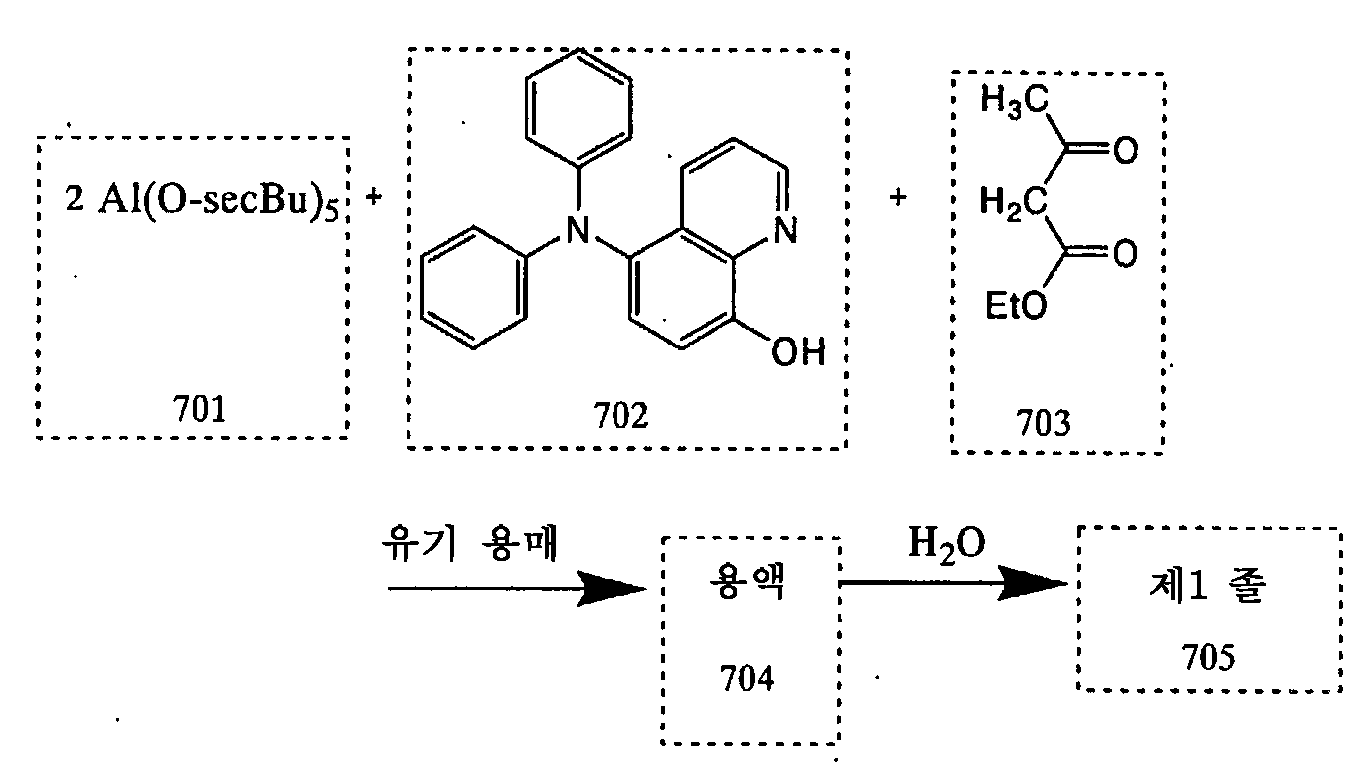


반응식 28은, 제1 금속 산화물의 금속 원자를 포함하는 금속 알콕사이드(701)(여기에서는 알루미늄 2급 부톡사이드), 본 발명의 복합 재료에 정공 주입성 또는 수송성을 제공하는 유기 화합물(702)(여기에서는 5-디페닐아미노-8-퀴놀리놀) 및 안정화제(703)(여기에서는 에틸 아세토아세테이트)를 2:1:1[단위: mmol]의 비율로 적당한 유기 용매에 용해시키고 반응시켜 용액(704)을 제조하고, 물을 첨가하여 가수분해시켜 제1 졸(705)을 얻는 경로를 나타낸 것이다. 이때, 유기 용매로서는, 예를 들면, 메탄올, 에탄올, n-프로판올, i-프로판올, n-부탄올, 2급 부탄올 등의 저급 알콜 이외에, THF, 아세토니트릴, 디클로로메탄, 디클로로에탄 또는 이들의 혼합 용매 등을 사용할 수 있지만, 이에 한정되는 것은 아니다. Reaction formula 28 is a reaction between a metal alkoxide 701 (here, aluminum secondary isotecoxide) containing a metal atom of the first metal oxide, an organic compound 702 that provides hole injectability or transportability to the composite material of the present invention (5-diphenylamino-8-quinolinol) and a stabilizer 703 (here, ethyl acetoacetate) in a proper organic solvent at a ratio of 2: 1: 1 [unit: mmol] 704) is prepared, and water is added to hydrolyze to obtain the first sol (705). Examples of the organic solvent include alcohols such as THF, acetonitrile, dichloromethane, dichloroethane, or a mixed solvent thereof such as methanol, ethanol, n-propanol, i-propanol, n-butanol, , But the present invention is not limited thereto.
또한, 유기 화합물(702)의 양은 금속 알콕사이드(701) 1mol에 대하여 0.1 mol 이상 1mol 이하인 것이 바람직하다. The amount of the organic compound (702) is preferably 0.1 mol or more and 1 mol or less with respect to 1 mol of the metal alkoxide (701).
또한, 안정화제(703)는, 물을 첨가하였을 때에, 급격한 중축합의 진행에 의한 침전의 생성을 억제하기 위한 것이지만, 유기 화합물(702)은 안정화제의 역할도 할 수 있기 때문에, 안정화제(703)가 반드시 필요한 것은 아니다. 그러나, 유기 화합물(702)의 양이 적은 경우(구체적으로는 금속 알콕사이드(701) 1mol에 대하여 0.5mol 이하), 안정화 능력이 손상되기 때문에, 안정화제(703)를 첨가하는 것이 바람직하다. 안정화제(703)로서는, β-디케톤, 디아민, 아미노알콜 등의 약한 킬레이트제가 바람직하고, 구체적으로는 반응식 28에 나타낸 에틸 아세토아세테이트 이외에, 아세틸아세톤, 벤조일아세톤, 에틸렌디아민, 모노에탄올아민 등을 들 수 있지만, 이들에 한정되는 것은 아니다. 안정화제(703)의 양은, 금속 알콕사이드(701) 1mol에 대하여 0.5mol 이상이면 효과를 발휘할 수 있다. 또한, 금속 알콕사이드(701)의 금속은 6가 이하이기 때문에, 안정화제(703)의 첨가량은 금속 알콕사이드(701) 1mol에 대하여 6mol 이하인 것이 바람직하다. The stabilizer 703 is intended to suppress the formation of precipitation due to the progress of the rapid polycondensation when water is added. Since the organic compound 702 can also serve as a stabilizer, the stabilizer 703 ) Is not necessarily required. However, when the amount of the organic compound 702 is small (more specifically, 0.5 mol or less with respect to 1 mol of the metal alkoxide 701), the stabilizing agent 703 is preferably added because the stabilizing ability is impaired. As the stabilizer 703, a weak chelating agent such as? -Diketone, diamine and amino alcohol is preferable. Specifically, acetylacetone, benzoyl acetone, ethylenediamine, monoethanolamine and the like can be used in addition to the acetoacetate shown in the reaction formula But the present invention is not limited thereto. When the amount of the stabilizer 703 is 0.5 mol or more with respect to 1 mol of the metal alkoxide 701, the effect can be exhibited. Further, since the amount of the metal alkoxide 701 is 6 or less, the addition amount of the stabilizer 703 is preferably 6 mol or less with respect to 1 mol of the metal alkoxide 701.
가수분해에 사용하는 물의 첨가량으로서는, 금속 알콕사이드(701)의 금속이 2가 내지 6가이기 때문에, 금속 알콕사이드(701) 1 mol에 대하여 2mol 이상 6mol 이하인 것이 바람직하다. 그러나, 가수분해는 반드시 필요하지는 않다. The amount of water to be used for hydrolysis is preferably 2 mol or more and 6 mol or less with respect to 1 mol of the metal alkoxide 701 since the metal of the metal alkoxide 701 is from 2 to 6. However, hydrolysis is not necessarily required.
반응식 29는, 제2 금속 산화물의 금속 원자를 포함하는 금속 알콕사이드(706)(여기에서는 펜타에톡시 몰리브덴(V))과 안정화제(707)(여기에서는 에틸 아세토아세테이트)를 1:1[단위: mol]의 비율로 적당한 유기 용매에 용해시키고 반응시켜 용액(708)을 제조하고, 물을 첨가하여 가수분해시켜 제2 졸(709)을 얻는 경로를 나타낸 것이다. 이때, 유기 용매로서는, 제1 졸(705)과 같은 용매를 사용할 수 있다. Reaction Scheme 29 shows the reaction of a metal alkoxide 706 (herein, pentaethoxymolybdenum (V)) containing a metal atom of a second metal oxide and a stabilizer 707 (here, ethyl acetoacetate) in a ratio of 1: mol] in a suitable organic solvent and reacted to prepare a solution 708, followed by hydrolysis by adding water to obtain a second sol 709. As the organic solvent, a solvent such as the first sol 705 may be used.
가수분해에 사용하는 물의 첨가량으로서는, 금속 알콕사이드(706)의 금속이 2가 내지 6가이기 때문에, 금속 알콕사이드(706) 1mol에 대하여 2mol 이상 6mol 이하인 것이 바람직하다. 그러나, 가수분해는 반드시 필요하지는 않다. The amount of water to be used for the hydrolysis is preferably 2 mol or more and 6 mol or less with respect to 1 mol of the metal alkoxide 706 since the metal of the metal alkoxide 706 is from 2 to 6. However, hydrolysis is not necessarily required.
또한, 안정화제(707)는, 가수분해를 하지 않은 경우는 반드시 필요하지는 않다. 안정화제(707)로서는 상술한 물질을 사용할 수 있다. 안정화제(707)의 양은 금속 알콕사이드(706) 1mol에 대하여 0.5mol 이상이면 효과를 발휘할 수 있다. 또한, 금속 알콕사이드(706)의 금속은 6가 이하이기 때문에, 안정화제(707)의 첨가량은 금속 알콕사이드(706) 1mol에 대하여 6mol 이하인 것이 바람직하다. Further, the stabilizer 707 is not necessarily required when hydrolysis is not performed. As the stabilizer 707, the above-mentioned materials can be used. The amount of the stabilizer (707) is 0.5 mol or more with respect to 1 mol of the metal alkoxide (706). Further, since the amount of the metal alkoxide 706 is 6 or less, the addition amount of the stabilizer 707 is preferably 6 mol or less with respect to 1 mol of the metal alkoxide 706.
반응식 30은, 제1 졸(705)과 제2 졸(709)을 혼합하여, 제3 졸(710)을 얻는 경로를 나타낸 것이다. 이때, 제3 졸(710)에 있어서, 유기 화합물(702)의 양은 제2 금속 알콕사이드(706)의 금속 1mol에 대하여 0.1mol 이상 10mol 이하로 되도록 혼합하는 것이 바람직하다. 또한, 복합 재료로서, 제3 금속 산화물을 추가로 첨가한 복합 재료를 제조하는 경우, 제3 졸(710)에 대하여, 제3 금속 산화물의 금속을 포함하는 제3 금속 알콕사이드를 첨가할 수 있다. 이때, 상술한 안정화제를 적절히 첨가할 수 있다. 또한, 제3 금속 산화물로서 산화규소를 적용하는 경우, 제3 금속 알콕사이드로서 테트라알콕시실란을 사용할 수 있지만, 이때 제3 금속 알콕사이드를 산성 또는 알칼리성으로 되도록 하는 것이 바람직하다. 보다 바람직하게는, pH 1 내지 3의 산성이다. The reaction formula 30 shows a path for obtaining the third sol 710 by mixing the first sol 705 and the second sol 709. [ In this case, the amount of the organic compound 702 in the third sol 710 is preferably 0.1 mol or more and 10 mol or less with respect to 1 mol of the metal of the second metal alkoxide 706. Further, in the case of producing a composite material in which a third metal oxide is further added as a composite material, a third metal alkoxide containing a metal of a third metal oxide may be added to the third sol 710. At this time, the stabilizer described above can be suitably added. Further, when silicon oxide is used as the third metal oxide, tetraalkoxysilane may be used as the third metal alkoxide, but it is preferable that the third metal alkoxide is made acidic or alkaline. More preferably, it is acidic with a pH of 1 to 3.
반응식 31은, 위에서 얻어진 제3 졸(710)을 도포하고 소성하여 본 발명의 복합 재료(711)를 얻는 공정을 나타낸 것이다. 또한, 상기 공정으로서는, 제3 졸을 기재상에 습식 도포한 후, 100℃ 이상 300℃ 이하의 온도에서 상압하에 또는 감압하에 소성하는 방법을 사용할 수 있다. 소성은 대기 중에서 또는 불활성 기체(질소, 아르곤등) 중에서 수행될 수 있다. 또한, 제3 졸(710)이 안정화제를 포함하는 경우, 소성에 의해 안정화제를 제거하는 것이 바람직하다. Reaction Equation 31 shows a process for obtaining the composite material 711 of the present invention by applying and firing the third sol 710 obtained above. As the above step, a method in which the third sol is wet-coated on a substrate and then baked at a temperature of 100 ° C or more and 300 ° C or less under atmospheric pressure or reduced pressure may be used. The calcination can be carried out in the air or in an inert gas (nitrogen, argon, etc.). Further, when the third sol 710 contains a stabilizer, it is preferable to remove the stabilizer by firing.
또한, β-디케톤(여기에서는 에틸 아세토아세테이트)을 안정화제(703)로서 첨가하는 경우, 제3 졸을 기재상에 습식 도포한 후, β-디케톤이 금속 원자에 리간드로서 결합된 상태의 자외선 흡수 스펙트럼과 중첩되는 파장의 자외선을 조사하여, β-디케톤을 해리시키는 방식으로 겔화를 진행시킬 수 있다. 그 후, 상술한 바와 같은 방식으로 소성함으로써, 본 발명의 복합 재료(711)를 얻을 수 있다. When β-diketone (here, ethyl acetoacetate) is added as the stabilizer 703, the third sol is wet-coated on the substrate, and then β-diketone is bonded to the metal atom as a ligand The gelation can be promoted by irradiating ultraviolet rays having a wavelength overlapping with the ultraviolet absorption spectrum to dissociate? -Diketone. Thereafter, the composite material 711 of the present invention can be obtained by firing in the above-described manner.
또한, 반응식 28 또는 반응식 29에서 가수분해하지 않은 경우, 제3 졸(710)을 직접 기재상에 습식 도포하고, 건조시킨 후, 수증기로 가수분해시킬 수 있다. 그 후, 상술한 바와 같은 방식으로 소성함으로써, 본 발명의 복합 재료(711)를 얻을 수 있다. Further, in the case where the hydrolysis is not performed in Reaction Formula 28 or Reaction Formula 29, the third sol 710 may be directly applied on the substrate by wet application, followed by drying and hydrolysis by steam. Thereafter, the composite material 711 of the present invention can be obtained by firing in the above-described manner.
여기에서, 상술한 습식 도포법으로서는, 침지 도포법, 스핀 도포법, 잉크젯법 등을 사용할 수 있지만, 이들에 한정되는 것은 아니다. Here, as the above-mentioned wet coating method, an immersion coating method, a spin coating method, an ink jet method, or the like can be used, but the present invention is not limited thereto.
(실시 형태 8) (Embodiment 8)
본 실시 형태로서는, 실시 형태 3 또는 4에서 기재한 바와 같은 본 발명의 복합 재료를, 금속 알콕사이드를 사용하고 해교도 이용하는 졸-겔법에 의해 제조하는 방법에 관해서 설명한다. In this embodiment mode, a method of producing the composite material of the present invention as described in
상기 방법의 도식을 하기 반응식 32 내지 35에 나타낸다. 또한, 본 실시 형태로서는, 제1 금속 산화물 골격으로서 알루미늄 산화물 골격, 정공 주입성 또는 수송성을 갖고 알루미늄 원자에 킬레이트 리간드로서 결합될 수 있는 유기 화합물로서 5-디페닐아미노-8-퀴놀리놀, 및 유기 화합물에 대하여 전자 수용성을 나타내는 제2 금속 산화물로서 몰리브덴 산화물을, 각각 사용한 복합 재료(실시 형태 3)를 제조하는 경우를 예로서 설명한다. 다른 금속 산화물 골격을 사용하는 경우, 2종 이상의 금속을 갖는 금속 산화물 골격을 사용하는 경우, 및 다른 유기 화합물을 사용하는 경우도, 기본원리는 모두 같다. Scheme of the above method is shown in the following Reaction Schemes 32 to 35. In this embodiment mode, 5-diphenylamino-8-quinolinol as an organic compound having an aluminum oxide skeleton, a hole injecting property or transportability and being capable of bonding as a chelate ligand to an aluminum atom as a first metal oxide skeleton, and (Embodiment 3) using molybdenum oxide as a second metal oxide showing an electron-accepting property with respect to an organic compound will be described as an example. The basic principle is the same in the case of using different metal oxide skeletons, the case of using a metal oxide skeleton having two or more kinds of metals, and the case of using other organic compounds.


반응식 32는, 제1 금속 산화물의 금속 원자를 포함하는 금속 알콕사이드(801)(여기에서는 알루미늄 2급 부톡사이드), 본 발명의 복합 재료에 정공 주입성 또는 수송성을 제공하는 유기 화합물(802)(여기에서는 5-디페닐아미노-8-퀴놀리놀) 및 안정화제(803)(여기에서는 에틸 아세토아세테이트)를 2:1:1[단위: mmol]의 비율로 적당한 유기 용매에 용해시키고 반응시켜 용액(804)을 제조하고, 물을 첨가하여 가수분해시켜 제1 졸(805)을 얻는 경로를 나타낸 것이다. 이때, 유기 용매로서는, 예를 들면, 메탄올, 에탄올, n-프로판올, i-프로판올, n-부탄올, 2급 부탄올 등의 저급 알콜 이외에, THF, 아세토니트릴, 디클로로메탄, 디클로로에탄 및 이들의 혼합 용매 등을 사용할 수 있지만, 이에 한정되는 것은 아니다. The reaction formula 32 is a reaction between the metal alkoxide 801 (here, aluminum sec-butoxide) containing the metal atom of the first metal oxide, the organic compound 802 that provides hole injectability or transportability to the composite material of the present invention (5-diphenylamino-8-quinolinol) and a stabilizer (803) (here, ethyl acetoacetate) were dissolved in a proper organic solvent at a ratio of 2: 1: 1 804) is prepared, and water is added to hydrolyze to obtain the first sol (805). Examples of the organic solvent include alcohols such as THF, acetonitrile, dichloromethane, dichloroethane and mixed solvents thereof such as methanol, ethanol, n-propanol, i-propanol, n-butanol, , But the present invention is not limited thereto.
또한, 유기 화합물(802)의 양은 금속 알콕사이드(801) 1mol에 대하여 0.1mol 이상 1mol 이하인 것이 바람직하다. The amount of the organic compound (802) is preferably 0.1 mol or more and 1 mol or less with respect to 1 mol of the metal alkoxide (801).
또한, 안정화제(803)는, 물을 첨가하였을 때, 급격한 중축합의 진행에 의한 침전의 생성을 억제하기 위한 것이지만, 유기 화합물(802)은 안정화제의 역할도 할 수 있기 때문에, 안정화제(803)는 반드시 필요하지는 않다. 그러나, 유기 화합물(802)의 양이 적은 경우(구체적으로는 금속 알콕사이드(801) 1mol에 대하여 0.5mol 이하), 안정화 능력이 손상되기 때문에, 안정화제(803)를 첨가하는 것이 바람직하다. 안정화제(803)로서는, β-디케톤, 디아민, 아미노알콜 등의 약한 킬레이트제가 바람직하고, 구체적으로는 반응식 32에 나타낸 에틸 아세토아세테이트이외에, 아세틸아세톤, 벤조일아세톤, 에틸렌디아민, 모노에탄올아민 등을 들 수 있지만, 이들에 한정되는 것은 아니다. 안정화제(803)의 양은 금속 알콕사이드(801) 1mol에 대하여 0.5mol 이상이면 효과를 발휘할 수 있다. 또한, 금속 알콕사이드(801)의 금속은 6가 이하이기 때문에, 안정화제(803)의 첨가량은 금속 알콕사이드(801) 1mol에 대하여 6mol 이하인 것이 바람직하다. The stabilizer 803 is intended to suppress the formation of precipitates due to the progress of rapid polycondensation when water is added. Since the organic compound 802 can also serve as a stabilizer, the stabilizer 803 ) Is not necessarily required. However, when the amount of the organic compound 802 is small (more specifically, 0.5 mol or less with respect to 1 mol of the metal alkoxide 801), the stabilizing agent 803 is preferably added because the stabilizing ability is impaired. As the stabilizer 803, a weak chelating agent such as? -Diketone, diamine, and amino alcohol is preferable. Specifically, acetylacetone, benzoyl acetone, ethylenediamine, monoethanolamine and the like are used in addition to the acetoacetate shown in the reaction formula But the present invention is not limited thereto. The effect of the stabilizer (803) can be exhibited when the amount of the stabilizer (803) is 0.5 mol or more with respect to 1 mol of the metal alkoxide (801). The amount of the stabilizer 803 to be added is preferably 6 mol or less with respect to 1 mol of the metal alkoxide 801 since the metal alkoxide 801 has 6 or less metals.
가수분해에 사용하는 물의 첨가량으로서는, 금속 알콕사이드(801)의 금속이 2가 내지 6가이기 때문에, 금속 알콕사이드(801) 1mol에 대하여 2mol 이상 6mol 이하가 바람직하다. 그러나, 가수분해는 반드시 필요하지는 않다. The amount of water to be used for hydrolysis is preferably 2 mol or more and 6 mol or less based on 1 mol of the metal alkoxide (801) since the metal of the metal alkoxide (801) is 2 to 6 molar equivalents. However, hydrolysis is not necessarily required.
반응식 33은, 제2 금속 산화물의 금속 원자를 포함하는 금속 염화물(806)(여기에서는 염화몰리브덴(V))의 용액에 암모니아수를 적하하여 금속 수산화물의 다핵 침전(807)을 얻고, 이어서 아세트산 등의 산을 가하여 환류(해교)함으로써 제2 졸(808)을 얻는 방법을 나타내고 있다. 제2 졸(808)에는, 적당한 유기 용매를 적절히 첨가할 수 있다. Scheme 33 shows a method in which ammonia water is dropped into a solution of a metal chloride 806 (here, molybdenum chloride (V)) containing a metal atom of a second metal oxide to obtain a polynuclear precipitation 807 of metal hydroxide, And an acid is added to reflux (peptism) to obtain the second sol 808. To the second sol 808, a suitable organic solvent can be appropriately added.
반응식 34은, 제1 졸(805)과 제2 졸(808)을 혼합하여, 제3 졸(809)을 얻는 경로를 나타낸 것이다. 이때, 제3 졸(809)에 있어서, 유기 화합물(802)의 양은 제2 졸(808)에 포함되는 금속 1mol에 대하여 0.1mol 이상 10mol 이하로 되도록 혼합하는 것이 바람직하다. 또한, 복합 재료로서, 제3 금속 산화물을 추가로 첨가한 복합 재료를 제조하는 경우, 제3 졸(809)에 대하여, 제3 금속 산화물의 금속을 포함하는 제3 금속 알콕사이드를 첨가할 수 있다. 이때, 상술한 안정화제를 적절히 추가로 첨가할 수 있다. 또한, 제3 금속 산화물로서 산화규소를 적용하는 경우, 제3 금속 알콕사이드로서 테트라알콕시실란을 사용할 수 있지만, 이 경우에 제3 졸(809)을 산성 또는 알칼리성으로 되도록 하는 것이 바람직하다. 보다 바람직하게는, pH 1 내지 3의 산성이다. The equation (34) shows a path in which the first sol 805 and the second sol 808 are mixed to obtain the third sol 809. At this time, in the third sol 809, the amount of the organic compound 802 is preferably 0.1 mol or more and 10 mol or less with respect to 1 mol of the metal contained in the second sol 808. In the case of producing a composite material in which a third metal oxide is further added as a composite material, a third metal alkoxide containing a metal of a third metal oxide may be added to the third sol 809. At this time, the above stabilizers can be appropriately added. When silicon oxide is used as the third metal oxide, tetraalkoxysilane can be used as the third metal alkoxide, but in this case, it is preferable to make the third sol 809 acidic or alkaline. More preferably, it is acidic with a pH of 1 to 3.
반응식 35는, 위에서 얻어진 제3 졸(809)을 도포하고 소성하여 본 발명의 복합 재료(810)를 얻는 공정을 나타낸 것이다. 또한, 상기 공정으로서는, 제3 졸(809)을 기재상에 습식 도포한 후, 100℃ 이상 300℃ 이하의 온도에서 상압하에 또는 감압하에 소성하는 방법을 사용할 수 있다. 소성분은 대기 중에서 또는 불활성 기체(질소, 아르곤등) 중에서 수행될 수 있다. 또한, 제3 졸(809)이 안정화제를 포함하는 경우, 소성에 의해 안정화제를 제거하는 것이 바람직하다. The reaction formula (35) shows a step of obtaining the composite material (810) of the present invention by coating and firing the third sol (809) obtained above. As the above step, a method in which the third sol 809 is wet-coated on a substrate and then fired at a temperature of 100 ° C or more and 300 ° C or less under atmospheric pressure or reduced pressure can be used. The small component may be carried out in the air or in an inert gas (nitrogen, argon, etc.). Further, when the third sol 809 contains a stabilizer, it is preferable to remove the stabilizer by firing.
또한, β-디케톤(여기에서는 에틸 아세토아세테이트)을 안정화제로서 첨가하는 경우, 제3 졸을 기재상에 습식 도포한 후, β-디케톤이 금속 원자에 리간드로서 결합된 상태의 자외선 흡수 스펙트럼과 중첩된 파장의 자외선을 조사하여, β-디케톤을 해리시키는 방식으로 겔화를 진행시킬 수 있다. 그 후, 상술한 바와 같은 방식으로 소성함으로써, 본 발명의 복합 재료(810)를 얻을 수 있다. Further, in the case where? -Diketone (here, ethyl acetoacetate) is added as a stabilizer, the third sol is wet-coated on the substrate, and ultraviolet absorption spectrum in the state where? -Diketone is bonded as a ligand to the metal atom And ultraviolet rays of superimposed wavelengths are irradiated to the gel, and the gelation can proceed by dissociating? -Diketone. Thereafter, the composite material 810 of the present invention can be obtained by firing in the above-described manner.
또한, 반응식 32에서 가수분해시키지 않은 경우, 제3 졸(809)을 직접 기재상에 습식 도포하고, 건조시킨 후, 수증기로 가수분해시킬 수 있다. 그 후, 상술한 바와 같은 방식으로 소성함으로써, 본 발명의 복합 재료(810)를 얻을 수 있다. In addition, in the case of not hydrolyzing in Reaction Equation 32, the third sol 809 can be wet applied directly onto the substrate, dried and hydrolyzed with steam. Thereafter, the composite material 810 of the present invention can be obtained by firing in the above-described manner.
여기에서, 상술한 습식 도포법으로서는, 침지 도포법, 스핀 도포법, 잉크젯법 등을 사용할 수 있지만, 이들에 한정되는 것은 아니다. Here, as the above-mentioned wet coating method, an immersion coating method, a spin coating method, an ink jet method, or the like can be used, but the present invention is not limited thereto.
(실시 형태 9) (Embodiment 9)
계속해서 본 발명의 발광 소자에 관해서 설명한다. 본 발명의 발광 소자는 전자 주입층, 전자 수송층, 정공 주입층 및 정공 수송층으로 대표되는 각 기능층의 1층 이상이, 실시 형태 1 내지 실시 형태 4로 나타낸 본 발명의 복합 재료에 의해 형성된 발광 소자이다. Next, the light emitting device of the present invention will be described. The light emitting device of the present invention is characterized in that one or more of the functional layers represented by the electron injecting layer, the electron transporting layer, the hole injecting layer, and the hole transporting layer are formed of the light emitting element formed by the composite material of the present invention shown in
본 발명의 발광 소자는 상기 복합 재료에 의해 형성된 층 뿐만 아니라, 적어도 발광 물질을 포함하는 발광층을 포함하며, 이들 층들은 발광 소자를 구성하는 한 쌍의 전극 사이에 삽입되어 있다. 전압을 인가함에 따라 발광층으로부터 발광을 얻을 수 있다. The light emitting device of the present invention includes not only a layer formed by the composite material but also a light emitting layer including at least a light emitting material, and these layers are inserted between a pair of electrodes constituting the light emitting element. When a voltage is applied, light emission can be obtained from the light emitting layer.
이러한 구성을 갖는 본 발명의 발광 소자는, 전자 주입층, 전자 수송층, 정공 주입층 및 정공 수송층으로 대표되는 각 기능층의 1층 이상이 금속 산화물 골격을 갖는 본 발명의 복합 재료에 의해 형성되기 때문에 내열성이 우수한 발광 소자일 수 있고, 장시간 안정하게 구동될 수 있는 발광 소자일 수 있다. Since the light emitting device of the present invention having such a structure is formed by the composite material of the present invention having one or more layers of the functional layers typified by the electron injection layer, the electron transport layer, the hole injection layer and the hole transport layer, The light emitting device can be a light emitting device having excellent heat resistance and can be stably driven for a long time.
또한, 상기 복합 재료는, 전자 또는 정공 주입성 또는 수송성을 갖는 유기 화합물과, 상기 유기 화합물로부터 전자를 수용하거나 유기 화합물에 전자를 공여할 수 있는 금속 산화물이 포함되어 있기 때문에, 복합 재료의 전도성 및 캐리어 주입성 또는 수송성이 향상된다. In addition, since the composite material includes an organic compound having electrons or holes injecting or transporting ability and a metal oxide capable of accepting electrons from the organic compound or donating electrons to the organic compound, The carrier injectability or transportability is improved.
또한, 본 발명의 발광 소자는, 전자 또는 정공 주입성 또는 수송성을 갖는 유기 화합물과, 상기 유기 화합물로부터 전자를 수용하거나 유기 화합물에 전자를 공여할 수 있는 금속 산화물이 포함되어 있는 복합 재료를 사용하기 때문에, 내열성이 우수한 발광 소자, 장시간 안정하게 구돌될 수 있는 발광 소자, 또는 내열성이 우수하고 장시간 안정하게 구동될 수 있는 발광 소자일 수 있어서, 소비전력이 작은 발광 소자를 제조하는 것이 가능하다. Further, the light-emitting device of the present invention uses a composite material containing an organic compound having electrons or holes injecting or transporting ability and a metal oxide capable of accepting electrons from the organic compound or donating electrons to the organic compound Therefore, it is possible to manufacture a light emitting element having excellent heat resistance, a light emitting element which can be stably held for a long time, or a light emitting element which is excellent in heat resistance and can be stably driven for a long time.
또한, 본 발명의 발광 소자의 상기 기능층 중의 1층은 복합 재료로 형성되지 않고 다른 재료에 의해 추가로 형성될 수도 있다. 이 경우에도 내열성 및 내구성에 가장 문제가 있는 층을 복합 재료로 형성함으로써 내열성 및 내구성을 향상시킬 수 있다. In addition, one of the functional layers of the light emitting device of the present invention may not be formed of a composite material but may be additionally formed of another material. Also in this case, heat resistance and durability can be improved by forming a layer having the most problems in heat resistance and durability from a composite material.
또한, 본 발명의 복합 재료를 기능층으로서 형성한 발광 소자는 기능층의 막 두께를 두껍게 형성하더라도 구동 전압의 상승이 적다. 따라서, 발광 소자의 한 쌍의 전극 중, 먼저 형성되는 쪽의 전극과 발광층 사이의 기능층의 막 두께를 두껍게 형성할 수 있어, 분진 등에 의한 발광 소자의 단락이 일어나는 것을 감소시킬 수 있다. 막 두께가 100nm 이상이면 이러한 결함을 유효하게 감소시킬 수 있다. Further, the light emitting device in which the composite material of the present invention is formed as a functional layer has a small increase in driving voltage even when the thickness of the functional layer is increased. Therefore, the thickness of the functional layer between the electrode on the first pair of electrodes of the light emitting element and the light emitting layer can be made thick, and the short circuit of the light emitting element due to dust or the like can be reduced. If the film thickness is 100 nm or more, such defects can be effectively reduced.
두께가 두꺼운 기능층은 전자 또는 정공 주입성 또는 수송성을 갖는 유기 화합물과, 상기 유기 화합물로부터 전자를 수용하고 유기 화합물에 전자를 공여할 수 있는 금속 산화물이 포함되어 있는 본 발명의 복합 재료를 포함하기 때문에, 전도성 및 캐리어 주입성 또는 수송성이 향상되어, 구동 전압을 대폭 상승시키지 않고, 즉 소비전력을 대폭 증대하지 않으면서 분진 등에 의한 발광 소자의 단락이 일어나는 것을 감소시킬 수 있다. The thick functional layer includes the composite material of the present invention containing an organic compound having electrons or holes injecting or transporting property and a metal oxide capable of accepting electrons from the organic compound and donating electrons to the organic compound Therefore, conductivity and carrier injection ability or transportability are improved, and it is possible to reduce occurrence of short circuit of the light emitting element by dust or the like without significantly increasing the driving voltage, that is, by not significantly increasing the power consumption.
또한, 본 발명의 발광 소자는 전자 주입층, 전자 수송층, 정공 주입층 및 정공 수송층으로 대표되는 기능층의 1층이 복합 재료에 의해 형성될 수 있거나, 2 이상의 기능층이 복합 재료에 의해 형성될 수도 있다. 또한, 상기 기능층 모두가 복합 재료에 의해 형성될 수 있다. 또한, 발광층도 금속 산화물 골격 중의 금속 원자에 킬레이트 리간드로서 결합된 유기 화합물을 포함하는 복합 재료로 형성할 수 있다. 발광층을 복합 재료에 의해 형성하는 경우, 내열성이 우수하고 장시간 안정하게 구동될 수 있는 발광 소자를 제조할 수 있다. 이때, 전압을 인가함으로써 발광하는 유기 화합물과 금속 산화물의 원료를 포함하는 졸을, 발광층을 형성하고 싶은 표면에 도포하고 소성시킴으로서, 발광층을 형성할 수 있다. 예를 들면, 금속 산화물 골격 중의 금속 원자에, 전압을 인가함으로써 발광하는 유기 화합물이 킬레이트 리간드로서 결합된 발광층을 형성할 수 있다. 또한, 졸의 제조방법에 관해서는 본 발명의 실시 형태 7에 있어서의 제1 졸(705)의 제조방법에 준하고, 도포 및 소성방법은 본 발명의 복합 재료의 도포 및 소성방법에 준한다. 이에 의해 금속 산화물 골격을 갖는 발광층을 제조할 수 있다. In the light emitting device of the present invention, one layer of the functional layer typified by the electron injecting layer, the electron transporting layer, the hole injecting layer and the hole transporting layer may be formed of a composite material, or two or more functional layers may be formed of a composite material It is possible. Further, both of the functional layers may be formed of a composite material. Further, the light emitting layer can also be formed of a composite material containing an organic compound bonded as a chelate ligand to a metal atom in the metal oxide skeleton. When the light emitting layer is formed of a composite material, a light emitting device that is excellent in heat resistance and can be stably driven for a long time can be manufactured. At this time, a light-emitting layer can be formed by applying a sol containing a raw material of an organic compound and a metal oxide that emits light by applying a voltage to a surface on which a light-emitting layer is to be formed and baking. For example, a light emitting layer in which an organic compound emitting light by applying a voltage to a metal atom in a metal oxide framework is bonded as a chelate ligand can be formed. The method of manufacturing the sol is the same as that of the first sol (705) in the seventh embodiment of the present invention, and the coating and firing methods are the same as those of the application and firing of the composite material of the present invention. Thus, a light emitting layer having a metal oxide framework can be produced.
계속해서 본 발명의 발광 소자예의 모식도를 도 19A와 도 19B 및 도 20A와 도 20B에 나타낸다. 도 19A에 있어서, 기판 등의 절연 표면(200)에 제1 전극(201)이 형성되고, 그 위에 본 발명의 복합 재료로 형성된 정공 주입 및/또는 수송층(202)(정공 주입층과 정공 수송층으로 분리될 수 있다), 발광층(203), 본 발명의 복합 재료로 형성된 전자 주입 및/또는 수송층(204)(전자 주입층과 전자 수송층으로 분리될 수 있다)가 순차로 적층되어 있다. 또한, 그 위에는 발광 소자의 제2 전극(205)이 제공되고, 상기 발광 소자를 구동하는 경우에는 제1 전극(201)이 제2 전극(205)보다 전위가 높도록 전압을 인가하여(즉, 제1 전극(201)이 애노드로서 기능하고, 제2 전극(205)이 캐소드로서 기능한다) 발광이 얻어지는 구조로 되어있다. Subsequently, a schematic diagram of a light emitting device example of the present invention is shown in Figs. 19A and 19B and Figs. 20A and 20B. 19A, a
발광층(203)은, 증착법에 의해 형성될 수 있거나, 상술한 바와 같은 전압을 인가함으로써 발광하는 유기 화합물 및 금속 산화물 골격을 포함하는 복합 재료로부터 형성될 수도 있다. The
상기 구성으로서는 정공 주입 및/또는 운송층(202)과 전자 주입 및/또는 수송층(204)의 양쪽을 본 발명의 복합 재료에 의해 형성하였다. 그러나, 어떤 층이든 본 발명의 복합 재료로 형성할 수 있다. In the above structure, both the hole injecting and / or transporting
또한, 본 발명의 복합 재료로 형성하지 않은 층에 관해서는, 공지된 재료로, 증착법 등의 공지된 방법에 의해 형성할 수 있다. The layer not formed of the composite material of the present invention can be formed by a known method such as a vapor deposition method.
도 19A에 도시한 바와 같은 발광 소자는 내열성이 우수하고 장기간 안정하게 구동될 수 있는 발광 소자일 수 있다. The light emitting device as shown in FIG. 19A may be a light emitting device that has excellent heat resistance and can be stably driven for a long period of time.
도 19B는, 도 19A에 있어서의 정공 주입 및/또는 수송층(202)을 두껍게 형성한 정공 주입 및/또는 수송층(206)을 갖는 발광 소자의 모식도이다. 그 밖의 층은 도 19A와 같기 때문에 설명을 생략한다. 발광 소자는 매우 엷은 박막을 적층함으로써 형성된다. 하부에 형성된 제1 전극(201)에 곡률이 작고 높이가 높은 볼록한 부분(분진 또는 하부의 요철로 인한 것으로 여겨진다)이 존재하는 경우, 볼록한 부분은 박막으로 완전히 덮이지 않으므로, 이러한 박막은 단락과 같은 결함을 발생시킨다. 한편, 이를 방지하기 위하여 막을 두껍게 형성하는 경우, 발광 소자는 저항이 증가하여, 구동 전압이 상승하는 단점이 있다. 그러나, 본 발명의 복합 재료는, 전자 또는 정공 주입성 또는 수송성을 갖는 유기 화합물과, 상기 유기 화합물로부터 전자를 수용하거나 상기 유기 화합물에 전자를 공여할 수 있는 금속 산화물을 포함하고 있기 때문에, 전도성이 높아, 막이 두껍더라도 저항의 상승을 억제할 수 있다. 또한, 도 19B의 구성을 갖는 발광 소자는 기본적으로 도 19A의 구성을 갖고 있기 때문에, 내열성이 우수하고 장기간 안정하게 구동될 수 있는 발광 소자이다. 따라서, 도 19B의 구성을 갖는 본 발명의 발광 소자는 내열성이 우수하고 장기간 안정하게 구동될 수 있고, 결함이 적은 발광 소자이다. 19B is a schematic diagram of a light emitting device having a hole injecting and / or transporting
도 20A는 도 19A에 있어서의 전자 주입 및/또는 수송층(204)과 제2 전극(205)의 사이에, 본 발명의 복합 재료로 형성된 정공 주입 및/또는 수송층(207)을 형성하는 예를 도시한 것이다. 본 발명의 복합 재료로 형성된 정공 주입 및/또는 수송층(207)은 복합 재료 중의 유기 화합물로서, 정공 주입성 또는 수송성이 우수한 유기 화합물을 사용하고, 상기 유기 화합물로부터 전자를 수용할 수 있는 물질을 추가로 포함하는 복합 재료, 즉 정상 환경하에 정공 주입층 또는 정공 수송층으로서 사용되는 재료로 형성되어 있다. 20A shows an example in which a hole injecting and / or transporting
그러나, 발광층(203)을 기준으로 캐소드로서 작용하는 전극(제2 전극(205))측에, 본 발명의 복합 재료로 형성된 전자 주입 및/또는 수송층(204)과 본 발명의 복합 재료로 형성된 정공 주입 및/또는 수송층(207)을 순차로 적층함으로써, 전압을 인가하는 경우, 본 발명의 복합 재료로 형성된 전자 주입 및/또는 수송층(204)에서 전자가 발생하여 발광층(203)에 주입되고, 본 발명의 복합 재료로 형성된 정공 주입 및/또는 수송층(207)에서 정공이 발생하여 캐소드로서 작용하는 전극(제2 전극(205))에 주입됨으로써 전류가 흘러, 발광을 얻을 수 있다. However, the electron injecting and / or transporting
또한, 이러한 구조를 발광층(203)을 기준으로 애노드로서 작용하는 전극측에 형성하는 경우, 동일한 방식으로 전자 주입 및/또는 수송층으로서 사용될 수 있는 본 발명의 복합 재료에 의한 층과 정공 주입 및/또는 수송층으로서 사용될 수 있는 본 발명의 복합 재료에 의한 층을 순차로 적층함으로써 형성할 수 있다. 또한, 이러한 구조는 발광층(203)을 기준으로 하여 캐소드로서 작용하는 전극(제2 전극(205))측 및 애노드로서 작용하는 전극(제1 전극(201))측의 어느 한쪽에도 제공할 수 있고, 양쪽에 제공할 수도 있다. Further, when such a structure is formed on the electrode side acting as an anode on the basis of the
이러한 구성을 갖는 발광 소자는 제1 전극(201) 또는 제2 전극(205)으로서, 일함수를 고려하지 않고 재료를 선택할 수 있어, 반사 전극이나 투명 전극 등의 구조에 따라 보다 적합한 전극을 선택할 수 있다. The light emitting device having such a configuration can be selected as the
도 20B는 백색 발광을 제공할 수 있는 발광 소자의 예를 도시한 것이다. 도 19A에 있어서의 정공 주입 및/또는 수송층(202)과 전자 주입 및/또는 수송층(204)의 사이에 제1 발광층(208), 간격층(209), 제2 발광층(210)이 제공되어 있다. 제1 발광층(208)과 제2 발광층(210)의 재료는 적색과 청색 등의 서로 보색 관계를 갖는 발광색을 보이는 재료를 사용하여 백색 발광을 얻을 수 있다. 20B shows an example of a light emitting element capable of providing white light emission. A first
간격층(209)은 정공 수송성 재료, 전자 수송성 재료, 양극성(bipolar) 재료, 정공 차단성 재료, 캐리어 발생 재료 등에 의해 형성할 수 있어, 투광성을 갖는 것이 조건이다. 간격층(209)은 제1 발광층(208) 또는 제2 발광층(210)이 에너지 이동에 의해 보다 강하게 발광하는 것을 방지할 목적으로 제공된다. 이러한 현상이 일어나지 않은 한, 특별히 간격층(209)을 마련할 필요가 없다. The
도 20B의 구성을 갖는 발광 소자는 백색 발광을 제공할 수 있고, 내열성이 우수하고 장시간 안정하게 구동될 수 있는 발광 소자이다. 이러한 소자는 조명 용도에 적합하게 사용할 수 있다. The light emitting element having the configuration of Fig. 20B is a light emitting element that can provide white light emission, has excellent heat resistance, and can be stably driven for a long time. These devices can be used for lighting applications.
또한, 본 실시 형태는 다른 실시 형태와 모순이 없는 한 조합하여 사용할 수 있다. The present embodiment can be used in combination as long as it does not contradict other embodiments.
(실시 형태 10) (Embodiment 10)
본 실시 형태로서는, 본 발명의 표시 장치에 관해서 도 11A 내지 도 11E 및 도 12A 내지 도 12C를 참조하여, 제조방법을 나타내면서 설명한다. 또한, 본 실시 형태로서는 능동 매트릭스형 표시 장치를 제조하는 예를 개시하였지만, 수동 매트릭스형 표시 장치이더라도 본 발명의 표시 장치를 적용할 수 있는 것은 물론이다. In the present embodiment, the display device of the present invention will be described with reference to Figs. 11A to 11E and Figs. 12A to 12C, showing the manufacturing method. Although the present embodiment discloses an example of manufacturing an active matrix type display device, it goes without saying that the display device of the present invention can be applied to a passive matrix type display device.
우선, 기판(50)상에 제1 기초 절연층(51a) 및 제2 기초 절연층(51b)을 형성한 후, 반도체 층을 제2 기초 절연층(51b) 상에 형성한다(도 11A). First, after forming the first insulating
기판(50)의 재료로서는 유리, 석영, 플라스틱(폴리이미드, 아크릴, 폴리에틸렌 테레프탈레이트, 폴리카보네이트, 폴리아크릴레이트, 폴리에테르설폰 등) 등을 사용할 수 있다. 이들 기판은 필요에 따라서 CMP 등에 의해 연마하고 나서 사용할 수 있다. 본 실시 형태에 있어서는 유리 기판을 사용한다. As the material of the
제1 기초 절연층(51a) 및 제2 기초 절연층(51b)는 기판(50) 중의 알칼리 금속이나 알칼리 토금속 등의 반도체막의 특성에 악영향을 미치는 원소가 반도체 층 중에 확산하는 것을 막기 위하여 제공된다. 재료로서는 산화규소, 질화규소, 질소를 포함하는 산화규소, 산소를 포함하는 질화규소 등을 사용할 수 있다. 본 실시 형태로서는 제1 기초 절연층(51a)을 질화규소로 형성하고, 제2 기초 절연층(51b)을 산화규소로 형성한다. 본 실시 형태로서는, 기초 절연층을 제1 기초 절연층(51a) 및 제2 기초 절연층(51b)의 2층으로 형성하였지만, 단층으로 형성할 수도 있고, 2층 이상의 다층으로 형성할 수도 있다. 또한, 기판으로부터의 불순물의 확산이 무시할 정도인 경우, 기초 절연층은 제공할 필요가 없다. The first
계속해서 형성되는 반도체 층은 본 실시 형태로서는 비정질 규소막을 레이저 결정화하여 얻는다. 제2 기초 절연층(51b) 상에 비정질 규소막을 25 내지 100nm(바람직하게는 30 내지 60nm)의 막 두께로 형성한다. 제조방법으로서는 공지된 방법, 예를 들면, 스퍼터링법, 감압 CVD법 또는 플라즈마 CVD법 등이 사용될 수 있다. 그 후, 500℃로 1시간의 열처리를 하여 탈수소화한다. The semiconductor layer to be formed subsequently is obtained by laser crystallization of the amorphous silicon film in the present embodiment. An amorphous silicon film is formed on the second insulating
이어서, 레이저 조사 장치를 사용하여 비정질 규소막을 결정화하여 결정질 규소막을 형성한다. 본 실시 형태의 레이저 결정화로서는 엑시머 레이저를 사용하고, 발진된 레이저 빔을 광학계로 선형 빔 스폿이 되도록 가공하여 비정질 규소막에 조사하여 결정질 규소막으로 되도록 하고, 이를 반도체 층으로서 사용한다. Then, the amorphous silicon film is crystallized using a laser irradiation apparatus to form a crystalline silicon film. As the laser crystallization of the present embodiment, an excimer laser is used, the oscillated laser beam is processed to be a linear beam spot by the optical system, and irradiated to the amorphous silicon film to form a crystalline silicon film, which is used as a semiconductor layer.
비정질 규소막의 다른 결정화법으로서는, 열처리만에 의해 결정화를 하는 방법 및 결정화를 촉진하는 촉매 원소를 사용하는 열처리에 의해 수행하는 방법도 있다. 결정화를 촉진하는 원소로서는 니켈, 철, 팔라듐, 주석, 납, 코발트, 백금, 구리, 금 등을 들 수 있어, 이러한 원소를 사용함으로써 열처리만으로 결정화한 경우에 비해, 저온에서 단시간에 결정화가 행하여지기 때문에, 유리 기판 등의 손상이 적다. 열처리만으로 결정화하는 경우는, 기판(50)으로서, 내열성이 높은 석영 기판 등을 사용할 수 있다. Other methods of crystallizing the amorphous silicon film include a method of performing crystallization only by heat treatment and a method of performing heat treatment using a catalytic element promoting crystallization. Examples of the element that promotes crystallization include nickel, iron, palladium, tin, lead, cobalt, platinum, copper, gold and the like. As compared with the case where the element is crystallized only by heat treatment, Therefore, damage to the glass substrate and the like is small. In the case of crystallization only by heat treatment, a quartz substrate or the like having high heat resistance can be used as the
계속해서, 필요에 따라서 반도체 층에 임계치를 조절하기 위하여 소량의 불순물 첨가, 소위 채널 도핑을 한다. 요구되는 임계치를 얻기 위하여 N형 또는 P형 불순물(인, 붕소 등)을 이온 도핑법 등에 의해 반도체 층에 도핑한다. Subsequently, a small amount of impurity doping, so-called channel doping, is performed to adjust the threshold value to the semiconductor layer as necessary. An N-type or P-type impurity (phosphorus, boron, etc.) is doped into the semiconductor layer by an ion doping method or the like in order to obtain a required threshold value.
그 후, 도 11A에 나타낸 바와 같이, 반도체 층을 소정의 형상으로 성형하여, 섬상 반도체 층(52)을 얻는다. 반도체 층의 성형은 반도체 층에 포토레지스트를 도포하여, 소정의 마스크 형상을 갖도록 노광하고, 소성하여 반도체 층상에 레지스트마스크를 형성한 후, 이 마스크를 사용하여 에칭함으로써 수행된다. Thereafter, as shown in Fig. 11A, the semiconductor layer is formed into a predetermined shape to obtain the island-like semiconductor layer 52. Then, as shown in Fig. The formation of the semiconductor layer is performed by applying a photoresist to the semiconductor layer, exposing the semiconductor layer so as to have a predetermined mask shape, firing the resist layer, forming a resist mask on the semiconductor layer, and etching using the mask.
계속해서 반도체 층(52)을 덮도록 게이트 절연층(53)을 형성한다. 규소를 포함하는 절연층의 게이트 절연층(53)은 플라즈마 CVD 법 또는 스퍼터링법을 사용하여 막 두께를 40 내지 150nm로 되도록 형성한다. 본 실시 형태로서는 산화규소를 사용하여 형성한다. Subsequently, the
이어서, 게이트 절연층(53) 상에 게이트 전극(54)을 형성한다. 게이트 전극(54)은 탄탈, 텅스텐, 티탄, 몰리브덴, 알루미늄, 구리, 크롬 및 니오브로부터 선택된 원소, 또는 원소를 주성분으로 하는 합금 재료 또는 화합물 재료로 형성할 수 있다. 또한, 인 등의 불순물 원소를 도핑한 다결정 규소막으로 대표되는 반도체막을 사용할 수 있다. Then, a
또한, 본 실시 형태로서는 게이트 전극(54)은 단층으로 형성되어 있지만, 하층으로서 텅스텐 및 상층으로서 몰리브덴 등의 2층 이상의 적층 구조를 사용할 수 있다. 적층 구조로서 게이트 전극(54)을 형성하는 경우, 위에서 언급한 재료를 바람직하게 사용할 수 있다. 또한, 재료의 조합도 적절히 선택할 수 있다. 게이트 전극(54)의 가공은 포토레지스트를 사용한 마스크를 이용하여, 에칭하여 수행한다. Although the
계속해서, 게이트 전극(54)을 마스크로서 사용하여 반도체 층(52)에 고농도의 불순물을 도핑한다. 이에 의해서 반도체 층(52), 게이트 절연층(53) 및 게이트 전극(54)을 포함하는 박막 트랜지스터(70)가 형성된다. Subsequently, the semiconductor layer 52 is doped with a high concentration of impurity by using the
또한, 박막 트랜지스터(70)의 제조공정에 관해서는 특별히 한정되지 않고, 목적하는 구조의 트랜지스터를 제조할 수 있도록 적절히 변경할 수 있다. The manufacturing process of the
본 실시 형태로서는, 레이저 결정화를 사용하여 결정화한 결정성 실리콘막을 사용한 톱 게이트(top-gate)의 박막 트랜지스터를 사용하였지만, 비정질 반도체막을 사용한 바닥 게이트형 박막 트랜지스터를 화소부에 사용할 수도 있다. 비정질 반도체는 규소 뿐만 아니라 규소게르마늄도 사용할 수 있다. 규소게르마늄을 사용하는 경우, 게르마늄의 농도는 0.01 내지 4.5원자% 정도인 것이 바람직하다. In the present embodiment, a top-gate thin film transistor using a crystalline silicon film crystallized by laser crystallization is used, but a bottom gate thin film transistor using an amorphous semiconductor film may also be used for the pixel portion. Amorphous semiconductors can be silicon germanium as well as silicon. When silicon germanium is used, the concentration of germanium is preferably about 0.01 to 4.5 atomic%.
또한, 비정질 반도체 중에 0.5 내지 20nm의 결정 입자를 관찰할 수 있는 미결정(microcrystalline) 반도체막(반비정질 반도체)을 사용할 수 있다. 또한, 0.5 내지 20nm의 결정 입자를 관찰할 수 있는 미결정은 소위 마이크로결정(μc)이라고도 한다. In addition, a microcrystalline semiconductor film (semi-amorphous semiconductor) capable of observing crystal grains of 0.5 to 20 nm in the amorphous semiconductor can be used. A microcrystalline crystal capable of observing crystal grains of 0.5 to 20 nm is also called a microcrystal (c).
반비정질 반도체인 반비정질 규소(SAS로도 표기한다)는, 규화물 기체를 글로우 방전 분해하여 얻을 수 있다. 규화물 기체로서는, SiH4가 통상적이고, 그 외에도 Si2H6, SiH2Cl2, SiHCl3, SiCl4, SiF4 등을 사용할 수 있다. 규화물 기체를 수소, 또는 수소와 헬륨, 아르곤, 크립톤 및 네온으로부터 선택된 1종 이상의 희가스 원소로 희석함으로써 SAS를 쉽게 형성할 수 있다. 희석율은 10 내지 1000배의 범위로 되도록 규화물 기체를 희석하는 것이 바람직하다. 글로우 방전 분해에 의한 피막의 반응 생성은 0.1 내지 133Pa 범위의 압력하에 수행될 수 있다. 글로우 방전을 형성하기 위한 전력은 1 내지 120MHz, 바람직하게는 13 내지 60MHz의 고주파 전력을 공급할 수 있다. 기판 가열 온도는 300℃ 이하가 바람직하고, 100 내지 250℃의 기판 가열 온도가 바람직하다. Semi-amorphous silicon (also referred to as SAS), which is a semi-amorphous semiconductor, can be obtained by glow discharge decomposition of a silicide gas. As the silicide gas, SiH 4 is common, and Si 2 H 6 , SiH 2 Cl 2 , SiHCl 3 , SiCl 4 , SiF 4 , and the like can be used. SAS can be easily formed by diluting the silicide gas with hydrogen or at least one rare gas element selected from hydrogen and helium, argon, krypton, and neon. It is preferable to dilute the silicide gas so that the dilution ratio is in the range of 10 to 1000 times. The reaction production of the film by glow discharge decomposition can be carried out under a pressure in the range of 0.1 to 133 Pa. The power for forming the glow discharge can supply high frequency power of 1 to 120 MHz, preferably 13 to 60 MHz. The substrate heating temperature is preferably 300 ° C or less, and the substrate heating temperature is preferably 100 to 250 ° C.
이렇게 형성된 SAS는 라만 스펙트럼이 520cm-1보다 저파수측으로 이동한다. X선 회절로서는 Si 결정격자로 인한 것으로 여겨지는 회절 피크(111 및 220)가 관측된다. 미결합수(dangling bond)를 종결시키기 위해서 수소 또는 할로겐을 적어도 1원자% 이상 포함한다. 막 중의 불순물 원소로서, 산소, 질소, 탄소 등의 대기 성분의 불순물은 1×10²⁰/cm3 이하인 것이 바람직하고, 특히 산소 농도는 5×10¹⁹/cm3 이하, 바람직하게는 1×10¹⁹/cm3 이하이다. TFT로 SAS를 사용하였을 때의 전계 효과 이동도(μ)는 1 내지 10cm2/Vsec가 된다. The SAS formed in this way moves the Raman spectrum to a lower frequency than 520 cm -1 . As X-ray diffraction, the diffraction peaks 111 and 220 considered to be due to the Si crystal lattice are observed. And contains at least 1 atomic percent of hydrogen or halogen to terminate the dangling bond. As an impurity element in the film, and the impurity of the air components such as oxygen, nitrogen, carbon is 1 × 10 20 / cm 3 or less is preferred, and an oxygen content of 5 × 10 19 / cm 3 or less, preferably 1 × 10 19 / cm < 3 >. The field effect mobility (μ) when SAS is used as the TFT is 1 to 10 cm 2 / Vsec.
또한, 이 SAS를 레이저로 추가로 결정화할 수 있다. In addition, this SAS can be further crystallized with a laser.
계속해서, 게이트 전극(54) 및 게이트 절연층(53)을 덮기 위해, 절연막(수소화막)(59)을 질화규소를 사용하여 형성한다. 절연막(수소화막)(59)을 형성한 후, 480℃에서 약 1시간 동안 가열하여, 불순물 원소를 활성화하고 반도체 층(52)을 수소화한다. Subsequently, an insulating film (hydrogenated film) 59 is formed by using silicon nitride to cover the
계속해서, 절연막(수소화막)(59)을 덮는 제1 층간 절연층(60)을 형성한다. 제1 층간 절연층(60)을 형성하는 재료로서는 산화규소, 아크릴, 폴리이미드, 실록산, 낮은 k 재료 등을 이용하는 것이 바람직하다. 본 실시 형태로서는 산화규소막을 제1 층간 절연층(60)으로서 형성하였다(도 11B). Subsequently, a first interlayer insulating layer 60 covering the insulating film (hydrogenation film) 59 is formed. As the material for forming the first interlayer insulating layer 60, it is preferable to use silicon oxide, acrylic, polyimide, siloxane, low k material, or the like. In this embodiment mode, a silicon oxide film is formed as a first interlayer insulating film 60 (Fig. 11B).
그 다음, 반도체 층(52)에 이르는 콘택트 홀을 형성한다. 콘택트 홀은 레지스트마스크를 사용하여, 반도체 층(52)이 노출될 때까지 에칭하여 형성시킬 수 있고, 습식 에칭 또는 건식 에칭으로 형성시킬 수 있다. 또한, 조건에 따라서 1회로 수행할 수도 있고 1회 이상 나눠 에칭할 수도 있다. 또한, 1회 이상 에칭하는 경우, 습식 에칭 및 건식 에칭 둘 다를 사용할 수 있다(도 11C). Then, a contact hole reaching the semiconductor layer 52 is formed. The contact hole can be formed by etching using a resist mask until the semiconductor layer 52 is exposed, and can be formed by wet etching or dry etching. In addition, it may be performed one time according to the conditions, or it may be etched one or more times. Further, when performing one or more etching operations, both wet etching and dry etching can be used (FIG. 11C).
이어서, 상기 콘택트 홀 및 제1 층간 절연층(60)을 덮는 전도층을 형성한다. 상기 전도층을 목적하는 형상으로 가공하여, 접속부(61a), 배선(61b) 등을 형성한다. 상기 배선은 알루미늄, 구리, 알루미늄과 탄소와 니켈의 합금, 알루미늄과 탄소와 몰리브덴의 합금 등의 단층일 수 있지만, 형성 순차로 몰리브덴, 알루미늄 및 몰리브덴의 적층 구조, 티탄, 알루미늄 및 티탄의 적층 구조, 및 티탄, 질화티탄, 알루미늄 및 티탄의 적층 구조를 사용할 수 있다(도 11D).Then, a conductive layer covering the contact hole and the first interlayer insulating layer 60 is formed. The conductive layer is processed into a desired shape to form a
그 후, 접속부(61a), 배선(61b) 및 제1 층간 절연층(60)을 덮기 위해 제2 층간 절연층(63)을 형성한다. 제2 층간 절연층(63)의 재료로서는 자기 평탄성을 갖는 아크릴, 폴리이미드, 실록산 등의 도포막이 적합하게 이용될 수 있다. 본 실시 형태로서는 실록산을 제2 층간 절연층(63)으로서 사용한다(도 11E). Thereafter, a second
계속해서 제2 층간 절연층(63)상에 질화규소 등으로 절연층을 형성할 수 있다. 이는 후속 화소 전극의 에칭에 있어서, 제2 층간 절연층(63)이 필요 이상으로 에칭되는 것을 막기 위하여 형성한다. 따라서, 화소 전극과 제2 층간 절연층(63)의 에칭 속도의 비가 큰 경우에는 특히 제공할 필요가 없다. 계속해서, 제2 층간 절연층(63)을 관통하여 접속부(61a)에 도달하는 콘택트 홀을 형성한다. Subsequently, an insulating layer can be formed on the second
이어서, 상기 콘택트 홀과 제2 층간 절연층(63)(또는 절연층)을 덮기 위해, 투광성을 갖는 전도층을 형성한 후, 상기 투광성을 갖는 전도층을 가공하여 박막 발광 소자의 제1 전극(64)을 형성한다. 여기에서 제1 전극(64)은 접속부(61a)와 전기적으로 접촉하고 있다. Next, a conductive layer having light-transmitting properties is formed so as to cover the contact hole and the second interlayer insulating layer 63 (or the insulating layer), and then the conductive layer having the light-transmitting property is processed to form the first electrode 64). Here, the
제1 전극(64)의 경우, 전도성 막은, 예를 들면, 알루미늄(Al), 은(Ag), 금(Au), 백금(Pt), 니켈(Ni), 텅스텐(W), 크롬(Cr), 몰리브덴(Mo), 철(Fe), 코발트(Co), 구리(Cu), 팔라듐(Pd), 리튬(Li), 세슘(Cs), 마그네슘(Mg), 칼슘(Ca), 스트론튬(Sr), 티탄(Ti) 등의 전도성 금속, 또는 이들의 합금, 또는 금속재료의 질화물(TiN), 인듐 주석 산화물(ITO), 규소를 함유하는 ITO(ITSO), 산화인듐에 산화아연(ZnO)을 혼합한 IZO(인듐 아연 산화물) 등의 금속 산화물 등의 재료를 사용하여 형성할 수 있다. In the case of the
또한, 발광을 추출하는 쪽의 전극은 투광성을 갖는 전도성 막, 및 ITO, ITSO, IZO 등의 금속 산화물 이외에, Al, Ag 등 금속의 극박막을 사용하여 형성한다. 또한, 뒤에 형성되는 제2 전극(67)으로부터 발광을 추출하는 경우, 제1 전극은 반사율이 높은 재료(Al, Ag 등)를 사용할 수 있다. 본 실시 형태로서는 ITSO를 제1 전극(64)으로서 사용한다(도 12A). The electrode on the side from which light emission is extracted is formed by using a conductive film having translucency and a metal oxide such as ITO, ITSO, IZO or the like and using a thin film of metal such as Al or Ag. In the case of extracting light emission from the
그 다음, 제2 층간 절연층(63)(또는 절연층) 및 제1 전극(64)을 덮기 위해, 유기 재료 또는 무기 재료를 포함하는 절연층을 형성한다. 계속해서 상기 절연층을 제1 전극(64)의 일부가 노출되도록 가공하여, 격벽(65)을 형성한다. 격벽(65)의 재료로서는, 감광성을 갖는 유기 재료(아크릴, 폴리이미드 등)이 적합하게 사용되지만, 감광성을 갖지 않은 유기 재료나 무기 재료로 격벽(65)을 형성할 수도 있다. 또한, 격벽(65)의 재료에 티탄 블랙이나 질화탄소 등의 흑색 안료나 염료를 분산제 등을 사용하여 분산시켜, 격벽(65)을 블랙 매트릭스처럼 검게 할 수 있다. 제1 전극(64)으로 향하는 격벽(65)의 에지(edge) 표면은 곡률을 가져, 상기 곡률이 연속적으로 변화하는 모따기된(tapered 형상을 갖는 것이 바람직하다(도 12B). Next, an insulating layer containing an organic material or an inorganic material is formed so as to cover the second interlayer insulating layer 63 (or the insulating layer) and the
그 다음, 격벽(65)으로부터 덮혀 있지 않은 제1 전극(64)을 덮기 위해, 본 발명의 복합 재료에 의해 정공 주입층을 제조한다. 구체적으로는, 아릴아민 골격을 갖는 유기 화합물과 전이금속 산화물을 포함하는 복합 재료를 사용한다. 정공 주입층은 실시 형태 5 내지 8에 기재된 방법으로 제조할 수 있고 도포에는 잉크젯법을 사용하는 것이 바람직하다. 그 다음, 발광층을 공지된 방법에 의해 제조한다. 도포는 동일한 방식으로 잉크젯법에 의해 수행한다. 계속해서, 본 발명의 복합 재료를 사용하여 전자 주입층을 제조한다. 예를 들면, 피리딘 골격을 갖는 유기 화합물과, 알칼리 금속 산화물을 포함하는 복합 재료를 사용한다. 전자 주입층도 실시 형태 5 내지 8에 기재된 방법으로 제조하고, 도포에는 잉크젯법을 사용하는 것이 바람직하다. Then, in order to cover the
계속해서, 정공 주입층, 발광층, 전자 주입층 등으로 구성되는 발광 적층체(66)(전계 발광층이라고도 한다)를 덮기 위해 제2 전극(67)을 형성한다. 이에 의해 제1 전극(64)과 제2 전극(67)의 사이에, 발광층을 포함하는 적층체(66)를 삽입하여 형성되는 발광 소자(93)를 제조할 수 있어, 제1 전극(64)에 제2 전극(67)보다 높은 전위를 인가함으로써 발광을 얻을 수 있다. 제2 전극(67)의 형성에 사용되는 전극 재료로서는 제1 전극(64)의 재료와 같은 재료를 사용할 수 있다. 본 실시 형태로서는 알루미늄을 제2 전극으로서 사용하였다. Subsequently, the
상기와 같은 구성을 갖는 발광 소자는, 발광 소자에 금속 산화물 골격을 갖는 복합 재료가 사용되기 때문에 내열성이나 내구성이 우수한 패널 및 모듈이다. 또한, 본 발명의 복합 재료는 전자 또는 정공 주입성 또는 수송성을 갖는 유기 화합물과, 상기 유기 화합물로부터 전자를 수용하거나 상기 유기 화합물에 전자를 공여 할 수 있는 금속 산화물이 포함되어 있기 때문에, 정공 또는 전자 주입성 또는 수송성이 향상되고 전도성도 추가로 향상된 발광 소자를 제공할 수 있다. The light emitting device having the above structure is a panel and a module having excellent heat resistance and durability because a composite material having a metal oxide framework is used for the light emitting device. In addition, since the composite material of the present invention contains an organic compound having electron or hole injecting or transporting property and a metal oxide capable of accepting electrons from the organic compound or donating electrons to the organic compound, It is possible to provide a light emitting device having improved injectivity or transportability and further improved conductivity.
또한, 정공 또는 전자 주입성 또는 수송성이 향상되고 전도성도 추가로 향상된 복합 재료를 사용하여 제1 전극상의 기능층의 두께를 100nm 이상으로 두껍게 형성함으로써, 구동 전압의 대폭 상승시키지 않고 제1 전극상의 분진 등에 의한 결함의 발생을 감소시킬 수 있다. Further, by forming the thickness of the functional layer on the first electrode to be thicker than 100 nm by using the composite material having improved hole injection property or electron transportability or improved conductivity and further improving the conductivity, It is possible to reduce the occurrence of defects due to, for example,
또한, 본 실시 형태로서는, 정공 주입층을 제1 전극(64)상에 형성하였지만, 제1 전극(64)상에 전자 주입층을 제공하여, 적층 순서를 반전시킨 적층 구조를 가질 수도 있다. 이 경우, 제1 전극(64)에 인가하는 전압을 제2 전극(67)에 인가하는 전위보다 낮게 하하여 발광을 얻을 수 있다. In the present embodiment, the hole injection layer is formed on the
그 후, 플라즈마 CVD 법에 의해 질소를 포함하는 산화규소막을 제1 부동태화 막으로서 형성한다. 질소를 포함하는 산화규소막을 사용하는 경우, 플라즈마 CVD법으로 SiH4, N2O 및 NH3를 사용하여 제조되는 산화질화규소막, 또는 SiH4 및 N2O를 사용하여 제조되는 산화질화규소막, 또는 SiH4 및 N2O를 Ar에서 희석한 가스로부터 형성되는 산화질화규소막을 형성할 수 있다. 물론, 제1 부동태화 막은 단층 구조에 한정되는 것이 아니라, 규소를 포함하는 다른 절연층을 사용하는 단층 구조 또는 적층 구조를 가질 수 있다. 또한, 질화탄소막과 질화규소막의 다층막이나 스티렌 중합체의 다층막, 질화규소막이나 다이아몬드형 탄소막을 질소를 포함하는 산화규소막 대신에 형성시킬 수 있다. Thereafter, a silicon oxide film containing nitrogen is formed as a first passivation film by a plasma CVD method. When a silicon oxide film containing nitrogen is used, a silicon oxynitride film produced by using SiH 4 , N 2 O and NH 3 by plasma CVD, or a silicon oxynitride film produced by using SiH 4 and N 2 O, or A silicon oxynitride film formed from a gas in which SiH 4 and N 2 O are diluted with Ar can be formed. Of course, the first passivation film is not limited to a single-layer structure, but may have a single-layer structure or a lamination structure using another insulating layer containing silicon. Further, a multilayer film of a carbon nitride film and a silicon nitride film, a multilayer film of a styrene polymer, a silicon nitride film, or a diamond-like carbon film can be formed instead of a silicon oxide film containing nitrogen.
계속해서 발광 소자(93)를 물 등의 열화를 촉진하는 물질로부터 보호하기 위해서, 표시부를 밀봉한다. 대향 기판을 밀봉하는 경우, 절연성 밀봉재에 의해, 외부 접속부가 노출되도록 대향 기판을 부착한다. 대향 기판과 소자 기판 사이의 공간에는 건조 질소 등의 불활성 기체를 충전시킬 수 있고, 밀봉재를 화소부 전면에 도포하여 대향 기판을 부착할 수 있다. 밀봉재에는 자외선 경화 수지 등을 사용하는 것이 바람직하다. 밀봉재에는 건조제 또는 기판간의 갭을 일정히 유지하기 위한 입자와 혼합할 수 있다. 계속해서 외부 접속부에 가요성 인쇄 기판을 부착시킴으로써, 표시 장치가 완성된다.Subsequently, the display portion is sealed in order to protect the
이상과 같이 제조한 표시 장치의 구성의 일례를 도 13A 및 도 13B를 참조하여 설명한다. 또한, 형태가 다르더라도 같은 기능을 나타내는 부분에는 같은 부호를 붙여, 설명을 생략하는 부분도 있다. 본 실시 형태로서는, LDD 구조를 갖는 박막 트랜지스터(70)가 접속부(61a)를 통해 발광 소자(93)에 접속하고 있다. An example of the configuration of the display device manufactured as described above will be described with reference to Figs. 13A and 13B. In addition, even though they are different in shape, the same reference numerals are given to the parts showing the same functions, and the description thereof is omitted. In the present embodiment, the
도 13A는 제1 전극(64)이 투광성을 갖는 전도성 막에 의해 형성되고, 발광 적층체(66)로부터 발생한 광이 기판(50)측으로부터 추출되는 구조이다. 또한, 대향 기판(94)은 발광 소자(93)가 형성된 후, 밀봉재 등을 사용하여 기판(50)에 부착된다. 대향 기판(94)과 발광 소자(93)의 사이에 투광성을 갖는 수지(88) 등을 충전하여, 발광 소자(93)가 수분에 의해 열화하는 것을 막을 수 있다. 또한, 수지(88)는 흡습성을 갖는 것이 바람직하다. 수지(88) 중에 투광성이 높은 건조제(89)를 분산시키면 수분의 영향을 추가로 억제할 수 있기 때문에 보다 바람직하다. 13A shows a structure in which the
도 13B는 제1 전극(64)과 제2 전극(67) 양쪽이 투광성을 갖는 전도성 막에 의해 형성되어 있고, 기판(50) 및 대향 기판(94)의 양쪽으로부터 광을 추출할 수 있는 구성을 도시한 것이다. 또한, 이러한 구성으로서는 기판(50)과 대향 기판(94)의 외측에 편광판(90)을 마련함으로써 화면이 비치는 것을 막을 수 있어, 시인성이 향상된다. 편광판(90)의 외측에는 보호 필름(91)을 제공하는 것이 바람직하다. 13B shows a structure in which both the
또한, 표시 기능을 갖는 본 발명의 표시 장치에는, 아날로그의 비디오 신호, 디지탈의 비디오 신호의 어느 쪽도 사용할 수 있다. 디지탈 비디오 신호를 사용하는 경우, 비디오 신호는 전압 또는 전류를 사용한다. 발광 소자가 발광하는 경우, 화소에 입력되는 비디오 신호는, 정전압 신호와 정전류 신호가 있고, 비디오 신호가 정전압 신호인 경우, 발광 소자에 인가되는 전압이 일정한 것과, 발광 소자에 흐르는 전류가 일정한 것이 있다. 정전류 신호인 경우, 발광 소자에 인가되는 전압이 일정한 것과, 발광 소자에 흐르는 전류가 일정한 것이 있다. 발광 소자에 인가되는 전압이 일정한 구동은 정전압 구동이고, 발광 소자에 흐르는 전류가 일정한 구동은 정전류 구동이다. 정전류 구동은 발광 소자의 저항 변화와 무관하게 일정한 전류가 흐른다. 본 발명의 발광 표시 장치에 상기한 구동방법을 사용할 수 있다. Either an analog video signal or a digital video signal can be used in the display device of the present invention having a display function. When a digital video signal is used, the video signal uses voltage or current. When the light emitting element emits light, the video signal input to the pixel has a constant voltage signal and a constant current signal. When the video signal is a constant voltage signal, the voltage applied to the light emitting element is constant and the current flowing to the light emitting element is constant . In the case of a constant current signal, there is a constant voltage applied to the light emitting element and a constant current flowing in the light emitting element. Driving with constant voltage applied to the light emitting element is constant voltage driving, and constant current driving through the light emitting element is constant current driving. In the constant current driving, a constant current flows regardless of the resistance change of the light emitting element. The above-described driving method can be used for the light-emitting display device of the present invention.
본 실시 형태는 다른 실시 형태와 적절히 조합하여 사용할 수 있다. The present embodiment can be used in combination with other embodiments as appropriate.
(실시 형태 11) (Embodiment 11)
본 실시 형태로서는, 본 발명의 한 형태에 상당하는 발광 장치의 패널의 외관에 관해서 도 14A 및 도 14B를 사용하여 설명한다. 도 14A는 기판(4001) 위에 형성된 트랜지스터(4008 및 4010) 및 발광 소자(4011)를 기판(4011)과 대향 기판(4006) 사이에 밀봉재(4005)로 밀봉한 패널의 평면도이고, 도 14B는 도 14A의 단면도에 상응한다. 또한, 이 패널에 탑재되어 있는 발광 소자(4011)의 구조는, 실시 형태 9에 나타내었던 것과 같은 구성이다. In this embodiment, the appearance of the panel of the light emitting device corresponding to one mode of the present invention will be described with reference to Figs. 14A and 14B. 14A is a plan view of a panel in which
기판(4001) 위에 제공된 화소부(4002), 신호선 구동 회로(4003) 및 주사선 구동 회로(4004)를 둘러싸도록 하여, 밀봉재(4005)가 제공되어 있다. 또한, 화소부(4002), 신호선 구동 회로(4003) 및 주사선 구동 회로(4004)의 위에 대향 기판(4006)이 제공되어 있다. 화소부(4002), 신호선 구동 회로(4003) 및 주사선 구동 회로(4004)는 기판(4001), 밀봉재(4005) 및 대향 기판(4006)과 충전재4007와 함께 밀봉되어 있다. A sealing
또한, 기판(4001) 위에 마련된 화소부(4002), 신호선 구동 회로(4003) 및 주사선 구동 회로(4004)는 복수의 박막 트랜지스터를 갖는다. 도 14B에서는 신호선 구동 회로(4003)에 포함되는 박막 트랜지스터(4008)와, 화소부(4002)에 포함되는 박막 트랜지스터(4010)를 나타낸다. The
또한, 발광 소자(4011)는 박막 트랜지스터(4010)와 전기적으로 접속되어 있다. Further, the
또한, 리딩(leading) 배선(4014)은 화소부(4002), 신호선 구동 회로(4003) 및 주사선 구동 회로(4004)에 신호 또는 전원 전압을 공급하는 배선에 상당한다. 리딩 배선(4014)은, 리딩 배선(4015a 및 4015b)을 통해 접속 단자(4016)와 접속되어 있다. 접속 단자(4016)는 이방성 전도성 막(4019)을 통해 가요성 인쇄 회로(FPC)(4018)의 단자와 전기적으로 접속되어 있다. The leading wiring 4014 corresponds to a wiring for supplying a signal or a power source voltage to the
또한, 충전재(4007)로서는 질소나 아르곤 등의 불활성인 기체 이외에, 자외선 경화 수지 또는 열경화 수지를 사용할 수 있어, 폴리비닐클로라이드, 아크릴, 폴리이미드, 에폭시수지, 실리콘수지, 폴리비닐 부티랄 또는 에틸렌비닐렌아세테이트를 사용할 수 있다. As the
또한, 발광 소자를 갖는 화소부가 형성된 패널과, 상기 패널에 IC가 실장된 모듈은 본 발명의 표시 장치의 범주에 포함한다. Further, a panel having a pixel portion having a light emitting element and a module having an IC mounted on the panel are included in the category of the display device of the present invention.
본 실시 형태와 같은 구성의 패널 및 모듈은, 발광 소자에 금속 산화물 골격을 갖는 복합 재료가 사용되고 있기 때문에 내열성 및 내구성이 우수한 패널 및 모듈이다. 또한, 본 발명의 복합 재료는, 전자 또는 정공 주입성 또는 수송성을 갖는 유기 화합물과, 상기 유기 화합물로부터 전자를 수용하거나 상기 유기 화합물로부터 전자를 공여할 수 있는 금속 산화물이 포함되어 있기 때문에, 정공 또는 전자 주입성 또는 수송성이 향상되고 전도성도 추가로 향상된 패널 및 모듈을 제공할 수 있다. The panel and the module having the same structure as the present embodiment are panels and modules excellent in heat resistance and durability because a composite material having a metal oxide framework is used for the light emitting element. Further, since the composite material of the present invention contains an organic compound having electron or hole injecting or transporting property and a metal oxide capable of accepting electrons from the organic compound or donating electrons from the organic compound, It is possible to provide panels and modules with enhanced electron injection properties or transportability and further improved conductivity.
또한, 정공 또는 전자 주입성 또는 수송성이 향상되고 전도성도 추가로 향상된 복합 재료를 사용하여 제1 전극상의 기능층의 두께를 100nm 이상으로 두껍게 형성함으로써, 구동 전압의 대폭 상승시키지 않고 제1 전극상의 분진 등에 의한 결함의 발생을 감소시킬 수 있다. Further, by forming the thickness of the functional layer on the first electrode to be thicker than 100 nm by using the composite material having improved hole injection property or electron transportability or improved conductivity and further improving the conductivity, It is possible to reduce the occurrence of defects due to, for example,
본 실시 형태는 다른 실시 형태와 적절히 조합하여 사용할 수 있다. The present embodiment can be used in combination with other embodiments as appropriate.
(실시 형태 12) (Embodiment 12)
실시 형태 11에 나타낸 예와 같은 모듈을 탑재한 본 발명의 전자 기기로서, 비디오 카메라, 디지털 카메라, 고글형 디스플레이(헤드 탑재된 디스플레이), 네비게이션 시스템, 음향 재생 장치(카 오디오 부품 등), 컴퓨터, 게임 기기, 휴대 정보 단말기(모바일 컴퓨터, 휴대 전화, 휴대형 게임기 또는 전자 서적 등), 기록 매체를 구비한 화상 재생 장치(구체적으로는 DVD 등의 기록 매체를 재생하여, 그 화상을 표시할 수 있는 디스플레이를 구비한 장치) 등을 들 수 있다. 이들 전자 기기의 구체예를 도 15A 내지 도 15E에 나타낸다. A display device such as a video camera, a digital camera, a goggle type display (head mounted display), a navigation system, a sound reproducing device (car audio parts and the like), a computer, A game apparatus, a portable information terminal (a mobile computer, a mobile phone, a portable game machine or an electronic book, etc.), an image reproducing apparatus having a recording medium (specifically, a display capable of reproducing a recording medium such as a DVD, And the like). Specific examples of these electronic devices are shown in Figs. 15A to 15E.
도 15A는 발광 표시 장치이고 텔레비젼 수상기나 퍼스널 컴퓨터의 모니터 등이 이에 상기한다. 프레임 바디(2001), 표시부(2003), 스피커부(2004) 등을 포함한다. 본 발명의 발광 표시 장치는, 표시부(2003)가 내열성이 우수하고, 장시간 안정하게 구동될 수 있기 때문에, 신뢰성이 높은 발광 표시 장치이다. 화소부에는 콘트라스트를 높이기 위해서, 편광판 또는 원형 편광판을 구비하는 것이 바람직하다. 예를 들면, 밀봉 기판 위에 1/4λ판, 1/2λ판 및 편광판의 순차로 필름을 제공하는 것이 바람직하다. 편광판 위에 반사 방지막을 제공할 수도 있다. 15A is a light-emitting display device, and a television receiver or a monitor of a personal computer and the like are described above. A
도 15B는 휴대 전화이고, 본체(2101), 프레임 바디(2102), 표시부(2103), 음성 입력부(2104), 음성 출력부(2105), 조작키(2106), 안테나(2108) 등을 포함한다. 본 발명의 휴대 전화는, 표시부(2103)가 내열성이 우수하고, 장시간 안정하게 구동될 수있기 때문에, 신뢰성이 높은 휴대전화이다. 15B is a cellular phone and includes a
도 15C는 컴퓨터이고, 본체(2201), 프레임 바디(2202), 표시부(2203), 키보드(2204), 외부 접속부(2205), 포인팅 마우스(2206) 등을 포함한다. 본 발명의 컴퓨터는, 표시부(2203)가 내열성이 우수하고, 장시간 안정하게 구동될 수 있기 때문에, 신뢰성이 높은 컴퓨터이다. 도 15C에서는 랩탑 컴퓨터를 예시하였지만, 데스크탑형의 컴퓨터 등에도 적용될 수 있다. 15C is a computer and includes a
도 15D는 모바일 컴퓨터이고, 본체(2301), 표시부(2302), 스위치(2303), 조작키(2304), 적외선 포트(2305) 등을 포함한다. 본 발명의 모바일 컴퓨터는, 표시부(2302)가 내열성이 우수하고, 장시간 안정하게 구동될 수 있기 때문에, 신뢰성이 높은 모바일 컴퓨터이다. 15D is a mobile computer and includes a
도 15E는 휴대형의 게임기이고, 프레임 바디(2401), 표시부(2402), 스피커부(2403), 조작키(2404), 기록 매체 삽입부(2405) 등을 포함한다. 본 발명의 휴대형 게임기는, 표시부(2402)의 발광 소자가 내열성이 우수하고, 장시간 안정하게 구동될 수 있기 때문에, 신뢰성이 높은 휴대형 게임기이다. 15E is a portable game machine and includes a
위에서 언급한 바와 같이, 본 발명의 적용 범위는 극히 넓고, 모든 분야의 전자 기기에 사용될 수 있다. As described above, the scope of application of the present invention is extremely wide and can be used for electronic devices in all fields.
(실시 형태 13) (Embodiment 13)
도 16A 내지 도 16C에는 하면 발광, 양면 발광, 상면 발광의 예를 도시하였다. 도 16A와 도 16B는 도 16C에 있어서의 제1 층간 절연층(63)을 자기 평탄성을 갖는 재료로 형성하여, 박막 트랜지스터(70)에 접속하는 배선과 발광 소자의 제1 전극(64)을 같은 층간 절연층상에 형성한 경우의 구성을 도시한 것이다. 도 16A는 발광 소자의 제1 전극(64)만을 투광성을 갖는 재료로 형성하여, 발광 장치의 하부로 향해서 광이 방출하는 하면 발광의 구성을 제공한다. 도 16B는 ITO나 ITSO 또는 IZO 등의 투광성을 갖는 재료를 제2 전극(67)으로서 사용함으로써 도 16B와 같이 양면으로부터 광을 추출할 수 있는 양면 발광의 발광 표시 장치를 얻을 수 있다. 또한, 알루미늄 또는 은 등의 재료는 두꺼운 막으로 형성하는 경우에는 비투광성이지만, 박막화하면 투광성을 갖게 되기 때문에, 투광성을 갖는 정도의 박막인 알루미늄이나 은으로 제2 전극(67)을 형성하더라도 양면 발광을 얻을 수 있다. 16A to 16C show examples of bottom emission, double emission, and top emission. 16A and 16B, the first
(실시 형태 14) (Fourteenth Embodiment)
본 실시 형태로서는, 실시 형태 11로 나타낸 패널 또는 모듈이 갖는 화소 회로, 보호 회로 및 이들의 작동에 관해서 설명한다. 또한, 도 11A 내지 도 11E 및 도 12A 내지 도 12C에 도시한 단면도는 구동용 TFT(1403)와 발광 소자(1405)의 단면도에 상응한다. In this embodiment mode, the pixel circuit, the protection circuit, and the operation of the panel or the module shown in the eleventh embodiment will be described. 11A to 11E and Figs. 12A to 12C correspond to cross-sectional views of the driving
도 17A에 도시한 화소는, 열방향에 신호선(1410) 및 전원선(1411 및 1412), 행방향에 주사선(1414)이 배치된다. 또한, 스위칭용 TFT(1401), 구동용 TFT(1403), 전류 제어용 TFT(1404), 용량 소자(1402) 및 발광 소자(1405)를 갖는다. In the pixel shown in Fig. 17A, a
도 17C에 도시된 화소는, 구동용 TFT(1403)의 게이트 전극이, 행방향에 배치된 전원선(1412)에 접속되는 점이 다르고, 그 이외는 도 17A에 나타내는 화소와 같은 구성이다. 요컨대, 도 17A 및 도 17C에 나타내는 양 화소는 같은 등가 회로도를 나타낸다. 그러나, 행방향에 전원선(1412)이 배치되는 경우(도 17A)와 열방향에 전원선(1412)이 배치되는 경우(도 17C), 각 전원선은 다른 층의 전도성 막으로 형성된다. 본 실시 형태에서는, 각각의 구동용 TFT(1403)의 게이트 전극이 접속되는 배선에 주목하여, 이러한 배선을 형성하는 층이 서로 다른 것을 나타내기 위해서, 도 17A 및 도 17C로서 나누고 기재한다. 17C is the same as the pixel shown in Fig. 17A except that the gate electrode of the driving
도 17A 및 도 17C에 나타내는 화소의 특징으로서, 화소 내에 구동용 TFT(1403)과 전류 제어용 TFT(1404)가 직렬로 접속되어 있고, 구동용 TFT(1403)의 채널 길이 L(1403) 및 채널폭 W(1403), 및 전류 제어용 TFT(1404)의 채널 길이 L(1404) 및 채널폭 W(1404)은, L(1403)/W(1403):L(1404)/W(1404)= 5 내지 6000:1을 만족시키도록 설정하는 것이 바람직하다. 17A and 17C is characterized in that a driving
또한, 구동용 TFT(1403)는 포화 영역에서 작동하여 발광 소자(1405)에 흐르는 전류값을 제어하는 역할을 하고, 전류 제어용 TFT(1404)은 선형 영역에서 작동하여 발광 소자(1405)에 전류의 공급을 제어하는 역할을 한다. 양 TFT는 같은 전도형을 갖는 것이 제조공정상 바람직하고, 본 실시 형태로서는 n 채널형 TFT으로서 형성한다. 또한, 구동용 TFT(1403)에는, 개선형 뿐만아니라 소모형의 TFT를 사용할 수 있다. 상기 구성을 갖는 본 발명은, 전류 제어용 TFT(1404)가 선형 영역에서 작동하므로, 전류 제어용 TFT(1404)의 Vgs의 작은 변동은, 발광 소자(1405)의 전류값에 영향을 미치지 않는다. 요컨대, 발광 소자(1405)의 전류값은, 포화 영역에서 작동하는 구동용 TFT(1403)에 의해 측정할 수 있다. 상기 구성에 의해, TFT의 특성 변동에 기인한 발광 소자의 휘도 불균일성을 개선하여, 화질이 향상된 표시 장치를 제공할 수 있다. The driving
도 17A 내지 도 17D에 나타내는 화소에 있어서, 스위칭용 TFT(1401)은, 화소에 대한 비디오 신호의 입력을 제어한다. 스위칭용 TFT(1401)가 온(on)으로 되면, 화소내에 비디오 신호가 입력된다. 이어서, 용량 소자(1402)에 비디오 신호의 전압이 유지된다. 또한, 도 17A 및 도 17C에는, 용량 소자(1402)를 제공한 구성을 나타내었지만, 본 발명은 이에 한정되지 않고, 비디오 신호를 유지하는 용량을 게이트 용량이 포함할 수 있는 경우에는, 용량 소자(1402)를 생략할 수 있다. In the pixel shown in Figs. 17A to 17D, the switching
도 17B에 나타내는 화소는, TFT(1406)과 주사선(1415)을 추가한 것 이외는, 도 17A에 나타낸 화소 구성과 같다. 유사하게, 도 17D에 나타내는 화소는, TFT(1406)과 주사선(1415)을 추가한 것 이외는, 도 17C에 나타낸 화소 구성과 같다. The pixel shown in Fig. 17B is the same as the pixel configuration shown in Fig. 17A except that the
TFT(1406)는, 추가로 배치된 주사선(1415)에 의해 온 또는 오프가 제어된다. TFT(1406)가 온으로 되면, 용량 소자(1402)에 유지된 전하는 방전하여, 전류 제어용 TFT(1404)가 오프로 된다. 요컨대, TFT(1406)의 배치에 의해, 강제적으로 발광 소자(1405)에 전류가 흐르지 않은 상태를 만들 수 있다. 따라서, TFT(1406)를 소거용 TFT라고 할 수 있다. 따라서, 도 17B 및 도 17D의 구성은, 모든 화소에 대하는 배선 신호의 입력을 기다리지 않고, 입력 기간의 개시와 동시 또는 직후에 점등 기간을 개시할 수 있기 때문에, 듀티 비율(duty ratio)을 향상시킬 수 있다. The
도 17E에 나타내는 화소는, 열방향으로 신호선(1410) 및 전원선(1411), 행방향에 주사선(1414)이 배치된다. 또한, 스위칭용 TFT(1401), 구동용 TFT(1403), 용량 소자(1402) 및 발광 소자(1405)를 갖는다. 도 17F에 나타내는 화소는, TFT(1406)과 주사선(1415)을 추가한 것 이외는, 도 17E에 나타내는 화소 구성과 같다. 또한, 도 17F의 구성도, TFT(1406)의 배치에 의해, 듀티 비율을 향상시킬 수 있다. In the pixel shown in Fig. 17E, the
이상과 같이, 다양한 화소 회로를 채용할 수 있다. 특히, 비정질 반도체막으로부터 박막 트랜지스터를 형성하는 경우, 구동용 TFT(1403)의 반도체막을 크게 하는 것이 바람직하다. 따라서, 상기 화소 회로에서, 발광 소자로부터의 광이 밀봉 기판측으로부터 방출하는 상면 발광형을 사용하는 것이 바람직하다. As described above, various pixel circuits can be employed. Particularly, in the case of forming the thin film transistor from the amorphous semiconductor film, it is preferable to enlarge the semiconductor film of the driving
이러한 능동 매트릭스형 발광 장치는, 화소 밀도가 증가한 경우, 각 화소에 TFT가 제공되어 있기 때문에 저전압으로 구동될 수 있어, 유리하다고 생각되고 있다. Such an active matrix type light emitting device can be driven at a low voltage because the TFT is provided for each pixel when the pixel density is increased, which is considered to be advantageous.
본 실시 형태로서는, 각 화소에 각 TFT가 제공되는 능동 매트릭스형 발광 장치에 관해서 설명하였지만, 일렬마다 TFT가 마련되는 수동 매트릭스형 발광 장치를 형성할 수도 있다. 수동 매트릭스형 발광 장치는, 각 화소에 TFT가 제공되어 있지 않기 때문에, 개구율이 높다. 발광이 발광 소자의 양측으로 사출하는 발광 장치의 경우, 수동 매트릭스형 표시 장치를 사용하면 투과율이 높아진다. In the present embodiment, the active matrix type light emitting device in which each TFT is provided for each pixel has been described, but a passive matrix type light emitting device in which TFTs are provided for each column may be formed. In the passive matrix type light emitting device, since the TFT is not provided for each pixel, the aperture ratio is high. In the case of a light emitting device in which light emission is emitted to both sides of the light emitting element, the transmissivity is increased when a passive matrix type display device is used.
이와 같은 화소 회로를 추가로 포함하는 본 발명의 표시 장치는, 상기 표시 장치에 포함된 발광 소자의 전극으로서 상기 발광 소자의 구성 및 필요한 성능에 알맞은 재료를 사용할 수 있는 각각의 상기 특징을 갖는 표시 장치일 수 있다. The display device of the present invention further including such a pixel circuit is characterized in that a display device having each of the above-described characteristics, which can use a material suitable for the configuration and required performance of the light- Lt; / RTI >
계속해서, 도 17E에 나타내는 등가 회로를 사용하여, 주사선 및 신호선에 보호 회로로서 다이오드를 마련하는 경우에 관해서 설명한다. Next, a case where a diode is provided as a protection circuit to the scanning line and the signal line by using the equivalent circuit shown in Fig. 17E will be described.
도 18에는, 화소부(1500)에 스위칭용 TFT(1401 및 1403), 용량 소자(1402) 및 발광 소자(1405)가 제공되어 있다. 신호선(1410)에는, 다이오드(1561 및 1562)가 제공되어 있다. 다이오드(1561 및 1562)는, 스위칭용 TFT(1401 또는 1403)와 같이, 상기 실시 형태에 근거하여 제조되어, 게이트 전극, 반도체 층, 소스 전극 및 드레인 전극 등을 갖는다. 다이오드(1561 및 1562)는 게이트 전극을 드레인 전극 또는 소스 전극에 접속시킴으로써 다이오드로서 작동한다. 18, switching
다이오드(1561 및 1562)와 접속하는 공통 전위선(1554 및 1555)은 게이트 전극과 같은 층으로 형성되어 있다. 따라서, 다이오드의 소스 전극 또는 드레인 전극과 접속하기 위해서는 게이트 절연층에 콘택트 홀을 형성할 필요가 있다. Common
주사선(1414)에 마련되는 다이오드도 같은 구성이다. The diodes provided in the
이와 같이, 본 발명에 의하면, 입력단에 마련되는 보호 다이오드를 동시에 형성할 수 있다. 또한, 보호 다이오드를 형성하는 위치는, 이에 한정되지 않고, 구동 회로와 화소의 사이에 제공할 수 있다. As described above, according to the present invention, the protection diodes provided at the input terminal can be formed at the same time. Further, the position where the protection diode is formed is not limited to this, but can be provided between the driving circuit and the pixel.
이러한 보호 회로를 갖는 본 발명의 표시 장치는, 내열성이 우수하고 장시간 안정하게 구동될 수 있기 때문에, 신뢰성이 높다. 상기 구성을 포함함으로써, 표시 장치로서의 신뢰성을 추가로 향상시킬 수 있다. The display device of the present invention having such a protection circuit is excellent in heat resistance and can be stably driven for a long time, so that reliability is high. By including the above configuration, the reliability as a display device can be further improved.
(실시예) (Example)
실시예로서는, 본 발명의 복합 재료의 제조예를 구체적으로 예시한다. As an example, a production example of the composite material of the present invention is specifically exemplified.
《실시예의 샘플의 제조》 &Quot; Preparation of sample of example "
[1. 졸의 제조] [One. Preparation of sol]
우선, 수분 농도를 수 ppm 정도로 유지한 글로브 박스 내에서, 0.156g(0.50mmol)의 5-디페닐아미노-8-퀴놀리놀(약칭: DPAq)을 5ml의 THF에 용해시키고, 0.122g(0.50mmol)의 바나듐 트리-이소-프로폭사이드 옥사이드를 적하하였다. 이어서, 안정화제로서 0.065g(0.50mmol)의 에틸 아세토아세테이트를 적하하고, 밤새 교반하여 졸을 얻었다. First, 0.156 g (0.50 mmol) of 5-diphenylamino-8-quinolinol (abbrev., DPAq) was dissolved in 5 ml of THF and 0.122 g (0.50 mmol) mmol) of vanadium tri-iso-propoxide oxide were added dropwise. Subsequently, 0.065 g (0.50 mmol) of ethyl acetoacetate was added dropwise as a stabilizer, and the mixture was stirred overnight to obtain a sol.
[2. 본 발명의 복합 재료의 제조] [2. Preparation of composite material of the present invention]
얻어진 졸을 0.45μm의 필터를 통해 석영 기판에 적하하고, 200rpm에서 2초, 이어서 3000rpm에서 70초의 조건으로 스핀 도포하였다. 그 다음, 스핀 도포된 기판과 순수를 넣은 비이커를 전기로 내에 넣고, 40℃로 2시간 가열하여, 수증기로 가수분해하였다. 순수가 들어 있는 비이커를 전기로 내에서 꺼내고, 로터리 펌프를 사용하여 전기로 내를 감압하면서 120℃에서 1시간반 동안 소성시켜, 본 발명의 복합 재료를 얻었다. 본 실시예의 복합 재료에 있어서는, 금속 산화물 골격은 산화 바나듐 골격이고, 금속 산화물 골격의 금속에 결합되어 킬레이트를 형성하는 유기 화합물은 DPAq이다. The obtained sol was dropped onto a quartz substrate through a 0.45 占 퐉 filter, and spin-coated at 200 rpm for 2 seconds and then at 3000 rpm for 70 seconds. Subsequently, the spin-coated substrate and the beaker containing pure water were placed in an electric furnace, and heated at 40 DEG C for 2 hours to hydrolyze with steam. The beaker containing pure water was taken out of the electric furnace and fired at 120 캜 for 1 hour and 30 minutes while reducing the pressure in the electric furnace by using a rotary pump to obtain the composite material of the present invention. In the composite material of this embodiment, the metal oxide skeleton is a vanadium oxide skeleton, and the organic compound that binds to the metal of the metal oxide skeleton to form a chelate is DPAq.
《비교예 샘플의 제조》 &Quot; Preparation of comparative sample "
비교를 위해, 상기 실시예로부터 DPAq를 제외한 졸을 제조하여, 상기와 같은 조건으로 석영 기판상에 도포하고 소성함으로써, 비교예 샘플을 제조하였다. 즉, 본 비교예 샘플은, 소성시 안정화제로서의 에틸 아세토아세테이트가 존재하기 때문에, 산화 바나듐의 박막이다.For comparison, sols other than DPAq were prepared from the above examples, coated on a quartz substrate under the same conditions as above, and fired to prepare comparative samples. That is, the sample of this Comparative Example is a thin film of vanadium oxide because of the presence of ethyl acetoacetate as a stabilizer upon firing.
《실험 결과》 "Experiment result"
분광광도계(히타치제, U-4000)를 사용하여, 상술한 바와 같이 제조한 본 실시예 샘플 및 비교예 샘플의 자외선-가시광선-적외선 흡수 스펙트럼을 측정하였다. 결과를 도 21A에 나타낸다. 또한, 500 내지 2000nm의 가시영역으로부터 근적외영역에 이르기까지의 스펙트럼의 확대도를 도 21B에 도시한다. Ultraviolet-visible light-infrared absorption spectra of the samples of this example and comparative examples prepared as described above were measured using a spectrophotometer (Hitachi, U-4000). The results are shown in Fig. 21A. FIG. 21B shows an enlarged view of the spectrum from the visible region to the near-infrared region of 500 to 2000 nm.
도 21A 및 도 21B에 나타내는 바와 같이, 본 실시예 샘플의 스펙트럼은 480nm 부근(도 21A) 및 1050nm 부근(도 21B)에서 새로운 흡수가 관측되는 것으로 측정되었다. 480nm 부근의 흡수는, DPAq가 Ti 또는 Al 등의 금속 이온과 착물을 형성하는 경우에 관측되기 때문에, DPAq가 바나듐에 결합함으로써 생기는 킬레이트의 흡수로 생각된다. 한편, 1050nm 부근의 근적외의 흡수는, 일반적으로 전하 이동 착체 등에서 관측되는 흡수 대역이고, 이는 DPAq와 산화바나듐의 사이에서 전하 이동이 생기고 있는 것을 시사한다. DPAq의 디페닐아미노기는 일반적으로 전자 공여성이 높기 때문에, DPAq가 전자 공여체이고 산화바나듐이 전자 수용체인 것으로 여겨진다. As shown in Figs. 21A and 21B, the spectrum of the sample of this example was measured to have observed a new absorption near 480 nm (Fig. 21A) and around 1050 nm (Fig. 21B). Absorption at around 480 nm is observed when DPAq forms a complex with a metal ion such as Ti or Al. Therefore, DPAq is thought to be an absorption of a chelate formed by bonding to vanadium. On the other hand, near-infrared absorption near 1050 nm is an absorption band generally observed in a charge transfer complex or the like, suggesting that charge transfer occurs between DPAq and vanadium oxide. Since the diphenylamino group of DPAq is generally high in electron donors, DPAq is considered to be an electron donor and vanadium oxide to be an electron acceptor.
또한, 졸-겔법으로서는, 가수분해 및 소성에 의해, 산화물 골격(금속-산소-금속의 결합)이 형성되는 것으로 알려지고 있다. 즉, 바나듐 트리-이소-프로폭사이드 옥사이드는 산화바나듐 골격을 형성한다. 따라서, 상술한 본 실시예로부터, 금속 산화물(산화바나듐) 골격과 상기 금속 산화물 골격의 금속 원자(바나듐 원자)에 결합되어 킬레이트를 형성하는 유기 화합물(DPAq)을 포함하고, 상기 금속 산화물이 상기 유기 화합물에 대하여 전자 수용성을 나타내는 본 발명의 복합 재료를 제조할 수 있었다. It is also known that an oxide skeleton (metal-oxygen-metal bond) is formed by hydrolysis and firing as the sol-gel method. That is, the vanadium tri-iso-propoxide oxide forms a vanadium oxide skeleton. Therefore, from the above-described embodiment, it is possible to provide a semiconductor device comprising a metal oxide (vanadium oxide) skeleton and an organic compound (DPAq) bonded to a metal atom (vanadium atom) of the metal oxide skeleton to form a chelate, The composite material of the present invention exhibiting electron accepting property with respect to the compound could be produced.
본 발명은 첨부된 도면을 참조로 예를 들어 충분히 설명하였지만, 다양한 변화 및 변경이 당업자에게는 자명할 것으로 이해된다. 따라서, 이러한 변화 및 변경이 이후 정의되는 본 발명의 범위를 벗어나지 않는 한, 이들도 본 발명에 포함되는 것으로 해석되어야 한다.Although the present invention has been fully described by way of example with reference to the accompanying drawings, it is to be understood that various changes and modifications will be apparent to those skilled in the art. Accordingly, these changes and modifications should be construed as being included in the present invention unless they depart from the scope of the present invention as defined below.
Claims (60)
Applications Claiming Priority (3)
| Application Number | Priority Date | Filing Date | Title |
|---|---|---|---|
| JPJP-P-2004-00317333 | 2004-10-29 | ||
| JP2004317333 | 2004-10-29 | ||
| PCT/JP2005/019848 WO2006046678A1 (en) | 2004-10-29 | 2005-10-24 | Composite material, light-emittintg element, light-emitting device, and manufacturing method thereof |
Publications (2)
| Publication Number | Publication Date |
|---|---|
| KR20070074650A KR20070074650A (en) | 2007-07-12 |
| KR101436791B1 true KR101436791B1 (en) | 2014-09-03 |
Family
ID=36227919
Family Applications (1)
| Application Number | Title | Priority Date | Filing Date |
|---|---|---|---|
| KR1020077012150A KR101436791B1 (en) | 2004-10-29 | 2005-10-24 | Composite material, light-emitting element, light-emitting device, and manufacturing method thereof |
Country Status (4)
| Country | Link |
|---|---|
| US (2) | US20070262693A1 (en) |
| JP (2) | JP5312529B2 (en) |
| KR (1) | KR101436791B1 (en) |
| WO (1) | WO2006046678A1 (en) |
Families Citing this family (15)
| Publication number | Priority date | Publication date | Assignee | Title |
|---|---|---|---|---|
| WO2006046678A1 (en) * | 2004-10-29 | 2006-05-04 | Semiconductor Energy Laboratory Co., Ltd. | Composite material, light-emittintg element, light-emitting device, and manufacturing method thereof |
| CN101116197B (en) * | 2004-12-06 | 2010-05-12 | 株式会社半导体能源研究所 | Composite material comprising organic compound and inorganic compound, light emitting element and light emitting device employing the composite material as well as manufacturing method of the light em |
| CN104091899B (en) | 2006-11-30 | 2017-01-11 | 株式会社半导体能源研究所 | Light-emitting device |
| EP1973386B8 (en) | 2007-03-23 | 2016-01-13 | Semiconductor Energy Laboratory Co., Ltd. | Light-emitting device and electronic device |
| US20090210082A1 (en) * | 2008-02-18 | 2009-08-20 | Honeywell International Inc. | Composite material for use in forming a product fixture assembly for reduced weight, improved safety, and ease of manufacture |
| JP5473490B2 (en) * | 2008-09-01 | 2014-04-16 | 株式会社半導体エネルギー研究所 | Triazole derivative and light emitting device |
| KR101073543B1 (en) * | 2009-09-04 | 2011-10-17 | 삼성모바일디스플레이주식회사 | Organic light emitting diode display |
| KR20140054454A (en) * | 2009-10-27 | 2014-05-08 | 다이니폰 인사츠 가부시키가이샤 | Nanoparticle containing transition metal compound, method for producing same, ink for hole injection/transport layer, device having hole injection/transport layer, and method for producing same |
| JP4798282B2 (en) | 2009-10-27 | 2011-10-19 | 大日本印刷株式会社 | Device having hole injection transport layer, method for producing the same, and ink for forming hole injection transport layer |
| US8993125B2 (en) | 2010-05-21 | 2015-03-31 | Semiconductor Energy Laboratory Co., Ltd. | Triazole derivative, and light-emitting element, light-emitting device, electronic device and lighting device using the triazole derivative |
| US9023420B2 (en) * | 2011-07-14 | 2015-05-05 | Universal Display Corporation | Composite organic/inorganic layer for organic light-emitting devices |
| JP6363836B2 (en) * | 2012-12-20 | 2018-07-25 | 株式会社半導体エネルギー研究所 | Light emitting element |
| KR102360783B1 (en) | 2014-09-16 | 2022-02-10 | 삼성디스플레이 주식회사 | display device |
| CN112018250B (en) | 2019-05-31 | 2021-12-17 | 京东方科技集团股份有限公司 | Quantum dot electroluminescent device, manufacturing method thereof and display device |
| WO2021095240A1 (en) * | 2019-11-15 | 2021-05-20 | シャープ株式会社 | Method for manufacturing light-emitting element, and coating liquid |
Citations (3)
| Publication number | Priority date | Publication date | Assignee | Title |
|---|---|---|---|---|
| US5843591A (en) * | 1989-08-18 | 1998-12-01 | Hitachi, Ltd. | Polymeric metal oxide materials and their formation and use |
| US20040161695A1 (en) * | 2003-02-14 | 2004-08-19 | Eastman Kodak Company | Forming an oled device with a performance-inhancing layer |
| US20040197601A1 (en) * | 2003-04-01 | 2004-10-07 | Thompson Mark E. | Materials and structures for enhancing the performance or organic light emitting devices |
Family Cites Families (130)
| Publication number | Priority date | Publication date | Assignee | Title |
|---|---|---|---|---|
| US4247597A (en) * | 1978-06-28 | 1981-01-27 | Pitney Bowes, Inc. | Electroscopic carrier particles having a carboxylic acid surface treatment |
| US4392968A (en) | 1980-08-13 | 1983-07-12 | Nippon Oil Company, Limited | Metal deactivator and composition containing same |
| JPS5736192A (en) * | 1980-08-13 | 1982-02-26 | Nippon Oil Co Ltd | Metal inactivator and its composition |
| US4362510A (en) * | 1981-12-10 | 1982-12-07 | The United States Of America As Represented By The Secretary Of The Department Of Health And Human Services | Cementitious dental compositions which do not inhibit polymerization |
| US4563301A (en) * | 1982-12-13 | 1986-01-07 | Northwestern University | Electrically conductive low dimensional organomacrocycle compositions, articles and fabrication methods |
| US4622170A (en) * | 1982-12-20 | 1986-11-11 | Northwestern University | Electrically conductive cofacially crystallizing organomacrocycle forming compositions |
| US4839112A (en) * | 1982-12-20 | 1989-06-13 | Northwestern University | Methods for fabricating a low dimensionally electroconductive article |
| US4563300A (en) * | 1982-12-20 | 1986-01-07 | Northwestern University | Electrically conductive cofacially crystallizing organomacrocycle compositions, articles and fabrication methods |
| JP2636341B2 (en) | 1988-06-09 | 1997-07-30 | 日本電気株式会社 | Organic thin film EL device |
| JP2666428B2 (en) | 1988-11-18 | 1997-10-22 | 日本電気株式会社 | Organic thin film EL device |
| JP2773297B2 (en) | 1989-09-28 | 1998-07-09 | 日本電気株式会社 | Organic thin film EL device |
| JPH03190088A (en) | 1989-12-20 | 1991-08-20 | Sanyo Electric Co Ltd | Organic el element |
| JP2926845B2 (en) | 1990-03-23 | 1999-07-28 | 日本電気株式会社 | Organic thin film EL device |
| JPH04357694A (en) | 1991-06-03 | 1992-12-10 | Denki Kagaku Kogyo Kk | Thin organic film el element |
| US5344489A (en) * | 1991-11-15 | 1994-09-06 | Manfred R. Kuehnle | Synthetic, monodispersed color pigments for the coloration of media such as printing inks, and method and apparatus for making same |
| US5432014A (en) * | 1991-11-28 | 1995-07-11 | Sanyo Electric Co., Ltd. | Organic electroluminescent element and a method for producing the same |
| JPH05182766A (en) | 1991-12-26 | 1993-07-23 | Toyota Central Res & Dev Lab Inc | Thin film el element |
| JP3343377B2 (en) | 1992-11-30 | 2002-11-11 | ダイセル化学工業株式会社 | Preparation method of oxide thin film |
| US5458912A (en) * | 1993-03-08 | 1995-10-17 | Dow Corning Corporation | Tamper-proof electronic coatings |
| JPH06267658A (en) | 1993-03-09 | 1994-09-22 | Mitsubishi Kasei Corp | Organic el element |
| JP3189480B2 (en) | 1993-04-02 | 2001-07-16 | 富士電機株式会社 | Organic thin film light emitting device |
| US5466392A (en) * | 1993-06-02 | 1995-11-14 | Idemitsu Kosan Co., Ltd. | Organic electroluminescence device and compound having an aluminum complex structure |
| JPH07312289A (en) | 1994-05-18 | 1995-11-28 | Mitsubishi Chem Corp | Organic electroluminescent element |
| US5703436A (en) * | 1994-12-13 | 1997-12-30 | The Trustees Of Princeton University | Transparent contacts for organic devices |
| JP2824411B2 (en) | 1995-08-25 | 1998-11-11 | 株式会社豊田中央研究所 | Organic thin-film light emitting device |
| JPH09102628A (en) | 1995-10-04 | 1997-04-15 | Toray Ind Inc | Light emitting device and back light or display equipment using the device |
| JPH09279135A (en) * | 1996-04-17 | 1997-10-28 | Toyota Central Res & Dev Lab Inc | Electroluminescent element |
| US6939625B2 (en) * | 1996-06-25 | 2005-09-06 | Nôrthwestern University | Organic light-emitting diodes and methods for assembly and enhanced charge injection |
| US20050158579A1 (en) * | 1996-06-25 | 2005-07-21 | Marks Tobin J. | Organic light-emitting diodes and methods for assembly and enhanced charge injection |
| US5834100A (en) * | 1996-06-25 | 1998-11-10 | Northwestern University | Organic light-emitting dioddes and methods for assembly and emission control |
| US6586763B2 (en) * | 1996-06-25 | 2003-07-01 | Northwestern University | Organic light-emitting diodes and methods for assembly and emission control |
| JPH10172762A (en) * | 1996-12-11 | 1998-06-26 | Sanyo Electric Co Ltd | Manufacture of display device using electroluminescent element and display device therefor |
| JPH10270171A (en) * | 1997-01-27 | 1998-10-09 | Junji Kido | Organic electroluminescent element |
| JP4486713B2 (en) | 1997-01-27 | 2010-06-23 | 淳二 城戸 | Organic electroluminescent device |
| US5989737A (en) | 1997-02-27 | 1999-11-23 | Xerox Corporation | Organic electroluminescent devices |
| JP3129399B2 (en) | 1997-03-18 | 2001-01-29 | 株式会社金子建材 | Zirconia film and method for producing the same |
| JPH10270167A (en) * | 1997-03-24 | 1998-10-09 | Chemprokasei Kaisha Ltd | Novel light emitting material, novel electron transport transport material and organic el element using the same |
| JP3571171B2 (en) | 1997-05-08 | 2004-09-29 | 出光興産株式会社 | Organic electroluminescence device |
| JP2998708B2 (en) | 1997-07-11 | 2000-01-11 | 日本電気株式会社 | Organic electroluminescence device |
| JP3772506B2 (en) * | 1998-01-19 | 2006-05-10 | 三菱化学株式会社 | Quinolinol derivative, metal complex thereof, and organic electroluminescence device using the same |
| GB9803764D0 (en) * | 1998-02-23 | 1998-04-15 | Cambridge Display Tech Ltd | Display devices |
| JPH11251067A (en) | 1998-03-02 | 1999-09-17 | Junji Kido | Organic electroluminescence element |
| JPH11263615A (en) | 1998-03-13 | 1999-09-28 | Chugoku Marine Paints Ltd | Organic-inorganic composite, coating material, coating film and coating method |
| JP3951425B2 (en) | 1998-03-24 | 2007-08-01 | 旭硝子株式会社 | Organic electroluminescence device |
| JP3468089B2 (en) | 1998-04-07 | 2003-11-17 | 松下電器産業株式会社 | Organic electroluminescent device |
| JPH11307264A (en) | 1998-04-17 | 1999-11-05 | Matsushita Electric Ind Co Ltd | Organic electroluminescent element |
| JPH11307259A (en) | 1998-04-23 | 1999-11-05 | Tdk Corp | Organic el element |
| EP1009198A4 (en) | 1998-06-26 | 2006-08-23 | Idemitsu Kosan Co | Luminescent device |
| JP4198253B2 (en) | 1999-02-02 | 2008-12-17 | 出光興産株式会社 | Organic electroluminescence device and method for producing the same |
| JP2000306669A (en) * | 1999-04-20 | 2000-11-02 | Canon Inc | Organic luminescent element |
| JP2000315581A (en) * | 1999-04-30 | 2000-11-14 | Idemitsu Kosan Co Ltd | Organic electroluminescence element and manufacture thereof |
| JP4420486B2 (en) | 1999-04-30 | 2010-02-24 | 出光興産株式会社 | Organic electroluminescence device and method for producing the same |
| TW515109B (en) | 1999-06-28 | 2002-12-21 | Semiconductor Energy Lab | EL display device and electronic device |
| JP4666722B2 (en) | 1999-06-28 | 2011-04-06 | 株式会社半導体エネルギー研究所 | EL display device and electronic device |
| KR20010050711A (en) | 1999-09-29 | 2001-06-15 | 준지 키도 | Organic electroluminescent device, group of organic electroluminescent devices and controlling method of emission spectrum in such devices |
| JP4824848B2 (en) | 2000-02-29 | 2011-11-30 | 淳二 城戸 | Organic electroluminescent device, organic electroluminescent device group, and method for identifying emission spectrum thereof |
| JP4780826B2 (en) | 1999-10-12 | 2011-09-28 | 株式会社半導体エネルギー研究所 | Method for manufacturing electro-optical device |
| TW480722B (en) | 1999-10-12 | 2002-03-21 | Semiconductor Energy Lab | Manufacturing method of electro-optical device |
| TW511298B (en) * | 1999-12-15 | 2002-11-21 | Semiconductor Energy Lab | EL display device |
| US20010053559A1 (en) * | 2000-01-25 | 2001-12-20 | Semiconductor Energy Laboratory Co., Ltd. | Method of fabricating display device |
| KR20010085420A (en) * | 2000-02-23 | 2001-09-07 | 기타지마 요시토시 | Electroluminescence element and method manufacturing the same |
| TW521303B (en) * | 2000-02-28 | 2003-02-21 | Semiconductor Energy Lab | Electronic device |
| KR100329571B1 (en) * | 2000-03-27 | 2002-03-23 | 김순택 | Organic electroluminescent device |
| US6608449B2 (en) * | 2000-05-08 | 2003-08-19 | Semiconductor Energy Laboratory Co., Ltd. | Luminescent apparatus and method of manufacturing the same |
| US6692845B2 (en) * | 2000-05-12 | 2004-02-17 | Semiconductor Energy Laboratory Co., Ltd. | Light-emitting device |
| US6483236B1 (en) | 2000-05-24 | 2002-11-19 | Eastman Kodak Company | Low-voltage organic light-emitting device |
| JP4144192B2 (en) * | 2000-05-29 | 2008-09-03 | 三菱化学株式会社 | Method for manufacturing organic electroluminescent device |
| US6489638B2 (en) * | 2000-06-23 | 2002-12-03 | Semiconductor Energy Laboratory Co., Ltd. | Light emitting device |
| US6517958B1 (en) * | 2000-07-14 | 2003-02-11 | Canon Kabushiki Kaisha | Organic-inorganic hybrid light emitting devices (HLED) |
| US7306856B2 (en) * | 2000-07-17 | 2007-12-11 | Fujifilm Corporation | Light-emitting element and iridium complex |
| JP2002105057A (en) * | 2000-09-29 | 2002-04-10 | Sharp Corp | Oxinate derivative, method for manufacturing the same and usage of the same |
| JP4786023B2 (en) * | 2000-10-04 | 2011-10-05 | 株式会社Kri | Crystalline organic-inorganic hybrid material and method for producing the same |
| DE10058578C2 (en) | 2000-11-20 | 2002-11-28 | Univ Dresden Tech | Light-emitting component with organic layers |
| US6764776B2 (en) * | 2000-11-30 | 2004-07-20 | Semiconductor Energy Laboratory Co., Ltd. | Light emitting device |
| TW545080B (en) * | 2000-12-28 | 2003-08-01 | Semiconductor Energy Lab | Light emitting device and method of manufacturing the same |
| JP4011292B2 (en) * | 2001-01-15 | 2007-11-21 | 株式会社日立製作所 | LIGHT EMITTING ELEMENT AND DISPLAY DEVICE |
| JP3662499B2 (en) * | 2001-01-17 | 2005-06-22 | トヨタ自動車株式会社 | Inorganic organic hybrid material |
| TW519770B (en) * | 2001-01-18 | 2003-02-01 | Semiconductor Energy Lab | Light emitting device and manufacturing method thereof |
| JP3812730B2 (en) * | 2001-02-01 | 2006-08-23 | 富士写真フイルム株式会社 | Transition metal complex and light emitting device |
| SG118110A1 (en) * | 2001-02-01 | 2006-01-27 | Semiconductor Energy Lab | Organic light emitting element and display device using the element |
| TW582121B (en) * | 2001-02-08 | 2004-04-01 | Semiconductor Energy Lab | Light emitting device |
| JP4057250B2 (en) * | 2001-04-09 | 2008-03-05 | 三星エスディアイ株式会社 | Organic EL element and organic EL display |
| JP3955744B2 (en) | 2001-05-14 | 2007-08-08 | 淳二 城戸 | Manufacturing method of organic thin film element |
| US20020197393A1 (en) * | 2001-06-08 | 2002-12-26 | Hideaki Kuwabara | Process of manufacturing luminescent device |
| JP4230170B2 (en) | 2001-06-08 | 2009-02-25 | 株式会社半導体エネルギー研究所 | Method for manufacturing light emitting device |
| JP3773423B2 (en) | 2001-06-11 | 2006-05-10 | Tdk株式会社 | Organic EL device |
| JP2003068472A (en) * | 2001-08-29 | 2003-03-07 | Hitachi Ltd | Organic light-emitting element and organic light-emitting display using it |
| JP2003073387A (en) | 2001-09-04 | 2003-03-12 | Canon Inc | Metal coordination compound and organic luminescent element |
| US7141817B2 (en) * | 2001-11-30 | 2006-11-28 | Semiconductor Energy Laboratory Co., Ltd. | Light emitting device |
| JP3742054B2 (en) | 2001-11-30 | 2006-02-01 | 株式会社半導体エネルギー研究所 | Display device |
| JP3933591B2 (en) | 2002-03-26 | 2007-06-20 | 淳二 城戸 | Organic electroluminescent device |
| US6720092B2 (en) * | 2002-07-08 | 2004-04-13 | Eastman Kodak Company | White organic light-emitting devices using rubrene layer |
| US6876144B2 (en) * | 2002-09-09 | 2005-04-05 | Kuan-Chang Peng | Organic electroluminescent device having host material layer intermixed with luminescent material |
| JP2004134395A (en) | 2002-09-20 | 2004-04-30 | Matsushita Electric Ind Co Ltd | Organic electroluminescence element, exposure device using the same, and image forming apparatus |
| US7158161B2 (en) * | 2002-09-20 | 2007-01-02 | Matsushita Electric Industrial Co., Ltd. | Organic electroluminescence element and an exposure unit and image-forming apparatus both using the element |
| CN1179947C (en) | 2002-09-27 | 2004-12-15 | 山西至诚科技有限公司 | Preparation method of organic electro luminous material 8-hydroxy quinoline aluminium |
| US6765349B2 (en) * | 2002-09-30 | 2004-07-20 | Eastman Kodak Company | High work function metal alloy cathode used in organic electroluminescent devices |
| US6717358B1 (en) * | 2002-10-09 | 2004-04-06 | Eastman Kodak Company | Cascaded organic electroluminescent devices with improved voltage stability |
| JP2004158216A (en) * | 2002-11-01 | 2004-06-03 | Mitsubishi Chemicals Corp | Organic electroluminescent element |
| GB0230072D0 (en) * | 2002-12-24 | 2003-01-29 | Elam T Ltd | Electroluminescent materials and devices |
| JP4373086B2 (en) | 2002-12-27 | 2009-11-25 | 株式会社半導体エネルギー研究所 | Light emitting device |
| US20040140758A1 (en) * | 2003-01-17 | 2004-07-22 | Eastman Kodak Company | Organic light emitting device (OLED) display with improved light emission using a metallic anode |
| JP2004226673A (en) * | 2003-01-23 | 2004-08-12 | Toyota Industries Corp | Organic electroluminescence system |
| JP4641938B2 (en) * | 2003-03-26 | 2011-03-02 | 株式会社半導体エネルギー研究所 | Organic-inorganic hybrid material, carrier injection type electroluminescent device, intrinsic electroluminescent device, light emitting device, and glass product |
| US6936761B2 (en) * | 2003-03-29 | 2005-08-30 | Nanosolar, Inc. | Transparent electrode, optoelectronic apparatus and devices |
| JP4624653B2 (en) | 2003-05-20 | 2011-02-02 | 出光興産株式会社 | Organic electroluminescence element and display device |
| JP4292268B2 (en) * | 2003-06-19 | 2009-07-08 | 株式会社三重ティーエルオー | Organic EL hybrid material and manufacturing method thereof |
| JP2005026121A (en) | 2003-07-03 | 2005-01-27 | Fujitsu Ltd | Organic el element and manufacturing method of the same as well as organic el display |
| JP4396163B2 (en) | 2003-07-08 | 2010-01-13 | 株式会社デンソー | Organic EL device |
| AU2003294180A1 (en) | 2003-07-09 | 2005-01-28 | Matsushita Electric Industrial Co., Ltd. | Organic electroluminescence element and an exposure unit and image-forming apparatus both using the element |
| US7504049B2 (en) * | 2003-08-25 | 2009-03-17 | Semiconductor Energy Laboratory Co., Ltd. | Electrode device for organic device, electronic device having electrode device for organic device, and method of forming electrode device for organic device |
| TWI407830B (en) * | 2003-09-26 | 2013-09-01 | Semiconductor Energy Lab | Light-emitting element and method for manufacturing the same |
| JP4476594B2 (en) | 2003-10-17 | 2010-06-09 | 淳二 城戸 | Organic electroluminescent device |
| JP4683829B2 (en) | 2003-10-17 | 2011-05-18 | 淳二 城戸 | Organic electroluminescent device and manufacturing method thereof |
| JP4243237B2 (en) * | 2003-11-10 | 2009-03-25 | 淳二 城戸 | Organic element, organic EL element, organic solar cell, organic FET structure, and organic element manufacturing method |
| JP4300176B2 (en) * | 2003-11-13 | 2009-07-22 | ローム株式会社 | Organic electroluminescent device |
| JP2007517384A (en) * | 2003-12-10 | 2007-06-28 | ノースウエスタン ユニバーシティ | Hole transport layer composition and related diode device |
| ATE433200T1 (en) * | 2003-12-16 | 2009-06-15 | Panasonic Corp | ORGANIC ELECTROLUMINENCE COMPONENT AND PRODUCTION METHOD THEREOF |
| US7121912B2 (en) * | 2004-01-26 | 2006-10-17 | Eastman Kodak Company | Method of improving stability in OLED devices |
| JP2005251587A (en) | 2004-03-04 | 2005-09-15 | Tdk Corp | Organic el device |
| JP4925569B2 (en) * | 2004-07-08 | 2012-04-25 | ローム株式会社 | Organic electroluminescent device |
| US7365486B2 (en) * | 2004-07-09 | 2008-04-29 | Au Optronics Corporation | High contrast organic light emitting device with electron transport layer including fullerenes |
| JP2006295104A (en) * | 2004-07-23 | 2006-10-26 | Semiconductor Energy Lab Co Ltd | Light emitting element and light emitting device using the same |
| WO2006013990A1 (en) * | 2004-08-03 | 2006-02-09 | Semiconductor Energy Laboratory Co., Ltd. | Light-emitting element and light-emitting device |
| US7273663B2 (en) * | 2004-08-20 | 2007-09-25 | Eastman Kodak Company | White OLED having multiple white electroluminescence units |
| CN100583491C (en) * | 2004-10-01 | 2010-01-20 | 株式会社半导体能源研究所 | Light-emitting element and light-emitting device |
| EP1802706B1 (en) * | 2004-10-22 | 2014-10-08 | Semiconductor Energy Laboratory Co., Ltd. | Composite material and light emitting element |
| WO2006046678A1 (en) * | 2004-10-29 | 2006-05-04 | Semiconductor Energy Laboratory Co., Ltd. | Composite material, light-emittintg element, light-emitting device, and manufacturing method thereof |
| CN101116197B (en) * | 2004-12-06 | 2010-05-12 | 株式会社半导体能源研究所 | Composite material comprising organic compound and inorganic compound, light emitting element and light emitting device employing the composite material as well as manufacturing method of the light em |
| US7230107B1 (en) * | 2004-12-29 | 2007-06-12 | E. I. Du Pont De Nemours And Company | Metal quinoline complexes |
-
2005
- 2005-10-24 WO PCT/JP2005/019848 patent/WO2006046678A1/en active Application Filing
- 2005-10-24 US US11/666,196 patent/US20070262693A1/en not_active Abandoned
- 2005-10-24 KR KR1020077012150A patent/KR101436791B1/en active IP Right Grant
-
2011
- 2011-06-16 JP JP2011134245A patent/JP5312529B2/en not_active Expired - Fee Related
- 2011-06-16 JP JP2011134244A patent/JP5298163B2/en not_active Expired - Fee Related
-
2013
- 2013-08-19 US US13/970,092 patent/US10134996B2/en not_active Expired - Fee Related
Patent Citations (3)
| Publication number | Priority date | Publication date | Assignee | Title |
|---|---|---|---|---|
| US5843591A (en) * | 1989-08-18 | 1998-12-01 | Hitachi, Ltd. | Polymeric metal oxide materials and their formation and use |
| US20040161695A1 (en) * | 2003-02-14 | 2004-08-19 | Eastman Kodak Company | Forming an oled device with a performance-inhancing layer |
| US20040197601A1 (en) * | 2003-04-01 | 2004-10-07 | Thompson Mark E. | Materials and structures for enhancing the performance or organic light emitting devices |
Also Published As
| Publication number | Publication date |
|---|---|
| JP5312529B2 (en) | 2013-10-09 |
| JP2011219487A (en) | 2011-11-04 |
| US10134996B2 (en) | 2018-11-20 |
| JP5298163B2 (en) | 2013-09-25 |
| JP2011205131A (en) | 2011-10-13 |
| WO2006046678A1 (en) | 2006-05-04 |
| US20070262693A1 (en) | 2007-11-15 |
| US20130341608A1 (en) | 2013-12-26 |
| KR20070074650A (en) | 2007-07-12 |
Similar Documents
| Publication | Publication Date | Title |
|---|---|---|
| KR101436791B1 (en) | Composite material, light-emitting element, light-emitting device, and manufacturing method thereof | |
| US7952089B2 (en) | Composite material and light emitting element | |
| JP4963172B2 (en) | Composite material and light emitting device | |
| JP5955885B2 (en) | Image display device, module, and electronic apparatus | |
| US7417373B2 (en) | Light emitting device, electronic device, and television device | |
| JP5245287B2 (en) | Semiconductor device manufacturing method, thin film transistor substrate manufacturing method, and display device manufacturing method | |
| EP1298736B1 (en) | Method of manufacturing a light emitting device | |
| JP4656986B2 (en) | LIGHT EMITTING DEVICE AND ELECTRONIC DEVICE | |
| JP2006156981A (en) | Composite material, light-emitting element, light-emitting device, and manufacturing method thereof | |
| TW200304236A (en) | Light emitting device | |
| TW201132225A (en) | Semiconductor device and method for manufacturing the same | |
| TW201421766A (en) | Display unit, method of manufacturing display unit, and electronic apparatus | |
| JP5601363B2 (en) | Semiconductor device, thin film transistor substrate, and display device | |
| JP2004164853A (en) | Light emitting device |
Legal Events
| Date | Code | Title | Description |
|---|---|---|---|
| A201 | Request for examination | ||
| AMND | Amendment | ||
| E902 | Notification of reason for refusal | ||
| AMND | Amendment | ||
| E601 | Decision to refuse application | ||
| J201 | Request for trial against refusal decision | ||
| AMND | Amendment | ||
| B601 | Maintenance of original decision after re-examination before a trial | ||
| J301 | Trial decision |
Free format text: TRIAL DECISION FOR APPEAL AGAINST DECISION TO DECLINE REFUSAL REQUESTED 20130201 Effective date: 20140530 |
|
| S901 | Examination by remand of revocation | ||
| GRNO | Decision to grant (after opposition) | ||
| GRNT | Written decision to grant | ||
| FPAY | Annual fee payment |
Payment date: 20170804 Year of fee payment: 4 |
|
| FPAY | Annual fee payment |
Payment date: 20180730 Year of fee payment: 5 |