JP4144192B2 - Method for manufacturing organic electroluminescent device - Google Patents
Method for manufacturing organic electroluminescent device Download PDFInfo
- Publication number
- JP4144192B2 JP4144192B2 JP2001159221A JP2001159221A JP4144192B2 JP 4144192 B2 JP4144192 B2 JP 4144192B2 JP 2001159221 A JP2001159221 A JP 2001159221A JP 2001159221 A JP2001159221 A JP 2001159221A JP 4144192 B2 JP4144192 B2 JP 4144192B2
- Authority
- JP
- Japan
- Prior art keywords
- hole transport
- layer
- transport material
- electron
- organic electroluminescent
- Prior art date
- Legal status (The legal status is an assumption and is not a legal conclusion. Google has not performed a legal analysis and makes no representation as to the accuracy of the status listed.)
- Expired - Lifetime
Links
- 238000000034 method Methods 0.000 title claims description 35
- 238000004519 manufacturing process Methods 0.000 title claims description 32
- 239000000463 material Substances 0.000 claims description 89
- 230000005525 hole transport Effects 0.000 claims description 64
- 238000002347 injection Methods 0.000 claims description 58
- 239000007924 injection Substances 0.000 claims description 58
- 150000001875 compounds Chemical class 0.000 claims description 43
- -1 aromatic amine compound Chemical class 0.000 claims description 28
- 239000000758 substrate Substances 0.000 claims description 27
- 238000010438 heat treatment Methods 0.000 claims description 11
- 239000011347 resin Substances 0.000 claims description 11
- 229920005989 resin Polymers 0.000 claims description 11
- 239000011230 binding agent Substances 0.000 claims description 10
- 230000009477 glass transition Effects 0.000 claims description 8
- 230000001590 oxidative effect Effects 0.000 claims description 8
- 125000003118 aryl group Chemical group 0.000 claims description 7
- 229910001507 metal halide Inorganic materials 0.000 claims description 7
- 150000005309 metal halides Chemical class 0.000 claims description 7
- 239000002841 Lewis acid Substances 0.000 claims description 6
- 150000007517 lewis acids Chemical class 0.000 claims description 6
- 150000004982 aromatic amines Chemical class 0.000 claims description 5
- 150000004984 aromatic diamines Chemical class 0.000 claims description 4
- 150000003839 salts Chemical class 0.000 claims description 4
- ODHXBMXNKOYIBV-UHFFFAOYSA-N triphenylamine Chemical compound C1=CC=CC=C1N(C=1C=CC=CC=1)C1=CC=CC=C1 ODHXBMXNKOYIBV-UHFFFAOYSA-N 0.000 claims description 4
- 241000284156 Clerodendrum quadriloculare Species 0.000 claims description 3
- 125000004433 nitrogen atom Chemical group N* 0.000 claims description 3
- 150000007524 organic acids Chemical class 0.000 claims description 3
- 150000003512 tertiary amines Chemical class 0.000 claims description 3
- 235000005985 organic acids Nutrition 0.000 claims description 2
- 239000010410 layer Substances 0.000 description 138
- 239000010408 film Substances 0.000 description 35
- 229910052751 metal Inorganic materials 0.000 description 14
- 239000002184 metal Substances 0.000 description 14
- 239000010409 thin film Substances 0.000 description 13
- 238000000151 deposition Methods 0.000 description 10
- 230000008021 deposition Effects 0.000 description 9
- 238000001771 vacuum deposition Methods 0.000 description 9
- 238000000576 coating method Methods 0.000 description 8
- 230000000694 effects Effects 0.000 description 8
- 238000005401 electroluminescence Methods 0.000 description 8
- 239000011521 glass Substances 0.000 description 8
- 239000000126 substance Substances 0.000 description 8
- 229910052782 aluminium Inorganic materials 0.000 description 7
- 230000015572 biosynthetic process Effects 0.000 description 7
- 239000007850 fluorescent dye Substances 0.000 description 7
- 230000003746 surface roughness Effects 0.000 description 7
- IJGRMHOSHXDMSA-UHFFFAOYSA-N Atomic nitrogen Chemical compound N#N IJGRMHOSHXDMSA-UHFFFAOYSA-N 0.000 description 6
- KFZMGEQAYNKOFK-UHFFFAOYSA-N Isopropanol Chemical compound CC(C)O KFZMGEQAYNKOFK-UHFFFAOYSA-N 0.000 description 6
- XAGFODPZIPBFFR-UHFFFAOYSA-N aluminium Chemical compound [Al] XAGFODPZIPBFFR-UHFFFAOYSA-N 0.000 description 6
- 230000000052 comparative effect Effects 0.000 description 6
- PXHVJJICTQNCMI-UHFFFAOYSA-N Nickel Chemical compound [Ni] PXHVJJICTQNCMI-UHFFFAOYSA-N 0.000 description 5
- 239000011248 coating agent Substances 0.000 description 5
- 229910052757 nitrogen Inorganic materials 0.000 description 5
- IEQIEDJGQAUEQZ-UHFFFAOYSA-N phthalocyanine Chemical class N1C(N=C2C3=CC=CC=C3C(N=C3C4=CC=CC=C4C(=N4)N3)=N2)=C(C=CC=C2)C2=C1N=C1C2=CC=CC=C2C4=N1 IEQIEDJGQAUEQZ-UHFFFAOYSA-N 0.000 description 5
- 229920000642 polymer Polymers 0.000 description 5
- 239000000243 solution Substances 0.000 description 5
- CSCPPACGZOOCGX-UHFFFAOYSA-N Acetone Chemical compound CC(C)=O CSCPPACGZOOCGX-UHFFFAOYSA-N 0.000 description 4
- 238000001035 drying Methods 0.000 description 4
- BASFCYQUMIYNBI-UHFFFAOYSA-N platinum Chemical compound [Pt] BASFCYQUMIYNBI-UHFFFAOYSA-N 0.000 description 4
- 150000004033 porphyrin derivatives Chemical class 0.000 description 4
- 229910052709 silver Inorganic materials 0.000 description 4
- 239000004332 silver Substances 0.000 description 4
- 238000004506 ultrasonic cleaning Methods 0.000 description 4
- XLYOFNOQVPJJNP-UHFFFAOYSA-N water Substances O XLYOFNOQVPJJNP-UHFFFAOYSA-N 0.000 description 4
- OGGKVJMNFFSDEV-UHFFFAOYSA-N 3-methyl-n-[4-[4-(n-(3-methylphenyl)anilino)phenyl]phenyl]-n-phenylaniline Chemical group CC1=CC=CC(N(C=2C=CC=CC=2)C=2C=CC(=CC=2)C=2C=CC(=CC=2)N(C=2C=CC=CC=2)C=2C=C(C)C=CC=2)=C1 OGGKVJMNFFSDEV-UHFFFAOYSA-N 0.000 description 3
- 239000005725 8-Hydroxyquinoline Substances 0.000 description 3
- YMWUJEATGCHHMB-UHFFFAOYSA-N Dichloromethane Chemical compound ClCCl YMWUJEATGCHHMB-UHFFFAOYSA-N 0.000 description 3
- 125000006615 aromatic heterocyclic group Chemical group 0.000 description 3
- 230000004888 barrier function Effects 0.000 description 3
- 230000008901 benefit Effects 0.000 description 3
- 230000007547 defect Effects 0.000 description 3
- 239000010419 fine particle Substances 0.000 description 3
- 239000007789 gas Substances 0.000 description 3
- 229910052738 indium Inorganic materials 0.000 description 3
- 229910010272 inorganic material Inorganic materials 0.000 description 3
- 239000011147 inorganic material Substances 0.000 description 3
- 230000008018 melting Effects 0.000 description 3
- 238000002844 melting Methods 0.000 description 3
- 229910044991 metal oxide Inorganic materials 0.000 description 3
- 150000004706 metal oxides Chemical class 0.000 description 3
- 150000002739 metals Chemical class 0.000 description 3
- IBHBKWKFFTZAHE-UHFFFAOYSA-N n-[4-[4-(n-naphthalen-1-ylanilino)phenyl]phenyl]-n-phenylnaphthalen-1-amine Chemical group C1=CC=CC=C1N(C=1C2=CC=CC=C2C=CC=1)C1=CC=C(C=2C=CC(=CC=2)N(C=2C=CC=CC=2)C=2C3=CC=CC=C3C=CC=2)C=C1 IBHBKWKFFTZAHE-UHFFFAOYSA-N 0.000 description 3
- 229910052759 nickel Inorganic materials 0.000 description 3
- 229960003540 oxyquinoline Drugs 0.000 description 3
- 229920003227 poly(N-vinyl carbazole) Polymers 0.000 description 3
- MCJGNVYPOGVAJF-UHFFFAOYSA-N quinolin-8-ol Chemical compound C1=CN=C2C(O)=CC=CC2=C1 MCJGNVYPOGVAJF-UHFFFAOYSA-N 0.000 description 3
- 238000004528 spin coating Methods 0.000 description 3
- 229920003002 synthetic resin Polymers 0.000 description 3
- 239000000057 synthetic resin Substances 0.000 description 3
- 229910052718 tin Inorganic materials 0.000 description 3
- 238000007740 vapor deposition Methods 0.000 description 3
- 150000004325 8-hydroxyquinolines Chemical class 0.000 description 2
- 229910052693 Europium Inorganic materials 0.000 description 2
- VEXZGXHMUGYJMC-UHFFFAOYSA-N Hydrochloric acid Chemical compound Cl VEXZGXHMUGYJMC-UHFFFAOYSA-N 0.000 description 2
- CBENFWSGALASAD-UHFFFAOYSA-N Ozone Chemical compound [O-][O+]=O CBENFWSGALASAD-UHFFFAOYSA-N 0.000 description 2
- KDLHZDBZIXYQEI-UHFFFAOYSA-N Palladium Chemical compound [Pd] KDLHZDBZIXYQEI-UHFFFAOYSA-N 0.000 description 2
- NRCMAYZCPIVABH-UHFFFAOYSA-N Quinacridone Chemical class N1C2=CC=CC=C2C(=O)C2=C1C=C1C(=O)C3=CC=CC=C3NC1=C2 NRCMAYZCPIVABH-UHFFFAOYSA-N 0.000 description 2
- 229910052772 Samarium Inorganic materials 0.000 description 2
- BQCADISMDOOEFD-UHFFFAOYSA-N Silver Chemical compound [Ag] BQCADISMDOOEFD-UHFFFAOYSA-N 0.000 description 2
- YTPLMLYBLZKORZ-UHFFFAOYSA-N Thiophene Chemical compound C=1C=CSC=1 YTPLMLYBLZKORZ-UHFFFAOYSA-N 0.000 description 2
- ATJFFYVFTNAWJD-UHFFFAOYSA-N Tin Chemical compound [Sn] ATJFFYVFTNAWJD-UHFFFAOYSA-N 0.000 description 2
- 239000007983 Tris buffer Substances 0.000 description 2
- PTFCDOFLOPIGGS-UHFFFAOYSA-N Zinc dication Chemical compound [Zn+2] PTFCDOFLOPIGGS-UHFFFAOYSA-N 0.000 description 2
- 125000002252 acyl group Chemical group 0.000 description 2
- 239000000654 additive Substances 0.000 description 2
- 230000000996 additive effect Effects 0.000 description 2
- 125000003342 alkenyl group Chemical group 0.000 description 2
- 125000003545 alkoxy group Chemical group 0.000 description 2
- 125000004453 alkoxycarbonyl group Chemical group 0.000 description 2
- 125000000217 alkyl group Chemical group 0.000 description 2
- 125000004390 alkyl sulfonyl group Chemical group 0.000 description 2
- 125000000304 alkynyl group Chemical group 0.000 description 2
- 229910045601 alloy Inorganic materials 0.000 description 2
- 239000000956 alloy Substances 0.000 description 2
- 125000003368 amide group Chemical group 0.000 description 2
- MWPLVEDNUUSJAV-UHFFFAOYSA-N anthracene Chemical compound C1=CC=CC2=CC3=CC=CC=C3C=C21 MWPLVEDNUUSJAV-UHFFFAOYSA-N 0.000 description 2
- 125000003710 aryl alkyl group Chemical group 0.000 description 2
- 239000012298 atmosphere Substances 0.000 description 2
- WPYMKLBDIGXBTP-UHFFFAOYSA-N benzoic acid Chemical compound OC(=O)C1=CC=CC=C1 WPYMKLBDIGXBTP-UHFFFAOYSA-N 0.000 description 2
- 239000006229 carbon black Substances 0.000 description 2
- 239000003795 chemical substances by application Substances 0.000 description 2
- 229910052804 chromium Inorganic materials 0.000 description 2
- 239000011651 chromium Substances 0.000 description 2
- 238000004140 cleaning Methods 0.000 description 2
- 229920000547 conjugated polymer Polymers 0.000 description 2
- 239000000470 constituent Substances 0.000 description 2
- 150000004696 coordination complex Chemical class 0.000 description 2
- 229910052802 copper Inorganic materials 0.000 description 2
- 239000010949 copper Substances 0.000 description 2
- GBRBMTNGQBKBQE-UHFFFAOYSA-L copper;diiodide Chemical compound I[Cu]I GBRBMTNGQBKBQE-UHFFFAOYSA-L 0.000 description 2
- ZYGHJZDHTFUPRJ-UHFFFAOYSA-N coumarin Chemical compound C1=CC=C2OC(=O)C=CC2=C1 ZYGHJZDHTFUPRJ-UHFFFAOYSA-N 0.000 description 2
- 230000006866 deterioration Effects 0.000 description 2
- 125000004986 diarylamino group Chemical group 0.000 description 2
- 238000003618 dip coating Methods 0.000 description 2
- 230000005684 electric field Effects 0.000 description 2
- 125000005678 ethenylene group Chemical group [H]C([*:1])=C([H])[*:2] 0.000 description 2
- PCHJSUWPFVWCPO-UHFFFAOYSA-N gold Chemical compound [Au] PCHJSUWPFVWCPO-UHFFFAOYSA-N 0.000 description 2
- 229910052737 gold Inorganic materials 0.000 description 2
- 239000010931 gold Substances 0.000 description 2
- 239000012535 impurity Substances 0.000 description 2
- APFVFJFRJDLVQX-UHFFFAOYSA-N indium atom Chemical compound [In] APFVFJFRJDLVQX-UHFFFAOYSA-N 0.000 description 2
- AMGQUBHHOARCQH-UHFFFAOYSA-N indium;oxotin Chemical compound [In].[Sn]=O AMGQUBHHOARCQH-UHFFFAOYSA-N 0.000 description 2
- 238000010030 laminating Methods 0.000 description 2
- 239000004973 liquid crystal related substance Substances 0.000 description 2
- 230000005012 migration Effects 0.000 description 2
- 238000013508 migration Methods 0.000 description 2
- 238000002156 mixing Methods 0.000 description 2
- 239000003921 oil Substances 0.000 description 2
- 150000002894 organic compounds Chemical class 0.000 description 2
- 125000002080 perylenyl group Chemical group C1(=CC=C2C=CC=C3C4=CC=CC5=CC=CC(C1=C23)=C45)* 0.000 description 2
- CSHWQDPOILHKBI-UHFFFAOYSA-N peryrene Natural products C1=CC(C2=CC=CC=3C2=C2C=CC=3)=C3C2=CC=CC3=C1 CSHWQDPOILHKBI-UHFFFAOYSA-N 0.000 description 2
- 229910052697 platinum Inorganic materials 0.000 description 2
- 229920000553 poly(phenylenevinylene) Polymers 0.000 description 2
- 229920000767 polyaniline Polymers 0.000 description 2
- 229920000515 polycarbonate Polymers 0.000 description 2
- 239000004417 polycarbonate Substances 0.000 description 2
- 229920000728 polyester Polymers 0.000 description 2
- 239000002861 polymer material Substances 0.000 description 2
- 229920000123 polythiophene Polymers 0.000 description 2
- 230000008569 process Effects 0.000 description 2
- 230000027756 respiratory electron transport chain Effects 0.000 description 2
- VYPSYNLAJGMNEJ-UHFFFAOYSA-N silicon dioxide Inorganic materials O=[Si]=O VYPSYNLAJGMNEJ-UHFFFAOYSA-N 0.000 description 2
- 150000003413 spiro compounds Chemical class 0.000 description 2
- 125000001424 substituent group Chemical group 0.000 description 2
- 229910052715 tantalum Inorganic materials 0.000 description 2
- GUVRBAGPIYLISA-UHFFFAOYSA-N tantalum atom Chemical compound [Ta] GUVRBAGPIYLISA-UHFFFAOYSA-N 0.000 description 2
- 150000003518 tetracenes Chemical class 0.000 description 2
- YNHJECZULSZAQK-UHFFFAOYSA-N tetraphenylporphyrin Chemical compound C1=CC(C(=C2C=CC(N2)=C(C=2C=CC=CC=2)C=2C=CC(N=2)=C(C=2C=CC=CC=2)C2=CC=C3N2)C=2C=CC=CC=2)=NC1=C3C1=CC=CC=C1 YNHJECZULSZAQK-UHFFFAOYSA-N 0.000 description 2
- 229910052984 zinc sulfide Inorganic materials 0.000 description 2
- PFNQVRZLDWYSCW-UHFFFAOYSA-N (fluoren-9-ylideneamino) n-naphthalen-1-ylcarbamate Chemical compound C12=CC=CC=C2C2=CC=CC=C2C1=NOC(=O)NC1=CC=CC2=CC=CC=C12 PFNQVRZLDWYSCW-UHFFFAOYSA-N 0.000 description 1
- MQRCTQVBZYBPQE-UHFFFAOYSA-N 189363-47-1 Chemical compound C1=CC=CC=C1N(C=1C=C2C3(C4=CC(=CC=C4C2=CC=1)N(C=1C=CC=CC=1)C=1C=CC=CC=1)C1=CC(=CC=C1C1=CC=C(C=C13)N(C=1C=CC=CC=1)C=1C=CC=CC=1)N(C=1C=CC=CC=1)C=1C=CC=CC=1)C1=CC=CC=C1 MQRCTQVBZYBPQE-UHFFFAOYSA-N 0.000 description 1
- ZVFJWYZMQAEBMO-UHFFFAOYSA-N 1h-benzo[h]quinolin-10-one Chemical compound C1=CNC2=C3C(=O)C=CC=C3C=CC2=C1 ZVFJWYZMQAEBMO-UHFFFAOYSA-N 0.000 description 1
- MVVGSPCXHRFDDR-UHFFFAOYSA-N 2-(1,3-benzothiazol-2-yl)phenol Chemical compound OC1=CC=CC=C1C1=NC2=CC=CC=C2S1 MVVGSPCXHRFDDR-UHFFFAOYSA-N 0.000 description 1
- MTUBTKOZCCGPSU-UHFFFAOYSA-N 2-n-naphthalen-1-yl-1-n,1-n,2-n-triphenylbenzene-1,2-diamine Chemical compound C1=CC=CC=C1N(C=1C(=CC=CC=1)N(C=1C=CC=CC=1)C=1C2=CC=CC=C2C=CC=1)C1=CC=CC=C1 MTUBTKOZCCGPSU-UHFFFAOYSA-N 0.000 description 1
- NSMJMUQZRGZMQC-UHFFFAOYSA-N 2-naphthalen-1-yl-1H-imidazo[4,5-f][1,10]phenanthroline Chemical compound C12=CC=CN=C2C2=NC=CC=C2C2=C1NC(C=1C3=CC=CC=C3C=CC=1)=N2 NSMJMUQZRGZMQC-UHFFFAOYSA-N 0.000 description 1
- KUJYDIFFRDAYDH-UHFFFAOYSA-N 2-thiophen-2-yl-5-[5-[5-(5-thiophen-2-ylthiophen-2-yl)thiophen-2-yl]thiophen-2-yl]thiophene Chemical compound C1=CSC(C=2SC(=CC=2)C=2SC(=CC=2)C=2SC(=CC=2)C=2SC(=CC=2)C=2SC=CC=2)=C1 KUJYDIFFRDAYDH-UHFFFAOYSA-N 0.000 description 1
- DEFLNOSTNCSZRB-IDTAVKCVSA-N 9-[(2r,3r,4r,5r)-3,4-dimethoxy-5-(methoxymethyl)oxolan-2-yl]-n-methoxypurin-6-amine Chemical compound CO[C@@H]1[C@H](OC)[C@@H](COC)O[C@H]1N1C2=NC=NC(NOC)=C2N=C1 DEFLNOSTNCSZRB-IDTAVKCVSA-N 0.000 description 1
- 229910001316 Ag alloy Inorganic materials 0.000 description 1
- 229910001148 Al-Li alloy Inorganic materials 0.000 description 1
- 239000005711 Benzoic acid Substances 0.000 description 1
- OYPRJOBELJOOCE-UHFFFAOYSA-N Calcium Chemical compound [Ca] OYPRJOBELJOOCE-UHFFFAOYSA-N 0.000 description 1
- OKTJSMMVPCPJKN-UHFFFAOYSA-N Carbon Chemical compound [C] OKTJSMMVPCPJKN-UHFFFAOYSA-N 0.000 description 1
- 239000004215 Carbon black (E152) Substances 0.000 description 1
- 229910052684 Cerium Inorganic materials 0.000 description 1
- VYZAMTAEIAYCRO-UHFFFAOYSA-N Chromium Chemical compound [Cr] VYZAMTAEIAYCRO-UHFFFAOYSA-N 0.000 description 1
- 229940126062 Compound A Drugs 0.000 description 1
- RYGMFSIKBFXOCR-UHFFFAOYSA-N Copper Chemical compound [Cu] RYGMFSIKBFXOCR-UHFFFAOYSA-N 0.000 description 1
- NLDMNSXOCDLTTB-UHFFFAOYSA-N Heterophylliin A Natural products O1C2COC(=O)C3=CC(O)=C(O)C(O)=C3C3=C(O)C(O)=C(O)C=C3C(=O)OC2C(OC(=O)C=2C=C(O)C(O)=C(O)C=2)C(O)C1OC(=O)C1=CC(O)=C(O)C(O)=C1 NLDMNSXOCDLTTB-UHFFFAOYSA-N 0.000 description 1
- 229910000846 In alloy Inorganic materials 0.000 description 1
- 229910018068 Li 2 O Inorganic materials 0.000 description 1
- FYYHWMGAXLPEAU-UHFFFAOYSA-N Magnesium Chemical compound [Mg] FYYHWMGAXLPEAU-UHFFFAOYSA-N 0.000 description 1
- 229920002845 Poly(methacrylic acid) Polymers 0.000 description 1
- 229910052771 Terbium Inorganic materials 0.000 description 1
- RTAQQCXQSZGOHL-UHFFFAOYSA-N Titanium Chemical compound [Ti] RTAQQCXQSZGOHL-UHFFFAOYSA-N 0.000 description 1
- 239000005083 Zinc sulfide Substances 0.000 description 1
- JFBZPFYRPYOZCQ-UHFFFAOYSA-N [Li].[Al] Chemical compound [Li].[Al] JFBZPFYRPYOZCQ-UHFFFAOYSA-N 0.000 description 1
- JHYLKGDXMUDNEO-UHFFFAOYSA-N [Mg].[In] Chemical compound [Mg].[In] JHYLKGDXMUDNEO-UHFFFAOYSA-N 0.000 description 1
- XHCLAFWTIXFWPH-UHFFFAOYSA-N [O-2].[O-2].[O-2].[O-2].[O-2].[V+5].[V+5] Chemical compound [O-2].[O-2].[O-2].[O-2].[O-2].[V+5].[V+5] XHCLAFWTIXFWPH-UHFFFAOYSA-N 0.000 description 1
- 239000002253 acid Substances 0.000 description 1
- 238000004220 aggregation Methods 0.000 description 1
- 230000002776 aggregation Effects 0.000 description 1
- 229910052783 alkali metal Inorganic materials 0.000 description 1
- 150000001340 alkali metals Chemical class 0.000 description 1
- 229910052784 alkaline earth metal Inorganic materials 0.000 description 1
- 150000001342 alkaline earth metals Chemical class 0.000 description 1
- AZDRQVAHHNSJOQ-UHFFFAOYSA-N alumane Chemical class [AlH3] AZDRQVAHHNSJOQ-UHFFFAOYSA-N 0.000 description 1
- 125000003277 amino group Chemical group 0.000 description 1
- 125000002029 aromatic hydrocarbon group Chemical group 0.000 description 1
- 150000004945 aromatic hydrocarbons Chemical class 0.000 description 1
- 235000010233 benzoic acid Nutrition 0.000 description 1
- 229910052793 cadmium Inorganic materials 0.000 description 1
- 229910052791 calcium Inorganic materials 0.000 description 1
- 239000011575 calcium Substances 0.000 description 1
- 229910052799 carbon Inorganic materials 0.000 description 1
- 125000003178 carboxy group Chemical group [H]OC(*)=O 0.000 description 1
- 239000000969 carrier Substances 0.000 description 1
- DNZSHSJERXNJGX-UHFFFAOYSA-N chembl3040240 Chemical compound C1=CC(C(=C2C=CC(N2)=C(C=2C=CN=CC=2)C=2C=CC(N=2)=C(C=2C=CN=CC=2)C2=CC=C3N2)C=2C=CN=CC=2)=NC1=C3C1=CC=NC=C1 DNZSHSJERXNJGX-UHFFFAOYSA-N 0.000 description 1
- 238000010549 co-Evaporation Methods 0.000 description 1
- LSZLYWSRWXFMOI-UHFFFAOYSA-N cobalt(2+);5,10,15,20-tetraphenylporphyrin-22,24-diide Chemical compound [Co+2].C1=CC(C(=C2C=CC([N-]2)=C(C=2C=CC=CC=2)C=2C=CC(N=2)=C(C=2C=CC=CC=2)C2=CC=C3[N-]2)C=2C=CC=CC=2)=NC1=C3C1=CC=CC=C1 LSZLYWSRWXFMOI-UHFFFAOYSA-N 0.000 description 1
- 239000004020 conductor Substances 0.000 description 1
- VVOLVFOSOPJKED-UHFFFAOYSA-N copper phthalocyanine Chemical compound [Cu].N=1C2=NC(C3=CC=CC=C33)=NC3=NC(C3=CC=CC=C33)=NC3=NC(C3=CC=CC=C33)=NC3=NC=1C1=CC=CC=C12 VVOLVFOSOPJKED-UHFFFAOYSA-N 0.000 description 1
- XCJYREBRNVKWGJ-UHFFFAOYSA-N copper(II) phthalocyanine Chemical compound [Cu+2].C12=CC=CC=C2C(N=C2[N-]C(C3=CC=CC=C32)=N2)=NC1=NC([C]1C=CC=CC1=1)=NC=1N=C1[C]3C=CC=CC3=C2[N-]1 XCJYREBRNVKWGJ-UHFFFAOYSA-N 0.000 description 1
- RKTYLMNFRDHKIL-UHFFFAOYSA-N copper;5,10,15,20-tetraphenylporphyrin-22,24-diide Chemical compound [Cu+2].C1=CC(C(=C2C=CC([N-]2)=C(C=2C=CC=CC=2)C=2C=CC(N=2)=C(C=2C=CC=CC=2)C2=CC=C3[N-]2)C=2C=CC=CC=2)=NC1=C3C1=CC=CC=C1 RKTYLMNFRDHKIL-UHFFFAOYSA-N 0.000 description 1
- 235000001671 coumarin Nutrition 0.000 description 1
- 229960000956 coumarin Drugs 0.000 description 1
- 239000013078 crystal Substances 0.000 description 1
- 229910021419 crystalline silicon Inorganic materials 0.000 description 1
- 238000002425 crystallisation Methods 0.000 description 1
- 230000008025 crystallization Effects 0.000 description 1
- 125000004093 cyano group Chemical group *C#N 0.000 description 1
- 230000007423 decrease Effects 0.000 description 1
- RAABOESOVLLHRU-UHFFFAOYSA-N diazene Chemical compound N=N RAABOESOVLLHRU-UHFFFAOYSA-N 0.000 description 1
- 229910000071 diazene Inorganic materials 0.000 description 1
- 238000009792 diffusion process Methods 0.000 description 1
- 238000010894 electron beam technology Methods 0.000 description 1
- 238000005516 engineering process Methods 0.000 description 1
- 238000005530 etching Methods 0.000 description 1
- RTZKZFJDLAIYFH-UHFFFAOYSA-N ether Substances CCOCC RTZKZFJDLAIYFH-UHFFFAOYSA-N 0.000 description 1
- 230000001747 exhibiting effect Effects 0.000 description 1
- 239000011888 foil Substances 0.000 description 1
- 229910052733 gallium Inorganic materials 0.000 description 1
- 229910052732 germanium Inorganic materials 0.000 description 1
- 238000009499 grossing Methods 0.000 description 1
- 125000005843 halogen group Chemical group 0.000 description 1
- RBTKNAXYKSUFRK-UHFFFAOYSA-N heliogen blue Chemical compound [Cu].[N-]1C2=C(C=CC=C3)C3=C1N=C([N-]1)C3=CC=CC=C3C1=NC([N-]1)=C(C=CC=C3)C3=C1N=C([N-]1)C3=CC=CC=C3C1=N2 RBTKNAXYKSUFRK-UHFFFAOYSA-N 0.000 description 1
- 229930195733 hydrocarbon Natural products 0.000 description 1
- 150000002430 hydrocarbons Chemical class 0.000 description 1
- 125000004435 hydrogen atom Chemical group [H]* 0.000 description 1
- 238000005984 hydrogenation reaction Methods 0.000 description 1
- 125000002887 hydroxy group Chemical group [H]O* 0.000 description 1
- 229910052742 iron Inorganic materials 0.000 description 1
- 230000031700 light absorption Effects 0.000 description 1
- 239000007788 liquid Substances 0.000 description 1
- 239000001989 lithium alloy Substances 0.000 description 1
- 229910003002 lithium salt Inorganic materials 0.000 description 1
- 159000000002 lithium salts Chemical class 0.000 description 1
- 229910052749 magnesium Inorganic materials 0.000 description 1
- 239000011777 magnesium Substances 0.000 description 1
- LBAIJNRSTQHDMR-UHFFFAOYSA-N magnesium phthalocyanine Chemical compound [Mg].C12=CC=CC=C2C(N=C2NC(C3=CC=CC=C32)=N2)=NC1=NC([C]1C=CC=CC1=1)=NC=1N=C1[C]3C=CC=CC3=C2N1 LBAIJNRSTQHDMR-UHFFFAOYSA-N 0.000 description 1
- SJCKRGFTWFGHGZ-UHFFFAOYSA-N magnesium silver Chemical compound [Mg].[Ag] SJCKRGFTWFGHGZ-UHFFFAOYSA-N 0.000 description 1
- 229910052748 manganese Inorganic materials 0.000 description 1
- 239000003550 marker Substances 0.000 description 1
- 125000002496 methyl group Chemical group [H]C([H])([H])* 0.000 description 1
- 239000000203 mixture Substances 0.000 description 1
- 229910000476 molybdenum oxide Inorganic materials 0.000 description 1
- DCZNSJVFOQPSRV-UHFFFAOYSA-N n,n-diphenyl-4-[4-(n-phenylanilino)phenyl]aniline Chemical compound C1=CC=CC=C1N(C=1C=CC(=CC=1)C=1C=CC(=CC=1)N(C=1C=CC=CC=1)C=1C=CC=CC=1)C1=CC=CC=C1 DCZNSJVFOQPSRV-UHFFFAOYSA-N 0.000 description 1
- 125000000449 nitro group Chemical group [O-][N+](*)=O 0.000 description 1
- 239000012299 nitrogen atmosphere Substances 0.000 description 1
- 239000012044 organic layer Substances 0.000 description 1
- 150000004866 oxadiazoles Chemical class 0.000 description 1
- 239000007800 oxidant agent Substances 0.000 description 1
- PQQKPALAQIIWST-UHFFFAOYSA-N oxomolybdenum Chemical compound [Mo]=O PQQKPALAQIIWST-UHFFFAOYSA-N 0.000 description 1
- WDCQRRQLLCXEFB-UHFFFAOYSA-N oxovanadium(2+);5,10,15,20-tetraphenylporphyrin-22,24-diide Chemical compound [V+2]=O.C1=CC(C(=C2C=CC([N-]2)=C(C=2C=CC=CC=2)C=2C=CC(N=2)=C(C=2C=CC=CC=2)C2=CC=C3[N-]2)C=2C=CC=CC=2)=NC1=C3C1=CC=CC=C1 WDCQRRQLLCXEFB-UHFFFAOYSA-N 0.000 description 1
- 229910052763 palladium Inorganic materials 0.000 description 1
- 238000000059 patterning Methods 0.000 description 1
- 230000002093 peripheral effect Effects 0.000 description 1
- 238000000206 photolithography Methods 0.000 description 1
- 239000002985 plastic film Substances 0.000 description 1
- 229920006255 plastic film Polymers 0.000 description 1
- 229920003229 poly(methyl methacrylate) Polymers 0.000 description 1
- 229920002492 poly(sulfone) Polymers 0.000 description 1
- 229920001230 polyarylate Polymers 0.000 description 1
- 229920000412 polyarylene Polymers 0.000 description 1
- 125000003367 polycyclic group Chemical group 0.000 description 1
- 229920002098 polyfluorene Polymers 0.000 description 1
- 229920000193 polymethacrylate Polymers 0.000 description 1
- 239000004926 polymethyl methacrylate Substances 0.000 description 1
- RKCAIXNGYQCCAL-UHFFFAOYSA-N porphin Chemical compound N1C(C=C2N=C(C=C3NC(=C4)C=C3)C=C2)=CC=C1C=C1C=CC4=N1 RKCAIXNGYQCCAL-UHFFFAOYSA-N 0.000 description 1
- 239000010453 quartz Substances 0.000 description 1
- 238000010791 quenching Methods 0.000 description 1
- 230000000171 quenching effect Effects 0.000 description 1
- 229910052761 rare earth metal Inorganic materials 0.000 description 1
- 238000005215 recombination Methods 0.000 description 1
- 230000006798 recombination Effects 0.000 description 1
- YYMBJDOZVAITBP-UHFFFAOYSA-N rubrene Chemical compound C1=CC=CC=C1C(C1=C(C=2C=CC=CC=2)C2=CC=CC=C2C(C=2C=CC=CC=2)=C11)=C(C=CC=C2)C2=C1C1=CC=CC=C1 YYMBJDOZVAITBP-UHFFFAOYSA-N 0.000 description 1
- 229910001925 ruthenium oxide Inorganic materials 0.000 description 1
- WOCIAKWEIIZHES-UHFFFAOYSA-N ruthenium(iv) oxide Chemical compound O=[Ru]=O WOCIAKWEIIZHES-UHFFFAOYSA-N 0.000 description 1
- 229910052706 scandium Inorganic materials 0.000 description 1
- 125000000467 secondary amino group Chemical group [H]N([*:1])[*:2] 0.000 description 1
- 239000004065 semiconductor Substances 0.000 description 1
- 238000000926 separation method Methods 0.000 description 1
- 229910052710 silicon Inorganic materials 0.000 description 1
- HBMJWWWQQXIZIP-UHFFFAOYSA-N silicon carbide Chemical compound [Si+]#[C-] HBMJWWWQQXIZIP-UHFFFAOYSA-N 0.000 description 1
- 229910052814 silicon oxide Inorganic materials 0.000 description 1
- 150000003967 siloles Chemical class 0.000 description 1
- 150000003384 small molecules Chemical class 0.000 description 1
- 238000001228 spectrum Methods 0.000 description 1
- 238000004544 sputter deposition Methods 0.000 description 1
- 125000001302 tertiary amino group Chemical group 0.000 description 1
- 229930192474 thiophene Natural products 0.000 description 1
- 239000010936 titanium Substances 0.000 description 1
- 229910052719 titanium Inorganic materials 0.000 description 1
- 238000002834 transmittance Methods 0.000 description 1
- TVIVIEFSHFOWTE-UHFFFAOYSA-K tri(quinolin-8-yloxy)alumane Chemical compound [Al+3].C1=CN=C2C([O-])=CC=CC2=C1.C1=CN=C2C([O-])=CC=CC2=C1.C1=CN=C2C([O-])=CC=CC2=C1 TVIVIEFSHFOWTE-UHFFFAOYSA-K 0.000 description 1
- ZRXVCYGHAUGABY-UHFFFAOYSA-O tris(4-bromophenyl)azanium Chemical compound C1=CC(Br)=CC=C1[NH+](C=1C=CC(Br)=CC=1)C1=CC=C(Br)C=C1 ZRXVCYGHAUGABY-UHFFFAOYSA-O 0.000 description 1
- 238000007738 vacuum evaporation Methods 0.000 description 1
- 229910052720 vanadium Inorganic materials 0.000 description 1
- 229910001935 vanadium oxide Inorganic materials 0.000 description 1
- 229920002554 vinyl polymer Polymers 0.000 description 1
- 229910052727 yttrium Inorganic materials 0.000 description 1
- 229910052725 zinc Inorganic materials 0.000 description 1
- 239000011701 zinc Substances 0.000 description 1
- DRDVZXDWVBGGMH-UHFFFAOYSA-N zinc;sulfide Chemical compound [S-2].[Zn+2] DRDVZXDWVBGGMH-UHFFFAOYSA-N 0.000 description 1
Images
Landscapes
- Electroluminescent Light Sources (AREA)
Description
【0001】
【発明の属する技術分野】
本発明は有機電界発光素子の製造方法に関するものであり、詳しくは、有機化合物から成る発光層に電界をかけて光を放出する薄膜型デバイスの製造方法に関するものである。
【0002】
【従来の技術】
従来、薄膜型の電界発光(EL)素子としては、無機材料のII−VI族化合物半導体であるZnS、CaS、SrS等に、発光中心であるMnや希土類元素(Eu、Ce、Tb、Sm等)をドープしたものが一般的であるが、上記の無機材料から作製したEL素子は、
1)交流駆動が必要(一般に50〜1000Hz)、
2)駆動電圧が高い(一般に200V程度)、
3)フルカラー化が困難で特に青色に問題がある、
4)周辺駆動回路のコストが高い、
という問題点を有している。
【0003】
しかし、近年、上記問題点の改良のため、有機薄膜を用いたEL素子の開発が行われるようになった。特に、発光効率を高めるため、電極からのキャリアー注入の効率向上を目的として電極の種類の最適化を行い、芳香族ジアミンから成る正孔輸送層と8−ヒドロキシキノリンのアルミニウム錯体から成る発光層とを設けた有機電界発光素子の開発(Appl.Phys.Lett.,51巻,913頁,1987年)により、従来のアントラセン等の単結晶を用いたEL素子と比較して発光効率の大幅な改善がなされ、実用特性に近づいている。
【0004】
上記の様な低分子材料を用いた電界発光素子の他にも、発光層の材料として、ポリ(p−フェニレンビニレン)、ポリ[2-メトキシ-5-(2-エチルヘキシルオキシ)-1,4-フェニレンビニレン]、ポリ(3-アルキルチオフェン)、ポリフルオレン等の高分子材料を用いた電界発光素子の開発や、ポリビニルカルバゾール等の高分子に低分子の発光材料と電子移動材料を混合分散した素子の開発も行われている。
【0005】
ところで、有機電界発光素子の最大の課題は、駆動時の寿命であり、駆動時の不安定性の現像としては、発光輝度の低下、定電流駆動時の電圧上昇、非発光部分(ダークスポット)の発生等が挙げられる。これらの不安定性の原因はいくつか存在するが、有機層の薄膜形状の劣化が支配的である。この薄膜形状の劣化は、素子駆動時の発熱による有機非晶質膜の結晶化(または凝集)等に起因すると考えられている。特に、駆動電圧の上昇については陽極と正孔輸送層のコンタクトが重要である。
【0006】
そこで、陽極と正孔輸送層のコンタクトを向上させるために、両層の間に正孔注入層を設け、駆動電圧を低下させることが検討されている。この正孔注入層に用いられる材料に要求される条件としては、陽極とのコンタクトがよく、均一な薄膜が形成でき、熱的に安定、即ち、融点及びガラス転移温度Tgが高いこと、好ましくは300℃以上の融点と100℃以上のTgを有することが要求される。さらに、イオン化ポテンシャルが低く陽極からの正孔注入が容易なこと、正孔移動度が大きいことが挙げられる。
【0007】
従来、正孔注入層の材料としても種々のものが検討されており、例えばポルフィリン誘導体やフタロシアニン化合物(特開昭63−295695号公報)、スターバスト型芳香族トリアミン(特開平4−308688号公報)、ヒドラゾン化合物(特開平4−320483号公報)、ポリチエニレンビニレン、ポリチオフェン、ポリアニリン等の有機化合物や、スパッタ・カーボン膜や、バナジウム酸化物、ルテニウム酸化物、モリブデン酸化物等の金属酸化物などが報告されている。
【0008】
【発明が解決しようとする課題】
しかしながら、陽極と正孔輸送層との間に正孔注入層を挿入する方法において、ポルフィリン誘導体やフタロシアニン化合物を正孔注入層として用いた場合、これらの膜自体による光吸収のためにスペクトルが変化したり、外観上着色して透明でなくなるという問題がある。
【0009】
スターバスト型芳香族トリアミンでは、イオン化ポテンシャルが低く透明性がよいという利点はあるものの、ガラス転移点や融点が低いために耐熱性に難点がある。
【0010】
ポリチエニレンビニレン、ポリチオフェン、ポリアニリン等の共役系ポリマーでは、可溶性に問題があり、プロセス上での問題がある。
【0011】
また、電子受容性化合物を混合していない非共役系ポリマーを正孔輸送層に使用することが行われているが(特開平9−188756号公報、特開平11−135262号公報)、素子の効率は特開平9−188756号公報中17頁図4に記載されているように、6Vで20cd/m2と駆動電圧が高く、その時の発光効率も1cd/Aと低い。
【0012】
更に、非共役系の正孔輸送性ポリマーに電子受容性化合物を混合することで低電圧駆動が可能なことが開示されているが(特開平11−283750号公報)、ここで開示されるポリマーはガラス転移温度Tgが低いと考えられ、また、耐熱性が向上したとの記載もない。
【0013】
このように有機電界発光素子の駆動時における電圧が高いこと、そして、耐熱性を含めた安定性が低いことは、ファクシミリ、複写機、液晶ディスプレイのバックライト等の光源としては大きな問題であり、特にフルカラーフラットパネル・ディスプレイ等の表示素子としても望ましくない。
【0014】
また、従来の有機電界発光素子では、通常陽極として用いられるインジウム・スズ酸化物(ITO)は、その表面粗さが10nm程度の粗さ(Ra)を有するのに加えて、局所的に突起を有することが多く、素子作製時に短絡欠陥を生じるという問題もあった。
【0015】
ポリマーを用いた正孔注入層は、層表面の平坦性が高く、ITOの平坦性をカバーするため好ましいが、正孔移動度の高さという点からは、一般に低分子化合物が好ましい。
【0016】
特開平11−251067号公報には、正孔輸送材料と電子受容性化合物とからなる正孔注入層を真空蒸着法により形成することが開示されている。しかし、正孔注入層の形成に当たり、真空蒸着法を用いると電子受容性化合物が熱分解したり、真空蒸着装置内を腐食させる等の弊害があり、材料の選択幅が限られる。
【0017】
本発明は、上記従来の問題点を解決し、低電圧、高発光効率で駆動させることができ、かつ良好な耐熱性を有し、高温において長期間に亙って安定な発光特性を維持することができる有機電界発光素子を提供することを目的とする。
【0018】
本発明はまた、上述の陽極の表面粗さに起因する素子作製時の短絡欠陥を防止することができ、しかも、使用材料の選択幅を広げることができる有機電界発光素子を提供することを目的とする。
【0019】
【課題を解決するための手段】
本発明の有機電界発光素子の製造方法は、基板上に、陽極及び陰極により狭持された発光層を有し、前記陽極と発光層との間に、分子量が1,000未満の正孔輸送材料と該正孔輸送材料を酸化しうる電子受容性化合物を含有する層が、湿式製膜法により形成されてなる有機電界発光素子を製造する方法であって、前記正孔輸送材料と電子受容性化合物を含む層を湿式製膜法にて形成した後、60℃以上、該正孔輸送材料のガラス転移点以下の温度で加熱する工程を含むことを特徴とする。
【0020】
即ち、本発明者らは、従来の問題点を解決し、高温において安定な発光特性を維持できる有機電界発光素子を提供するべく鋭意検討した結果、基板上に、陽極及び陰極により挟持された発光層を有する有機電界発光素子において、陽極と発光層との間に、分子量が1,000未満の正孔輸送材料と該正孔輸送材料を酸化しうる電子受容性化合物を含有する層を、湿式製膜法により、好ましくは陽極に接する正孔注入層として設けることにより、上記課題を解決することができることを見出し、本発明を完成するに至った。
【0021】
本発明においては、正孔輸送材料と、これを酸化しうる電子受容性化合物を混合して用いることで、素子の発光特性と耐熱性を同時に改善することを可能とした。即ち、電子供与性の正孔輸送材料に電子受容性化合物を混合することにより、電荷移動が起こり、結果としてフリーキャリアである正孔が生成し、この層の電気電導度が高くなる。このような層を設けることで、発光層と陽極との電気的接合が改善され、駆動電圧が低下すると同時に連続駆動時の安定性も向上する。しかも、本発明では、分子量1,000未満の正孔輸送材料を用いることから、正孔移動度が高い。
【0022】
一般に、有機電界発光素子において、低分子化合物を用いて層を形成する場合、通常は真空蒸着法が使用されるが、本発明により、分子量が1,000未満の正孔輸送材料と電子受容性化合物とを含む層を湿式製膜法にて形成することにより、
・使用できる材料の幅が広がる。従って、Tgの高い材料を、広い範囲から選ぶことができ、素子の耐熱性を高めることができる。
・表面平坦性の高い層が得られる。このため、このような層を、陽極上に形成することにより、前述の陽極の表面粗さが緩和され、良好な表面平滑化効果が得られ、素子作製時の短絡欠陥が防止される。
という優れた効果が奏される。
【0023】
なお、本発明に係る分子量が1,000未満の正孔輸送材料とこれを酸化しうる電気受容性化合物とを含む層において、バインダー樹脂の含有量は50重量%以下であることが好ましい。また、この層は、正孔輸送性を示す層であり、陽極と発光層との間であればどこにあっても良く、後掲の図1〜3に示す如く、陽極上に直接設けるものに何ら限定されないが、陽極(無機材料)との電気的接合が良く、耐熱性を高めることができるというこの層の長所を十分に生かすためには、陽極と接する位置に正孔注入層として形成するのが最も有利である。
【0024】
本発明において、正孔輸送材料としては、例えば、
芳香族アミン化合物
フタロシアニン誘導体又はポルフィリン誘導体
ジアリールアミノ基を有する8−ヒドロキシキノリン誘導体の金属錯体
オリゴチオフェン誘導体
が挙げられる。
【0025】
また、この正孔輸送材料を酸化しうる電子受容性化合物としては、ハロゲン化金属、ルイス酸、有機酸、アリールアミンとハロゲン化金属との塩、及びアリールアミンとルイス酸との塩よりなる群から選ばれる1種又は2種以上、好ましくは下記化合物群から選ばれる1種又は2種以上が挙げられる。
【0026】
【化2】
本発明の有機電界発光素子の製造方法のように加熱工程を経ることにより、得られる膜に含有される分子のマイグレーションを活性化し、熱的に安定な薄膜構造に到達させることができ、膜の表面平坦性を向上させると共に、素子の発光効率を向上させることができる。
【0028】
【発明の実施の形態】
以下に図面を参照して本発明の有機電界発光素子の製造方法の実施の形態を詳細に説明する。
【0029】
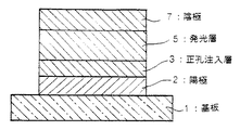
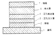
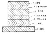
図1〜3は本発明の有機電界発光素子の実施の形態を示す模式的な断面図であり、1は基板、2は陽極、3は正孔注入層、4は正孔輸送層、5は発光層、6は電子輸送層、7は陰極を各々表わす。
【0030】
基板1は有機電界発光素子の支持体となるものであり、石英やガラスの板、金属板や金属箔、プラスチックフィルムやシートなどが用いられる。特にガラス板や、ポリエステル、ポリメタクリレート、ポリカーボネート、ポリスルホンなどの透明な合成樹脂の板が好ましい。合成樹脂基板を使用する場合にはガスバリア性に留意する必要がある。基板のガスバリヤ性が低すぎると、基板を通過する外気により有機電界発光素子が劣化することがあるので好ましくない。このため、合成樹脂基板のどちらか片側もしくは両側に緻密なシリコン酸化膜等を設けてガスバリア性を確保する方法も好ましい方法の一つである。
【0031】
基板1上には陽極2が設けられる。陽極2は正孔注入層3への正孔注入の役割を果たすものである。この陽極2は、通常、アルミニウム、金、銀、ニッケル、パラジウム、白金等の金属、インジウム及び/またはスズの酸化物などの金属酸化物、ヨウ化銅などのハロゲン化金属、カーボンブラック等により構成される。陽極2の形成は通常、スパッタリング法、真空蒸着法などにより行われることが多い。また、銀などの金属微粒子、ヨウ化銅などの微粒子、カーボンブラック、導電性の金属酸化物微粒子等を適当なバインダー樹脂溶液に分散し、基板1上に塗布することにより陽極2を形成することもできる。陽極2は異なる物質で積層して形成することも可能である。陽極2の厚みは、必要とする透明性により異なる。透明性が必要とされる場合は、可視光の透過率を、通常60%以上、好ましくは80%以上とすることが望ましく、この場合、厚みは、通常10〜1000nm、好ましくは20〜500nm程度である。不透明でよい場合は陽極2は基板1と同一でもよい。また、上記の陽極2の上に異なる導電材料を積層することも可能である。
【0032】
図1〜3に示す素子構造においては、陽極2の上に正孔注入層3が設けられる。この正孔注入層3に用いられる材料に要求される条件としては、陽極2からの正孔注入効率が高く、かつ、注入された正孔を効率よく輸送することができる材料であることが挙げられる。そのためには、イオン化ポテンシャルが小さく、可視光の光に対して透明性が高く、しかも正孔移動度が大きく、さらに安定性に優れ、トラップとなる不純物が製造時や使用時に発生しにくいことが要求される。
【0033】
本発明の有機電界発光素子は、好ましくはこの正孔注入層3を、分子量1,000未満の正孔輸送材料と該正孔輸送材料を酸化しうる電子受容性化合物を含有する層とする。また、本発明においては、この正孔注入層3を湿式製膜法で陽極2上に形成することにより、素子の駆動電圧を下げるとともに、陽極2のITO表面を平坦化し、電極間の短絡を防止し、更には正孔注入層3の構成材料の選択の幅を広げるといった効果を得る。
【0034】
この正孔注入層3に用いる正孔輸送材料としては、0.01cm2/V・秒以上の正孔移動度を有する材料であれば使用可能である。この目的に適う材料として、芳香族アミン化合物が挙げられる。例えば、4,4'-ビス[N-(1-ナフチル)-N-フェニルアミノ]ビフェニルで代表される2個以上の3級アミンを含み2個以上の縮合芳香族環が窒素原子に置換した芳香族ジアミン(特開平5−234681号公報)、4,4',4"-トリス(1-ナフチルフェニルアミノ)トリフェニルアミン等のスターバースト構造を有する芳香族アミン化合物(J.Lumin.,72-74巻、985頁、1997年)、トリフェニルアミンの四量体から成る芳香族アミン化合物(Chem.Commun.,2175頁、1996年)、2,2',7,7'-テトラキス-(ジフェニルアミノ)-9,9'-スピロビフルオレン等のスピロ化合物(Synth.Metals,91巻、209頁、1997年)等が挙げられる。これらの化合物は、単独で用いてもよいし、必要に応じて2種以上を混合して用いてもよい。
【0035】
正孔輸送材料としては、フタロシアニン誘導体又はポルフィリン誘導体も用いることができる。これらの化合物の好ましい具体例としては、以下の化合物が挙げられる。
【0036】
ポルフィン
5,10,15,20-テトラフェニル-21H,23H-ポルフィン
5,10,15,20-テトラフェニル-21H,23H-ポルフィンコバルト(II)
5,10,15,20-テトラフェニル-21H,23H-ポルフィン銅(II)
5,10,15,20-テトラフェニル-21H,23H-ポルフィン亜鉛(II)
5,10,15,20-テトラフェニル-21H,23H-ポルフィンバナジウム(IV)オキシド
5,10,15,20-テトラ(4-ピリジル)-21H,23H-ポルフィン
29H,31H-フタロシアニン
銅(II)フタロシアニン
亜鉛(II)フタロシアニン
チタンフタロシアニンオキシド
マグネシウムフタロシアニン
鉛フタロシアニン
銅(II)4,4',4'',4'''-テトラアザ-29H,31H-フタロシアニン
【0037】
また、正孔輸送材料としては、ジアリールアミノ基を有する8−ヒドロキシキノリン誘導体の金属錯体を用いることもでき、例えば、下記一般式(I)で表されるものが挙げられる。
【0038】
【化3】
((I)式中、Ar1及びAr2は、各々独立して置換基を有していてもよい芳香族基または芳香族複素環基を示し、R1〜R5は、それぞれ独立して、水素原子、ハロゲン原子、アルキル基、アラルキル基、アルケニル基、アルキニル基、シアノ基、アミノ基、アミド基、ニトロ基、アシル基、アルコキシカルボニル基、カルボキシル基、アルコキシ基、アルキルスルホニル基、水酸基、芳香族炭化水素基または芳香族複素環基を表す。なお、R1とR2、R2とR3、或いはR4とR5とは環を形成していてもよく、また、R1〜R5のいずれかがアルキル基、アラルキル基、アルケニル基、アルキニル基、2級若しくは3級アミノ基、アミド基、アシル基、アルコキシカルボニル基、アルコキシ基、アルキルスルホニル基、芳香族炭化水素基または芳香族複素環基を表す場合には、このものは更にその炭化水素部分に置換基を有していてもよい。Mは、アルカリ金属、アルカリ土類金属、Sc,Y,V,Cr,Mn,Fe,Co,Ni,Cu,Zn,Cd、Al、Ga,In,Si,Ge,Sn,Sm、EuまたはTbを表し、nは2から4までの整数を示す。)
【0040】
上記一般式(I)で表される化合物の具体例としては、次のようなものが挙げられる。
【0041】
【化4】
その他、α−セキシチオフェン等のオリゴチオフェン誘導体も、好ましい正孔輸送材料の例として挙げられる。
【0043】
なお、このような正孔輸送材料の分子量が1,000以上であると、低分子化合物を用いることによる正孔移動度の向上効果が得られないため、本発明において、正孔輸送材料としては分子量1,000未満、好ましくは400〜800のものを用いる。
【0044】
正孔注入層3を形成する上記正孔輸送材料と混合して用いられる、正孔輸送材料を酸化して正孔注入層の導電率を向上させる電子受容性化合物としては、酸化剤が好ましく用いられ、特にハロゲン化金属、ルイス酸、有機酸、アリールアミンとハロゲン化金属又はルイス酸との塩が好適である。
【0045】
このような電子受容性化合物の具体例としては、以下に示す化合物が挙げられる。
【0046】
【化5】
なお、正孔注入層3中の電子受容性化合物の前記正孔輸送材料に対する含有量は、通常0.1〜50モル%、特に1〜30モル%の範囲にあることが好ましい。
【0048】
本発明において、前記正孔輸送材料と電子受容性化合物とを含有する正孔注入層3は湿式製膜法により前記陽極2上に形成される。例えば、前記正孔輸送材料と電子受容性化合物の所定量に、必要により正孔のトラップにならないバインダー樹脂や塗布性改良剤などの添加剤等を添加し、溶解して塗布溶液を調製し、スピンコート法やディップコート法などの湿式製膜法により陽極2上に塗布し、乾燥して正孔注入層3を形成する。
【0049】
なお、バインダー樹脂を含有する場合、その種類や含有量によっては、該層における正孔移動度が低下する畏れがある。よって正孔移動度の面からは、バインダー樹脂の含有量は、該層中50重量%以下が好ましく、30重量%以下がより好ましく、実質的にバインダー樹脂を含有しない場合が最も好ましい。
【0050】
本発明における、前記正孔輸送材料と電子輸送性化合物を含む層は、上述の如く、湿式製膜及び乾燥工程のみで形成することも可能であるが、更に加熱工程を経ることにより、得られる膜に含まれる分子のマイグレーションを活性化し、熱的に安定な薄膜構造に到達させることができ、これにより膜の表面平坦性が向上し、かつ素子の発光効率が向上するため好ましい。
【0051】
具体的には、前記正孔輸送材料と電子受容性化合物を含む層を湿式製膜法にて形成した後、用いた正孔輸送材料のガラス転移点Tg以下の温度で加熱する。この加熱温度は、正孔輸送材料のガラス転移点Tgより10℃以上低温であることが好ましい。また、加熱処理による効果を十分に得るためには、60℃以上で処理する。加熱時間は通常1分〜8時間程度である。
【0052】
前述の如く、従来の有機電界発光素子では、ITO等の陽極2の表面粗さに起因する素子作製時の短絡の問題があったが、このように湿式製膜法により形成された正孔注入層は、表面が平滑なものとなるため、この短絡の問題を解消することができる。
【0053】
このようにして形成される正孔注入層3の膜厚は、通常5〜1000nm、好ましくは10〜500nmである。
【0054】
正孔注入層3の上には発光層5が設けられる。発光層5は、電界を与えられた電極間において陰極7から注入された電子と正孔注入層3から輸送された正孔を効率よく再結合し、かつ、再結合により効率よく発光する材料から形成される。
【0055】
このような条件を満たす材料としては、8−ヒドロキシキノリンのアルミニウム錯体などの金属錯体(特開昭59−194393号公報)、10-ヒドロキシベンゾ[h]キノリンの金属錯体(特開平6−322362号公報)、ビススチリルベンゼン誘導体(特開平1−245087号公報、同2−222484号公報)、ビススチリルアリーレン誘導体(特開平2−247278号公報)、(2-ヒドロキシフェニル)ベンゾチアゾールの金属錯体(特開平8−315983号公報)、シロール誘導体等が挙げられる。これらの発光層材料は、通常は真空蒸着法により正孔注入層3上に積層形成される。
【0056】
素子の発光効率を向上させるとともに発光色を変える目的で、例えば、8−ヒドロキシキノリンのアルミニウム錯体をホスト材料として、クマリン等のレーザ用蛍光色素をドープすること(J.Appl.Phys.,65巻,3610頁,1989年)等が行われている。この方法の利点は、
1)高効率の蛍光色素により発光効率が向上、
2)蛍光色素の選択により発光波長が可変、
3)濃度消光を起こす蛍光色素も使用可能、
4)薄膜性のわるい蛍光色素も使用可能、
等が挙げられる。
【0057】
素子の駆動寿命を改善する目的においても、前記発光層材料をホスト材料として、蛍光色素をドープすることは有効である。例えば、8−ヒドロキシキノリンのアルミニウム錯体などの金属錯体をホスト材料として、ルブレンに代表されるナフタセン誘導体(特開平4−335087号公報)、キナクリドン誘導体(特開平5−70773号公報)、ペリレン等の縮合多環芳香族環(特開平5−198377号公報)を、ホスト材料に対して0.1〜10重量%ドープすることにより、素子の発光特性、特に駆動安定性を大きく向上させることができる。発光層のホスト材料に上記ナフタセン誘導体、キナクリドン誘導体、ペリレン等の蛍光色素をドープする方法としては、共蒸着による方法と蒸着源を予め所定の濃度で混合しておく方法がある。
【0058】
高分子系の発光層材料としては、先に挙げたポリ(p-フェニレンビニレン)、ポリ[2-メトキシ-5-(2-エチルヘキシルオキシ)-1,4-フェニレンビニレン]、ポリ(3-アルキルチオフェン)等の高分子材料や、ポリビニルカルバゾール等の高分子に発光材料と電子移動材料を混合した系等が挙げられる。これらの材料は正孔注入層と同様にスピンコートやディップコート等の方法により正孔注入層3上に塗布して薄膜形成される。
【0059】
このようにして形成される発光層5の膜厚は、通常10〜200nm、好ましくは30〜100nmである。
【0060】
素子の発光特性を向上させるために、図2に示すように、正孔輸送層4を正孔注入層3と発光層5との間に設けたり、さらには、図3に示す様に電子輸送層6を発光層5と陰極7との間に設けるなど機能分離型にすることが行われる。
【0061】
図2及び図3の機能分離型素子において、正孔輸送層4の材料としては、正孔注入層3からの正孔注入効率が高く、かつ、注入された正孔を効率よく輸送することができる材料であることが必要である。そのためには、イオン化ポテンシャルが小さく、しかも正孔移動度が大きく、さらに安定性に優れ、トラップとなる不純物が製造時や使用時に発生しにくいことが要求される。また、発光層と直接接する層であるために、発光を消光する物質が含まれていないことが望ましい。
【0062】
このような正孔輸送材料としては、すでに、正孔注入層を形成する正孔輸送材料として挙げた、4,4'-ビス[N-(1-ナフチル)-N-フェニルアミノ]ビフェニルで代表される2個以上の3級アミンを含み2個以上の縮合芳香族環が窒素原子に置換した芳香族ジアミン(特開平5−234681号公報)、4,4',4"-トリス(1-ナフチルフェニルアミノ)トリフェニルアミン等のスターバースト構造を有する芳香族アミン化合物(J.Lumin.,72-74巻、985頁、1997年)、トリフェニルアミンの四量体から成る芳香族アミン化合物(Chem.Commun.,2175頁、1996年)、2,2',7,7'-テトラキス-(ジフェニルアミノ)-9,9'-スピロビフルオレン等のスピロ化合物(Synth.Metals,91巻、209頁、1997年)等が挙げられる。これらの化合物は、単独で用いてもよいし、必要に応じて、2種以上を混合して用いてもよい。
【0063】
上記の化合物以外に、正孔輸送層4の材料として、ポリビニルカルバゾール、ポリビニルトリフェニルアミン(特開平7−53953号公報)、テトラフェニルベンジジンを含有するポリアリーレンエーテルサルホン(Polym.Adv.Tech.,7巻、33頁、1996年)等の高分子材料が挙げられる。
【0064】
正孔輸送層4は上記の正孔輸送材料を塗布法あるいは真空蒸着法により前記正孔注入層3上に積層することにより形成される。
【0065】
塗布法の場合は、正孔輸送材料の1種または2種以上に、必要により正孔のトラップにならないバインダー樹脂や塗布性改良剤などの添加剤とを添加し、溶解して塗布溶液を調製し、スピンコート法などの方法により正孔注入層3上に塗布し、乾燥して正孔輸送層4を形成する。ここで、バインダー樹脂としては、ポリカーボネート、ポリアリレート、ポリエステル等が挙げられる。バインダー樹脂は添加量が多いと正孔移動度を低下させるので、少ない方が望ましく、通常50重量%以下が好ましい。
【0066】
真空蒸着法の場合には、正孔輸送材料を真空容器内に設置されたルツボに入れ、真空容器内を適当な真空ポンプで10−4Pa程度にまで排気した後、ルツボを加熱して、正孔輸送材料を蒸発させ、ルツボと向き合って置かれた、陽極2および正孔注入層3が形成された基板1上に正孔輸送層4を形成する。
【0067】
このようにして形成される正孔輸送層4の膜厚は、通常10〜300nm、好ましくは30〜100nmである。このように薄い膜を一様に形成するためには、一般に真空蒸着法がよく用いられる。
【0068】
また、電子輸送層6に用いられる化合物には、陰極からの電子注入が容易で、電子の輸送能力がさらに大きいことが要求される。このような電子輸送材料としては、既に発光層材料として挙げた8−ヒドロキシキノリンのアルミニウム錯体、オキサジアゾール誘導体(Appl.Phys.Lett.,55巻,1489頁,1989年)やそれらをポリメタクリル酸メチル(PMMA)等の樹脂に分散した系、フェナントロリン誘導体(特開平5−331459号公報)、2-t-ブチル-9,10-N,N'-ジシアノアントラキノンジイミン、n型水素化非晶質炭化シリコン、n型硫化亜鉛、n型セレン化亜鉛等が挙げられる。電子輸送層6の膜厚は、通常5〜200nm、好ましくは10〜100nmである。
【0069】
陰極7は、発光層5に電子を注入する役割を果たす。陰極7として用いられる材料は、前記陽極2に使用される材料を用いることが可能であるが、効率よく電子注入を行なうには、仕事関数の低い金属が好ましく、スズ、マグネシウム、インジウム、カルシウム、アルミニウム、銀等の適当な金属またはそれらの合金が用いられる。具体例としては、マグネシウム−銀合金、マグネシウム−インジウム合金、アルミニウム−リチウム合金等の低仕事関数合金電極が挙げられる。
【0070】
陰極7の膜厚は通常、陽極2と同様である。低仕事関数金属から成る陰極を保護する目的で、この上にさらに、仕事関数が高く大気に対して安定な金属層を積層することは素子の安定性を増す上で有効である。この目的のために、アルミニウム、銀、銅、ニッケル、クロム、金、白金等の金属が使われる。
【0071】
さらに、陰極7と発光層5または電子輸送層6の界面にLiF、MgF2、Li2O等の極薄絶縁膜(膜厚0.1〜5nm)を挿入することも、素子の効率を向上させる有効な方法である(Appl.Phys.Lett.,70巻,152頁,1997年;特開平10−74586号公報;IEEE Trans.Electron.Devices,44巻,1245頁,1997年)。
【0072】
図1〜3は、本発明で採用される素子構造の一例であって、本発明は何ら図示のものに限定されるものではない。例えば、図1とは逆の構造、即ち、基板1上に陰極7、発光層5、正孔注入層3、陽極2の順に積層することも可能であり、既述したように少なくとも一方が透明性の高い2枚の基板の間に本発明の有機電界発光素子を設けることも可能である。同様に、図2及び図3に示したものについても、前記各構成層を逆の構造に積層することも可能である。また、各層間に前述の層以外の任意の層が形成されていても良い。
【0073】
なお、図1〜3においては、前記正孔輸送材料と電子受容性化合物を含有する層を、陽極に接する正孔注入層として設けてあるが、本発明においては、この層は必ずしも正孔注入層である必要はなく、陽極と発光層との間に設けられていれば良い。ただし、この湿式製膜法で形成される層を正孔注入層として陽極に接して設けることにより、陽極の表面粗さに起因する素子の短絡の問題を解消することができ、また、耐熱性の高い層を陽極に接して設けることで高温下での安定性も高められ、好ましい。
【0074】
【実施例】
次に、実験例、製造例、実施例及び比較例によって本発明を更に具体的に説明するが、本発明はその要旨を超えない限り、以下の実施例の記載に限定されるものではない。
【0075】
実験例1
ITOガラス基板を、アセトンで超音波洗浄、純水で水洗、イソプロピルアルコールで超音波洗浄、乾燥窒素で乾燥、UV/オゾン洗浄を行った後、正孔輸送材料として以下に示す芳香族アミン化合物:4,4'-ビス[N-(m-トリル)-N-フェニルアミノ]ビフェニルと、電子受容性化合物としてSbCl5を20モル%(前記芳香族アミン化合物に対して)含有する1,2-ジクロロメタン溶液(芳香族アミン化合物の濃度5mM)を、上記ITOガラス基板上にスピンコート(スピナ回転数1,000rpm;スピナ回転時間40秒)した。その後、真空中で室温にて1時間乾燥して、15nmの膜厚の均一な薄膜を得た。
【0076】
【化6】
この試料の平均表面粗さ(Ra)をAFM(原子間力顕微鏡;セイコーインスツルメンツ社製SPA300HV/SPI3800N)により測定したところ、1nmと非常に平滑であった。一方、膜を形成しないITOガラス基板のRaは7.5nmであった。
【0078】
この結果から、有機膜を塗布法により湿式製膜することで、ITOガラス基板の平坦化効果が得られることが確認された。
【0079】
製造例1
図3に示す構造を有する有機電界発光素子を以下の方法で作製した。
【0080】
ガラス基板上にインジウム・スズ酸化物(ITO)透明導電膜120nm堆積したもの(ジオマテック社製;電子ビーム成膜品;シート抵抗15Ω)を通常のフォトリソグラフィ技術と塩酸エッチングを用いて3mm幅のストライプにパターニングして陽極2を形成した。パターン形成したITO基板を、アセトンによる超音波洗浄、純水による水洗、イソプロピルアルコールによる超音波洗浄の順で洗浄後、窒素ブローで乾燥させ、最後に紫外線オゾン洗浄を行った。
【0081】
このITOガラス基板上に、実験例1と同一条件で4,4'-ビス[N-(m-トリル)-N-フェニルアミノ]ビフェニルとSbCl5をスピンコートし、15nmの膜厚の均一な薄膜形状を有する正孔注入層3を形成した。
【0082】
次に、上記正孔注入層3を塗布成膜した基板1を真空蒸着装置内に設置した。上記装置の粗排気を油回転ポンプにより行った後、装置内の真空度が2×10⁻⁶Torr(約2.7×10⁻⁴Pa)以下になるまで液体窒素トラップを備えた油拡散ポンプを用いて排気した。上記装置内に配置されたタンタルボードに入れた芳香族アミン化合物:4,4'-ビス[N-(m-トリル)-N-フェニルアミノ]ビフェニルを、タンタルボートに通電加熱して蒸着を行った。蒸着時の真空度は3×10⁻⁶Torr(約4×10⁻⁴Pa)、蒸着速度は0.2nm/秒で、膜厚75nmの膜を正孔注入層3の上に積層して正孔輸送層4を完成させた。
【0083】
引続き、発光層5の材料として、以下の構造式に示すアルミニウムの8−ヒドロキシキノリン錯体、Al(C9H6NO)3、を正孔輸送層4と同様にして蒸着を行った。この時のアルミニウムの8−ヒドロキシキノリン錯体の蒸着速度は0.25nm/秒で、蒸着時の真空度は3×10−6Torr(約4×10−4Pa)、蒸着された発光層5の膜厚は75nmであった。
【0084】
【化7】
さらに、陰極からの電子注入を容易にするために、電子輸送層6として安息香酸のリチウム塩を、蒸着速度0.5nm/秒、蒸着時の真空度3×10−6Torr(約4×10−4Pa)の条件において、膜厚2nmで形成した。
【0086】
上記の正孔輸送層4、発光層5及び電子輸送層6を真空蒸着する時の基板温度は室温に保持した。
【0087】
ここで、電子輸送層6までの蒸着を行った素子に、陰極蒸着用のマスクとして3mm幅のストライプ状シャドーマスクを、陽極2のITOストライプとは直交するように素子に密着させた。このマスク交換作業は真空をやぶらずに行った。
【0088】
続いて、陰極7として、アルミニウムを蒸着速度1nm/秒で電子輸送層6上に膜厚90nmで形成した。蒸着時の真空度は6.0×10−5Torr(約8×10−4Pa)であった。陰極蒸着時の基板温度は室温に保持した。
【0089】
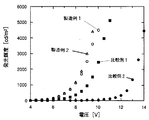
以上の様にして、3mm×3mmのサイズの有機電界発光素子が得られた。この素子を陰極蒸着装置から取り出した後、大気中において陽極と陰極間に順方向の電圧を印加して発光特性を測定した。この素子の輝度−電圧特性を図4のグラフに示す。図4より明らかなように、この素子が輝度100cd/m2に達する電圧は5.6Vと低電圧であった。
【0090】
製造例2
正孔注入層を形成する正孔輸送材料として以下の構造式に示す芳香族アミン化合物:4,4'-ビス[N-(1-ナフチル)-N-フェニルアミノ]ビフェニルを用いた他は、製造例1と同様にして素子を作製し、得られた素子の輝度−電圧特性を調べ、結果を図4に示した。図4より明らかなように、この素子が輝度100cd/m2に達する電圧は5.6Vと低電圧であった。
【0091】
【化8】
実験例2
実験例1と同様にして洗浄したITO基板上に、正孔輸送材料として下記に示す芳香族アミン化合物を用い、電子受容性化合物としてTBPAH(トリス(4−ブロモフェニル)アミニウムヘキサクロロアンチモネート)を用いた他は、実験例1と同様にして塗布、乾燥を行って、正孔輸送材料と電子受容性化合物とを含む薄膜を膜厚25nmで形成した。用いた正孔輸送材料のガラス転移温度Tgは146℃であった。
【0093】
【化9】
この膜を窒素雰囲気中、115℃で60分加熱処理したものと、加熱処理しないものとについて、その表面粗さをAFMで測定し、結果を表1に示した。表1より、加熱処理により、膜表面の平坦化効果が得られることがわかる。
【0095】
【表1】
実施例1,比較例3
実験例2と同様にして正孔注入層を形成した他は、製造例1と同様にして素子を作製した。
【0097】
即ち、比較例3では、正孔注入層の形成に当たり、湿式製膜後加熱処理を行わずに実験例2と同様に行い、その他は製造例1と同様にして素子を作製した。また、実施例1では、正孔注入層の形成に当たり、湿式製膜後加熱処理を行って実験例2と同様に行い、その他は製造例1と同様にして素子を作製した。
【0098】
各素子の発光特性を表2に示す。表2より、湿式製膜後の加熱処理により、発光効率が改善されることがわかる。
【0099】
【表2】
比較例1
正孔注入層として膜厚15nmの銅フタロシアニン層を用いた他は、製造例1と同様にして素子を作製し、得られた素子の輝度−電圧特性を調べ、図4に示した。図4より明らかなように、この素子が輝度100cd/m2に達する電圧は7.0Vと製造例1,2に比べて高かった。
【0101】
比較例2
正孔注入層を設けない他は、製造例1と同様にして素子を作製し、得られた素子の輝度−電圧特性を調べ、結果を図4に示した。図4より明らかなように、この素子が輝度100cd/m2に達する電圧は11.0Vと高電圧であった。
【0102】
【発明の効果】
以上詳述した通り、陽極と陰極との間に、低分子の正孔輸送材料と電子受容性化合物とを含有する層を湿式製膜法により形成した本発明の有機電界発光素子によれば、低電圧での高発光効率駆動が可能で、しかも耐熱性が良好な素子が提供される。
【0104】
従って、本発明による有機電界発光素子は、フラットパネル・ディスプレイ(例えばOAコンピュータ用や壁掛けテレビ)や面発光体としての特徴を生かした光源(例えば、複写機の光源、液晶ディスプレイや計器類のバックライト光源)、表示板、標識灯への応用が考えられ、特に、高耐熱性が要求される車載用表示素子として、その技術的価値は大きいものである。
【図面の簡単な説明】
【図1】 本発明の有機電界発光素子の実施の形態の一例を示す模式的な断面図である。
【図2】 本発明の有機電界発光素子の実施の形態の他の例を示す模式的な断面図である。
【図3】 本発明の有機電界発光素子の実施の形態の別の例を示す模式的な断面図である。
【図4】 製造例1,2及び比較例1,2で作製した素子の輝度−電圧特性を示すグラフである。
【符号の説明】
1 基板
2 陽極
3 正孔注入層
4 正孔輸送層
5 発光層
6 電子輸送層
7 陰極[0001]
BACKGROUND OF THE INVENTION
The present invention relates to a method of fabricating an organic light emitting element, and more particularly to a method of manufacturing a thin film type device that emits light by applying an electric field to the light-emitting layer comprising an organic compound.
[0002]
[Prior art]
Conventionally, as a thin film type electroluminescent (EL) element, there are ZnS, CaS, SrS, etc. which are inorganic material II-VI compound semiconductors, Mn which is an emission center, rare earth elements (Eu, Ce, Tb, Sm, etc.) ) Is generally used, but an EL element made from the above inorganic material is
1) AC drive is required (generally 50-1000Hz),
2) High drive voltage (generally around 200V)
3) Full color is difficult, especially blue
4) The cost of the peripheral drive circuit is high.
Has the problem.
[0003]
However, in recent years, EL devices using organic thin films have been developed to improve the above problems. In particular, in order to improve luminous efficiency, the type of electrode is optimized for the purpose of improving the efficiency of carrier injection from the electrode, and a hole transporting layer made of aromatic diamine and a light emitting layer made of 8-hydroxyquinoline aluminum complex, Development of an organic electroluminescent device equipped with a light emitting diode (Appl. Phys. Lett., 51, 913, 1987) significantly improves luminous efficiency compared to conventional EL devices using single crystals such as anthracene. Has been made and practical characteristics are approaching.
[0004]
In addition to the electroluminescent device using the low molecular weight material as described above, as a material of the light emitting layer, poly (p-phenylene vinylene), poly [2-methoxy-5- (2-ethylhexyloxy) -1,4 -Phenylene vinylene], poly (3-alkylthiophene), and other electroluminescent devices using polymer materials such as polyfluorene, and low molecular light emitting materials and electron transfer materials mixed and dispersed in polymers such as polyvinylcarbazole Devices are also being developed.
[0005]
By the way, the biggest problem of the organic electroluminescence device is the lifetime at the time of driving, and as development of instability at the time of driving, the emission luminance decreases, the voltage increases at constant current driving, the non-light emitting portion (dark spot) Generation and the like. Although there are several causes of these instabilities, the deterioration of the thin film shape of the organic layer is dominant. It is considered that the deterioration of the thin film shape is caused by crystallization (or aggregation) of the organic amorphous film due to heat generated when the element is driven. In particular, contact between the anode and the hole transport layer is important for increasing the drive voltage.
[0006]
Therefore, in order to improve the contact between the anode and the hole transport layer, it has been studied to provide a hole injection layer between the two layers to lower the driving voltage. The conditions required for the material used for the hole injection layer include good contact with the anode, formation of a uniform thin film, and thermal stability, that is, a high melting point and glass transition temperature Tg, preferably It is required to have a melting point of 300 ° C or higher and a Tg of 100 ° C or higher. Furthermore, the ionization potential is low, hole injection from the anode is easy, and the hole mobility is high.
[0007]
Conventionally, various materials for the hole injection layer have been studied. For example, porphyrin derivatives, phthalocyanine compounds (Japanese Patent Laid-Open No. 63-295695), star bust type aromatic triamine (Japanese Patent Laid-Open No. 4-308688). ), Hydrazone compounds (JP-A-4-320483), organic compounds such as polythienylene vinylene, polythiophene and polyaniline, sputtered carbon films, metal oxides such as vanadium oxide, ruthenium oxide and molybdenum oxide Etc. have been reported.
[0008]
[Problems to be solved by the invention]
However, in the method of inserting a hole injection layer between the anode and the hole transport layer, when a porphyrin derivative or a phthalocyanine compound is used as the hole injection layer, the spectrum changes due to light absorption by these films themselves. Or is colored in appearance and is not transparent.
[0009]
Starbust aromatic triamines have the advantage of low ionization potential and good transparency, but have low heat resistance due to their low glass transition point and low melting point.
[0010]
Conjugated polymers such as polythienylene vinylene, polythiophene, and polyaniline have a problem in solubility and a problem in process.
[0011]
Further, a non-conjugated polymer not mixed with an electron-accepting compound is used for the hole transport layer (Japanese Patent Laid-Open Nos. 9-188756 and 11-135262). As described in JP-A-9-188756, page 17, FIG. 4, the efficiency is as high as 20 cd / m 2 at 6 V, and the luminous efficiency at that time is as low as 1 cd / A.
[0012]
Furthermore, although it is disclosed that low voltage driving is possible by mixing an electron accepting compound with a non-conjugated hole transporting polymer (Japanese Patent Laid-Open No. 11-283750), the polymer disclosed here Is considered to have a low glass transition temperature Tg, and there is no description that heat resistance has been improved.
[0013]
Thus, the high voltage at the time of driving the organic electroluminescent element and the low stability including heat resistance are a big problem as a light source for a backlight of a facsimile, a copying machine, a liquid crystal display, Particularly, it is not desirable as a display element such as a full color flat panel display.
[0014]
In addition, in a conventional organic electroluminescence device, indium tin oxide (ITO), which is usually used as an anode, has a surface roughness of about 10 nm (Ra), and in addition, locally has protrusions. In many cases, it has a problem that a short-circuit defect is produced during device fabrication.
[0015]
A hole injection layer using a polymer is preferable because it has high flatness on the surface of the layer and covers the flatness of ITO, but a low molecular weight compound is generally preferable from the viewpoint of high hole mobility.
[0016]
Japanese Patent Application Laid-Open No. 11-251067 discloses that a hole injection layer made of a hole transport material and an electron accepting compound is formed by a vacuum deposition method. However, in forming the hole injection layer, if the vacuum deposition method is used, the electron-accepting compound is thermally decomposed and the inside of the vacuum deposition apparatus is corroded, so that the selection range of the material is limited.
[0017]
The present invention solves the above-mentioned conventional problems, can be driven with low voltage and high luminous efficiency, has good heat resistance, and maintains stable luminous characteristics over a long period of time at high temperatures. An object of the present invention is to provide an organic electroluminescent device that can be used.
[0018]
Another object of the present invention is to provide an organic electroluminescence device capable of preventing short-circuit defects during device fabrication due to the surface roughness of the anode and further widening the selection range of materials used. And
[0019]
[Means for Solving the Problems]
Method of fabricating an organic light emitting device of the present invention, on a substrate, have a light-emitting layer which is sandwiched by the anode and the cathode, between the anode and emitting layer, a hole transport material having a molecular weight less than 1,000 A method for producing an organic electroluminescent device in which a layer containing an electron-accepting compound capable of oxidizing the hole-transporting material is formed by a wet film-forming method, the hole-transporting material and the electron-accepting compound And a step of heating at a temperature not lower than 60 ° C. and not higher than the glass transition point of the hole transporting material after forming the layer including the film by a wet film forming method .
[0020]
That is, the present inventors have intensively studied to solve the conventional problems and provide an organic electroluminescence device capable of maintaining stable light emission characteristics at a high temperature. As a result, the light emission sandwiched between the anode and the cathode on the substrate. In an organic electroluminescent device having a layer, a layer containing a hole transport material having a molecular weight of less than 1,000 and an electron-accepting compound capable of oxidizing the hole transport material is formed between the anode and the light-emitting layer by wet film formation. It has been found that the above problems can be solved by the method, preferably by providing as a hole injection layer in contact with the anode, and the present invention has been completed.
[0021]
In the present invention, by using a hole transport material and an electron-accepting compound capable of oxidizing the mixture, it is possible to simultaneously improve the light emitting characteristics and heat resistance of the device. That is, when an electron-accepting compound is mixed with an electron-donating hole transport material, charge transfer occurs, and as a result, holes that are free carriers are generated, and the electrical conductivity of this layer increases. By providing such a layer, the electrical connection between the light emitting layer and the anode is improved, the driving voltage is lowered, and the stability during continuous driving is also improved. In addition, in the present invention, since a hole transport material having a molecular weight of less than 1,000 is used, the hole mobility is high.
[0022]
In general, in the case of forming a layer using a low molecular compound in an organic electroluminescent device, a vacuum deposition method is usually used, but according to the present invention, a hole transport material having a molecular weight of less than 1,000, an electron accepting compound, and By forming a layer containing, by a wet film forming method,
・ A wider range of materials can be used. Therefore, a material having a high Tg can be selected from a wide range, and the heat resistance of the element can be improved.
-A layer with high surface flatness can be obtained. For this reason, by forming such a layer on the anode, the surface roughness of the anode described above is relaxed, a good surface smoothing effect is obtained, and short circuit defects during device fabrication are prevented.
An excellent effect is achieved.
[0023]
In the layer containing a hole transport material having a molecular weight of less than 1,000 according to the present invention and an electroceptive compound capable of oxidizing the same, the binder resin content is preferably 50% by weight or less. In addition, this layer is a layer exhibiting a hole transport property, and may be anywhere between the anode and the light emitting layer. As shown in FIGS. Although it is not limited at all, in order to make full use of the advantages of this layer that the electrical connection with the anode (inorganic material) is good and the heat resistance can be enhanced, it is formed as a hole injection layer at a position in contact with the anode. Is most advantageous.
[0024]
In the present invention, as the hole transport material, for example,
Aromatic amine compounds Phthalocyanine derivatives or porphyrin derivatives Metal complexes of 8-hydroxyquinoline derivatives having a diarylamino group include oligothiophene derivatives.
[0025]
The electron-accepting compound that can oxidize the hole transport material includes a metal halide, a Lewis acid, an organic acid, a salt of an arylamine and a metal halide, and a group of an arylamine and a Lewis acid. 1 type or 2 types or more selected from 1 type, Preferably 1 type or 2 types or more selected from the following compound group is mentioned.
[0026]
[Chemical 2]
By passing through the heating step as in the method for producing an organic electroluminescent element of the present invention, the migration of molecules contained in the obtained film can be activated, and a thermally stable thin film structure can be reached. The surface flatness can be improved and the light emission efficiency of the device can be improved.
[0028]
DETAILED DESCRIPTION OF THE INVENTION
Hereinafter will be described with reference to embodiments of the method for manufacturing the organic electroluminescence element of the invention in detail to the drawings.
[0029]
1 to 3 are schematic cross-sectional views showing an embodiment of the organic electroluminescence device of the present invention, wherein 1 is a substrate, 2 is an anode, 3 is a hole injection layer, 4 is a hole transport layer, The light emitting layer, 6 represents an electron transport layer, and 7 represents a cathode.
[0030]
The substrate 1 serves as a support for the organic electroluminescent element, and a quartz or glass plate, a metal plate or a metal foil, a plastic film, a sheet, or the like is used. In particular, a glass plate or a transparent synthetic resin plate such as polyester, polymethacrylate, polycarbonate, or polysulfone is preferable. When using a synthetic resin substrate, it is necessary to pay attention to gas barrier properties. If the gas barrier property of the substrate is too low, the organic electroluminescent element may be deteriorated by the outside air passing through the substrate, which is not preferable. For this reason, a method of providing a gas barrier property by providing a dense silicon oxide film or the like on one side or both sides of the synthetic resin substrate is also a preferable method.
[0031]
An anode 2 is provided on the substrate 1. The anode 2 plays a role of hole injection into the hole injection layer 3. The anode 2 is usually composed of a metal such as aluminum, gold, silver, nickel, palladium, or platinum, a metal oxide such as an oxide of indium and / or tin, a metal halide such as copper iodide, or carbon black. Is done. In general, the anode 2 is often formed by sputtering, vacuum deposition, or the like. Also, the anode 2 is formed by dispersing fine particles such as silver, fine particles such as copper iodide, carbon black, conductive metal oxide fine particles, etc. in an appropriate binder resin solution and applying the solution onto the substrate 1. You can also. The anode 2 can also be formed by stacking different materials. The thickness of the anode 2 varies depending on the required transparency. When transparency is required, the visible light transmittance is preferably 60% or more, preferably 80% or more. In this case, the thickness is usually 10 to 1000 nm, preferably about 20 to 500 nm. It is. If it may be opaque, the anode 2 may be the same as the substrate 1. It is also possible to laminate different conductive materials on the anode 2 described above.
[0032]
1 to 3, the hole injection layer 3 is provided on the anode 2. Conditions required for the material used for the hole injection layer 3 include a material having high hole injection efficiency from the anode 2 and capable of efficiently transporting the injected holes. It is done. For this purpose, the ionization potential is small, the transparency to visible light is high, the hole mobility is high, the stability is high, and impurities that become traps are less likely to be generated during manufacturing and use. Required.
[0033]
In the organic electroluminescent device of the present invention, the hole injection layer 3 is preferably a layer containing a hole transport material having a molecular weight of less than 1,000 and an electron accepting compound capable of oxidizing the hole transport material. In the present invention, the hole injection layer 3 is formed on the anode 2 by a wet film forming method, thereby lowering the driving voltage of the element, flattening the ITO surface of the anode 2 and shorting between the electrodes. In addition, the effect of widening the selection of the constituent material of the hole injection layer 3 can be obtained.
[0034]
As the hole transport material used for the hole injection layer 3, any material having a hole mobility of 0.01 cm 2 / V · sec or more can be used. A material suitable for this purpose includes an aromatic amine compound. For example, two or more condensed aromatic rings including two or more tertiary amines represented by 4,4′-bis [N- (1-naphthyl) -N-phenylamino] biphenyl are substituted with nitrogen atoms. Aromatic amine compounds having a starburst structure such as aromatic diamines (JP-A-5-234681), 4,4 ', 4 "-tris (1-naphthylphenylamino) triphenylamine (J. Lumin., 72 -74, 985, 1997), aromatic amine compounds consisting of tetraphenylamine tetramer (Chem. Commun., 2175, 1996), 2,2 ', 7,7'-tetrakis- ( Examples include spiro compounds such as diphenylamino) -9,9'-spirobifluorene (Synth. Metals, Vol. 91, p. 209, 1997), etc. These compounds may be used alone or as necessary. Two or more kinds may be mixed and used accordingly.
[0035]
As the hole transport material, a phthalocyanine derivative or a porphyrin derivative can also be used. Preferable specific examples of these compounds include the following compounds.
[0036]
Porphin
5,10,15,20-Tetraphenyl-21H, 23H-porphine
5,10,15,20-Tetraphenyl-21H, 23H-porphine cobalt (II)
5,10,15,20-Tetraphenyl-21H, 23H-porphine copper (II)
5,10,15,20-Tetraphenyl-21H, 23H-porphine zinc (II)
5,10,15,20-Tetraphenyl-21H, 23H-porphine vanadium (IV) oxide
5,10,15,20-Tetra (4-pyridyl) -21H, 23H-porphine
29H, 31H-phthalocyanine Copper (II) phthalocyanine Zinc (II) phthalocyanine Titanium phthalocyanine oxide Magnesium phthalocyanine Lead phthalocyanine Copper (II) 4,4 ', 4'',4'''-Tetraaza-29H, 31H-phthalocyanine
Moreover, as a hole transport material, the metal complex of the 8-hydroxyquinoline derivative which has a diarylamino group can also be used, For example, what is represented with the following general formula (I) is mentioned.
[0038]
[Chemical 3]
(In the formula (I), Ar 1 and Ar 2 each independently represents an aromatic group or an aromatic heterocyclic group which may have a substituent, and R 1 to R 5 each independently represents , Hydrogen atom, halogen atom, alkyl group, aralkyl group, alkenyl group, alkynyl group, cyano group, amino group, amide group, nitro group, acyl group, alkoxycarbonyl group, carboxyl group, alkoxy group, alkylsulfonyl group, hydroxyl group, represents an aromatic hydrocarbon group or an aromatic heterocyclic group. Incidentally, R 1 and R 2, R 2 and R 3, or R 4 and R 5 may form a ring, also, R 1 ~ either an alkyl group R 5, an aralkyl group, an alkenyl group, an alkynyl group, secondary or tertiary amino group, an amide group, an acyl group, an alkoxycarbonyl group, an alkoxy group, an alkylsulfonyl group, an aromatic hydrocarbon Motoma In the case where A represents an aromatic heterocyclic group, this may further have a substituent in the hydrocarbon portion, M is an alkali metal, an alkaline earth metal, Sc, Y, V, Cr, Mn, Fe, Co, Ni, Cu, Zn, Cd, Al, Ga, In, Si, Ge, Sn, Sm, Eu, or Tb is represented, and n represents an integer from 2 to 4.
[0040]
Specific examples of the compound represented by the general formula (I) include the following.
[0041]
[Formula 4]
In addition, oligothiophene derivatives such as α-sexithiophene are also examples of preferable hole transport materials.
[0043]
When the molecular weight of such a hole transport material is 1,000 or more, the effect of improving the hole mobility by using a low molecular compound cannot be obtained. Therefore, in the present invention, the molecular weight is 1,000 as the hole transport material. Less than that, preferably 400-800.
[0044]
An oxidant is preferably used as the electron-accepting compound that is used by mixing with the hole transport material forming the hole injection layer 3 and that improves the conductivity of the hole injection layer by oxidizing the hole transport material. Particularly preferred are metal halides, Lewis acids, organic acids, and salts of arylamines with metal halides or Lewis acids.
[0045]
Specific examples of such electron-accepting compounds include the following compounds.
[0046]
[Chemical formula 5]
In addition, it is preferable that content with respect to the said hole transport material of the electron-accepting compound in the hole injection layer 3 is 0.1-50 mol% normally, It is preferable to exist in the range of especially 1-30 mol%.
[0048]
In the present invention, the hole injection layer 3 containing the hole transport material and the electron accepting compound is formed on the anode 2 by a wet film forming method. For example, to a predetermined amount of the hole transport material and the electron-accepting compound, an additive such as a binder resin or a coating property improving agent that does not trap holes if necessary is added and dissolved to prepare a coating solution, The positive hole injection layer 3 is formed by applying on the anode 2 by a wet film forming method such as spin coating or dip coating, and drying.
[0049]
When the binder resin is contained, the hole mobility in the layer may be lowered depending on the type and content. Therefore, from the viewpoint of hole mobility, the content of the binder resin is preferably 50% by weight or less in the layer, more preferably 30% by weight or less, and most preferably no binder resin.
[0050]
In the present invention, the layer containing the hole transporting material and the electron transporting compound can be formed only by the wet film formation and the drying process as described above, but can be obtained through a heating process. It is preferable because the migration of molecules contained in the film can be activated and a thermally stable thin film structure can be reached, thereby improving the surface flatness of the film and improving the light emission efficiency of the device.
[0051]
Specifically, a layer containing the hole transport material and the electron accepting compound is formed by a wet film forming method, and then heated at a temperature not higher than the glass transition point Tg of the used hole transport material. This heating temperature is preferably 10 ° C. or more lower than the glass transition point Tg of the hole transport material. Further, in order to sufficiently obtain the effect of heat treatment, that processes at 60 ° C. or higher. The heating time is usually about 1 minute to 8 hours.
[0052]
As described above, in the conventional organic electroluminescence device, there is a problem of a short circuit during the device production due to the surface roughness of the anode 2 such as ITO. Thus, the hole injection formed by the wet film forming method is used. Since the layer has a smooth surface, this short circuit problem can be solved.
[0053]
The thickness of the hole injection layer 3 thus formed is usually 5 to 1000 nm, preferably 10 to 500 nm.
[0054]
A light emitting layer 5 is provided on the hole injection layer 3. The light emitting layer 5 is made of a material that efficiently recombines electrons injected from the cathode 7 and holes transported from the hole injection layer 3 between electrodes to which an electric field is applied, and emits light efficiently by recombination. It is formed.
[0055]
Materials satisfying such conditions include metal complexes such as aluminum complexes of 8-hydroxyquinoline (JP 59-194393 A), metal complexes of 10-hydroxybenzo [h] quinoline (JP 6-322362 A). Gazette), bisstyrylbenzene derivatives (JP-A-1-245087, JP-A-2-222484), bisstyrylarylene derivatives (JP-A-2-247278), metal complexes of (2-hydroxyphenyl) benzothiazole ( JP-A-8-315983), silole derivatives and the like. These light emitting layer materials are usually laminated on the hole injection layer 3 by a vacuum deposition method.
[0056]
For the purpose of improving the luminous efficiency of the device and changing the emission color, for example, doping a fluorescent dye for lasers such as coumarin with an aluminum complex of 8-hydroxyquinoline as a host material (J. Appl. Phys., Vol. 65) 3610 (1989)). The advantage of this method is
1) Luminous efficiency is improved by highly efficient fluorescent dyes.
2) The emission wavelength is variable by selecting the fluorescent dye.
3) Fluorescent dyes that cause concentration quenching can also be used.
4) Thin fluorescent fluorescent dyes can be used.
Etc.
[0057]
In order to improve the driving life of the device, it is effective to dope a fluorescent dye using the light emitting layer material as a host material. For example, using a metal complex such as an aluminum complex of 8-hydroxyquinoline as a host material, a naphthacene derivative typified by rubrene (JP-A-4-335087), a quinacridone derivative (JP-A-5-70773), perylene, etc. By doping a condensed polycyclic aromatic ring (Japanese Patent Laid-Open No. 5-198377) with a host material in an amount of 0.1 to 10% by weight, the light emission characteristics of the device, particularly the driving stability, can be greatly improved. As a method of doping the host material of the light emitting layer with a fluorescent dye such as the naphthacene derivative, quinacridone derivative, or perylene, there are a method by co-evaporation and a method in which a deposition source is mixed in advance at a predetermined concentration.
[0058]
Polymeric light-emitting layer materials include poly (p-phenylene vinylene), poly [2-methoxy-5- (2-ethylhexyloxy) -1,4-phenylene vinylene], poly (3-alkyl) mentioned above Examples thereof include a polymer material such as thiophene) and a system in which a light emitting material and an electron transfer material are mixed with a polymer such as polyvinyl carbazole. These materials are coated on the hole injection layer 3 by a method such as spin coating or dip coating in the same manner as the hole injection layer to form a thin film.
[0059]
The film thickness of the light emitting layer 5 formed in this way is usually 10 to 200 nm, preferably 30 to 100 nm.
[0060]
In order to improve the light emitting characteristics of the device, a hole transport layer 4 is provided between the hole injection layer 3 and the light emitting layer 5 as shown in FIG. 2, and further, as shown in FIG. For example, the
[0061]
2 and 3, the material of the hole transport layer 4 has high hole injection efficiency from the hole injection layer 3 and can efficiently transport the injected holes. It must be a material that can be made. For this purpose, it is required that the ionization potential is low, the hole mobility is high, the stability is high, and impurities that become traps are not easily generated during production or use. In addition, since the layer is in direct contact with the light emitting layer, it is preferable that no substance that quenches light emission is included.
[0062]
As such a hole transport material, representative of 4,4'-bis [N- (1-naphthyl) -N-phenylamino] biphenyl, which has already been cited as a hole transport material for forming a hole injection layer. Aromatic diamines containing two or more tertiary amines and having two or more condensed aromatic rings substituted with nitrogen atoms (JP-A-5-234681), 4,4 ', 4 "-tris (1- Aromatic amine compounds having a starburst structure such as naphthylphenylamino) triphenylamine (J. Lumin., 72-74, 985, 1997), aromatic amine compounds consisting of tetramers of triphenylamine ( Chem. Commun., 2175, 1996), spiro compounds such as 2,2 ′, 7,7′-tetrakis- (diphenylamino) -9,9′-spirobifluorene (Synth. Metals, 91, 209) Page, 1997), etc. These compounds may be used alone or in admixture of two or more if necessary. There.
[0063]
In addition to the above-mentioned compounds, polyarylene ether sulfone (Polym. Adv. Tech.) Containing polyvinyl carbazole, polyvinyl triphenylamine (Japanese Patent Laid-Open No. 7-53953), and tetraphenylbenzidine as materials for the hole transport layer 4. 7, Vol. 33, 1996).
[0064]
The hole transport layer 4 is formed by laminating the above hole transport material on the hole injection layer 3 by a coating method or a vacuum deposition method.
[0065]
In the case of the coating method, an additive such as a binder resin or a coating property improving agent that does not trap holes is added to one or more of the hole transport materials, if necessary, and dissolved to prepare a coating solution. Then, it is applied onto the hole injection layer 3 by a method such as spin coating, and dried to form the hole transport layer 4. Here, examples of the binder resin include polycarbonate, polyarylate, and polyester. When the binder resin is added in a large amount, the hole mobility is lowered.
[0066]
In the case of the vacuum deposition method, the hole transport material is put in a crucible installed in a vacuum vessel, the inside of the vacuum vessel is evacuated to about 10 −4 Pa with an appropriate vacuum pump, and then the crucible is heated, The hole transport material is evaporated, and the hole transport layer 4 is formed on the substrate 1 on which the anode 2 and the hole injection layer 3 are formed, facing the crucible.
[0067]
The thickness of the hole transport layer 4 thus formed is usually 10 to 300 nm, preferably 30 to 100 nm. In order to uniformly form such a thin film, a vacuum deposition method is often used in general.
[0068]
Further, the compound used for the
[0069]
The cathode 7 serves to inject electrons into the light emitting layer 5. The material used for the cathode 7 can be the material used for the anode 2, but a metal having a low work function is preferable for efficient electron injection, such as tin, magnesium, indium, calcium, A suitable metal such as aluminum or silver or an alloy thereof is used. Specific examples include low work function alloy electrodes such as magnesium-silver alloy, magnesium-indium alloy, and aluminum-lithium alloy.
[0070]
The film thickness of the cathode 7 is usually the same as that of the anode 2. For the purpose of protecting the cathode made of a low work function metal, it is effective to increase the stability of the device by further laminating a metal layer having a high work function and stable to the atmosphere. For this purpose, metals such as aluminum, silver, copper, nickel, chromium, gold, platinum are used.
[0071]
Furthermore, inserting an ultra-thin insulating film (thickness 0.1 to 5 nm) such as LiF, MgF 2 , or Li 2 O at the interface between the cathode 7 and the light emitting layer 5 or the
[0072]
1-3 are examples of the element structure employed in the present invention, and the present invention is not limited to the illustrated one. For example, the structure opposite to that shown in FIG. 1, that is, the cathode 7, the light emitting layer 5, the hole injection layer 3, and the anode 2 can be laminated on the substrate 1 in this order. It is also possible to provide the organic electroluminescent element of the present invention between two highly functional substrates. Similarly, with respect to those shown in FIGS. 2 and 3, the constituent layers can be laminated in the opposite structure. Moreover, arbitrary layers other than the above-mentioned layer may be formed between each layer.
[0073]
1 to 3, the layer containing the hole transport material and the electron accepting compound is provided as a hole injection layer in contact with the anode. In the present invention, this layer is not necessarily hole injection. It is not necessary to be a layer, and it may be provided between the anode and the light emitting layer. However, by providing the layer formed by this wet film formation method in contact with the anode as a hole injection layer, it is possible to eliminate the problem of the short circuit of the element due to the surface roughness of the anode, and the heat resistance It is preferable to provide a high layer in contact with the anode because stability at high temperatures can be improved.
[0074]
【Example】
Next, the present invention will be described more specifically with reference to experimental examples, production examples, examples, and comparative examples. However, the present invention is not limited to the description of the following examples unless it exceeds the gist.
[0075]
Experimental example 1
The ITO glass substrate was subjected to ultrasonic cleaning with acetone, water with pure water, ultrasonic cleaning with isopropyl alcohol, drying with dry nitrogen, UV / ozone cleaning, and the following aromatic amine compound as a hole transport material: 1,2-containing 4,4′-bis [N- (m-tolyl) -N-phenylamino] biphenyl and 20 mol% (based on the aromatic amine compound) of SbCl 5 as an electron-accepting compound A dichloromethane solution (aromatic amine compound concentration 5 mM) was spin-coated (spinner rotation speed 1,000 rpm; spinner rotation time 40 seconds) on the ITO glass substrate. Then, it dried at room temperature in vacuum for 1 hour, and obtained the uniform thin film with a film thickness of 15 nm.
[0076]
[Chemical 6]
When the average surface roughness (Ra) of this sample was measured with an AFM (atomic force microscope; SPA300HV / SPI3800N manufactured by Seiko Instruments Inc.), it was as smooth as 1 nm. On the other hand, the Ra of the ITO glass substrate on which no film was formed was 7.5 nm.
[0078]
From this result, it was confirmed that the planarization effect of the ITO glass substrate can be obtained by wet-forming the organic film by a coating method.
[0079]
Production Example 1
An organic electroluminescent element having the structure shown in FIG. 3 was produced by the following method.
[0080]
Indium tin oxide (ITO) transparent conductive film 120nm deposited on a glass substrate (manufactured by Geomat Corp .; electron beam film-formed product; sheet resistance 15Ω) is a 3mm wide stripe using normal photolithography technology and hydrochloric acid etching The anode 2 was formed by patterning. The patterned ITO substrate was cleaned in the order of ultrasonic cleaning with acetone, water with pure water, and ultrasonic cleaning with isopropyl alcohol, dried with nitrogen blow, and finally subjected to ultraviolet ozone cleaning.
[0081]
On this ITO glass substrate, 4,4′-bis [N- (m-tolyl) -N-phenylamino] biphenyl and SbCl 5 were spin-coated under the same conditions as in Experimental Example 1, and a uniform film thickness of 15 nm was obtained. A hole injection layer 3 having a thin film shape was formed.
[0082]
Next, the substrate 1 on which the hole injection layer 3 was applied and formed was placed in a vacuum evaporation apparatus. After roughly exhausting the above device with an oil rotary pump, use an oil diffusion pump equipped with a liquid nitrogen trap until the vacuum in the device is 2 × 10 −6 Torr (about 2.7 × 10 −4 Pa) or less. Exhausted. Aromatic amine compound: 4,4'-bis [N- (m-tolyl) -N-phenylamino] biphenyl contained in a tantalum board placed in the above equipment is heated by energizing the tantalum boat for vapor deposition. It was. The degree of vacuum during deposition is 3 × 10 −6 Torr (about 4 × 10 −4 Pa), the deposition rate is 0.2 nm / second, and a 75 nm-thick film is stacked on the hole injection layer 3 to form holes. The transport layer 4 was completed.
[0083]
Subsequently, an aluminum 8-hydroxyquinoline complex represented by the following structural formula, Al (C 9 H 6 NO) 3 , was deposited as the material of the light-emitting layer 5 in the same manner as the hole transport layer 4. At this time, the deposition rate of the aluminum 8-hydroxyquinoline complex is 0.25 nm / second, the degree of vacuum during the deposition is 3 × 10 −6 Torr (about 4 × 10 −4 Pa), and the deposited light-emitting layer 5 film The thickness was 75 nm.
[0084]
[Chemical 7]
Further, in order to facilitate electron injection from the cathode, lithium salt of benzoic acid is used as the
[0086]
The substrate temperature when vacuum-depositing the hole transport layer 4, the light emitting layer 5, and the
[0087]
Here, a striped shadow mask having a width of 3 mm was brought into close contact with the element so as to be orthogonal to the ITO stripe of the anode 2 as a mask for cathode vapor deposition on the element on which the
[0088]
Subsequently, aluminum was formed as the cathode 7 on the
[0089]
As described above, an organic electroluminescence device having a size of 3 mm × 3 mm was obtained. After the device was taken out of the cathode vapor deposition apparatus, the light emission characteristics were measured by applying a forward voltage between the anode and the cathode in the atmosphere. The luminance-voltage characteristic of this element is shown in the graph of FIG. As is apparent from FIG. 4, the voltage at which the device reaches a luminance of 100 cd / m 2 was a low voltage of 5.6V.
[0090]
Production Example 2
Other than using an aromatic amine compound represented by the following structural formula: 4,4′-bis [N- (1-naphthyl) -N-phenylamino] biphenyl as a hole transport material forming the hole injection layer, An element was produced in the same manner as in Production Example 1, the luminance-voltage characteristics of the obtained element were examined, and the result is shown in FIG. As is apparent from FIG. 4, the voltage at which the device reaches a luminance of 100 cd / m 2 was a low voltage of 5.6V.
[0091]
[Chemical 8]
Experimental example 2
On the ITO substrate cleaned in the same manner as in Experimental Example 1, the following aromatic amine compound was used as the hole transport material, and TBPAH (tris (4-bromophenyl) aminium hexachloroantimonate) was used as the electron-accepting compound. Except for the use, coating and drying were carried out in the same manner as in Experimental Example 1 to form a thin film containing a hole transport material and an electron-accepting compound with a thickness of 25 nm. The hole transport material used had a glass transition temperature Tg of 146 ° C.
[0093]
[Chemical 9]
The surface roughness of this film was measured by AFM for those heat-treated at 115 ° C. for 60 minutes in a nitrogen atmosphere and those not heat-treated, and the results are shown in Table 1. From Table 1, it can be seen that the effect of planarizing the film surface can be obtained by the heat treatment.
[0095]
[Table 1]
Example 1 and Comparative Example 3
A device was fabricated in the same manner as in Production Example 1 except that the hole injection layer was formed in the same manner as in Experimental Example 2.
[0097]
That is, in Comparative Example 3, the formation of the hole injection layer was performed in the same manner as in Experimental Example 2 without performing the post-wet film-forming heat treatment, and the others were fabricated in the same manner as in Manufacturing Example 1. In Example 1 , the formation of the hole injection layer was performed in the same manner as in Experimental Example 2 by performing post-wet film-forming heat treatment, and the other elements were manufactured in the same manner as in Manufacturing Example 1.
[0098]
The light emission characteristics of each element are shown in Table 2. From Table 2, it can be seen that the luminous efficiency is improved by the heat treatment after wet film formation.
[0099]
[Table 2]
Comparative Example 1
An element was produced in the same manner as in Production Example 1 except that a 15 nm-thick copper phthalocyanine layer was used as the hole injection layer, and the luminance-voltage characteristics of the obtained element were examined and shown in FIG. As is clear from FIG. 4, the voltage at which this element reaches a luminance of 100 cd / m 2 was 7.0 V, which was higher than those in Production Examples 1 and 2.
[0101]
Comparative Example 2
An element was produced in the same manner as in Production Example 1 except that the hole injection layer was not provided. The luminance-voltage characteristics of the obtained element were examined, and the result is shown in FIG. As is apparent from FIG. 4, the voltage at which this element reaches a luminance of 100 cd / m 2 was a high voltage of 11.0V.
[0102]
【The invention's effect】
As described above in detail, according to the organic electroluminescent element of the present invention, a layer containing a low molecular hole transport material and an electron accepting compound is formed between the anode and the cathode by a wet film forming method. An element that can be driven with high luminous efficiency at a low voltage and has good heat resistance is provided.
[0104]
Accordingly, the organic electroluminescent device according to the present invention is a light source (for example, a light source of a copying machine, a liquid crystal display, or a back of an instrument) utilizing characteristics of a flat panel display (for example, for OA computers or wall-mounted televisions) or a surface light emitter. It can be applied to a light source), a display panel, and a marker lamp, and its technical value is particularly great as an in-vehicle display element that requires high heat resistance.
[Brief description of the drawings]
FIG. 1 is a schematic cross-sectional view showing an example of an embodiment of an organic electroluminescent element of the present invention.
FIG. 2 is a schematic cross-sectional view showing another example of the embodiment of the organic electroluminescent element of the present invention.
FIG. 3 is a schematic cross-sectional view showing another example of the embodiment of the organic electroluminescent element of the present invention.
FIG. 4 is a graph showing luminance-voltage characteristics of devices manufactured in Production Examples 1 and 2 and Comparative Examples 1 and 2.
[Explanation of symbols]
DESCRIPTION OF SYMBOLS 1 Substrate 2 Anode 3 Hole injection layer 4 Hole transport layer 5
Claims (7)
前記正孔輸送材料と電子受容性化合物を含む層を湿式製膜法にて形成した後、60℃以上、該正孔輸送材料のガラス転移点以下の温度で加熱する工程を含むことを特徴とする有機電界発光素子の製造方法。A substrate having a light emitting layer sandwiched between an anode and a cathode, and a hole transport material having a molecular weight of less than 1,000 and an electron acceptability capable of oxidizing the hole transport material between the anode and the light emitting layer A method for producing an organic electroluminescent device in which a layer containing a compound is formed by a wet film-forming method,
A step of forming the layer containing the hole transport material and the electron-accepting compound by a wet film-forming method, and then heating the layer at a temperature of 60 ° C. or higher and lower than the glass transition point of the hole transport material. A method for manufacturing an organic electroluminescent element.
Priority Applications (1)
| Application Number | Priority Date | Filing Date | Title |
|---|---|---|---|
| JP2001159221A JP4144192B2 (en) | 2000-05-29 | 2001-05-28 | Method for manufacturing organic electroluminescent device |
Applications Claiming Priority (3)
| Application Number | Priority Date | Filing Date | Title |
|---|---|---|---|
| JP2000-158585 | 2000-05-29 | ||
| JP2000158585 | 2000-05-29 | ||
| JP2001159221A JP4144192B2 (en) | 2000-05-29 | 2001-05-28 | Method for manufacturing organic electroluminescent device |
Publications (2)
| Publication Number | Publication Date |
|---|---|
| JP2002056985A JP2002056985A (en) | 2002-02-22 |
| JP4144192B2 true JP4144192B2 (en) | 2008-09-03 |
Family
ID=26592823
Family Applications (1)
| Application Number | Title | Priority Date | Filing Date |
|---|---|---|---|
| JP2001159221A Expired - Lifetime JP4144192B2 (en) | 2000-05-29 | 2001-05-28 | Method for manufacturing organic electroluminescent device |
Country Status (1)
| Country | Link |
|---|---|
| JP (1) | JP4144192B2 (en) |
Families Citing this family (35)
| Publication number | Priority date | Publication date | Assignee | Title |
|---|---|---|---|---|
| US6830830B2 (en) * | 2002-04-18 | 2004-12-14 | Canon Kabushiki Kaisha | Semiconducting hole injection materials for organic light emitting devices |
| JP4381298B2 (en) | 2002-05-01 | 2009-12-09 | 日産化学工業株式会社 | Organic electroluminescence device and material thereof |
| WO2004064453A1 (en) * | 2003-01-10 | 2004-07-29 | Semiconductor Energy Laboratory Co., Ltd. | Light emitting element and process for preparing the same |
| US6847162B2 (en) * | 2003-04-29 | 2005-01-25 | General Electric Company | Light source with organic layer and photoluminescent layer |
| JP4731865B2 (en) * | 2003-10-03 | 2011-07-27 | 株式会社半導体エネルギー研究所 | Light emitting device |
| US7541734B2 (en) | 2003-10-03 | 2009-06-02 | Semiconductor Energy Laboratory Co., Ltd. | Light emitting device having a layer with a metal oxide and a benzoxazole derivative |
| US20070262693A1 (en) | 2004-10-29 | 2007-11-15 | Satoshi Seo | Composite Material, Light-Emitting Element, Light-Emitting Device and Manufacturing Method Thereof |
| EP1850368B2 (en) | 2005-02-15 | 2021-04-21 | Pioneer Corporation | Film forming composition and organic electroluminescent device |
| EP1887640A4 (en) * | 2005-05-24 | 2012-04-04 | Pioneer Corp | ORGANIC ELECTROLUMINESCENCE DEVICE |
| KR101330672B1 (en) * | 2005-06-10 | 2013-11-18 | 톰슨 라이센싱 | Light-emitting organic diode comprising not more than two layers of different organic materials |
| JP2007115800A (en) * | 2005-10-19 | 2007-05-10 | Hitachi Displays Ltd | Organic EL display device and manufacturing method thereof |
| JP2008021575A (en) * | 2006-07-14 | 2008-01-31 | Sumitomo Bakelite Co Ltd | ORGANIC ELECTROLUMINESCENT DEVICE AND METHOD FOR PRODUCING THE DEVICE |
| PL1986473T3 (en) * | 2007-04-03 | 2017-07-31 | Tsinghua University | Organic electroluminescent device |
| JP2009021104A (en) * | 2007-07-12 | 2009-01-29 | Sumitomo Chemical Co Ltd | Manufacturing method of organic light emitting device |
| JP2009076865A (en) | 2007-08-29 | 2009-04-09 | Fujifilm Corp | Organic electroluminescence device |
| KR101548382B1 (en) | 2007-09-14 | 2015-08-28 | 유디씨 아일랜드 리미티드 | Organic electroluminescence device |
| JP5489446B2 (en) | 2007-11-15 | 2014-05-14 | 富士フイルム株式会社 | Thin film field effect transistor and display device using the same |
| JP5489445B2 (en) | 2007-11-15 | 2014-05-14 | 富士フイルム株式会社 | Thin film field effect transistor and display device using the same |
| KR100894066B1 (en) | 2007-12-28 | 2009-04-24 | 삼성모바일디스플레이 주식회사 | Organic light emitting device |
| KR100922759B1 (en) * | 2008-02-26 | 2009-10-21 | 삼성모바일디스플레이주식회사 | Organic light emitting device |
| JP5243972B2 (en) | 2008-02-28 | 2013-07-24 | ユー・ディー・シー アイルランド リミテッド | Organic electroluminescence device |
| KR100922760B1 (en) * | 2008-03-03 | 2009-10-21 | 삼성모바일디스플레이주식회사 | Organic light emitting device |
| JP4555358B2 (en) | 2008-03-24 | 2010-09-29 | 富士フイルム株式会社 | Thin film field effect transistor and display device |
| JP4531836B2 (en) | 2008-04-22 | 2010-08-25 | 富士フイルム株式会社 | Organic electroluminescent device, novel platinum complex compound and novel compound that can be a ligand |
| JP2010153820A (en) | 2008-11-21 | 2010-07-08 | Fujifilm Corp | Organic electroluminescent element |
| JP2010182449A (en) | 2009-02-03 | 2010-08-19 | Fujifilm Corp | Organic electroluminescent display device |
| JP2010186723A (en) | 2009-02-13 | 2010-08-26 | Fujifilm Corp | Organic el device and method of manufacturing the same |
| JP2010205650A (en) | 2009-03-05 | 2010-09-16 | Fujifilm Corp | Organic el display device |
| EP3389110B1 (en) | 2009-07-31 | 2023-12-27 | UDC Ireland Limited | Organic electroluminescent element |
| JP2011060549A (en) | 2009-09-09 | 2011-03-24 | Fujifilm Corp | Optical member for organic el device, and organic el device |
| JP5657243B2 (en) | 2009-09-14 | 2015-01-21 | ユー・ディー・シー アイルランド リミテッド | Color filter and light emitting display element |
| JP5473506B2 (en) | 2009-09-14 | 2014-04-16 | ユー・ディー・シー アイルランド リミテッド | Color filter and light emitting display element |
| KR102388398B1 (en) | 2014-05-08 | 2022-04-20 | 유니버셜 디스플레이 코포레이션 | Stabilized imidazophenanthridine materials |
| KR102584846B1 (en) | 2015-05-05 | 2023-10-04 | 유니버셜 디스플레이 코포레이션 | Organic electroluminescent materials and devices |
| EP3492480B1 (en) | 2017-11-29 | 2021-10-20 | Universal Display Corporation | Organic electroluminescent materials and devices |
-
2001
- 2001-05-28 JP JP2001159221A patent/JP4144192B2/en not_active Expired - Lifetime
Also Published As
| Publication number | Publication date |
|---|---|
| JP2002056985A (en) | 2002-02-22 |
Similar Documents
| Publication | Publication Date | Title |
|---|---|---|
| JP4144192B2 (en) | Method for manufacturing organic electroluminescent device | |
| JP4058842B2 (en) | Organic electroluminescence device | |
| JP4023204B2 (en) | Organic electroluminescence device | |
| JP3996036B2 (en) | Aromatic diamine-containing polymer compound and organic electroluminescence device using the same | |
| JP3972588B2 (en) | Organic electroluminescence device | |
| JP5454422B2 (en) | Composition for charge transport film, charge transport film and organic electroluminescence device | |
| JP3945123B2 (en) | Organic electroluminescence device | |
| JP4692025B2 (en) | Charge transport film composition and ionic compound, charge transport film and organic electroluminescent device using the same, method for producing organic electroluminescent device, and method for producing charge transport film | |
| JP4186758B2 (en) | Polymer compound, hole injecting / transporting material, organic electroluminescent device material and organic electroluminescent device | |
| JPH11242996A (en) | Organic electroluminescent device | |
| JPH0753953A (en) | Organic electroluminescent device | |
| JP2001223084A (en) | Organic electroluminescent device | |
| JP2004002740A (en) | Polymer compound, 1,4-phenylenediamine derivative, charge transport material, organic electroluminescent device material, and organic electroluminescent device | |
| JP4066619B2 (en) | Binaphthyl compound, method for producing the same, and organic electroluminescent device | |
| JP3978976B2 (en) | Organic electroluminescence device | |
| JP2000150169A (en) | Organic electroluminescent device | |
| JP4006951B2 (en) | Organic electroluminescent device and manufacturing method thereof | |
| JP4396115B2 (en) | Polymer compound, 1,4-phenylenediamine derivative, charge transport material, organic electroluminescent element material, and organic electroluminescent element | |
| JP3750315B2 (en) | Organic electroluminescence device | |
| JP2005093427A (en) | Composition for organic electroluminescent device and method for producing organic electroluminescent device | |
| JP4135411B2 (en) | Asymmetric 1,4-phenylenediamine derivative and organic electroluminescence device using the same | |
| JP4147621B2 (en) | Organic electroluminescence device | |
| JP4985343B2 (en) | Charge transport film composition and organic electroluminescent device using the same | |
| JP2004327166A (en) | Organic electroluminescent device and method of manufacturing the same | |
| JP4816687B2 (en) | Composition for organic electroluminescent device, organic electroluminescent device, method for producing organic electroluminescent device, and storage method for composition for organic electroluminescent device |
Legal Events
| Date | Code | Title | Description |
|---|---|---|---|
| A621 | Written request for application examination |
Free format text: JAPANESE INTERMEDIATE CODE: A621 Effective date: 20040226 |
|
| A131 | Notification of reasons for refusal |
Free format text: JAPANESE INTERMEDIATE CODE: A131 Effective date: 20060725 |
|
| A521 | Request for written amendment filed |
Free format text: JAPANESE INTERMEDIATE CODE: A523 Effective date: 20060915 |
|
| A131 | Notification of reasons for refusal |
Free format text: JAPANESE INTERMEDIATE CODE: A131 Effective date: 20070320 |
|
| A521 | Request for written amendment filed |
Free format text: JAPANESE INTERMEDIATE CODE: A523 Effective date: 20070406 |
|
| A131 | Notification of reasons for refusal |
Free format text: JAPANESE INTERMEDIATE CODE: A131 Effective date: 20080304 |
|
| TRDD | Decision of grant or rejection written | ||
| A01 | Written decision to grant a patent or to grant a registration (utility model) |
Free format text: JAPANESE INTERMEDIATE CODE: A01 Effective date: 20080527 |
|
| A01 | Written decision to grant a patent or to grant a registration (utility model) |
Free format text: JAPANESE INTERMEDIATE CODE: A01 |
|
| A61 | First payment of annual fees (during grant procedure) |
Free format text: JAPANESE INTERMEDIATE CODE: A61 Effective date: 20080609 |
|
| R150 | Certificate of patent or registration of utility model |
Ref document number: 4144192 Country of ref document: JP Free format text: JAPANESE INTERMEDIATE CODE: R150 Free format text: JAPANESE INTERMEDIATE CODE: R150 |
|
| FPAY | Renewal fee payment (event date is renewal date of database) |
Free format text: PAYMENT UNTIL: 20110627 Year of fee payment: 3 |
|
| FPAY | Renewal fee payment (event date is renewal date of database) |
Free format text: PAYMENT UNTIL: 20120627 Year of fee payment: 4 |
|
| FPAY | Renewal fee payment (event date is renewal date of database) |
Free format text: PAYMENT UNTIL: 20130627 Year of fee payment: 5 |
|
| S111 | Request for change of ownership or part of ownership |
Free format text: JAPANESE INTERMEDIATE CODE: R313111 |
|
| R350 | Written notification of registration of transfer |
Free format text: JAPANESE INTERMEDIATE CODE: R350 |
|
| EXPY | Cancellation because of completion of term |