KR100933552B1 - 에피택셜 웨이퍼의 제조 방법 - Google Patents
에피택셜 웨이퍼의 제조 방법 Download PDFInfo
- Publication number
- KR100933552B1 KR100933552B1 KR1020070112483A KR20070112483A KR100933552B1 KR 100933552 B1 KR100933552 B1 KR 100933552B1 KR 1020070112483 A KR1020070112483 A KR 1020070112483A KR 20070112483 A KR20070112483 A KR 20070112483A KR 100933552 B1 KR100933552 B1 KR 100933552B1
- Authority
- KR
- South Korea
- Prior art keywords
- single crystal
- epitaxial
- wafer
- temperature
- minutes
- Prior art date
- Legal status (The legal status is an assumption and is not a legal conclusion. Google has not performed a legal analysis and makes no representation as to the accuracy of the status listed.)
- Active
Links
Images


Classifications
-
- C—CHEMISTRY; METALLURGY
- C30—CRYSTAL GROWTH
- C30B—SINGLE-CRYSTAL GROWTH; UNIDIRECTIONAL SOLIDIFICATION OF EUTECTIC MATERIAL OR UNIDIRECTIONAL DEMIXING OF EUTECTOID MATERIAL; REFINING BY ZONE-MELTING OF MATERIAL; PRODUCTION OF A HOMOGENEOUS POLYCRYSTALLINE MATERIAL WITH DEFINED STRUCTURE; SINGLE CRYSTALS OR HOMOGENEOUS POLYCRYSTALLINE MATERIAL WITH DEFINED STRUCTURE; AFTER-TREATMENT OF SINGLE CRYSTALS OR A HOMOGENEOUS POLYCRYSTALLINE MATERIAL WITH DEFINED STRUCTURE; APPARATUS THEREFOR
- C30B15/00—Single-crystal growth by pulling from a melt, e.g. Czochralski method
- C30B15/20—Controlling or regulating
- C30B15/206—Controlling or regulating the thermal history of growing the ingot
-
- H—ELECTRICITY
- H10—SEMICONDUCTOR DEVICES; ELECTRIC SOLID-STATE DEVICES NOT OTHERWISE PROVIDED FOR
- H10P—GENERIC PROCESSES OR APPARATUS FOR THE MANUFACTURE OR TREATMENT OF DEVICES COVERED BY CLASS H10
- H10P14/00—Formation of materials, e.g. in the shape of layers or pillars
- H10P14/20—Formation of materials, e.g. in the shape of layers or pillars of semiconductor materials
-
- C—CHEMISTRY; METALLURGY
- C30—CRYSTAL GROWTH
- C30B—SINGLE-CRYSTAL GROWTH; UNIDIRECTIONAL SOLIDIFICATION OF EUTECTIC MATERIAL OR UNIDIRECTIONAL DEMIXING OF EUTECTOID MATERIAL; REFINING BY ZONE-MELTING OF MATERIAL; PRODUCTION OF A HOMOGENEOUS POLYCRYSTALLINE MATERIAL WITH DEFINED STRUCTURE; SINGLE CRYSTALS OR HOMOGENEOUS POLYCRYSTALLINE MATERIAL WITH DEFINED STRUCTURE; AFTER-TREATMENT OF SINGLE CRYSTALS OR A HOMOGENEOUS POLYCRYSTALLINE MATERIAL WITH DEFINED STRUCTURE; APPARATUS THEREFOR
- C30B25/00—Single-crystal growth by chemical reaction of reactive gases, e.g. chemical vapour-deposition growth
- C30B25/02—Epitaxial-layer growth
- C30B25/18—Epitaxial-layer growth characterised by the substrate
- C30B25/20—Epitaxial-layer growth characterised by the substrate the substrate being of the same materials as the epitaxial layer
-
- C—CHEMISTRY; METALLURGY
- C30—CRYSTAL GROWTH
- C30B—SINGLE-CRYSTAL GROWTH; UNIDIRECTIONAL SOLIDIFICATION OF EUTECTIC MATERIAL OR UNIDIRECTIONAL DEMIXING OF EUTECTOID MATERIAL; REFINING BY ZONE-MELTING OF MATERIAL; PRODUCTION OF A HOMOGENEOUS POLYCRYSTALLINE MATERIAL WITH DEFINED STRUCTURE; SINGLE CRYSTALS OR HOMOGENEOUS POLYCRYSTALLINE MATERIAL WITH DEFINED STRUCTURE; AFTER-TREATMENT OF SINGLE CRYSTALS OR A HOMOGENEOUS POLYCRYSTALLINE MATERIAL WITH DEFINED STRUCTURE; APPARATUS THEREFOR
- C30B29/00—Single crystals or homogeneous polycrystalline material with defined structure characterised by the material or by their shape
- C30B29/02—Elements
- C30B29/06—Silicon
-
- C—CHEMISTRY; METALLURGY
- C30—CRYSTAL GROWTH
- C30B—SINGLE-CRYSTAL GROWTH; UNIDIRECTIONAL SOLIDIFICATION OF EUTECTIC MATERIAL OR UNIDIRECTIONAL DEMIXING OF EUTECTOID MATERIAL; REFINING BY ZONE-MELTING OF MATERIAL; PRODUCTION OF A HOMOGENEOUS POLYCRYSTALLINE MATERIAL WITH DEFINED STRUCTURE; SINGLE CRYSTALS OR HOMOGENEOUS POLYCRYSTALLINE MATERIAL WITH DEFINED STRUCTURE; AFTER-TREATMENT OF SINGLE CRYSTALS OR A HOMOGENEOUS POLYCRYSTALLINE MATERIAL WITH DEFINED STRUCTURE; APPARATUS THEREFOR
- C30B33/00—After-treatment of single crystals or homogeneous polycrystalline material with defined structure
- C30B33/02—Heat treatment
-
- H—ELECTRICITY
- H10—SEMICONDUCTOR DEVICES; ELECTRIC SOLID-STATE DEVICES NOT OTHERWISE PROVIDED FOR
- H10P—GENERIC PROCESSES OR APPARATUS FOR THE MANUFACTURE OR TREATMENT OF DEVICES COVERED BY CLASS H10
- H10P36/00—Gettering within semiconductor bodies
- H10P36/20—Intrinsic gettering, i.e. thermally inducing defects by using oxygen present in the silicon body
-
- Y—GENERAL TAGGING OF NEW TECHNOLOGICAL DEVELOPMENTS; GENERAL TAGGING OF CROSS-SECTIONAL TECHNOLOGIES SPANNING OVER SEVERAL SECTIONS OF THE IPC; TECHNICAL SUBJECTS COVERED BY FORMER USPC CROSS-REFERENCE ART COLLECTIONS [XRACs] AND DIGESTS
- Y10—TECHNICAL SUBJECTS COVERED BY FORMER USPC
- Y10T—TECHNICAL SUBJECTS COVERED BY FORMER US CLASSIFICATION
- Y10T428/00—Stock material or miscellaneous articles
- Y10T428/26—Web or sheet containing structurally defined element or component, the element or component having a specified physical dimension
Landscapes
- Chemical & Material Sciences (AREA)
- Engineering & Computer Science (AREA)
- Crystallography & Structural Chemistry (AREA)
- Materials Engineering (AREA)
- Metallurgy (AREA)
- Organic Chemistry (AREA)
- Physics & Mathematics (AREA)
- Thermal Sciences (AREA)
- Chemical Kinetics & Catalysis (AREA)
- General Chemical & Material Sciences (AREA)
- Crystals, And After-Treatments Of Crystals (AREA)
- Chemical Vapour Deposition (AREA)
Abstract
Description


Claims (7)
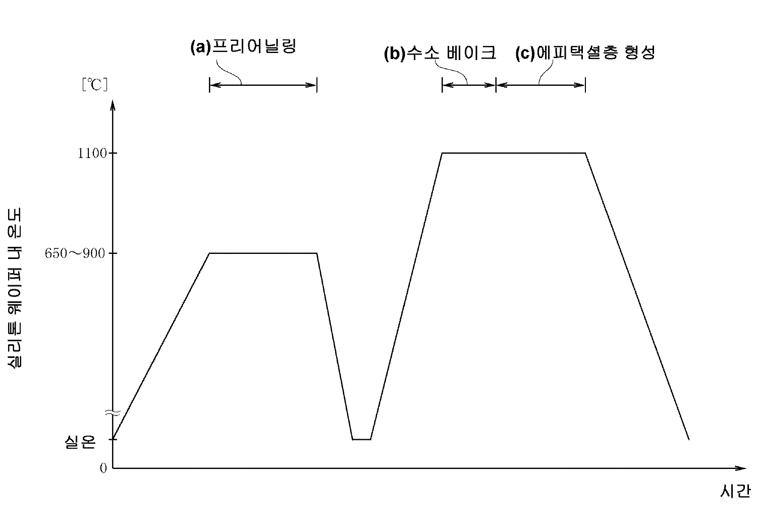
- 보론이 첨가된 실리콘 융액으로부터 실리콘 단결정을 챔버 내에서 초크랄스키법에 의해 인상시키는 공정과, 상기 단결정을 슬라이스하여 얻어진 실리콘 웨이퍼의 표면에 에피택셜층을 형성하는 공정을 포함하는 에피택셜 웨이퍼의 제조 방법에 있어서,상기 단결정은 상기 챔버 내의 인상 도중의 800 내지 600℃의 온도 영역을 250분 이하 180분 이상(강온 속도: 200/180[℃/min] 이하 200/250[℃/min] 이상)에 걸쳐 통과시켜 육성되고,상기 육성된 단결정은 10×1017 내지 12×1017atoms/cm3(ASTM F121-1979) 미만의 산소 농도 및 0.03 내지 0.01Ωcm의 저항률을 가지며,상기 실리콘 웨이퍼의 표면에 에피택셜층을 형성하기 전에 상기 웨이퍼를 불활성 가스 분위기 하 650 내지 900℃의 온도 범위 내의 소정의 온도에서 10분 내지 4시간 유지하는 프리 어닐링을 행하는 것을 특징으로 하는 에피택셜 웨이퍼의 제조 방법.
- 청구항 1에 있어서, 실온에서 프리 어닐링의 소정의 온도로 승온하는 승온 속도가 1 내지 8℃/분이고, 상기 소정의 온도에서 실온까지 냉각하는 강온 속도가 5 내지 2℃/분인 에피택셜 웨이퍼의 제조 방법.
- 보론이 첨가된 실리콘 융액으로부터 실리콘 단결정을 챔버 내에서 강제 냉각하여 챔버 내에서 초크랄스키법에 의해 인상시키는 공정과, 상기 단결정을 슬라이스하여 얻어진 실리콘 웨이퍼의 표면에 에피택셜층을 형성하는 공정을 포함하는 에피택셜 웨이퍼의 제조 방법에 있어서,상기 단결정은 상기 챔버 내의 인상 도중의 800 내지 600℃의 온도 영역을 180분 미만 120분 이상(강온 속도: 200/180[℃/min] 초과 200/120[℃/min] 이하)에 걸쳐 통과시켜 육성되고,상기 육성된 단결정은 10×1017 내지 14×1017atoms/cm3(ASTM F121-1979) 이하의 산소 농도 및 0.03 내지 0.01Ωcm의 저항률을 가지며,상기 실리콘 웨이퍼의 표면에 에피택셜층을 형성하기 전에 상기 웨이퍼를 불활성 가스 분위기 하 650 내지 900℃의 온도 범위 내의 소정의 온도에서 10분 내지 4시간 유지하는 프리 어닐링을 행하는 것을 특징으로 하는 에피택셜 웨이퍼의 제조 방법.
- 청구항 3에 있어서, 실온에서 프리 어닐링의 소정의 온도로 승온하는 승온 속도가 1 내지 8℃/분이고, 상기 소정의 온도에서 실온까지 냉각하는 강온 속도가 5 내지 2℃/분인 에피택셜 웨이퍼의 제조 방법.
- 청구항 3 또는 청구항 4에 있어서, 강제 냉각은 챔버 내에 설치된 수냉식 냉각 장치에 의해 행해지는 에피택셜 웨이퍼의 제조 방법.
- 800 내지 600℃의 온도 영역을 250분 이하 180분 이상(강온 속도: 200/180[℃/min] 이하 200/250[℃/min] 이상)에 걸쳐 통과시켜 육성된 단결정을 이용하여 제조되고, 웨이퍼의 에피택셜층 표면에서 0.09μm 이상의 크기의 에피택셜 결함이 3개/장 이하의 밀도를 가지며, 상기 에피택셜층을 제외한 상기 웨이퍼 내부에 형성되는 산소 석출물 밀도가 1×10⁴개/cm2 이상인 것을 특징으로 하는 에피택셜 웨이퍼.
- 800 내지 600℃의 온도 영역을 180분 미만 120분 이상(강온 속도: 200/180[℃/min] 초과 200/120[℃/min] 이하)에 걸쳐 통과시켜 육성된 단결정을 이용하여 제조되고, 웨이퍼의 에피택셜층 표면에서 0.09μm 이상의 크기의 에피택셜 결함이 3개/장 이하의 밀도를 가지며, 상기 에피택셜층을 제외한 상기 웨이퍼 내부에 형성되는 산소 석출물 밀도가 1×10⁴개/cm2 이상인 것을 특징으로 하는 에피택셜 웨이퍼.
Applications Claiming Priority (2)
| Application Number | Priority Date | Filing Date | Title |
|---|---|---|---|
| JPJP-P-2006-00300644 | 2006-11-06 | ||
| JP2006300644A JP4853237B2 (ja) | 2006-11-06 | 2006-11-06 | エピタキシャルウェーハの製造方法 |
Publications (2)
| Publication Number | Publication Date |
|---|---|
| KR20080041128A KR20080041128A (ko) | 2008-05-09 |
| KR100933552B1 true KR100933552B1 (ko) | 2009-12-23 |
Family
ID=38969955
Family Applications (1)
| Application Number | Title | Priority Date | Filing Date |
|---|---|---|---|
| KR1020070112483A Active KR100933552B1 (ko) | 2006-11-06 | 2007-11-06 | 에피택셜 웨이퍼의 제조 방법 |
Country Status (5)
| Country | Link |
|---|---|
| US (1) | US8920560B2 (ko) |
| EP (1) | EP1926134B1 (ko) |
| JP (1) | JP4853237B2 (ko) |
| KR (1) | KR100933552B1 (ko) |
| TW (1) | TWI365235B (ko) |
Families Citing this family (15)
| Publication number | Priority date | Publication date | Assignee | Title |
|---|---|---|---|---|
| JP4805681B2 (ja) * | 2006-01-12 | 2011-11-02 | ジルトロニック アクチエンゲゼルシャフト | エピタキシャルウェーハおよびエピタキシャルウェーハの製造方法 |
| JP5136518B2 (ja) * | 2008-06-16 | 2013-02-06 | 株式会社Sumco | シリコン単結晶の育成方法 |
| JP5555995B2 (ja) * | 2008-09-12 | 2014-07-23 | 株式会社Sumco | 貼り合わせシリコンウェーハの製造方法 |
| JP2011054821A (ja) * | 2009-09-03 | 2011-03-17 | Sumco Corp | エピタキシャルウェーハの製造方法及びエピタキシャルウェーハ |
| JP2011082443A (ja) * | 2009-10-09 | 2011-04-21 | Sumco Corp | エピタキシャルウェーハおよびその製造方法 |
| JP5194146B2 (ja) * | 2010-12-28 | 2013-05-08 | ジルトロニック アクチエンゲゼルシャフト | シリコン単結晶の製造方法、シリコン単結晶、およびウエハ |
| US11180866B2 (en) * | 2013-04-10 | 2021-11-23 | Kla Corporation | Passivation of nonlinear optical crystals |
| KR101729515B1 (ko) * | 2015-04-14 | 2017-04-24 | 주식회사 엘지실트론 | 실리콘 단결정 잉곳의 성장 방법 |
| JP6447351B2 (ja) | 2015-05-08 | 2019-01-09 | 株式会社Sumco | シリコンエピタキシャルウェーハの製造方法およびシリコンエピタキシャルウェーハ |
| JP6610056B2 (ja) | 2015-07-28 | 2019-11-27 | 株式会社Sumco | エピタキシャルシリコンウェーハの製造方法 |
| JP6631460B2 (ja) * | 2016-10-03 | 2020-01-15 | 株式会社Sumco | シリコン単結晶の製造方法およびシリコン単結晶 |
| DE102017213587A1 (de) * | 2017-08-04 | 2019-02-07 | Siltronic Ag | Halbleiterscheibe aus einkristallinem Silizium und Verfahren zur Herstellung der Halbleiterscheibe |
| CN113862791A (zh) * | 2021-09-28 | 2021-12-31 | 西安奕斯伟材料科技有限公司 | 一种用于拉制单晶硅棒的拉晶炉 |
| CN113862777B (zh) * | 2021-09-30 | 2023-05-16 | 西安奕斯伟材料科技股份有限公司 | 一种用于制造单晶硅棒的拉晶炉、方法及单晶硅棒 |
| JP7770907B2 (ja) * | 2021-12-22 | 2025-11-17 | グローバルウェーハズ・ジャパン株式会社 | シリコンエピタキシャル基板の製造方法およびシリコンエピタキシャル基板 |
Citations (2)
| Publication number | Priority date | Publication date | Assignee | Title |
|---|---|---|---|---|
| KR20000057350A (ko) * | 1996-12-03 | 2000-09-15 | 고지마 마타오 | 반도체 실리콘 에피택셜 웨이퍼 및 반도체 디바이스의 제조 방법 |
| JP2004091221A (ja) * | 2002-08-29 | 2004-03-25 | Sumitomo Mitsubishi Silicon Corp | シリコン単結晶とエピタキシャルウェーハ並びにそれらの製造方法 |
Family Cites Families (20)
| Publication number | Priority date | Publication date | Assignee | Title |
|---|---|---|---|---|
| JP3006669B2 (ja) * | 1995-06-20 | 2000-02-07 | 信越半導体株式会社 | 結晶欠陥の均一なシリコン単結晶の製造方法およびその製造装置 |
| JPH10223641A (ja) * | 1996-12-03 | 1998-08-21 | Sumitomo Sitix Corp | 半導体シリコンエピタキシャルウェーハ及び半導体デバイスの製造方法 |
| JP2000016897A (ja) * | 1998-07-03 | 2000-01-18 | Sumitomo Metal Ind Ltd | 高品質シリコン単結晶の製造方法 |
| JP4233651B2 (ja) * | 1998-10-29 | 2009-03-04 | 信越半導体株式会社 | シリコン単結晶ウエーハ |
| JP3601324B2 (ja) * | 1998-11-19 | 2004-12-15 | 信越半導体株式会社 | 結晶欠陥の少ないシリコン単結晶ウエーハ及びその製造方法 |
| JP3855531B2 (ja) | 1999-04-23 | 2006-12-13 | 株式会社Sumco | ポリシリコン層付きシリコンウェーハ及びその製造方法 |
| JP4107628B2 (ja) | 1999-11-26 | 2008-06-25 | 株式会社Sumco | シリコンウェーハにig効果を付与するための前熱処理方法 |
| JP4003351B2 (ja) | 1999-07-28 | 2007-11-07 | 株式会社Sumco | Ig処理法 |
| TW528816B (en) | 1999-04-23 | 2003-04-21 | Mitsubishi Material Silicon | Method for heat treating silicon wafer |
| US20020142170A1 (en) * | 1999-07-28 | 2002-10-03 | Sumitomo Metal Industries, Ltd. | Silicon single crystal, silicon wafer, and epitaxial wafer |
| JP2001217251A (ja) | 1999-11-26 | 2001-08-10 | Mitsubishi Materials Silicon Corp | シリコンウェーハの熱処理方法 |
| JP2001253795A (ja) * | 2000-03-09 | 2001-09-18 | Sumitomo Metal Ind Ltd | シリコンエピタキシャルウェーハとその製造方法 |
| KR100368331B1 (ko) * | 2000-10-04 | 2003-01-24 | 주식회사 실트론 | 반도체 웨이퍼의 열처리 방법 및 이를 통해 제조된 반도체 웨이퍼 |
| US6835245B2 (en) * | 2000-06-22 | 2004-12-28 | Sumitomo Mitsubishi Silicon Corporation | Method of manufacturing epitaxial wafer and method of producing single crystal as material therefor |
| US6547875B1 (en) * | 2000-09-25 | 2003-04-15 | Mitsubishi Materials Silicon Corporation | Epitaxial wafer and a method for manufacturing the same |
| JP3624827B2 (ja) * | 2000-12-20 | 2005-03-02 | 三菱住友シリコン株式会社 | シリコン単結晶の製造方法 |
| US6846539B2 (en) * | 2001-01-26 | 2005-01-25 | Memc Electronic Materials, Inc. | Low defect density silicon having a vacancy-dominated core substantially free of oxidation induced stacking faults |
| US6709957B2 (en) * | 2001-06-19 | 2004-03-23 | Sumitomo Mitsubishi Silicon Corporation | Method of producing epitaxial wafers |
| JP2004091211A (ja) * | 2002-07-12 | 2004-03-25 | Oki Data Corp | 媒体トレイ及びこれを用いた画像記録装置 |
| WO2005014898A1 (ja) * | 2003-08-12 | 2005-02-17 | Shin-Etsu Handotai Co.,Ltd. | ウエーハの製造方法 |
-
2006
- 2006-11-06 JP JP2006300644A patent/JP4853237B2/ja active Active
-
2007
- 2007-10-26 EP EP07021018.2A patent/EP1926134B1/en active Active
- 2007-10-29 TW TW096140611A patent/TWI365235B/zh active
- 2007-11-02 US US11/934,461 patent/US8920560B2/en active Active
- 2007-11-06 KR KR1020070112483A patent/KR100933552B1/ko active Active
Patent Citations (2)
| Publication number | Priority date | Publication date | Assignee | Title |
|---|---|---|---|---|
| KR20000057350A (ko) * | 1996-12-03 | 2000-09-15 | 고지마 마타오 | 반도체 실리콘 에피택셜 웨이퍼 및 반도체 디바이스의 제조 방법 |
| JP2004091221A (ja) * | 2002-08-29 | 2004-03-25 | Sumitomo Mitsubishi Silicon Corp | シリコン単結晶とエピタキシャルウェーハ並びにそれらの製造方法 |
Also Published As
| Publication number | Publication date |
|---|---|
| TW200829732A (en) | 2008-07-16 |
| US20080286565A1 (en) | 2008-11-20 |
| KR20080041128A (ko) | 2008-05-09 |
| EP1926134A1 (en) | 2008-05-28 |
| JP4853237B2 (ja) | 2012-01-11 |
| TWI365235B (en) | 2012-06-01 |
| US8920560B2 (en) | 2014-12-30 |
| JP2008115050A (ja) | 2008-05-22 |
| EP1926134B1 (en) | 2016-03-30 |
Similar Documents
| Publication | Publication Date | Title |
|---|---|---|
| KR100933552B1 (ko) | 에피택셜 웨이퍼의 제조 방법 | |
| JP5072460B2 (ja) | 半導体用シリコンウエハ、およびその製造方法 | |
| KR100461893B1 (ko) | 실리콘 웨이퍼 및 이것에 사용되는 실리콘 단결정의제조방법 | |
| JP5537802B2 (ja) | シリコンウエハの製造方法 | |
| JP5515406B2 (ja) | シリコンウェーハおよびその製造方法 | |
| KR100710702B1 (ko) | 실리콘 단결정의 제조 방법, 단결정 잉곳 제조 장치 및실리콘 단결정 웨이퍼의 열처리 방법 | |
| KR20100014191A (ko) | 실리콘 웨이퍼, 실리콘 웨이퍼의 제조방법, 및 실리콘 웨이퍼의 열처리 방법 | |
| KR101684873B1 (ko) | 실리콘 기판의 제조 방법 및 실리콘 기판 | |
| EP0942077B1 (en) | A method for producing a silicon single crystal wafer and a silicon single crystal wafer | |
| JP2004304095A (ja) | シリコンウェーハおよびその製造方法 | |
| KR100582241B1 (ko) | 질소 도프된 저결함 실리콘 단결정의 제조방법 | |
| KR20010101189A (ko) | 에피텍셜 웨이퍼용 실리콘 단결정 웨이퍼, 에피텍셜웨이퍼 및 이들의 제조방법 그리고 평가방법 | |
| KR20060040733A (ko) | 웨이퍼의 제조방법 | |
| JP3614019B2 (ja) | シリコン単結晶ウエーハの製造方法およびシリコン単結晶ウエーハ | |
| KR20140021543A (ko) | 실리콘 기판의 제조방법 및 실리콘 기판 | |
| KR100526427B1 (ko) | 실리콘 반도체기판 및 그 제조방법 | |
| US6709957B2 (en) | Method of producing epitaxial wafers | |
| JP2001199794A (ja) | シリコン単結晶インゴット、その製造方法およびシリコンウェーハの製造方法 | |
| JP4089137B2 (ja) | シリコン単結晶の製造方法およびエピタキシャルウェーハの製造方法 | |
| JP2004091221A (ja) | シリコン単結晶とエピタキシャルウェーハ並びにそれらの製造方法 | |
| TWI828442B (zh) | 磊晶晶圓 | |
| JP2004172391A (ja) | シリコンウェーハおよびその製造方法 |
Legal Events
| Date | Code | Title | Description |
|---|---|---|---|
| A201 | Request for examination | ||
| PA0109 | Patent application |
St.27 status event code: A-0-1-A10-A12-nap-PA0109 |
|
| PA0201 | Request for examination |
St.27 status event code: A-1-2-D10-D11-exm-PA0201 |
|
| PG1501 | Laying open of application |
St.27 status event code: A-1-1-Q10-Q12-nap-PG1501 |
|
| D13-X000 | Search requested |
St.27 status event code: A-1-2-D10-D13-srh-X000 |
|
| D14-X000 | Search report completed |
St.27 status event code: A-1-2-D10-D14-srh-X000 |
|
| E902 | Notification of reason for refusal | ||
| PE0902 | Notice of grounds for rejection |
St.27 status event code: A-1-2-D10-D21-exm-PE0902 |
|
| P11-X000 | Amendment of application requested |
St.27 status event code: A-2-2-P10-P11-nap-X000 |
|
| P13-X000 | Application amended |
St.27 status event code: A-2-2-P10-P13-nap-X000 |
|
| E701 | Decision to grant or registration of patent right | ||
| PE0701 | Decision of registration |
St.27 status event code: A-1-2-D10-D22-exm-PE0701 |
|
| GRNT | Written decision to grant | ||
| PR0701 | Registration of establishment |
St.27 status event code: A-2-4-F10-F11-exm-PR0701 |
|
| PR1002 | Payment of registration fee |
St.27 status event code: A-2-2-U10-U11-oth-PR1002 Fee payment year number: 1 |
|
| PG1601 | Publication of registration |
St.27 status event code: A-4-4-Q10-Q13-nap-PG1601 |
|
| FPAY | Annual fee payment |
Payment date: 20121207 Year of fee payment: 4 |
|
| PR1001 | Payment of annual fee |
St.27 status event code: A-4-4-U10-U11-oth-PR1001 Fee payment year number: 4 |
|
| FPAY | Annual fee payment |
Payment date: 20131206 Year of fee payment: 5 |
|
| PR1001 | Payment of annual fee |
St.27 status event code: A-4-4-U10-U11-oth-PR1001 Fee payment year number: 5 |
|
| FPAY | Annual fee payment |
Payment date: 20141205 Year of fee payment: 6 |
|
| PR1001 | Payment of annual fee |
St.27 status event code: A-4-4-U10-U11-oth-PR1001 Fee payment year number: 6 |
|
| FPAY | Annual fee payment |
Payment date: 20151204 Year of fee payment: 7 |
|
| PR1001 | Payment of annual fee |
St.27 status event code: A-4-4-U10-U11-oth-PR1001 Fee payment year number: 7 |
|
| FPAY | Annual fee payment |
Payment date: 20161205 Year of fee payment: 8 |
|
| PR1001 | Payment of annual fee |
St.27 status event code: A-4-4-U10-U11-oth-PR1001 Fee payment year number: 8 |
|
| FPAY | Annual fee payment |
Payment date: 20171208 Year of fee payment: 9 |
|
| PR1001 | Payment of annual fee |
St.27 status event code: A-4-4-U10-U11-oth-PR1001 Fee payment year number: 9 |
|
| PR1001 | Payment of annual fee |
St.27 status event code: A-4-4-U10-U11-oth-PR1001 Fee payment year number: 10 |
|
| PR1001 | Payment of annual fee |
St.27 status event code: A-4-4-U10-U11-oth-PR1001 Fee payment year number: 11 |
|
| PR1001 | Payment of annual fee |
St.27 status event code: A-4-4-U10-U11-oth-PR1001 Fee payment year number: 12 |
|
| PR1001 | Payment of annual fee |
St.27 status event code: A-4-4-U10-U11-oth-PR1001 Fee payment year number: 13 |
|
| PR1001 | Payment of annual fee |
St.27 status event code: A-4-4-U10-U11-oth-PR1001 Fee payment year number: 14 |
|
| PR1001 | Payment of annual fee |
St.27 status event code: A-4-4-U10-U11-oth-PR1001 Fee payment year number: 15 |
|
| PR1001 | Payment of annual fee |
St.27 status event code: A-4-4-U10-U11-oth-PR1001 Fee payment year number: 16 |
|
| P22-X000 | Classification modified |
St.27 status event code: A-4-4-P10-P22-nap-X000 |