KR100933552B1 - Method of manufacturing epitaxial wafer - Google Patents
Method of manufacturing epitaxial wafer Download PDFInfo
- Publication number
- KR100933552B1 KR100933552B1 KR1020070112483A KR20070112483A KR100933552B1 KR 100933552 B1 KR100933552 B1 KR 100933552B1 KR 1020070112483 A KR1020070112483 A KR 1020070112483A KR 20070112483 A KR20070112483 A KR 20070112483A KR 100933552 B1 KR100933552 B1 KR 100933552B1
- Authority
- KR
- South Korea
- Prior art keywords
- single crystal
- epitaxial
- wafer
- temperature
- minutes
- Prior art date
- Legal status (The legal status is an assumption and is not a legal conclusion. Google has not performed a legal analysis and makes no representation as to the accuracy of the status listed.)
- Active
Links
Images


Classifications
-
- C—CHEMISTRY; METALLURGY
- C30—CRYSTAL GROWTH
- C30B—SINGLE-CRYSTAL GROWTH; UNIDIRECTIONAL SOLIDIFICATION OF EUTECTIC MATERIAL OR UNIDIRECTIONAL DEMIXING OF EUTECTOID MATERIAL; REFINING BY ZONE-MELTING OF MATERIAL; PRODUCTION OF A HOMOGENEOUS POLYCRYSTALLINE MATERIAL WITH DEFINED STRUCTURE; SINGLE CRYSTALS OR HOMOGENEOUS POLYCRYSTALLINE MATERIAL WITH DEFINED STRUCTURE; AFTER-TREATMENT OF SINGLE CRYSTALS OR A HOMOGENEOUS POLYCRYSTALLINE MATERIAL WITH DEFINED STRUCTURE; APPARATUS THEREFOR
- C30B15/00—Single-crystal growth by pulling from a melt, e.g. Czochralski method
- C30B15/20—Controlling or regulating
- C30B15/206—Controlling or regulating the thermal history of growing the ingot
-
- H—ELECTRICITY
- H10—SEMICONDUCTOR DEVICES; ELECTRIC SOLID-STATE DEVICES NOT OTHERWISE PROVIDED FOR
- H10P—GENERIC PROCESSES OR APPARATUS FOR THE MANUFACTURE OR TREATMENT OF DEVICES COVERED BY CLASS H10
- H10P14/00—Formation of materials, e.g. in the shape of layers or pillars
- H10P14/20—Formation of materials, e.g. in the shape of layers or pillars of semiconductor materials
-
- C—CHEMISTRY; METALLURGY
- C30—CRYSTAL GROWTH
- C30B—SINGLE-CRYSTAL GROWTH; UNIDIRECTIONAL SOLIDIFICATION OF EUTECTIC MATERIAL OR UNIDIRECTIONAL DEMIXING OF EUTECTOID MATERIAL; REFINING BY ZONE-MELTING OF MATERIAL; PRODUCTION OF A HOMOGENEOUS POLYCRYSTALLINE MATERIAL WITH DEFINED STRUCTURE; SINGLE CRYSTALS OR HOMOGENEOUS POLYCRYSTALLINE MATERIAL WITH DEFINED STRUCTURE; AFTER-TREATMENT OF SINGLE CRYSTALS OR A HOMOGENEOUS POLYCRYSTALLINE MATERIAL WITH DEFINED STRUCTURE; APPARATUS THEREFOR
- C30B25/00—Single-crystal growth by chemical reaction of reactive gases, e.g. chemical vapour-deposition growth
- C30B25/02—Epitaxial-layer growth
- C30B25/18—Epitaxial-layer growth characterised by the substrate
- C30B25/20—Epitaxial-layer growth characterised by the substrate the substrate being of the same materials as the epitaxial layer
-
- C—CHEMISTRY; METALLURGY
- C30—CRYSTAL GROWTH
- C30B—SINGLE-CRYSTAL GROWTH; UNIDIRECTIONAL SOLIDIFICATION OF EUTECTIC MATERIAL OR UNIDIRECTIONAL DEMIXING OF EUTECTOID MATERIAL; REFINING BY ZONE-MELTING OF MATERIAL; PRODUCTION OF A HOMOGENEOUS POLYCRYSTALLINE MATERIAL WITH DEFINED STRUCTURE; SINGLE CRYSTALS OR HOMOGENEOUS POLYCRYSTALLINE MATERIAL WITH DEFINED STRUCTURE; AFTER-TREATMENT OF SINGLE CRYSTALS OR A HOMOGENEOUS POLYCRYSTALLINE MATERIAL WITH DEFINED STRUCTURE; APPARATUS THEREFOR
- C30B29/00—Single crystals or homogeneous polycrystalline material with defined structure characterised by the material or by their shape
- C30B29/02—Elements
- C30B29/06—Silicon
-
- C—CHEMISTRY; METALLURGY
- C30—CRYSTAL GROWTH
- C30B—SINGLE-CRYSTAL GROWTH; UNIDIRECTIONAL SOLIDIFICATION OF EUTECTIC MATERIAL OR UNIDIRECTIONAL DEMIXING OF EUTECTOID MATERIAL; REFINING BY ZONE-MELTING OF MATERIAL; PRODUCTION OF A HOMOGENEOUS POLYCRYSTALLINE MATERIAL WITH DEFINED STRUCTURE; SINGLE CRYSTALS OR HOMOGENEOUS POLYCRYSTALLINE MATERIAL WITH DEFINED STRUCTURE; AFTER-TREATMENT OF SINGLE CRYSTALS OR A HOMOGENEOUS POLYCRYSTALLINE MATERIAL WITH DEFINED STRUCTURE; APPARATUS THEREFOR
- C30B33/00—After-treatment of single crystals or homogeneous polycrystalline material with defined structure
- C30B33/02—Heat treatment
-
- H—ELECTRICITY
- H10—SEMICONDUCTOR DEVICES; ELECTRIC SOLID-STATE DEVICES NOT OTHERWISE PROVIDED FOR
- H10P—GENERIC PROCESSES OR APPARATUS FOR THE MANUFACTURE OR TREATMENT OF DEVICES COVERED BY CLASS H10
- H10P36/00—Gettering within semiconductor bodies
- H10P36/20—Intrinsic gettering, i.e. thermally inducing defects by using oxygen present in the silicon body
-
- Y—GENERAL TAGGING OF NEW TECHNOLOGICAL DEVELOPMENTS; GENERAL TAGGING OF CROSS-SECTIONAL TECHNOLOGIES SPANNING OVER SEVERAL SECTIONS OF THE IPC; TECHNICAL SUBJECTS COVERED BY FORMER USPC CROSS-REFERENCE ART COLLECTIONS [XRACs] AND DIGESTS
- Y10—TECHNICAL SUBJECTS COVERED BY FORMER USPC
- Y10T—TECHNICAL SUBJECTS COVERED BY FORMER US CLASSIFICATION
- Y10T428/00—Stock material or miscellaneous articles
- Y10T428/26—Web or sheet containing structurally defined element or component, the element or component having a specified physical dimension
Landscapes
- Chemical & Material Sciences (AREA)
- Engineering & Computer Science (AREA)
- Crystallography & Structural Chemistry (AREA)
- Materials Engineering (AREA)
- Metallurgy (AREA)
- Organic Chemistry (AREA)
- Physics & Mathematics (AREA)
- Thermal Sciences (AREA)
- Chemical Kinetics & Catalysis (AREA)
- General Chemical & Material Sciences (AREA)
- Crystals, And After-Treatments Of Crystals (AREA)
- Chemical Vapour Deposition (AREA)
Abstract
에피택셜 결함의 발생을 저감할 수 있고 IG 효과가 뛰어난 직경 300mm 이상의 에피택셜 웨이퍼를 얻는다.
보론이 첨가된 실리콘 융액(11)으로부터 단결정(12)을 챔버(21) 내에서 초크랄스키법에 의해 인상시키는 공정과, 단결정을 슬라이스하여 얻어진 실리콘 웨이퍼의 표면에 에피택셜층을 형성하는 공정을 포함하는 에피택셜 웨이퍼의 제조 방법이다. 단결정은 챔버 내의 인상 도중의 800 내지 600℃의 온도 영역을 250 내지 180분에 걸쳐 통과시켜 육성된다. 단결정은 산소 농도 10×1017 내지 12×1017atoms/cm3 및 저항률 0.03 내지 0.01Ωcm를 갖는다. 웨이퍼의 표면에 에피택셜층을 형성하기 전에 웨이퍼를 불활성 가스 분위기 하 650 내지 900℃의 온도 범위 내의 소정의 온도에서 10분 내지 4시간 유지하는 프리 어닐링을 행한다.
에피택셜, 단결정, 실리콘, 결함, 산소, 보론, 초크랄스키법, 웨이퍼, 인상
The epitaxial wafer of 300 mm or more in diameter which can reduce the occurrence of epitaxial defects and is excellent in IG effect is obtained.
The step of pulling up the single crystal 12 from the boron-doped silicon melt 11 by the Czochralski method in the chamber 21 and the step of forming an epitaxial layer on the surface of the silicon wafer obtained by slicing the single crystal It is a manufacturing method of an epitaxial wafer containing. The single crystal is grown by passing a temperature range of 800 to 600 ° C. during the pulling in the chamber over 250 to 180 minutes. The single crystal has an oxygen concentration of 10 × 10 17 to 12 × 10 17 atoms / cm 3 and a resistivity of 0.03 to 0.01 Ωcm. Prior to forming the epitaxial layer on the surface of the wafer, pre-annealing is performed for 10 minutes to 4 hours at a predetermined temperature within a temperature range of 650 to 900 ° C. under an inert gas atmosphere.
Epitaxial, single crystal, silicon, defect, oxygen, boron, Czochralski, wafer, impression
Description
본 발명은 반도체용 고집적도 디바이스에 사용되는 에피택셜 웨이퍼의 제조 방법의 개량에 관한 것이다. 더욱 상세하게는, 초크랄스키법(이하, CZ법이라고 함.)에 의해 육성된 실리콘 단결정을 슬라이스하여 얻어진 실리콘 웨이퍼 상에 에피택셜층을 형성하는 에피택셜 웨이퍼의 제조 방법에 관한 것이다. TECHNICAL FIELD This invention relates to the improvement of the manufacturing method of an epitaxial wafer used for the high density device for semiconductors. More specifically, the present invention relates to a method for producing an epitaxial wafer in which an epitaxial layer is formed on a silicon wafer obtained by slicing silicon single crystals grown by the Czochralski method (hereinafter referred to as CZ method).
종래 고집적도 디바이스의 기판으로 사용되는 에피택셜 웨이퍼(epitaxial wafer)는 초크랄스키법(이하, CZ법이라고 함.)에 의해 육성된 실리콘 단결정을 슬라이스하여 얻어진 실리콘 웨이퍼 상에 에피택셜층을 형성함으로써 제조된다. An epitaxial wafer used as a substrate of a conventional high-density device is formed by slicing a silicon single crystal grown by the Czochralski method (hereinafter referred to as CZ method) by forming an epitaxial layer on a silicon wafer. Are manufactured.
CZ법은 도가니의 내부에 충전한 실리콘 다결정을 히터로 가열 용융한 후, 이 융액의 표면에 시드 결정(종자 결정)을 담그고, 이것을 회전시키면서 성장시키고 상방으로 인상으로써 단결정을 육성시키는 방법이다. 이 CZ법으로 육성한 단결정으로부터 얻어진 실리콘 웨이퍼(이하, 에피 서브 웨이퍼라고 함.)의 표면에 전위나 산화 유기 적층 결함(oxygen-induced stacking faults, 이하, OSF라고 함.) 등의 결정 결함이 존재하면 에피 서브 웨이퍼 표면에 형성된 에피택셜층에는 이들 결함에 기인한 에피택셜 결함이 존재한다. The CZ method is a method of growing a single crystal by heating and melting a silicon polycrystal filled in a crucible with a heater, immersing seed crystals (seed crystals) on the surface of the melt, growing them while rotating them, and pulling them upwards. Crystal defects such as dislocations and oxygen-induced stacking faults (hereinafter referred to as OSFs) exist on the surface of a silicon wafer (hereinafter referred to as an epi sub wafer) obtained from a single crystal grown by the CZ method. Epitaxial defects due to these defects exist in the epitaxial layer formed on the lower surface of the epi sub wafer.
이 에피택셜 결함은 디바이스의 고집적화가 진행되어 미세화된 회로 패턴을 형성하는 웨이퍼 상의 디바이스 활성 영역에서 누설 전류의 증가나 라이프 타임의 저하 원인이 되기 때문에, 그의 저감, 제거가 요구되고 있다. This epitaxial defect is required to reduce and remove the device because of high integration of the device, which leads to an increase in leakage current and a decrease in life time in the device active region on the wafer forming a miniaturized circuit pattern.
그러나, 에피택셜 결함이 적고 결정의 완전성이 높은 에피택셜 웨이퍼를 사용하여도 그 후의 디바이스 공정에서 금속 불순물로 인해 에피택셜층이 오염됨으로써 디바이스 특성이 악화되는 문제가 있다. However, even if an epitaxial wafer having fewer epitaxial defects and high crystal integrity is used, there is a problem in that device characteristics are deteriorated due to contamination of the epitaxial layer due to metal impurities in subsequent device processes.
이러한 금속계 원소의 불순물으로 인한 에피택셜층의 오염은 디바이스의 집적이 고밀도화될수록 프로세스도 복잡해져 그 기회가 증가하여 영향도 커지게 된다. 금속 오염의 배제는 기본적으로는 프로세스 환경 및 사용 재료의 클린화에 있는데, 디바이스 프로세스에서 금속 오염을 완전히 없애기는 어려우며, 그 대처 수단으로서 에피 서브 웨이퍼에서의 게터링 기술의 개발이 중요해진다. 이 게터링 기술은 오염에 의해 에피택셜층으로 침입해 온 불순물 원소를 디바이스 활성 영역 이외의 장소(싱크)에 포획하고 디바이스 활성 영역에서 무해화하는 수단이다. The contamination of the epitaxial layer due to the impurities of the metal-based element becomes more complicated as the integration of the device becomes dense, and the chance increases, and the influence also increases. The exclusion of metal contamination is basically the cleanliness of the process environment and the materials used, and it is difficult to completely eliminate metal contamination in the device process, and as a countermeasure, development of gettering technology in epi sub wafers becomes important. This gettering technique is a means for trapping impurity elements that have penetrated into the epitaxial layer due to contamination in a place (sink) other than the device active region and making it harmless in the device active region.
게터링 기술로는 디바이스 프로세스의 열처리 중에 유기되는 산소에 기인한 미소한 산소 석출물(Bulk Micro Defect, 이하, BMD라고 함.)을 이용하여 불순물 원소를 포획하는 인트린식 게터링(intrinsic gettering, 이하, IG라고 함.)이라 불리는 것이 있다. 그러나, 에피택셜층 형성 공정의 1050 내지 1200℃의 고온 열처리가 실리콘 웨이퍼에 실시됨으로써 실리콘 단결정을 슬라이스하여 얻어진 웨이퍼에 내재하는 미소한 산소 석출 핵이 축소, 소멸되고, 그 후의 디바이스 프로세스에서 웨이퍼 내에 게터링원인 BMD를 충분히 유기하기가 어려워진다. 따라서, 이 게터링 기술을 적용하여도 프로세스 전체에 걸쳐 금속 불순물에 대하여 충분한 IG 효과를 바랄 수 없다는 문제가 생긴다. The gettering technique includes intrinsic gettering, which captures impurity elements using minute oxygen precipitates (Bulk Micro Defect, hereinafter referred to as BMD) due to the oxygen induced during the heat treatment of the device process. IG). However, the high temperature heat treatment at 1050 to 1200 ° C. of the epitaxial layer forming step is performed on the silicon wafer, whereby the minute oxygen precipitation nuclei inherent in the wafer obtained by slicing the silicon single crystal are reduced and extinguished. It is difficult to sufficiently abandon the turbid source BMD. Therefore, even if this gettering technique is applied, there arises a problem that a sufficient IG effect cannot be desired for metal impurities throughout the process.
따라서, 에피택셜 결함의 발생을 저감하고 IG 효과가 뛰어난 에피택셜 웨이퍼를 얻기 위한 제조 방법이 제안된 바 있다(예컨대, 특허 문헌 1 참조.). 이 방법은 단결정 인상 중의 1100 내지 900℃의 온도 영역을 3.0℃/분 이상의 냉각 속도로 급속 냉각(이하, 급냉이라고 함.)하고, 산소 석출 핵의 크기를 미소화시킴으로써 에피택셜 결함의 발생을 현저하게 억제하는 것이다. Therefore, a manufacturing method for reducing the occurrence of epitaxial defects and obtaining an epitaxial wafer having an excellent IG effect has been proposed (see Patent Document 1, for example). This method rapidly cools the temperature range of 1100 to 900 ° C. during the single crystal pulling at a cooling rate of 3.0 ° C./min or more (hereinafter, referred to as quenching), and reduces the occurrence of epitaxial defects by minimizing the size of the oxygen precipitation nuclei. It is to suppress.
구체적으로는, 이 방법은 보론이 첨가된 실리콘 융액이 들어간 도가니로부터 직경 200mm의 실리콘 단결정을 챔버 내에서 CZ법에 의해 육성할 때 단결정을 인상 속도 1.1mm/분으로 500mm의 길이까지 인상시켜 직동부를 형성하고, 그 후 인상 속도를 1.8mm/분으로 상승시켜 550mm의 길이까지 인상시킨다. 계속하여 다시 인상 속도를 1.1mm/분으로 되돌리고, 그대로 단결정을 1000mm의 길이까지 인상시킨다. 이와 같이 인상 속도를 변화시킴으로써 인상 중의 1100 내지 900℃의 온도 영역을 3℃/분 이상의 냉각 속도로 단결정을 급냉시킬 수 있다. 이 단결정을 슬라이스하여 얻어진 실리콘 웨이퍼를 산소와 불활성(비활성) 가스의 혼합 분위기 중에서 850℃에서 2시간 열처리를 행한다. 이 열처리에 의해 실리콘 웨이퍼의 결정 중의 산소 석출 핵의 열적 안정성이 증가하기 때문에 에피택셜층 형성 공정의 고온 열처리에 의해서도 BMD가 축소 또는 소멸되지 않는다. 그리고, 이 열처리 후의 실리콘 웨이퍼에 경면 연마를 실시한 후, 에피택셜 장치에 실리콘 웨이퍼를 수용하고, 1150℃ 1분간의 수소 베이크 처리에 이어 장치 내 온도를 1075℃로 하여 소정 시간 유지하면서 원료 가스를 공급함으로써 웨이퍼 표면에 5μm의 두께의 에피택셜층을 형성하여 에피택셜 웨이퍼를 얻을 수 있다. Specifically, in this method, when a silicon single crystal having a diameter of 200 mm is grown in a chamber by a CZ method from a crucible containing a silicon melt containing boron, the single crystal is pulled up to a length of 500 mm at a pulling speed of 1.1 mm / min. And then the pulling speed is raised to 1.8 mm / min to a length of 550 mm. Subsequently, the pulling speed is returned to 1.1 mm / min, and the single crystal is pulled up to a length of 1000 mm as it is. By changing the pulling speed in this manner, the single crystal can be quenched at a cooling rate of 3 ° C / min or more in the temperature range of 1100 to 900 ° C in the pulling. The silicon wafer obtained by slicing this single crystal is heat-treated at 850 ° C. for 2 hours in a mixed atmosphere of oxygen and an inert (inactive) gas. Since the thermal stability of the oxygen precipitate nuclei in the crystal of the silicon wafer is increased by this heat treatment, the BMD is not reduced or extinct even by the high temperature heat treatment in the epitaxial layer forming step. After performing the mirror polishing on the silicon wafer after the heat treatment, the silicon wafer is accommodated in the epitaxial device, and the raw material gas is supplied while maintaining the internal temperature at 1075 ° C. for a predetermined time after hydrogen baking for 1 minute at 1150 ° C. for 1 minute. As a result, an epitaxial layer having a thickness of 5 m can be formed on the wafer surface to obtain an epitaxial wafer.
[특허 문헌 1] 일본 특허 공개 2004-91221호 공보(청구항 5, 청구항 7, 명세서 [0013] 내지 [0017], [0023], [0024], [0026], [0027], 도 1)[Patent Document 1] Japanese Patent Application Laid-Open No. 2004-91221 (claim 5, claim 7, specifications [0013] to [0023], [0024], [0026], [0027], and FIG. 1)
그러나, 실리콘 단결정 인상 공정에서 그 중심부는 잘 냉각되지 않고 외주부는 냉각되기 쉽다는 구조상의 이유로 인해, 단결정의 냉각 속도는 중심부와 외주부에서 서로 다른 경향이 있다. 이 경향은 직경 300mm 이상의 단결정에서 보다 현저해지며, 단결정 중심부에서 냉각 속도 3℃/분 이상의 급냉 조건을 달성하기는 어려워진다. 만일 냉각체 설치에 의해 냉각 속도 3℃/분 이상의 급냉 조건을 달성할 수 있었다고 해도, 단결정에 전위가 발생한 경우 과도한 급냉으로 인한 잔류 응력에 의해 단결정 내에 크랙이 발생할 수 있다. 이 경우에는 단결정을 인상시킬 수 없게 될 우려가 있다. 따라서, 상기 특허 문헌 1에 개시된 제조 방법에 기재된 급냉 조건을 직경 300mm 이상의 단결정 육성에 그대로 적용하기는 어려웠다. However, in the silicon single crystal pulling process, the cooling rate of the single crystal tends to be different at the central portion and the outer peripheral portion due to structural reasons that the central portion thereof is not cooled well and the outer peripheral portion is easy to cool. This tendency becomes more pronounced in single crystals having a diameter of 300 mm or more, and it becomes difficult to achieve quench conditions of 3 ° C / min or more at the cooling rate at the center of the single crystal. Even if a quenching condition of 3 ° C./min or more can be achieved by installing a cooling body, if dislocations occur in the single crystal, cracks may occur in the single crystal due to residual stress due to excessive quenching. In this case, there is a possibility that the single crystal cannot be raised. Therefore, it was difficult to apply the quenching conditions described in the production method disclosed in Patent Document 1 as it is to single crystal growth of 300 mm or more in diameter.
본 발명의 목적은 에피택셜 결함의 발생을 저감하고 IG 효과가 뛰어난 직경 300mm 이상의 에피택셜 웨이퍼를 얻기 위한 제조 방법을 제공하는 데 있다. 본 발명의 다른 목적은 프로세스 마진이 넓고 생산성을 향상시킬 수 있는 에피택셜 웨이퍼를 얻기 위한 제조 방법을 제공하는 데 있다. An object of the present invention is to provide a manufacturing method for reducing the occurrence of epitaxial defects and obtaining an epitaxial wafer having a diameter of 300 mm or more having an excellent IG effect. Another object of the present invention is to provide a manufacturing method for obtaining an epitaxial wafer capable of improving process margins and improving productivity.
도 2에 도시한 바와 같이, 청구항 1에 따른 발명은, 보론이 첨가된 실리콘 융액(11)으로부터 실리콘 단결정(12)을 챔버(21) 내에서 CZ법에 의해 인상시키는 공정과, 단결정(12)을 슬라이스하여 얻어진 실리콘 웨이퍼의 표면에 에피택셜층을 형성하는 공정을 포함하는 에피택셜 웨이퍼의 제조 방법의 개량이다. As shown in FIG. 2, the invention according to claim 1 includes a step of pulling the silicon
그 특징 있는 구성은, 단결정(12)은 챔버(21) 내의 인상 도중의 800 내지 600℃의 온도 영역을 250분 이하 180분 이상에 걸쳐 통과시켜 육성되며, 육성된 단결정(12)은 10 내지 12×1017atoms/cm3(ASTM F121-1979)의 산소 농도 및 0.03 내지 0.01Ωcm의 저항률을 가지며, 실리콘 웨이퍼의 표면에 에피택셜층을 형성하기 전에 웨이퍼를 불활성 가스 분위기 하 650 내지 900℃의 온도 범위 내의 소정의 온도에서 10분 내지 4시간 유지하는 프리 어닐링을 행하는 데 있다. The characteristic structure is that the
이 청구항 1에 기재된 에피택셜 웨이퍼의 제조 방법에서는 실리콘 단결정 인상 공정에서 인상 도중의 800 내지 600℃의 온도 영역을 250분 이하 180분 이상에 걸쳐 통과시켜 단결정(12)을 서서히 냉각(이하, 서냉이라고 함.)시킴으로써 단결정(12) 내부에 형성한 산소 석출 핵의 밀도를 증가시킨다. 밀도가 증가된 산소 석출 핵을 프리 어닐링함으로써 산소 석출물(BMD)로 성장시킨다. 성장한 BMD는 에피택셜층 형성 공정의 고온 열처리에 의해 BMD가 재용해 또는 소멸되지 않는 크기를 갖는다. 이 웨이퍼 표면에 에피택셜층을 형성하면 BMD 밀도가 충분히 있어 IG 효과가 뛰어난 에피택셜 웨이퍼를 얻을 수 있다. In the method for producing an epitaxial wafer according to this claim 1, the
또한, 산소 농도가 12×1017atoms/cm3를 초과하는 경우에는 프리 어닐링 처리를 행하여도 에피택셜층 형성 공정의 고온 열처리에서 웨이퍼 표면에서의 BMD가 완전히 소멸되지 않으며, 이 BMD를 기점으로 하여 에피택셜 결함이 발생한다. 그러나, 본 발명에서는 육성된 단결정의 산소 농도를 10×1017 내지 12×1017atoms/cm3로 낮춤으로써 단결정에 보론이 고농도로 첨가되어 있어도 에피택셜 결함의 발생을 방 지할 수 있다. In addition, when the oxygen concentration exceeds 12 x 10 17 atoms / cm 3 , the BMD on the wafer surface does not completely disappear during the high temperature heat treatment of the epitaxial layer forming step even if preannealing is performed. Epitaxial defects occur. However, in the present invention, by lowering the oxygen concentration of the grown single crystal to 10 × 10 17 to 12 × 10 17 atoms / cm 3 , epitaxial defects can be prevented even if boron is added in high concentration to the single crystal.
청구항 2에 따른 발명은 청구항 1에 따른 발명으로서, 실온에서 프리 어닐링의 소정 온도 범위까지 승온하는 승온 속도가 1 내지 8℃/분이고, 소정의 온도에서 실온까지 냉각하는 강온 속도가 5 내지 2℃/분인 것을 특징으로 한다. 이 청구항 2에 기재된 에피택셜 웨이퍼의 제조 방법에서는 프리 어닐링 공정에서 상기 승온 및 강온 속도로 설정함으로써 BMD를 확실하게 원하는 밀도로 할 수 있다. 프리 어닐링의 온도가 높을수록 실리콘 웨이퍼를 유지하는 시간은 단시간이면 되기 때문에 생산성을 올릴 수 있다. The invention according to claim 2 is the invention according to claim 1, wherein the temperature increase rate of the temperature increase from room temperature to a predetermined temperature range of pre-annealing is 1 to 8 ° C / min, and the temperature-fall rate of cooling to a room temperature at the predetermined temperature is 5 to 2 ° C /. It is characterized by being minutes. In the method for producing an epitaxial wafer according to the second aspect, the BMD can be reliably set to the desired density by setting the temperature and the temperature lowering rate in the pre-annealing step. The higher the temperature of the pre-annealing, the longer the time required to hold the silicon wafer can increase productivity.
도 3에 도시한 바와 같이, 청구항 3에 따른 발명은 보론이 첨가된 실리콘 융액(11)으로부터 실리콘 단결정(12)을 챔버(21) 내에서 강제 냉각하여 챔버(21) 내에서 CZ법에 의해 인상시키는 공정과, 단결정(2)을 슬라이스하여 얻어진 실리콘 웨이퍼의 표면에 에피택셜층을 형성하는 공정을 포함하는 에피택셜 웨이퍼의 제조 방법의 개량이다. As shown in FIG. 3, the invention according to claim 3 is forcibly cooled in the
그 특징 있는 구성은, 단결정(12)은 챔버(21) 내의 인상 도중의 800 내지 600℃의 온도 영역을 180분 미만 120분 이상에 걸쳐 통과시켜 육성되며, 육성된 단결정(12)은 10×1017atoms/cm3 이상 14×1017atoms/cm3(ASTM F121-1979) 이하의 산소 농도 및 0.03 내지 0.01Ωcm의 저항률을 가지며, 실리콘 웨이퍼의 표면에 에피택셜층을 형성하기 전에 웨이퍼를 불활성 가스 분위기 하 650 내지 900℃의 온도 범위 내의 소정의 온도에서 10분 내지 4시간 유지하는 프리 어닐링을 행하는 데 있다. The characteristic configuration is that the
이 청구항 3에 기재된 에피택셜 웨이퍼의 제조 방법에서는 실리콘 단결정 인상 공정에서 인상 도중의 800 내지 600℃의 온도 영역을 180분 미만 120분 이상에 걸쳐 통과시켜 얻어진 단결정(12)으로서, 프리 어닐링함으로써 에피택셜층 형성 공정의 고온 열처리에 의해 BMD가 재용해 또는 소멸되지 않는 크기를 갖는다. 이 웨이퍼 표면에 에피택셜층을 형성하면 BMD 밀도가 충분히 있어 IG 효과가 뛰어난 에피택셜 웨이퍼를 얻을 수 있다. In the method for producing an epitaxial wafer according to the third aspect, epitaxial by pre-annealing as the
또한, 육성된 단결정은 보론이 고농도로 첨가되어도, 그리고 산소 농도가 10×1017 내지 14×1017atoms/cm3로 높아도 전술한 BMD를 기점으로 하여 발생하는 에피택셜 결함의 발생을 방지할 수 있다. 이는 인상 도중의 800 내지 600℃의 온도 영역을 180분 미만 120분 이상에 걸쳐 통과시킴으로써 과잉의 산소 석출 핵의 형성을 억제하는 작용에 따른 것으로서, 이 결과 산소 농도의 프로세스 마진을 10×1017 내지 14×1017atoms/cm3로 크게 할 수 있다. 여기서, 프로세스 마진이란 에피택셜 결함을 발생시키지 않고 원하는 BMD 밀도를 확보할 수 있는 제조 시의 산소 농도 범위, 비저항 범위 등을 말한다. 프로세스 마진을 크게 함으로써 실리콘 단결정(12)을 공업적 생산할 때 산소 농도, 비저항 등의 프로세스 특성이 다소 변동되어도 불량품의 발생률을 저감할 수 있다. 더욱이 통과 시간이 180분 미만 120분 이상으로 짧은 시간이기 때문에 그 생산성을 향상시킬 수 있다. In addition, the grown single crystal can prevent the occurrence of epitaxial defects occurring from the above-mentioned BMD even if boron is added at a high concentration and the oxygen concentration is high at 10 × 10 17 to 14 × 10 17 atoms / cm 3 . have. This is due to the action of inhibiting the formation of excess oxygen precipitation nuclei by passing the temperature region of 800 to 600 ° C. during the pulling over less than 180 minutes to 120 minutes or more, resulting in a process margin of oxygen concentration of 10 × 10 17 to 17 . It can be enlarged to 14x10 17 atoms / cm 3 . Here, the process margin refers to an oxygen concentration range, a specific resistance range, etc. at the time of production which can secure a desired BMD density without causing epitaxial defects. By increasing the process margin, the incidence rate of defective products can be reduced even when the process characteristics such as oxygen concentration and specific resistance vary slightly during industrial production of the silicon
청구항 4에 따른 발명은 청구항 3에 따른 발명으로서, 실온에서 프리 어닐링의 소정 온도 범위까지 승온하는 승온 속도가 1 내지 8℃/분이고, 소정의 온도에서 실온까지 냉각하는 강온 속도가 5 내지 2℃/분인 것을 특징으로 한다. 이 청구항 4에 기재된 에피택셜 웨이퍼의 제조 방법에서는 프리 어닐링 공정에서 상기 승온 및 강온 속도로 설정함으로써 BMD를 확실하게 성장시킬 수 있다. 프리 어닐링의 온도가 높을수록 실리콘 웨이퍼를 유지하는 시간은 단시간이면 되기 때문에 생산성을 올릴 수 있다. The invention according to claim 4 is the invention according to claim 3, wherein the temperature increase rate for raising the temperature from room temperature to a predetermined temperature range is 1 to 8 ° C / min, and the temperature reduction rate for cooling to a room temperature at the predetermined temperature is 5 to 2 ° C /. It is characterized by being minutes. In the method for producing an epitaxial wafer according to claim 4, the BMD can be reliably grown by setting the temperature and the temperature lowering rate in the pre-annealing step. The higher the temperature of the pre-annealing, the longer the time required to hold the silicon wafer can increase productivity.
청구항 5에 따른 발명은 청구항 3 또는 4에 따른 발명으로서, 강제 냉각은 챔버(21) 내에 설치된 수냉식 냉각 장치(36)에 의해 행해지는 것을 특징으로 한다. 이 청구항 5에 기재된 에피택셜 웨이퍼의 제조 방법에서는 냉각 장치(36)를 수냉식으로 함으로써 실리콘 단결정(12)을 확실하게 냉각시킬 수 있다. The invention according to claim 5 is the invention according to claim 3 or 4, wherein forced cooling is performed by a water-cooled
청구항 6에 따른 발명은 웨이퍼의 에피택셜층 표면에서 0.09μm 이상의 크기의 에피택셜 결함이 3개/장 이하의 밀도를 가지며, 에피택셜층을 제외한 웨이퍼 내부에 형성되는 산소 석출물 밀도가 1×10⁴개/cm2 이상 5×10⁶개/cm2 이하인 것을 특징으로 한다. 이 청구항 6에 기재된 에피택셜 웨이퍼는 누설 전류가 감소하고 라이프 타임이 향상되며 IG 효과가 뛰어나다. The invention according to claim 6, wherein the epitaxial defects having a size of 0.09 μm or more on the surface of the epitaxial layer of the wafer have a density of 3 / sheet or less, and the density of oxygen precipitates formed in the wafer except for the epitaxial layer is 1 × 10 4. pieces / cm 2 5 × 10 6 / cm 2 or more It is characterized by the following. The epitaxial wafer according to claim 6 reduces the leakage current, improves the life time, and is excellent in the IG effect.
본 발명의 에피택셜 실리콘 웨이퍼의 제조 방법에 따르면, 웨이퍼가 되기 전의 실리콘 단결정의 육성 시에 이 단결정을 챔버 내에서의 인상 도중의 800 내지 600℃의 온도 영역을 250분 이하 180분 이상에 걸쳐 통과시켜 육성하고, 또한 실리콘 웨이퍼의 표면에 에피택셜층을 형성하기 전에 웨이퍼를 불활성 가스 분위기 하 650 내지 900℃의 온도 범위 내의 소정의 온도에서 10분 내지 4시간 유지하는 프리 어닐링을 행함으로써 게터링원인 BMD로 성장시킴으로써 IG 효과를 향상시킬 수 있다. According to the method for producing an epitaxial silicon wafer of the present invention, during the growth of a silicon single crystal before it becomes a wafer, the single crystal passes through a temperature range of 800 to 600 ° C. during the pulling in the chamber over 250 minutes or more and 180 minutes or more. And annealing the wafers for 10 minutes to 4 hours at a predetermined temperature within a temperature range of 650 to 900 ° C. under an inert gas atmosphere before forming an epitaxial layer on the surface of the silicon wafer. By growing in BMD, the IG effect can be improved.
또한 육성된 단결정은 보론이 고농도로 첨가되어 있어도 그 산소 농도가 10 내지 12×1017atoms/cm3로 저농도이기 때문에 에피택셜 결함의 발생이 적은 고품질의 에피택셜 웨이퍼를 제공할 수 있다. 더욱이, 냉각 장치를 설치한 챔버 내에서 단결정을 인상 도중의 800 내지 600℃의 온도 영역을 180분 미만 120분 이상에 걸쳐 통과시켜 육성할 수도 있다. 이 경우에는 산소 농도를 높게 할 수 있으며, 프로세스 마진이 넓고, 그 생산성을 향상시킬 수 있다. In addition, the grown single crystal can provide a high-quality epitaxial wafer with little occurrence of epitaxial defects because the oxygen concentration is low at 10 to 12 x 10 17 atoms / cm 3 even when boron is added at a high concentration. Furthermore, in the chamber in which the cooling device is installed, the single crystal may be grown by passing a temperature range of 800 to 600 ° C. during the pulling over less than 180 minutes and 120 minutes or more. In this case, the oxygen concentration can be increased, the process margin is wide, and the productivity can be improved.
<제1 실시 형태><First Embodiment>
다음, 본 발명을 실시하기 위한 제1 실시 형태를 설명한다. 본 발명의 에피택셜 실리콘 웨이퍼의 제조 방법은, 도 2에 도시한 바와 같이, CZ법에 의해 보론이 첨가된 실리콘 융액(11)으로부터 실리콘 단결정(12)을 챔버(21) 내에서 CZ법에 의해 인상시키는 공정과, 도시하지 않은 이 단결정을 슬라이스하여 얻어진 실리콘 웨이퍼의 표면에 에피택셜층을 형성하는 공정을 포함한다. 이 에피택셜 웨이퍼의 제조 방법에서는 단결정(12)을 챔버(21) 내의 인상 도중 800 내지 600℃의 온도 영역을 250분 이하 180분 이상에 걸쳐 통과시켜 육성하고, 육성한 단결정(12)이 산소 농도 10×1017 내지 12×1017atoms/cm3 및 저항률 0.03 내지 0.01Ωcm를 가지며, 단결 정으로부터 슬라이스하여 얻어진 실리콘 웨이퍼의 표면에 에피택셜층을 형성하기 전에 실리콘 웨이퍼를 불활성 가스 분위기 하 650 내지 900℃의 온도 범위 내의 소정의 온도에서 10분 내지 4시간 유지하는 프리 어닐링을 행하는 것을 특징으로 하고 있다. 실리콘 단결정(12)은 직경 300mm 이상인 것이 바람직하며, 직경 300 내지 450mm인 것이 더욱 바람직하다. Next, a first embodiment for practicing the present invention will be described. In the method for producing an epitaxial silicon wafer of the present invention, as shown in FIG. 2, the silicon
본 발명에 따른 P형 불순물의 보론을 고농도로 실리콘 융액(11)에 첨가하여 육성한 단결정(2) 및 에피택셜 웨이퍼의 서브 웨이퍼로 사용하는 실리콘 웨이퍼의 저항률을 0.03 내지 0.01Ωcm의 p+ 웨이퍼로 설정한 것은, 첫째, 디바이스 설계 상의 이유로서 디바이스가 동작하는 경우에 발생하는 부유 전하가 의도하지 않은 기생 트랜지스터를 동작시키게 된다는 소위 래치 업 현상을 p+ 웨이퍼를 사용함으로써 방지할 수 있고, 디바이스의 설계를 용이하게 하는 효과가 있기 때문이다. 둘째, 트렌치 구조의 커패시터를 사용하는 경우에 트렌치 주변의 전압 인가 시의 결핍층의 확대를 p+ 웨이퍼를 사용함으로써 방지할 수 있기 때문이다. The resistivity of a silicon wafer used as a sub-wafer of a single crystal (2) and an epitaxial wafer grown by adding boron of a P-type impurity according to the present invention to a silicon melt (11) at a high concentration is a p + wafer of 0.03 to 0.01? Cm. one is, first, and the so-called latch-up phenomenon of the reasons on the device design that thereby the operation of the parasitic transistor that is a floating charge generated when a device operation not intended to be prevented by using the p + wafer, the design of the device setting This is because there is an effect that facilitates. Second, in the case of using a capacitor having a trench structure, it is possible to prevent the expansion of the deficient layer when applying a voltage around the trench by using a p + wafer.
일반적으로 저항률 0.03 내지 0.01Ωcm를 갖는 실리콘 단결정에는 결정 중의 보론 농도가 높으므로 산소 석출이 일어나기 쉬운 경향이 있다. 에피택셜 결함의 발생 원인인 링형의 OSF(이하, R-OSF라고 함.)를 단결정 중심부에서 소멸시키는 방법으로 단결정을 저속으로 인상시키는 방법이 알려져 있다. 그러나, 이러한 단결정을 고속으로 인상시킨 경우에는 단결정면 내에 R-OSF가 형성되게 된다. 이 때 산소 농도가 높으면 실리콘 웨이퍼 표면의 R-OSF에 대응하는 에피택셜층의 위치에 에피택셜 결함이 발생하게 된다. 통상, 실리콘 웨이퍼의 산소 농도는 산소 석출을 촉진시키기 때문에 10×1017 내지 14×1017atoms/cm3, 바람직하게는 12×1017 내지 14×1017atoms/cm3로 높게 설정되어 있는데, 제1 실시 형태의 발명에서는 산소 농도를 10×1017 내지 12×1017atoms/cm3, 바람직하게는 10×1017atoms/cm3 이상 11×1017atoms/cm3 미만으로 낮게 설정함으로써 R-OSF에 기인하는 에피택셜 결함의 발생을 억제할 수 있다. 또한, 프리 어닐링 처리를 실시한 경우에도 산소 석출물에 기인하는 에피택셜 결함의 발생을 저감할 수 있다. 산소 농도의 범위를 10×1017 내지 12×1017atoms/cm3로 설정한 것은, 산소 농도가 10×1017atoms/cm3 미만에서는 에피택셜층 형성 공정 시의 열처리에 의해 BMD가 소실되어 버려 IG 효과가 저하하기 때문이다. 또한, 산소 농도가 12×1017atoms/cm3를 초과하면, 단결정으로부터 얻어진 에피 서브 웨이퍼의 표면에 R-OSF가 성장하여 에피 서브 웨이퍼 표면에 형성된 에피택셜층에 R-OSF에 기인한 에피택셜 결함을 발생시킬 우려나, 석출 과다에 의한 BMD에 기인하는 에피택셜 결함을 발생시킬 우려가 있기 때문이다. In general, silicon single crystals having a resistivity of 0.03 to 0.01? Cm have a high boron concentration in the crystal, and thus tend to cause oxygen precipitation. Background Art A method of pulling a single crystal at a low speed is known as a method of dissipating a ring-shaped OSF (hereinafter referred to as R-OSF) that causes epitaxial defects at the center of a single crystal. However, when the single crystal is pulled up at high speed, R-OSF is formed in the single crystal surface. At this time, if the oxygen concentration is high, epitaxial defects occur at the position of the epitaxial layer corresponding to the R-OSF on the silicon wafer surface. Usually, the oxygen concentration of the silicon wafer is set to 10 × 10 17 to 14 × 10 17 atoms / cm 3 , preferably 12 × 10 17 to 14 × 10 17 atoms / cm 3 , because it promotes oxygen precipitation. In the invention of the first embodiment, the oxygen concentration is 10 × 10 17 to 12 × 10 17 atoms / cm 3 , preferably 10 × 10 17 atoms / cm 3 By setting it as low as below 11 * 10 <17> atoms / cm <3> , generation | occurrence | production of the epitaxial defect resulting from R-OSF can be suppressed. In addition, even when pre-annealing is performed, the occurrence of epitaxial defects caused by oxygen precipitates can be reduced. The oxygen concentration in the range of 10 × 10 17 to 12 × 10 17 atoms / cm 3 is 10 × 10 17 atoms / cm 3. This is because, below, the BMD is lost by the heat treatment during the epitaxial layer forming step, and the IG effect is lowered. In addition, when the oxygen concentration exceeds 12 x 10 17 atoms / cm 3 , R-OSF grows on the surface of the epi sub wafer obtained from the single crystal and epitaxial due to R-OSF in the epitaxial layer formed on the surface of the epi sub wafer. It is because there exists a possibility of generating a defect and the epitaxial defect resulting from BMD by excessive precipitation.
이러한 실리콘 웨이퍼를 얻기 위한 실리콘 단결정(12)의 인상 순서를 개시한다. 먼저, CZ로(10)의 메인 챔버(21) 내의 핫 존에 있는 도가니(22)에 채워진 실리콘 융액(11)에 육성된 실리콘 단결정(12)이 저항률 0.03 내지 0.01Ωcm를 갖도록 보론을 첨가하고, 0.7 내지 1.1mm/분의 속도로 실리콘 단결정(12)을 인상시킨다. The pulling sequence of the silicon
실리콘 단결정(12) 내의 온도는 실리콘 융액(11) 계면 부근의 실리콘 단결정(12)에서 실리콘 단결정(12)의 정상부로 갈수록 낮아진다. 융액 계면에서는 약 1400℃의 온도가 풀 챔버(인상 챔버, 27) 내의 하부에 접어들 때 단결정의 온도는 800℃가 되고, 풀 챔버(27)의 하부보다 조금 상부에 단결정이 도달할 때에는 약 600℃가 되도록 전체의 CZ로는 구성된다. 이 800 내지 600℃의 온도 영역에서 실리콘 단결정(12)을 250 이하 180분 이상의 시간에 걸쳐 통과시켜 실리콘 단결정(12)을 서냉시킨다. 이 경우의 강온 속도는 0.80 내지 1.66℃/분으로서, 이에 따라 단결정 내에서 산소 석출 핵의 형성이 일어난다. 단결정이 이 온도 영역 내에 장시간 체류함으로써 단결정 내의 산소 석출 핵 밀도를 증가시킬 수 있고, 산소 농도가 낮은 것이 원인으로 일어나는 에피택셜층에서의 BMD 밀도의 부족을 해소할 수 있다. 통과 시간을 250분 이하 180분 이상으로 설정한 것은, 180분 이상으로 함으로써 챔버(21) 내에 냉각 장치를 설치하지 않고 BMD 밀도를 증가시킬 수 있고, 250분 이내로 함으로써 생산성을 저하시키지 않고도 BMD 밀도를 증가시킬 수 있기 때문이다. The temperature in the silicon
육성된 실리콘 단결정(12)은 통상의 방법을 따라 실리콘 웨이퍼로 가공된다. 예컨대 외주 연삭, 오리엔테이션 플랫 가공 후 내주날 소(saw)나 와이어 소에 의해 슬라이스되며, 모따기, 래핑에 이어 가공 변질층을 제거하기 위하여 화학 식각이 실시된다. The grown silicon
서냉시킨 실리콘 단결정(12)을 슬라이스하여 얻어진 실리콘 웨이퍼 내에 형성된 산소 석출 핵을 에피택셜층 형성 공정 전에 실리콘 웨이퍼에 대하여 프리 어 닐링 공정을 행함으로써 에피택셜층 형성 공정의 고온 열처리에 의해서도 재용해 또는 소멸되지 않는 크기의 BMD로 성장시킨다. 이에 따라 에피택셜 웨이퍼에서 문제가 되는 BMD 밀도 부족을 해소하고 IG 효과를 향상시킬 수 있다. Oxygen precipitated nuclei formed in the silicon wafer obtained by slicing the slow cooled silicon
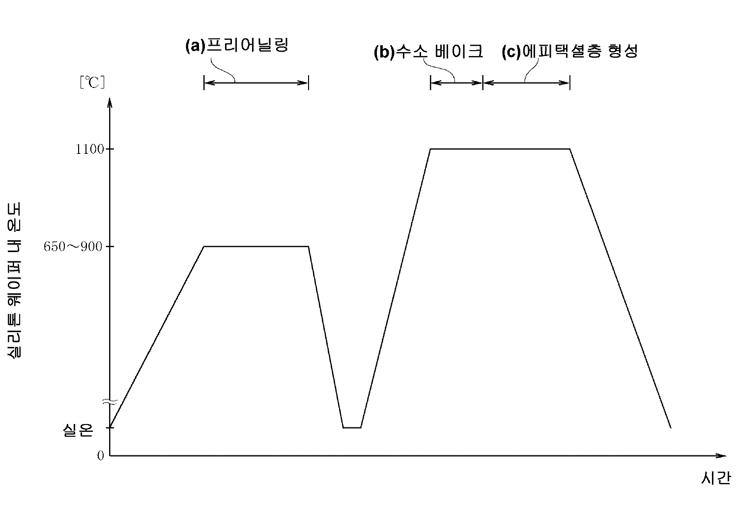
이와 같이 산소 석출 핵을 BMD로 성장시키기 위한 실리콘 웨이퍼의 프리 어닐링 공정의 순서를 개시한다. 도 1에 도시한 바와 같이, 프리 어닐링 공정에서는 식각이 실시된 후의 실온 하에 놓인 실리콘 웨이퍼를 로내 온도 600 내지 700℃의 저항 가열식 종형 로에 수용하고, 승온 속도 1 내지 8℃/분, 바람직하게는 4 내지 6℃/분으로 650 내지 900℃의 온도 범위 내의 소정의 온도까지 승온하고, 소정의 온도에서 10분 내지 4시간 , 바람직하게는 30 내지 60분 유지하고, 강온 속도 5 내지 2℃/분, 바람직하게는 4 내지 3℃/분으로 실온까지 냉각한다. 로내 분위기는 질소(N2) 가스, 아르곤 가스 또는 이들의 혼합 가스의 불활성 가스 분위기이다. Thus, the procedure of the pre-annealing process of a silicon wafer for growing an oxygen precipitation nucleus to BMD is described. As shown in Fig. 1, in the pre-annealing step, the silicon wafer placed at room temperature after etching is accommodated in a resistance heating vertical furnace having an internal furnace temperature of 600 to 700 ° C, and the temperature increase rate is 1 to 8 ° C / minute, preferably 4 To 6 deg. C / min to a predetermined temperature within a temperature range of 650 to 900 deg. C, held at a predetermined temperature for 10 minutes to 4 hours, preferably 30 to 60 minutes, and a temperature-fall rate of 5 to 2 deg. Preferably it is cooled to room temperature at 4 to 3 ° C / min. The furnace atmosphere is an inert gas atmosphere of nitrogen (N 2 ) gas, argon gas or a mixture of these.
프리 어닐링 공정이 끝난 실리콘 웨이퍼를 연마에 의해 광학적인 광택을 가진 경면 웨이퍼로 마감한다. 이와 같이 경면 연마에 의해 마감된 실리콘 웨이퍼의 표면 상에 에피택셜층을 성장시킨다. 예컨대, 실리콘 웨이퍼를 매엽식 에피택셜 장치에 수용하고, 장치 내 온도를 1000 내지 1150℃로 하고, 1분간의 수소 베이크를 행하고, 계속하여 트라이클로로실레인(trichlorosilane) 가스를 장치 내에 유입시켜 온도 1000 내지 1150℃에서 30 내지 180초간, 바람직하게는 60 내지 120초간 실리콘 웨이퍼를 유지함으로써 실리콘 웨이퍼 표면에 두께 4μm의 에피택셜층을 형성한다. 이에 따라 에피택셜층 표면에서 0.09μm 이상의 크기의 에피택셜 결함이 3개/장 이하인 밀도를 가지며, 에피택셜층을 제외한 웨이퍼 내부에 형성되는 BMD 밀도가 1×10⁴개/cm2 내지 5×10⁶개/cm2 이하인 에피택셜 웨이퍼를 얻을 수 있다. After the pre-annealing process, the silicon wafer is polished to a mirror wafer with optical gloss. The epitaxial layer is grown on the surface of the silicon wafer finished by mirror polishing. For example, the silicon wafer is housed in a single wafer epitaxial device, the temperature in the device is 1000 to 1150 ° C., hydrogen baking is performed for 1 minute, and trichlorosilane gas is then introduced into the device to obtain a temperature of 1000. An epitaxial layer having a thickness of 4 μm is formed on the surface of the silicon wafer by holding the silicon wafer at from 1150 ° C. for 30 to 180 seconds, preferably 60 to 120 seconds. Accordingly, the epitaxial layer has a density of three epitaxial defects of 0.09 μm or more on the surface of the epitaxial layer, and has a density of 1 × 10 4 pcs / cm 2 to 5 × 10 formed inside the wafer excluding the epitaxial layer. 6 pcs / cm 2 The following epitaxial wafers can be obtained.
<제2 실시 형태><2nd embodiment>
다음, 본 발명을 실시하기 위한 제2 실시 형태를 설명한다. 본 발명의 에피택셜 실리콘 웨이퍼의 제조 방법은 CZ법에 의해 보론이 첨가된 실리콘 융액(11)으로부터 직경 300mm의 실리콘 단결정(12)을 챔버(21) 내에서 강제 냉각하여 챔버(21) 내에서 CZ법에 의해 인상시키는 공정과, 이 단결정을 슬라이스하여 얻어진 실리콘 웨이퍼의 표면에 에피택셜층을 형성하는 공정을 포함한다. 즉, 이 제2 실시 형태에서는 도 3에 도시한 바와 같이, 강제 냉각은 챔버(21) 내에 설치된 수냉식 냉각 장치(36)에 의해 행해진다. 그리고, 실리콘 단결정(12)은 인상 도중의 800 내지 600℃의 온도 영역을 냉각 장치(36)의 내부에 설치된 냉각용 통체(37)의 내부를 180분 미만 120분 이상으로 통과하여 육성된다. 그 육성된 실리콘 단결정(12)은 산소 농도 10×1017 내지 14×1017atoms/cm3 및 저항률 0.03 내지 0.01Ωcm를 갖는다. 실리콘 단결정(12)은 직경 300mm 이상인 것이 바람직하며, 직경 300 내지 450mm인 것이 더욱 바람직하다 이 단결정으로부터 슬라이스하여 얻어진 실리콘 웨이퍼의 표면에 에피택셜층을 형성하기 전에 실리콘 웨이퍼를 불활성 가스 분위기 하 650 내지 900℃의 온도 범위 내의 소정의 온도에서 10분 내지 4시간 유지하는 프리 어닐링이 행해진다. 프리 어닐링에 있어서, 실온에서부터의 승온 속도 및 실온까지의 강온 속도는 제1 실시 형태와 동일하다. Next, 2nd Embodiment for implementing this invention is demonstrated. In the method for manufacturing an epitaxial silicon wafer of the present invention, the silicon
본 발명에 있어서, 인상 도중의 800 내지 600℃의 온도 영역의 통과 시간을 180분 미만 120분 이상으로 설정한 것은, 120분 이상으로 함으로써 단결정(2) 내부에 형성되는 BMD 밀도를 증가시킬 수 있기 때문이다. 또한, 챔버(21) 내에 냉각 장치를 설치함으로써 단결정(2)의 통과 시간을 180분 미만 120분 이상으로 할 수 있다. 또한, 통과 시간이 180분 미만 120분 이상으로 더욱 단시간에 냉각시킴으로써 제1 실시 형태에 비하여 그 생산성이 보다 높아진다. In the present invention, setting the passage time in the temperature range of 800 to 600 ° C. during the pulling up to less than 180 minutes to 120 minutes or more can increase the BMD density formed inside the single crystal 2 by setting it to 120 minutes or more. Because. Moreover, by providing a cooling device in the
나아가, 산소 농도의 프로세스 마진을 10×1017 내지 14×1017atoms/cm3로 크게 설정한 것은, 인상 도중의 800 내지 600℃의 온도 영역을 180분 미만 120분 이상에 걸쳐 통과시킴으로써 과잉의 산소 석출 핵의 형성을 억제하기 때문이다. 이에 따라, 고농도의 보론이 첨가된 저항률 0.03 내지 0.01Ωcm를 갖는 실리콘 단결정(12)이라도, 그리고 산소 농도가 높아도 산소 석출 과다로 인한 BMD에 기인하는 에피택셜 결함이 발생하는 것을 방지할 수 있다. 또한, 산소 농도의 프로세스 마진을 크게 함으로써 실리콘 단결정(12)을 양산함에 있어서 산소 농도, 비저항 등의 프로세스 특성이 다소 흔들려도 불량품의 발생률을 저감할 수 있다. Furthermore, setting the process margin of oxygen concentration large at 10 × 10 17 to 14 × 10 17 atoms / cm 3 is excessive by passing the temperature range of 800 to 600 ° C. during the pulling over less than 180 minutes to 120 minutes or more. This is because the formation of oxygen precipitate nuclei is suppressed. As a result, even in the silicon
다음, 본 발명의 실시예를 비교예와 함께 설명한다. Next, the Example of this invention is described with a comparative example.
<실시예 1><Example 1>
실리콘 단결정을 육성하는 CZ로(10)를 도 2에 도시하였다. 구체적으로는, 메인 챔버(21) 내의 중심 위치에 실리콘 융액(11)을 저장하는 도가니(22)가 설치된다. 도가니(22)는 석영으로 이루어지는 용기(22a)와 이 외측에 배치된 흑연으로 이루어지는 용기(22b)로 구성되며, 지축(23)을 통하여 도가니(22)를 회전시키고 승강시키는 도가니 구동 수단(24)에 접속된다. 도가니(22)의 외주부에는 가열 히터(25)와 보온통(26)이 동심원상으로 배치된다. 도가니(22) 내에는 실리콘 단결정이 가열 히터(25)에 의해 융해된 실리콘 융액(11)이 수용된다. A
메인 챔버(21)의 상단에는 원통형의 풀 챔버(27)가 접속되며, 이 풀 챔버(27)의 상단에는 시드 인상 수단(도시 생략)이 설치되고, 와이어 케이블(28)이 시드 결정(29)을 장착하여 회전 및 승강 가능하게 설치되어 있다. 이 시드 결정(29)의 하단으로부터 단결정(12)을 성장시키는 것이 가능하고, 더욱이 와이어 케이블(28)이 상승함과 아울러 육성되는 단결정(12)을 둘러싸도록 열 차폐 부재(30)가 배치된다. 열 차폐 부재(30)는 하방을 향함에 따라 지름이 작아지는 콘부(30a)와, 콘부에 연속되어 설치되며 외방으로 튀어나오는 플랜지부(30b)와, 플랜지부(30b)를 보온통(26) 상에 올려놓기 위한 링판(30c)으로 구성되어 있다. A cylindrical
또한, 풀 챔버(27) 및 메인 챔버(21) 내에는 아르곤 가스 등의 불활성 가스가 공급 가스 유량 조정 밸브(31)를 갖는 가스 공급 파이프(32)와 배출 가스 유량 조절 밸브(33)를 갖는 가스 배출 파이프(34)를 지남으로써 유통되도록 구성된다. 더욱이, 메인 챔버(21)의 외측의 좌우에는 자계 인가 장치(35)가 배치되며, 실리콘 융액(11)의 대류를 제어한다. Further, in the
이 CZ로(10)를 이용하여 보론이 첨가된 실리콘 융액(11)으로부터 실리콘 단결정(12)을 불활성 가스를 캐리어 가스로 하여 챔버(21) 내에 흘리면서 0.95mm/분의 속도로 인상시키고, 그 인상 도중의 800 내지 600℃의 온도 영역을 182분에 걸 쳐 통과시켜 그 단결정을 육성하였다. 도가니(22)의 회전 속도와 MCZ(Magnetic field applied CZ)법의 자계 인가 장치(35)에 의해 자기장 강도를 조정하고, 아르곤 가스의 유속과 CZ로(10) 내의 압력을 조정함으로써 실리콘 단결정(12)에 포함되는 산소 농도를 제어하였다. 이 단결정을 슬라이스하여 얻어진 실리콘 웨이퍼의 저항률 및 산소 농도를 4탐침법 및 이차 이온 질량 분석법(SIMS)을 이용하여 각각 계측하였더니, 실리콘 단결정(12)의 저항률은 0.03 내지 0.01Ωcm, 산소 농도가 10.05×10¹⁷atoms/cm3이었다. By using this
화학 식각하여 얻어진 상기 실리콘 웨이퍼를 650℃로 가열한 종형 로에 수용하였다. 질소 가스 분위기 하에서, 이 종형 로의 로내 온도를 650℃에서부터 승온 속도 5℃/분으로 850℃까지 승온하고, 이 온도에서 실리콘 웨이퍼를 1시간 유지하고, 강온 속도 3℃/분으로 실온까지 냉각하는 프리 어닐링 처리를 실시하였다. 이 실리콘 웨이퍼에 경면 연마를 실시한 후, 매엽식 에피택셜 장치에 수용하고, 장치 내 온도를 1100℃, 1분간의 수소 베이크 처리를 실리콘 웨이퍼에 행하고, 계속하여 트라이클로로실레인 가스를 장치 내에 유입시키고 장치 내 온도 1100℃, 120초간 유지함으로써 실리콘 웨이퍼 표면에 두께 4μm의 에피택셜층을 형성하였다. 이에 따라 에피택셜 웨이퍼를 얻었다. 얻어진 에피택셜 웨이퍼를 실시예 1로 하였다. The silicon wafer obtained by chemical etching was accommodated in a vertical furnace heated to 650 ° C. In a nitrogen gas atmosphere, the furnace temperature of the vertical furnace is increased from 650 ° C to 850 ° C at a heating rate of 5 ° C / min, and the silicon wafer is held at this temperature for 1 hour, and the freezer is cooled to room temperature at a temperature-fall rate of 3 ° C / min. Annealing treatment was performed. After performing mirror polishing on this silicon wafer, it was accommodated in a single wafer type epitaxial device, hydrogenated at 1100 ° C. for 1 minute with hydrogen baking treatment on the silicon wafer, and then trichlorosilane gas was introduced into the device. An epitaxial layer having a thickness of 4 μm was formed on the surface of the silicon wafer by maintaining the internal temperature of the device at 1100 ° C. for 120 seconds. This obtained an epitaxial wafer. The obtained epitaxial wafer was used as Example 1.
<실시예 2 내지 6><Examples 2 to 6>
실리콘 단결정의 육성에 있어서 실리콘 단결정(12)의 800 내지 600℃의 온도 영역을 통과하는 시간을, 인상 속도를 0.85 내지 0.95mm/분으로 바꿈으로써 표 1에 나타낸 바와 같이 250분 이하 180분 이상의 범위 내로 변경하였다. 또한, 도가니(22)의 회전 속도와 자계 인가 장치(35)에 의해 자계 강도를 변경하고, 아르곤 가스의 유속과 CZ로(10) 내의 압력을 조정함으로써 실리콘 단결정(12)에 포함되는 산소 농도를 표 1에 나타낸 바와 같이 10×1017 내지 12×1017atoms/cm3의 범위 내에서 변경하였다. 상기 변경을 제외하고 실시예 1과 동일한 방법으로 각각 에피택셜 웨이퍼를 얻었다. 얻어진 에피택셜 웨이퍼를 각각 실시예 2 내지 6으로 하였다. In the growth of the silicon single crystal, the time passing through the temperature range of 800 to 600 ° C. of the silicon
<비교예 1 내지 6><Comparative Examples 1 to 6>
실리콘 단결정의 육성에 있어서 실리콘 단결정(12)의 800 내지 600℃의 온도 영역을 통과하는 시간을, 인상 속도를 0.85 내지 0.95mm/분으로 바꿈으로써 표 1에 나타낸 바와 같이 250분 이하 180분 이상의 범위 내로 변경하였다. 또한, 도가니(22)의 회전 속도와 자계 인가 장치(35)에 의해 자계 강도를 변경하고, 아르곤 가스의 유속과 CZ로(10) 내의 압력을 조정함으로써 실리콘 단결정(12)에 포함되는 산소 농도를 표 1에 나타낸 바와 같이 10×1017 내지 12×1017atoms/cm3의 범위 밖에서 변경하였다. 상기 변경을 제외하고 실시예 1과 동일한 방법으로 각각 에피택셜 웨이퍼를 얻었다. 얻어진 에피택셜 웨이퍼를 각각 비교예 1 내지 6으로 하였다. In the growth of the silicon single crystal, the time passing through the temperature range of 800 to 600 ° C. of the silicon
<비교예 7 내지 10><Comparative Examples 7 to 10>
실리콘 단결정의 육성에 있어서 실리콘 단결정(12)의 800 내지 600℃의 온도 영역을 통과하는 시간을, 인상 속도를 0.75/분으로 바꿈으로서 표 1에 나타낸 바와 같이 250분 이하 180분 이상의 범위 밖으로 변경하였다. 또한, 도가니(22)의 회전 속도와 자계 인가 장치(35)에 의해 자계 강도를 변경하고, 아르곤 가스의 유속과 CZ로(10) 내의 압력을 조정함으로써 실리콘 단결정(12)에 포함되는 산소 농도를 표 1에 나타낸 바와 같이 변경하였다. 상기 변경을 제외하고 실시예 1과 동일한 방법으로 각각 에피택셜 웨이퍼를 얻었다. 얻어진 에피택셜 웨이퍼를 각각 비교예 7 내지 10으로 하였다. In the growth of the silicon single crystal, the time passing through the 800 to 600 ° C. temperature range of the silicon
<비교예 11 내지 22><Comparative Examples 11 to 22>
실리콘 단결정의 육성에 있어서 실리콘 단결정(12)의 800 내지 600℃의 온도 영역을 통과하는 시간을, 인상 속도를 0.85 내지 0.95mm/분으로 바꿈으로써 표 2에 나타낸 바와 같이 250분 이하 180분 이상의 범위 내로 변경하였다. 또한, 도가니(22)의 회전 속도와 자계 인가 장치(35)에 의해 자계 강도를 변경하고, 아르곤 가스의 유속과 CZ로(10) 내의 압력을 조정함으로써 실리콘 단결정(12)에 포함되는 산소 농도를 표 2에 나타낸 바와 같이 변경하였다. 더욱이 프리 어닐링 공정을 행하지 않고 에피택셜층을 형성하였다. 상기 변경을 제외하고 실시예 1과 동일한 방법으로 각각 에피택셜 웨이퍼를 얻었다. 얻어진 에피택셜 웨이퍼를 각각 비교예 11 내지 22로 하였다. In the growth of the silicon single crystal, the time passing through the temperature range of 800 to 600 ° C. of the silicon
<비교예 23 내지 26><Comparative Examples 23 to 26>
실리콘 단결정의 육성에 있어서 실리콘 단결정(12)의 800 내지 600℃의 온도 영역을 통과하는 시간을, 인상 속도를 0.75 내지 1.05mm/분으로 바꿈으로써 표 2에 나타낸 바와 같이 250분 이하 180분 이상의 범위 밖으로 변경하였다. 또한, 도가니(22)의 회전 속도와 자계 인가 장치(35)에 의해 자계 강도를 변경하고, 아르곤 가스의 유속과 CZ로(10) 내의 압력을 조정함으로써 실리콘 단결정(12)에 포함되는 산소 농도를 표 2에 나타낸 바와 같이 변경하였다. 더욱이 프리 어닐링 공정을 행하지 않고 에피택셜층을 형성하였다. 상기 변경을 제외하고 실시예 1과 동일한 방법으로 각각 에피택셜 웨이퍼를 얻었다. 얻어진 에피택셜 웨이퍼를 각각 비교예 23 내지 26으로 하였다. In the growth of the silicon single crystal, the time passing through the temperature range of 800 to 600 ° C. of the silicon
<비교 시험 1>Comparative Test 1
실시예1 내지 6, 및 비교예 1 내지 26의 에피택셜 실리콘 웨이퍼를 표면 결함 검사 장치(KLA-Tencor사 제품; SP-1)를 이용하여 에피택셜층의 표면에서 검출되는 0.09μm 이상의 크기의 표면 결함(에피택셜 결함)의 수를 측정하였다. 다음, 이들 에피택셜 웨이퍼에 대하여 건조 산소 분위기 중 l000℃에서 16시간 유지하여 BMD 성장 열처리를 실시한 후, 에피택셜 웨이퍼를 벽개하여 벽개 단면을 라이트 식각액으로 2μm의 선택 식각을 행하고, 이 벽개 단면을 광학 현미경을 이용하여 식각 피트(에치 피트) 밀도를 측정하고, 실리콘 웨이퍼 중에 형성된 산소 석출물(BMD) 밀도를 구하였다. 이들 측정 결과를 표 1 및 표 2에 나타내었다. Surfaces of a size of 0.09 μm or more, wherein the epitaxial silicon wafers of Examples 1 to 6 and Comparative Examples 1 to 26 were detected on the surface of the epitaxial layer using a surface defect inspection apparatus (manufactured by KLA-Tencor; SP-1) The number of defects (epitaxial defects) was measured. Next, these epitaxial wafers were subjected to BMD growth heat treatment by holding them at l000 ° C for 16 hours in a dry oxygen atmosphere, and then cleaving the epitaxial wafers to selectively etch the cleaved cross section with a light etchant to 2 μm. The etching pit (etch pit) density was measured using a microscope, and the density of oxygen precipitates (BMD) formed in the silicon wafer was obtained. These measurement results are shown in Table 1 and Table 2.


<평가 1><Evaluation 1>
표 1 및 표 2의 웨이퍼 1장 당 에피택셜 결함의 개수는 3000장의 에피택셜 웨이퍼를 측정한 평균값을 나타내고 있다. 표 1 및 표 2에서 알 수 있는 바와 같이, 웨이퍼 1장 당 에피택셜 결함 개수의 평균값은 실시예 1 내지 6 및 비교예 1, 비교예 3, 비교예 5, 비교예 11 내지 25에서는 3개 이하로 낮은 수치를 나타내었고, 비교예 7 내지 8, 비교예 26에서는 50개 이상, 비교예 2, 비교예 4, 비교예 6, 비교예 9 내지 10에서는 100개 이상으로 높은 수치를 나타내었다. The number of epitaxial defects per wafer of Table 1 and Table 2 has shown the average value which measured 3000 epitaxial wafers. As can be seen from Table 1 and Table 2, the average value of the number of epitaxial defects per wafer is three or less in Examples 1 to 6 and Comparative Examples 1 and 3, Comparative Examples 5 and 11 to 25. In the comparative examples 7 to 8 and the comparative example 26, the numerical value was low, and the numerical value was as high as 100 or more in the comparative example 2, the comparative example 4, the comparative example 6, and the comparative examples 9-10.
또한 BMD 밀도는 실시예 1 내지 6 및 비교예 2, 비교예 4, 비교예 6 내지 10, 비교예 26에서는 1×10⁴개/cm2 이상으로 높은 수치를 나타내었고, 비교예 1, 비교예 3, 비교예 5, 비교예 11 내지 25에서는 1×10⁴개/cm2 미만으로 낮은 수치를 나타내었다.In addition, the BMD density is 1 × 10 4 pcs / cm 2 in Examples 1 to 6 and Comparative Examples 2, 4, 6 to 10, and Comparative Example 26. The numerical values were as high as above, and in Comparative Example 1, Comparative Example 3, Comparative Example 5, and Comparative Examples 11 to 25, 1 × 10 4 pieces / cm 2 Low values were shown below.
이상으로부터, 에피택셜 결함의 개수의 평균값에 대해서는, 산소 농도가 12×1017atoms/cm3를 초과하는 높은 농도 그리고 프리 어닐링 처리를 실시함으로써 증가하기 때문에 산소 농도의 상한을 12×1017atoms/cm3 이하로 하는 것이 좋음을 알 수 있었다. BMD 밀도에 대해서는, 프리 어닐링 처리를 실시한 예가 프리 어닐링 처리를 실시하지 않은 예보다 밀도가 높아졌기 때문에 프리 어닐링 처리를 하는 것이 좋음을 알 수 있었다. 또한, 통과 시간이 180 내지 250분의 범위에 들어가 있음에도 불구하고 BMD 밀도가 1×10⁴개/cm2 미만으로 되어 버리는 비교예 1, 비교예 3, 비교예 5가 있어, 이것을 피하기 위하여 산소 농도의 하한값을 10×1017atoms/cm3 이상으로 하는 것이 좋음을 알 수 있었다. As mentioned above, about the average value of the number of epitaxial defects, since the oxygen concentration increases by carrying out the high concentration exceeding 12 * 10 <17> atoms / cm < 3 > and a pre-annealing process, the upper limit of oxygen concentration is 12 * 10 <17> atoms / cm 3 It turned out that it is good to set it as follows. As for the BMD density, it was found that the preannealing treatment was better because the example of the preannealing treatment was higher in density than the example without the preannealing treatment. In addition, there is Comparative Example 1, Comparative Example 3, and Comparative Example 5 in which the BMD density becomes less than 1 × 10 4 pieces / cm 2 even though the passage time is in the range of 180 to 250 minutes. It turned out that it is good to set the lower limit of to 10x10 17 atoms / cm 3 or more.
상기 실시예 1 내지 6 및 비교예 1 내지 26의 결과로부터, 800 내지 600℃의 온도 영역을 250 내지 180분에 걸쳐 통과시켜 육성되고, 산소 농도10 내지 12×1017atoms/cm3를 갖는 실리콘 단결정(12)으로부터 얻어진 실리콘 웨이퍼에 에피택셜층 형성 전에 프리 어닐링 처리를 함으로써 게터링에 유효한 BMD 밀도가 1×10⁴개/cm2 이상으로 높고 에피택셜 결함 개수가 1장 당 3개 이하로 적은 에피택셜 웨이퍼를 제조할 수 있음을 알 수 있었다.From the results of the above Examples 1 to 6 and Comparative Examples 1 to 26, silicon was grown by passing a temperature range of 800 to 600 ° C. over 250 to 180 minutes and having an oxygen concentration of 10 to 12 × 10 17 atoms / cm 3 . By pre-annealing the silicon wafer obtained from the
<실시예 7><Example 7>
실리콘 단결정을 육성하는 CZ로(20)를 도 3에 도시하였다. 도 3에서 도 2와 동일 부호는 동일 구성 요소를 나타내며, 제1 실시 형태와 대략 동일하므로 반복 설명을 생략한다. 메인 챔버(21) 내에는 냉각 장치(36)가 육성되는 단결정(12)을 둘러싸도록 설치된다. 냉각 장치(36)의 내부에는 냉각 수로(37a)를 갖는 냉각용 통체(37)와, 냉각 수로(37a)에 연통 접속되며 챔버(21) 바깥에서 냉각 수로(37a)로 냉각수를 소정의 압력으로 공급하는 공급관(38)과, 냉각 수로(37a)에 연통 접속되며 챔버(21) 바깥으로 냉각 수로(37a)의 냉각수를 배출하는 배출관(39)을 구비한다. A CZ furnace 20 for growing a silicon single crystal is shown in FIG. In FIG. 3, the same code | symbol as FIG. 2 shows the same component, and since it is substantially the same as 1st Embodiment, repeated description is abbreviate | omitted. The
이 CZ로(20)를 이용하여 보론이 첨가된 실리콘 융액(11)으로부터 실리콘 단결정(12)을 불활성 가스를 캐리어 가스로 하여 챔버(21) 내에 흘리면서 1.3mm/분의 속도로 인상시키고, 그 인상 도중의 800 내지 600℃의 온도 영역을 120분에 걸쳐 통과시켜 그 단결정을 육성하였다. 도가니(22)의 회전 속도와 자계 인가 장치(35)에 의해 자계 강도를 조정하고, 아르곤 가스의 유속과 CZ로(20) 내의 압력을 조정함으로써 실리콘 단결정(12)에 포함되는 산소 농도를 제어하였다. 이 단결정을 슬라이스하여 얻어진 실리콘 웨이퍼의 저항률 및 산소 농도를 4탐침법 및 이차 이온 질량 분석법(SIMS)을 이용하여 각각 계측하였더니, 실리콘 단결정(12)의 저항률은 0.03 내지 0.01Ωcm, 산소 농도가 10.22×10¹⁷atoms/cm3이었다. Using this CZ furnace 20, the silicon
화학 식각하여 얻어진 상기 실리콘 웨이퍼를 650℃로 가열한 종형 로에 수용하였다. 질소 가스 분위기 하에서, 이 종형 로의 로내 온도를 650℃에서부터 승온 속도 5℃/분으로 850℃까지 승온하고, 이 온도에서 실리콘 웨이퍼를 1시간 유지하고, 강온 속도 3℃/분으로 실온까지 냉각하는 프리 어닐링 처리를 실시하였다. 이 실리콘 웨이퍼에 경면 연마를 실시한 후, 매엽식 에피택셜 장치에 수용하고, 장치 내 온도를 1100℃, 1분간의 수소 베이크 처리를 실리콘 웨이퍼에 행하고, 계속하여 트라이클로로실레인 가스를 장치 내에 유입시켜 장치 내 온도 1100℃, 120초간 유지함으로써 실리콘 웨이퍼 표면에 두께 4μm의 에피택셜층을 형성하였다. 이에 따라 에피택셜 웨이퍼를 얻었다. 얻어진 에피택셜 웨이퍼를 실시예 7로 하였다. The silicon wafer obtained by chemical etching was accommodated in a vertical furnace heated to 650 ° C. In a nitrogen gas atmosphere, the furnace temperature of the vertical furnace is increased from 650 ° C to 850 ° C at a heating rate of 5 ° C / min, and the silicon wafer is held at this temperature for 1 hour, and the freezer is cooled to room temperature at a temperature-fall rate of 3 ° C / min. Annealing treatment was performed. After performing mirror polishing on this silicon wafer, it was accommodated in a single wafer type epitaxial device, hydrogenated for 1 minute at 1100 ° C. and subjected to hydrogen baking on the silicon wafer, and then trichlorosilane gas was introduced into the device. An epitaxial layer having a thickness of 4 μm was formed on the surface of the silicon wafer by maintaining the internal temperature of the device at 1100 ° C. for 120 seconds. This obtained an epitaxial wafer. The obtained epitaxial wafer was used as Example 7.
<실시예 8 내지 12><Examples 8 to 12>
실리콘 단결정의 육성에 있어서 실리콘 단결정(12)의 800 내지 600℃의 온도 영역을 통과하는 시간을, 인상 속도를 1.3 내지 1.0mm/분으로 바꿈으로써 표 3에 나타낸 바와 같이 180분 미만 120분 이상의 범위 내로 변경하였다. 또한, 도가니(22)의 회전 속도와 자계 인가 장치(35)에 의해 자계 강도를 변경하고, 아르곤 가스의 유속과 CZ로(20) 내의 압력을 조정함으로써 실리콘 단결정(12)에 포함되는 산소 농도를 표 3에 나타낸 바와 같이 변경하였다. 상기 변경을 제외하고 실시예 7과 동일한 방법으로 각각 에피택셜 웨이퍼를 얻었다. 얻어진 에피택셜 웨이퍼를 각각 실시예 8 내지 12로 하였다. In the growth of the silicon single crystal, the time passing through the temperature range of 800 to 600 ° C. of the silicon
<비교예 27 내지 32><Comparative Examples 27 to 32>
실리콘 단결정의 육성에 있어서 실리콘 단결정(12)의 800 내지 600℃의 온도 영역을 통과하는 시간을, 인상 속도를 1.3 내지 1.0mm/분으로 바꿈으로써 표 3에 나타낸 바와 같이 180분 미만 120분 이상의 범위 내로 변경하였다. 또한, 도가니(22)의 회전 속도와 자계 인가 장치(35)에 의해 자계 강도를 변경하고, 아르곤 가스의 유속과 CZ로(20) 내의 압력을 조정함으로써 실리콘 단결정(12)에 포함되는 산소 농도를 표 3에 나타낸 바와 같이 변경하였다. 상기 변경을 제외하고 실시예 7과 동일한 방법으로 각각 에피택셜 웨이퍼를 얻었다. 얻어진 에피택셜 웨이퍼를 각각 비교예 27 내지 32로 하였다. In the growth of the silicon single crystal, the time passing through the temperature range of 800 to 600 ° C. of the silicon
<비교예 33 내지 36><Comparative Examples 33 to 36>
실리콘 단결정의 육성에 있어서 실리콘 단결정(12)의 800 내지 600℃의 온도 영역을 통과하는 시간을, 인상 속도를 1.4mm/분으로 바꿈으로써 표 3에 나타낸 바와 같이 180분 미만 120분 이상의 범위 밖으로 변경하였다. 또한, 도가니(22)의 회전 속도와 자계 인가 장치(35)에 의해 자계 강도를 변경하고, 아르곤 가스의 유속과 CZ로(20) 내의 압력을 조정함으로써 실리콘 단결정(12)에 포함되는 산소 농도를 표 3에 나타낸 바와 같이 변경하였다. 상기 변경을 제외하고 실시예 7과 동일한 방법으로 각각 에피택셜 웨이퍼를 얻었다. 얻어진 에피택셜 웨이퍼를 각각 비교예 33 내지 36으로 하였다. In the growth of the silicon single crystal, the time passing through the temperature range of 800 to 600 ° C. of the silicon
<비교예 37 내지 42><Comparative Examples 37 to 42>
실리콘 단결정의 육성에 있어서 실리콘 단결정(12)의 800 내지 600℃의 온도 영역을 통과하는 시간을, 인상 속도를 1.3 내지 1.0mm/분으로 바꿈으로써 표 4에 나타낸 바와 같이 180분 미만 120분 이상의 범위 내로 변경하였다. 또한, 도가니(22)의 회전 속도와 자계 인가 장치(35)에 의해 자계 강도를 변경하고, 아르곤 가스의 유속과 CZ로(20) 내의 압력을 조정함으로써 실리콘 단결정(12)에 포함되는 산소 농도를 표 4에 나타낸 바와 같이 변경하였다. 더욱이 프리 어닐링 공정을 행하지 않고 에피택셜층을 형성하였다. 상기 변경을 제외하고 실시예 7과 동일한 방법으로 각각 에피택셜 웨이퍼를 얻었다. 얻어진 에피택셜 웨이퍼를 각각 비교예 37 내지 42로 하였다. In the growth of the silicon single crystal, the time passing through the temperature range of 800 to 600 ° C. of the silicon
<비교예 43 내지 48><Comparative Examples 43 to 48>
실리콘 단결정의 육성에 있어서 실리콘 단결정(12)의 800 내지 600℃의 온도 영역을 통과하는 시간을, 인상 속도를 1.3 내지 1.0mm/분으로 바꿈으로써 표 4에 나타낸 바와 같이 180분 미만 120분 이상의 범위 내로 변경하였다. 또한, 도가니(22)의 회전 속도와 자계 인가 장치(35)에 의해 자계 강도를 변경하고, 아르곤 가스의 유속과 CZ로(20) 내의 압력을 조정함으로써 실리콘 단결정(12)에 포함되는 산소 농도를 표 4에 나타낸 바와 같이 변경하였다. 더욱이 프리 어닐링 공정을 행하지 않고 에피택셜층을 형성하였다. 상기 변경을 제외하고 실시예 7과 동일한 방법으로 각각 에피택셜 웨이퍼를 얻었다. 얻어진 에피택셜 웨이퍼를 각각 비교예 43 내지 48로 하였다. In the growth of the silicon single crystal, the time passing through the temperature range of 800 to 600 ° C. of the silicon
<비교예 49 내지 52><Comparative Examples 49 to 52>
실리콘 단결정의 육성에 있어서 실리콘 단결정(12)의 800 내지 600℃의 온도 영역을 통과하는 시간을, 인상 속도를 1.4mm/분으로 바꿈으로써 표 4에 나타낸 바와 같이 180분 미만 120분 이상의 범위 밖으로 변경하였다. 또한, 도가니(22)의 회전 속도와 자계 인가 장치(35)에 의해 자계 강도를 변경하고, 아르곤 가스의 유속과 CZ로(20) 내의 압력을 조정함으로써 실리콘 단결정(12)에 포함되는 산소 농도를 표 4에 나타낸 바와 같이 변경하였다. 더욱이 프리 어닐링 공정을 행하지 않고 에피택셜층을 형성하였다. 상기 변경을 제외하고 실시예 7과 동일한 방법으로 각각 에피택셜 웨이퍼를 얻었다. 얻어진 에피택셜 웨이퍼를 각각 비교예 49 내지 52로 하였다. In the growth of the silicon single crystal, the time passing through the temperature range of 800 to 600 ° C. of the silicon


<평가 2><Evaluation 2>
표 3 및 표4의 웨이퍼 1장 당 에피택셜 결함의 개수는 3000장의 에피택셜 웨이퍼를 측정한 평균값을 나타내고 있다. 표 3 및 표4에서 알 수 있는 바와 같이, 웨이퍼 1장 당 에피택셜 결함 개수의 평균값은 실시예 7 내지 12에서는 3개 이하로 낮은 값을 나타내었고, BMD 밀도도 1×10⁴개/cm2 이상의 높은 수치를 나타내었다. The number of epitaxial defects per wafer of Table 3 and Table 4 has shown the average value which measured 3000 epitaxial wafers. As can be seen from Table 3 and Table 4, the average value of the number of epitaxial defects per wafer was as low as 3 or less in Examples 7 to 12, the BMD density is also 1 × 10 4 / cm 2 The high value was shown.
이상으로부터, 에피택셜 결함의 개수의 평균값에 대해서는, 냉각 장치를 설치한 경우에도 산소 농도가 14×1017atoms/cm3를 초과하는 높은 농도의 경우 프리 어닐링에 의해 증가하기 때문에 산소 농도의 상한을 14×1017atoms/cm3 이하로 하는 것이 좋음을 알 수 있었다. BMD 밀도에 대해서는, 산소 농도가 10×1017atoms/cm3 미만인 경우 1×10⁴개/cm2 미만이 되어 프리 어닐링 처리를 실시한 예가 프리 어닐링 처리를 실시하지 않은 예보다 밀도가 높아졌기 때문에, 프리 어닐링 처리를 하는 것이 좋음을 알 수 있었다. 또한, 통과 시간이 120 내지 180분의 범위에 들어가 있음에도 불구하고 BMD 밀도가 1×10⁴개/cm2 미만으로 되어 버리는 비교예 27, 29, 31이 있어, 이것을 피하기 위하여 산소 농도의 하한값을 10×1017atoms/cm3 이상으로 하는 것이 좋음을 알 수 있었다. In view of the above, the average value of the number of epitaxial defects is increased by pre-annealing when the oxygen concentration is higher than 14 x 10 17 atoms / cm 3 even when a cooling device is provided. 14 × 10 17 atoms / cm 3 It turned out that it is good to set it as follows. About the BMD density, 1 × 10 4 pieces / cm 2 when the oxygen concentration is less than 10 × 10 17 atoms / cm 3 Since the density which became less than the example which performed the pre-annealing process became higher than the example which did not perform the pre-annealing process, it turned out that it is preferable to perform a pre-annealing process. In addition, the BMD density is 1 × 10 4 pcs / cm 2 , although the transit time is in the range of 120 to 180 minutes. There are comparative examples 27, 29, and 31 which become less than, and in order to avoid this, the lower limit of the oxygen concentration is 10 × 10 17 atoms / cm 3 It turned out that it is good to make more than that.
상기 실시예 7 내지 12 및 비교예 27 내지 52의 결과로부터, 챔버(21) 내에 냉각 장치(36)를 설치하고, 냉각 장치(36)의 내부에 설치된 냉각용 통체(37)를 통하여 챔버(21) 내의 인상 도중의 800 내지 600℃의 온도 영역을 180 내지 120분에 걸쳐 통과시켜 육성되고, 산소 농도 10 내지 14×1017atoms/cm3를 갖는 실리콘 단결정(12)으로부터 얻어진 실리콘 웨이퍼에 에피택셜층 형성 전에 프리 어닐링 처리를 실시함으로써 게터링에 유효한 BMD 밀도가 1×10⁴개/cm2 이상으로 높고, 에피택셜 결함 개수가 1장 당 3개 이하로 적은 에피택셜 웨이퍼를 제조할 수 있음을 알 수 있었다. From the result of the said Example 7-12 and Comparative Examples 27-52, the
또한, 통과 시간이 250분 이하 180분 이상인 실시예 1 내지 6에 비하여 통과 시간이 180분 미만 120분 이상인 실시예 7 내지 12는 IG 효과에 차이가 없으며, 통과 시간이 짧기 때문에 더욱 생산성을 향상시킬 수 있다. 또한, 800 내지 600℃의 온도 영역을 120분 이하로 통과시키는 조건에서는 비교예 35, 36, 51, 52에서 실시예와 동등한 품질이 얻어짐을 알 수 있었다. 그러나, 너무 빠른 속도로 단결정의 인상을 행하면 결정의 축 끊김, 갈라짐의 문제가 발생하게 되어 생산 효율이 나빠지므로 120분 이하의 적용은 행하지 않도록 하였다. In addition, Examples 7 to 12 having a passage time of less than 180 minutes and 120 minutes or more compared to Examples 1 to 6 having a passage time of 250 minutes or less and 180 minutes or more, have no difference in IG effect, and further improve productivity because of a short passage time. Can be. Moreover, it turned out that the quality equivalent to an Example was obtained by the comparative example 35, 36, 51, 52 on the conditions which let the temperature range 800-600 degreeC pass for 120 minutes or less. However, if the single crystal is pulled up too fast, problems such as axial breakage and cracking of the crystal may occur, resulting in poor production efficiency.
도 1은 본 발명 실리콘 웨이퍼의 열처리 시간과 온도 프로파일과의 관계를 보인 그래프이다. 1 is a graph showing a relationship between a heat treatment time and a temperature profile of a silicon wafer of the present invention.
도 2는 본 발명의 제1 실시 형태의 CZ로를 도시한 종단면 구성도이다. It is a longitudinal cross-sectional view which shows the CZ furnace of 1st Embodiment of this invention.
도 3은 본 발명의 제2 실시 형태의 CZ로를 도시한 종단면 구성도이다. It is a longitudinal cross-sectional block diagram which shows the CZ furnace of 2nd Embodiment of this invention.
Claims (7)
Applications Claiming Priority (2)
| Application Number | Priority Date | Filing Date | Title |
|---|---|---|---|
| JPJP-P-2006-00300644 | 2006-11-06 | ||
| JP2006300644A JP4853237B2 (en) | 2006-11-06 | 2006-11-06 | Epitaxial wafer manufacturing method |
Publications (2)
| Publication Number | Publication Date |
|---|---|
| KR20080041128A KR20080041128A (en) | 2008-05-09 |
| KR100933552B1 true KR100933552B1 (en) | 2009-12-23 |
Family
ID=38969955
Family Applications (1)
| Application Number | Title | Priority Date | Filing Date |
|---|---|---|---|
| KR1020070112483A Active KR100933552B1 (en) | 2006-11-06 | 2007-11-06 | Method of manufacturing epitaxial wafer |
Country Status (5)
| Country | Link |
|---|---|
| US (1) | US8920560B2 (en) |
| EP (1) | EP1926134B1 (en) |
| JP (1) | JP4853237B2 (en) |
| KR (1) | KR100933552B1 (en) |
| TW (1) | TWI365235B (en) |
Families Citing this family (15)
| Publication number | Priority date | Publication date | Assignee | Title |
|---|---|---|---|---|
| JP4805681B2 (en) * | 2006-01-12 | 2011-11-02 | ジルトロニック アクチエンゲゼルシャフト | Epitaxial wafer and method for manufacturing epitaxial wafer |
| JP5136518B2 (en) * | 2008-06-16 | 2013-02-06 | 株式会社Sumco | Method for growing silicon single crystal |
| JP5555995B2 (en) * | 2008-09-12 | 2014-07-23 | 株式会社Sumco | Method for manufacturing bonded silicon wafer |
| JP2011054821A (en) * | 2009-09-03 | 2011-03-17 | Sumco Corp | Method of producing epitaxial wafer and epitaxial wafer |
| JP2011082443A (en) * | 2009-10-09 | 2011-04-21 | Sumco Corp | Epitaxial wafer and method for manufacturing the same |
| JP5194146B2 (en) * | 2010-12-28 | 2013-05-08 | ジルトロニック アクチエンゲゼルシャフト | Method for producing silicon single crystal, silicon single crystal, and wafer |
| US11180866B2 (en) * | 2013-04-10 | 2021-11-23 | Kla Corporation | Passivation of nonlinear optical crystals |
| KR101729515B1 (en) * | 2015-04-14 | 2017-04-24 | 주식회사 엘지실트론 | Method for growing silicon single crystal ingot |
| JP6447351B2 (en) | 2015-05-08 | 2019-01-09 | 株式会社Sumco | Method for manufacturing silicon epitaxial wafer and silicon epitaxial wafer |
| JP6610056B2 (en) | 2015-07-28 | 2019-11-27 | 株式会社Sumco | Epitaxial silicon wafer manufacturing method |
| JP6631460B2 (en) * | 2016-10-03 | 2020-01-15 | 株式会社Sumco | Method for producing silicon single crystal and silicon single crystal |
| DE102017213587A1 (en) * | 2017-08-04 | 2019-02-07 | Siltronic Ag | Single crystal silicon wafer and method for producing the semiconductor wafer |
| CN113862791A (en) * | 2021-09-28 | 2021-12-31 | 西安奕斯伟材料科技有限公司 | A crystal pulling furnace for pulling single crystal silicon rods |
| CN113862777B (en) * | 2021-09-30 | 2023-05-16 | 西安奕斯伟材料科技股份有限公司 | Crystal pulling furnace and method for manufacturing monocrystalline silicon rod and monocrystalline silicon rod |
| JP7770907B2 (en) * | 2021-12-22 | 2025-11-17 | グローバルウェーハズ・ジャパン株式会社 | Method for manufacturing silicon epitaxial substrate and silicon epitaxial substrate |
Citations (2)
| Publication number | Priority date | Publication date | Assignee | Title |
|---|---|---|---|---|
| KR20000057350A (en) * | 1996-12-03 | 2000-09-15 | 고지마 마타오 | Method for manufacturing semiconductor silicon epitaxial wafer and semiconductor device |
| JP2004091221A (en) * | 2002-08-29 | 2004-03-25 | Sumitomo Mitsubishi Silicon Corp | Silicon single crystal, epitaxial wafer and their manufacturing processes |
Family Cites Families (20)
| Publication number | Priority date | Publication date | Assignee | Title |
|---|---|---|---|---|
| JP3006669B2 (en) * | 1995-06-20 | 2000-02-07 | 信越半導体株式会社 | Method and apparatus for producing silicon single crystal having uniform crystal defects |
| JPH10223641A (en) * | 1996-12-03 | 1998-08-21 | Sumitomo Sitix Corp | Semiconductor silicon epitaxial wafer and method for manufacturing semiconductor device |
| JP2000016897A (en) * | 1998-07-03 | 2000-01-18 | Sumitomo Metal Ind Ltd | Manufacturing method of high quality silicon single crystal |
| JP4233651B2 (en) * | 1998-10-29 | 2009-03-04 | 信越半導体株式会社 | Silicon single crystal wafer |
| JP3601324B2 (en) * | 1998-11-19 | 2004-12-15 | 信越半導体株式会社 | Silicon single crystal wafer with few crystal defects and method of manufacturing the same |
| JP3855531B2 (en) | 1999-04-23 | 2006-12-13 | 株式会社Sumco | Silicon wafer with polysilicon layer and method for manufacturing the same |
| JP4107628B2 (en) | 1999-11-26 | 2008-06-25 | 株式会社Sumco | Pre-heat treatment method for imparting IG effect to silicon wafer |
| JP4003351B2 (en) | 1999-07-28 | 2007-11-07 | 株式会社Sumco | IG processing method |
| TW528816B (en) | 1999-04-23 | 2003-04-21 | Mitsubishi Material Silicon | Method for heat treating silicon wafer |
| US20020142170A1 (en) * | 1999-07-28 | 2002-10-03 | Sumitomo Metal Industries, Ltd. | Silicon single crystal, silicon wafer, and epitaxial wafer |
| JP2001217251A (en) | 1999-11-26 | 2001-08-10 | Mitsubishi Materials Silicon Corp | Method of heat-treating silicon wafer |
| JP2001253795A (en) * | 2000-03-09 | 2001-09-18 | Sumitomo Metal Ind Ltd | Silicon epitaxial wafer and manufacturing method thereof |
| KR100368331B1 (en) * | 2000-10-04 | 2003-01-24 | 주식회사 실트론 | Thermal treatment of semiconductor wafer and semiconductor wafer fabricated by the thermal treatment |
| US6835245B2 (en) * | 2000-06-22 | 2004-12-28 | Sumitomo Mitsubishi Silicon Corporation | Method of manufacturing epitaxial wafer and method of producing single crystal as material therefor |
| US6547875B1 (en) * | 2000-09-25 | 2003-04-15 | Mitsubishi Materials Silicon Corporation | Epitaxial wafer and a method for manufacturing the same |
| JP3624827B2 (en) * | 2000-12-20 | 2005-03-02 | 三菱住友シリコン株式会社 | Method for producing silicon single crystal |
| US6846539B2 (en) * | 2001-01-26 | 2005-01-25 | Memc Electronic Materials, Inc. | Low defect density silicon having a vacancy-dominated core substantially free of oxidation induced stacking faults |
| US6709957B2 (en) * | 2001-06-19 | 2004-03-23 | Sumitomo Mitsubishi Silicon Corporation | Method of producing epitaxial wafers |
| JP2004091211A (en) * | 2002-07-12 | 2004-03-25 | Oki Data Corp | Medium tray and image recording apparatus using the same |
| WO2005014898A1 (en) * | 2003-08-12 | 2005-02-17 | Shin-Etsu Handotai Co.,Ltd. | Process for producing wafer |
-
2006
- 2006-11-06 JP JP2006300644A patent/JP4853237B2/en active Active
-
2007
- 2007-10-26 EP EP07021018.2A patent/EP1926134B1/en active Active
- 2007-10-29 TW TW096140611A patent/TWI365235B/en active
- 2007-11-02 US US11/934,461 patent/US8920560B2/en active Active
- 2007-11-06 KR KR1020070112483A patent/KR100933552B1/en active Active
Patent Citations (2)
| Publication number | Priority date | Publication date | Assignee | Title |
|---|---|---|---|---|
| KR20000057350A (en) * | 1996-12-03 | 2000-09-15 | 고지마 마타오 | Method for manufacturing semiconductor silicon epitaxial wafer and semiconductor device |
| JP2004091221A (en) * | 2002-08-29 | 2004-03-25 | Sumitomo Mitsubishi Silicon Corp | Silicon single crystal, epitaxial wafer and their manufacturing processes |
Also Published As
| Publication number | Publication date |
|---|---|
| TW200829732A (en) | 2008-07-16 |
| US20080286565A1 (en) | 2008-11-20 |
| KR20080041128A (en) | 2008-05-09 |
| EP1926134A1 (en) | 2008-05-28 |
| JP4853237B2 (en) | 2012-01-11 |
| TWI365235B (en) | 2012-06-01 |
| US8920560B2 (en) | 2014-12-30 |
| JP2008115050A (en) | 2008-05-22 |
| EP1926134B1 (en) | 2016-03-30 |
Similar Documents
| Publication | Publication Date | Title |
|---|---|---|
| KR100933552B1 (en) | Method of manufacturing epitaxial wafer | |
| JP5072460B2 (en) | Silicon wafer for semiconductor and manufacturing method thereof | |
| KR100461893B1 (en) | Silicon wafer and method of producing silicon single crystal utilizing same | |
| JP5537802B2 (en) | Silicon wafer manufacturing method | |
| JP5515406B2 (en) | Silicon wafer and manufacturing method thereof | |
| KR100710702B1 (en) | Production method for silicon single crystal and production device for single crystal ingot, and heat treating method for silicon single crystal wafer | |
| KR20100014191A (en) | Silicon wafer, method for manufacturing silicon wafer, and heat treatment method for silicon wafer | |
| KR101684873B1 (en) | Method of manufacturing silicon substrate, and silicon substrate | |
| EP0942077B1 (en) | A method for producing a silicon single crystal wafer and a silicon single crystal wafer | |
| JP2004304095A (en) | Silicon wafer and method for manufacturing the same | |
| KR100582241B1 (en) | Method for producing low defect silicon single crystal doped with nitrogen | |
| KR20010101189A (en) | Silicon single-crystal wafer for epitaxial wafer, epitaxial wafer, methods for producing them, and evaluating method | |
| KR20060040733A (en) | Wafer Manufacturing Method | |
| JP3614019B2 (en) | Manufacturing method of silicon single crystal wafer and silicon single crystal wafer | |
| KR20140021543A (en) | Method of manufacturing silicon substrate and silicon substrate | |
| KR100526427B1 (en) | Silicon semiconductor substrate and method for production thereof | |
| US6709957B2 (en) | Method of producing epitaxial wafers | |
| JP2001199794A (en) | Silicon single crystal ingot, method for manufacturing the same, and method for manufacturing silicon wafer | |
| JP4089137B2 (en) | Method for producing silicon single crystal and method for producing epitaxial wafer | |
| JP2004091221A (en) | Silicon single crystal, epitaxial wafer and their manufacturing processes | |
| TWI828442B (en) | Epitaxial wafer | |
| JP2004172391A (en) | Silicon wafer and manufacturing method thereof |
Legal Events
| Date | Code | Title | Description |
|---|---|---|---|
| A201 | Request for examination | ||
| PA0109 | Patent application |
St.27 status event code: A-0-1-A10-A12-nap-PA0109 |
|
| PA0201 | Request for examination |
St.27 status event code: A-1-2-D10-D11-exm-PA0201 |
|
| PG1501 | Laying open of application |
St.27 status event code: A-1-1-Q10-Q12-nap-PG1501 |
|
| D13-X000 | Search requested |
St.27 status event code: A-1-2-D10-D13-srh-X000 |
|
| D14-X000 | Search report completed |
St.27 status event code: A-1-2-D10-D14-srh-X000 |
|
| E902 | Notification of reason for refusal | ||
| PE0902 | Notice of grounds for rejection |
St.27 status event code: A-1-2-D10-D21-exm-PE0902 |
|
| P11-X000 | Amendment of application requested |
St.27 status event code: A-2-2-P10-P11-nap-X000 |
|
| P13-X000 | Application amended |
St.27 status event code: A-2-2-P10-P13-nap-X000 |
|
| E701 | Decision to grant or registration of patent right | ||
| PE0701 | Decision of registration |
St.27 status event code: A-1-2-D10-D22-exm-PE0701 |
|
| GRNT | Written decision to grant | ||
| PR0701 | Registration of establishment |
St.27 status event code: A-2-4-F10-F11-exm-PR0701 |
|
| PR1002 | Payment of registration fee |
St.27 status event code: A-2-2-U10-U11-oth-PR1002 Fee payment year number: 1 |
|
| PG1601 | Publication of registration |
St.27 status event code: A-4-4-Q10-Q13-nap-PG1601 |
|
| FPAY | Annual fee payment |
Payment date: 20121207 Year of fee payment: 4 |
|
| PR1001 | Payment of annual fee |
St.27 status event code: A-4-4-U10-U11-oth-PR1001 Fee payment year number: 4 |
|
| FPAY | Annual fee payment |
Payment date: 20131206 Year of fee payment: 5 |
|
| PR1001 | Payment of annual fee |
St.27 status event code: A-4-4-U10-U11-oth-PR1001 Fee payment year number: 5 |
|
| FPAY | Annual fee payment |
Payment date: 20141205 Year of fee payment: 6 |
|
| PR1001 | Payment of annual fee |
St.27 status event code: A-4-4-U10-U11-oth-PR1001 Fee payment year number: 6 |
|
| FPAY | Annual fee payment |
Payment date: 20151204 Year of fee payment: 7 |
|
| PR1001 | Payment of annual fee |
St.27 status event code: A-4-4-U10-U11-oth-PR1001 Fee payment year number: 7 |
|
| FPAY | Annual fee payment |
Payment date: 20161205 Year of fee payment: 8 |
|
| PR1001 | Payment of annual fee |
St.27 status event code: A-4-4-U10-U11-oth-PR1001 Fee payment year number: 8 |
|
| FPAY | Annual fee payment |
Payment date: 20171208 Year of fee payment: 9 |
|
| PR1001 | Payment of annual fee |
St.27 status event code: A-4-4-U10-U11-oth-PR1001 Fee payment year number: 9 |
|
| PR1001 | Payment of annual fee |
St.27 status event code: A-4-4-U10-U11-oth-PR1001 Fee payment year number: 10 |
|
| PR1001 | Payment of annual fee |
St.27 status event code: A-4-4-U10-U11-oth-PR1001 Fee payment year number: 11 |
|
| PR1001 | Payment of annual fee |
St.27 status event code: A-4-4-U10-U11-oth-PR1001 Fee payment year number: 12 |
|
| PR1001 | Payment of annual fee |
St.27 status event code: A-4-4-U10-U11-oth-PR1001 Fee payment year number: 13 |
|
| PR1001 | Payment of annual fee |
St.27 status event code: A-4-4-U10-U11-oth-PR1001 Fee payment year number: 14 |
|
| PR1001 | Payment of annual fee |
St.27 status event code: A-4-4-U10-U11-oth-PR1001 Fee payment year number: 15 |
|
| PR1001 | Payment of annual fee |
St.27 status event code: A-4-4-U10-U11-oth-PR1001 Fee payment year number: 16 |
|
| P22-X000 | Classification modified |
St.27 status event code: A-4-4-P10-P22-nap-X000 |