JP7670871B2 - 電子部品およびチップアセンブリへの電気接続を確立するための方法 - Google Patents
電子部品およびチップアセンブリへの電気接続を確立するための方法 Download PDFInfo
- Publication number
- JP7670871B2 JP7670871B2 JP2023579614A JP2023579614A JP7670871B2 JP 7670871 B2 JP7670871 B2 JP 7670871B2 JP 2023579614 A JP2023579614 A JP 2023579614A JP 2023579614 A JP2023579614 A JP 2023579614A JP 7670871 B2 JP7670871 B2 JP 7670871B2
- Authority
- JP
- Japan
- Prior art keywords
- contact
- weld
- welding
- electronic component
- terminal electrode
- Prior art date
- Legal status (The legal status is an assumption and is not a legal conclusion. Google has not performed a legal analysis and makes no representation as to the accuracy of the status listed.)
- Active
Links
Images


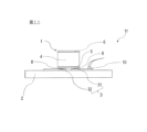


Classifications
-
- H—ELECTRICITY
- H01—ELECTRIC ELEMENTS
- H01G—CAPACITORS; CAPACITORS, RECTIFIERS, DETECTORS, SWITCHING DEVICES, LIGHT-SENSITIVE OR TEMPERATURE-SENSITIVE DEVICES OF THE ELECTROLYTIC TYPE
- H01G13/00—Apparatus specially adapted for manufacturing capacitors; Processes specially adapted for manufacturing capacitors not provided for in groups H01G4/00 - H01G11/00
- H01G13/006—Apparatus or processes for applying terminals
-
- H—ELECTRICITY
- H01—ELECTRIC ELEMENTS
- H01C—RESISTORS
- H01C1/00—Details
- H01C1/01—Mounting; Supporting
- H01C1/014—Mounting; Supporting the resistor being suspended between and being supported by two supporting sections
-
- H—ELECTRICITY
- H01—ELECTRIC ELEMENTS
- H01C—RESISTORS
- H01C1/00—Details
- H01C1/14—Terminals or tapping points specially adapted for resistors; Arrangements of terminals or tapping points on resistors
- H01C1/144—Terminals or tapping points specially adapted for resistors; Arrangements of terminals or tapping points on resistors the terminals or tapping points being welded or soldered
-
- H—ELECTRICITY
- H01—ELECTRIC ELEMENTS
- H01C—RESISTORS
- H01C17/00—Apparatus or processes specially adapted for manufacturing resistors
- H01C17/28—Apparatus or processes specially adapted for manufacturing resistors adapted for applying terminals
- H01C17/281—Apparatus or processes specially adapted for manufacturing resistors adapted for applying terminals by thick film techniques
-
- H—ELECTRICITY
- H01—ELECTRIC ELEMENTS
- H01G—CAPACITORS; CAPACITORS, RECTIFIERS, DETECTORS, SWITCHING DEVICES, LIGHT-SENSITIVE OR TEMPERATURE-SENSITIVE DEVICES OF THE ELECTROLYTIC TYPE
- H01G2/00—Details of capacitors not covered by a single one of groups H01G4/00-H01G11/00
- H01G2/02—Mountings
- H01G2/06—Mountings specially adapted for mounting on a printed-circuit support
-
- H—ELECTRICITY
- H01—ELECTRIC ELEMENTS
- H01G—CAPACITORS; CAPACITORS, RECTIFIERS, DETECTORS, SWITCHING DEVICES, LIGHT-SENSITIVE OR TEMPERATURE-SENSITIVE DEVICES OF THE ELECTROLYTIC TYPE
- H01G2/00—Details of capacitors not covered by a single one of groups H01G4/00-H01G11/00
- H01G2/02—Mountings
- H01G2/06—Mountings specially adapted for mounting on a printed-circuit support
- H01G2/065—Mountings specially adapted for mounting on a printed-circuit support for surface mounting, e.g. chip capacitors
-
- H—ELECTRICITY
- H05—ELECTRIC TECHNIQUES NOT OTHERWISE PROVIDED FOR
- H05K—PRINTED CIRCUITS; CASINGS OR CONSTRUCTIONAL DETAILS OF ELECTRIC APPARATUS; MANUFACTURE OF ASSEMBLAGES OF ELECTRICAL COMPONENTS
- H05K3/00—Apparatus or processes for manufacturing printed circuits
- H05K3/30—Assembling printed circuits with electric components, e.g. with resistors
- H05K3/32—Assembling printed circuits with electric components, e.g. with resistors electrically connecting electric components or wires to printed circuits
- H05K3/328—Assembling printed circuits with electric components, e.g. with resistors electrically connecting electric components or wires to printed circuits by welding
-
- H—ELECTRICITY
- H10—SEMICONDUCTOR DEVICES; ELECTRIC SOLID-STATE DEVICES NOT OTHERWISE PROVIDED FOR
- H10W—GENERIC PACKAGES, INTERCONNECTIONS, CONNECTORS OR OTHER CONSTRUCTIONAL DETAILS OF DEVICES COVERED BY CLASS H10
- H10W72/00—Interconnections or connectors in packages
- H10W72/01—Manufacture or treatment
- H10W72/0198—Manufacture or treatment batch processes
-
- H—ELECTRICITY
- H10—SEMICONDUCTOR DEVICES; ELECTRIC SOLID-STATE DEVICES NOT OTHERWISE PROVIDED FOR
- H10W—GENERIC PACKAGES, INTERCONNECTIONS, CONNECTORS OR OTHER CONSTRUCTIONAL DETAILS OF DEVICES COVERED BY CLASS H10
- H10W72/00—Interconnections or connectors in packages
- H10W72/071—Connecting or disconnecting
- H10W72/072—Connecting or disconnecting of bump connectors
-
- H—ELECTRICITY
- H01—ELECTRIC ELEMENTS
- H01C—RESISTORS
- H01C1/00—Details
- H01C1/01—Mounting; Supporting
-
- H—ELECTRICITY
- H01—ELECTRIC ELEMENTS
- H01C—RESISTORS
- H01C17/00—Apparatus or processes specially adapted for manufacturing resistors
- H01C17/28—Apparatus or processes specially adapted for manufacturing resistors adapted for applying terminals
- H01C17/281—Apparatus or processes specially adapted for manufacturing resistors adapted for applying terminals by thick film techniques
- H01C17/283—Precursor compositions therefor, e.g. pastes, inks, glass frits
-
- H—ELECTRICITY
- H01—ELECTRIC ELEMENTS
- H01G—CAPACITORS; CAPACITORS, RECTIFIERS, DETECTORS, SWITCHING DEVICES, LIGHT-SENSITIVE OR TEMPERATURE-SENSITIVE DEVICES OF THE ELECTROLYTIC TYPE
- H01G4/00—Fixed capacitors; Processes of their manufacture
- H01G4/002—Details
- H01G4/228—Terminals
- H01G4/232—Terminals electrically connecting two or more layers of a stacked or rolled capacitor
-
- H—ELECTRICITY
- H05—ELECTRIC TECHNIQUES NOT OTHERWISE PROVIDED FOR
- H05K—PRINTED CIRCUITS; CASINGS OR CONSTRUCTIONAL DETAILS OF ELECTRIC APPARATUS; MANUFACTURE OF ASSEMBLAGES OF ELECTRICAL COMPONENTS
- H05K1/00—Printed circuits
- H05K1/02—Details
- H05K1/03—Use of materials for the substrate
- H05K1/0306—Inorganic insulating substrates, e.g. ceramic, glass
-
- H—ELECTRICITY
- H05—ELECTRIC TECHNIQUES NOT OTHERWISE PROVIDED FOR
- H05K—PRINTED CIRCUITS; CASINGS OR CONSTRUCTIONAL DETAILS OF ELECTRIC APPARATUS; MANUFACTURE OF ASSEMBLAGES OF ELECTRICAL COMPONENTS
- H05K2201/00—Indexing scheme relating to printed circuits covered by H05K1/00
- H05K2201/03—Conductive materials
- H05K2201/0332—Structure of the conductor
- H05K2201/0364—Conductor shape
- H05K2201/0367—Metallic bump or raised conductor not used as solder bump
-
- H—ELECTRICITY
- H05—ELECTRIC TECHNIQUES NOT OTHERWISE PROVIDED FOR
- H05K—PRINTED CIRCUITS; CASINGS OR CONSTRUCTIONAL DETAILS OF ELECTRIC APPARATUS; MANUFACTURE OF ASSEMBLAGES OF ELECTRICAL COMPONENTS
- H05K2201/00—Indexing scheme relating to printed circuits covered by H05K1/00
- H05K2201/10—Details of components or other objects attached to or integrated in a printed circuit board
- H05K2201/10007—Types of components
- H05K2201/10022—Non-printed resistor
-
- H—ELECTRICITY
- H05—ELECTRIC TECHNIQUES NOT OTHERWISE PROVIDED FOR
- H05K—PRINTED CIRCUITS; CASINGS OR CONSTRUCTIONAL DETAILS OF ELECTRIC APPARATUS; MANUFACTURE OF ASSEMBLAGES OF ELECTRICAL COMPONENTS
- H05K2201/00—Indexing scheme relating to printed circuits covered by H05K1/00
- H05K2201/10—Details of components or other objects attached to or integrated in a printed circuit board
- H05K2201/10007—Types of components
- H05K2201/10196—Variable component, e.g. variable resistor
-
- H—ELECTRICITY
- H10—SEMICONDUCTOR DEVICES; ELECTRIC SOLID-STATE DEVICES NOT OTHERWISE PROVIDED FOR
- H10W—GENERIC PACKAGES, INTERCONNECTIONS, CONNECTORS OR OTHER CONSTRUCTIONAL DETAILS OF DEVICES COVERED BY CLASS H10
- H10W72/00—Interconnections or connectors in packages
- H10W72/071—Connecting or disconnecting
- H10W72/072—Connecting or disconnecting of bump connectors
- H10W72/07231—Techniques
- H10W72/07232—Compression bonding, e.g. thermocompression bonding
-
- H—ELECTRICITY
- H10—SEMICONDUCTOR DEVICES; ELECTRIC SOLID-STATE DEVICES NOT OTHERWISE PROVIDED FOR
- H10W—GENERIC PACKAGES, INTERCONNECTIONS, CONNECTORS OR OTHER CONSTRUCTIONAL DETAILS OF DEVICES COVERED BY CLASS H10
- H10W72/00—Interconnections or connectors in packages
- H10W72/071—Connecting or disconnecting
- H10W72/072—Connecting or disconnecting of bump connectors
- H10W72/07231—Techniques
- H10W72/07235—Applying EM radiation, e.g. induction heating or using a laser
-
- H—ELECTRICITY
- H10—SEMICONDUCTOR DEVICES; ELECTRIC SOLID-STATE DEVICES NOT OTHERWISE PROVIDED FOR
- H10W—GENERIC PACKAGES, INTERCONNECTIONS, CONNECTORS OR OTHER CONSTRUCTIONAL DETAILS OF DEVICES COVERED BY CLASS H10
- H10W90/00—Package configurations
- H10W90/701—Package configurations characterised by the relative positions of pads or connectors relative to package parts
- H10W90/721—Package configurations characterised by the relative positions of pads or connectors relative to package parts of bump connectors
- H10W90/724—Package configurations characterised by the relative positions of pads or connectors relative to package parts of bump connectors between a chip and a stacked insulating package substrate, interposer or RDL
Landscapes
- Engineering & Computer Science (AREA)
- Microelectronics & Electronic Packaging (AREA)
- Power Engineering (AREA)
- Manufacturing & Machinery (AREA)
- Electric Connection Of Electric Components To Printed Circuits (AREA)
- Connections Effected By Soldering, Adhesion, Or Permanent Deformation (AREA)
- Wire Bonding (AREA)
Applications Claiming Priority (3)
| Application Number | Priority Date | Filing Date | Title |
|---|---|---|---|
| DE102021117573.9 | 2021-07-07 | ||
| DE102021117573.9A DE102021117573B4 (de) | 2021-07-07 | 2021-07-07 | Verfahren zur Herstellung einer elektrischen Verbindung zu einem elektronischen Bauteil und einer Chip-Baugruppe |
| PCT/EP2022/067392 WO2023280602A2 (en) | 2021-07-07 | 2022-06-24 | Method for establishing an electric connection to an electronic component and a chip assembly |
Publications (2)
| Publication Number | Publication Date |
|---|---|
| JP2024525426A JP2024525426A (ja) | 2024-07-12 |
| JP7670871B2 true JP7670871B2 (ja) | 2025-04-30 |
Family
ID=82493975
Family Applications (1)
| Application Number | Title | Priority Date | Filing Date |
|---|---|---|---|
| JP2023579614A Active JP7670871B2 (ja) | 2021-07-07 | 2022-06-24 | 電子部品およびチップアセンブリへの電気接続を確立するための方法 |
Country Status (6)
| Country | Link |
|---|---|
| US (1) | US20240282746A1 (de) |
| EP (1) | EP4367691A2 (de) |
| JP (1) | JP7670871B2 (de) |
| CN (1) | CN117616517A (de) |
| DE (1) | DE102021117573B4 (de) |
| WO (1) | WO2023280602A2 (de) |
Families Citing this family (1)
| Publication number | Priority date | Publication date | Assignee | Title |
|---|---|---|---|---|
| DE102024208890A1 (de) * | 2024-09-17 | 2026-03-19 | Robert Bosch Gesellschaft mit beschränkter Haftung | Vorrichtung, insbesondere Sensorvorrichtung mit einer Sensoreinheit, sowie Verfahren zur Herstellung einer solchen Vorrichtung |
Citations (5)
| Publication number | Priority date | Publication date | Assignee | Title |
|---|---|---|---|---|
| JP2000030586A (ja) | 1998-07-15 | 2000-01-28 | Uchihashi Estec Co Ltd | 基板型温度ヒュ−ズの製造方法 |
| JP2009262159A (ja) | 2008-04-22 | 2009-11-12 | Nec Tokin Corp | ダイレクト溶接装置およびその溶接方法 |
| US20100012374A1 (en) | 2008-07-17 | 2010-01-21 | Omron Corporation | Welding method and welding structure of conductive terminals |
| JP2015170575A (ja) | 2014-03-10 | 2015-09-28 | セイコーインスツル株式会社 | 基板ユニット、電気化学セルユニットおよび電気化学セルユニット製造方法 |
| JP2019009361A (ja) | 2017-06-27 | 2019-01-17 | 株式会社村田製作所 | セラミック電子部品及びその実装構造 |
Family Cites Families (16)
| Publication number | Priority date | Publication date | Assignee | Title |
|---|---|---|---|---|
| GB1257148A (de) * | 1970-08-18 | 1971-12-15 | ||
| JPS57187183A (en) * | 1981-05-13 | 1982-11-17 | Toyota Motor Corp | Series spot welding method |
| GB2162686B (en) * | 1984-08-02 | 1988-05-11 | Stc Plc | Thermistors |
| US4717066A (en) * | 1986-02-24 | 1988-01-05 | American Telephone And Telegraph Company, At&T Bell Laboratories | Method of bonding conductors to semiconductor devices |
| JP2666988B2 (ja) * | 1988-11-11 | 1997-10-22 | 株式会社東芝 | リード接続方法 |
| JPH0684687A (ja) * | 1992-08-31 | 1994-03-25 | Toshiba Corp | セラミックチップ部品およびチップ部品実装構造 |
| US5821627A (en) * | 1993-03-11 | 1998-10-13 | Kabushiki Kaisha Toshiba | Electronic circuit device |
| JPH07131275A (ja) * | 1993-10-29 | 1995-05-19 | Kyocera Corp | 水晶発振器の製造方法 |
| JPH0963658A (ja) * | 1995-08-29 | 1997-03-07 | Yamatake Honeywell Co Ltd | リード線の接続構造 |
| US5795818A (en) * | 1996-12-06 | 1998-08-18 | Amkor Technology, Inc. | Integrated circuit chip to substrate interconnection and method |
| JP3509733B2 (ja) * | 2000-10-23 | 2004-03-22 | 日立エーアイシー株式会社 | 電子部品 |
| JP4588630B2 (ja) * | 2005-12-29 | 2010-12-01 | ニチコン株式会社 | チップ状固体電解コンデンサの製造方法 |
| JP2009009994A (ja) * | 2007-06-26 | 2009-01-15 | Shinko Electric Ind Co Ltd | 半導体装置およびその製造方法 |
| DE102008058003B4 (de) | 2008-11-19 | 2012-04-05 | Infineon Technologies Ag | Verfahren zur Herstellung eines Halbleitermoduls und Halbleitermodul |
| JP5647194B2 (ja) | 2012-08-09 | 2014-12-24 | 日本メクトロン株式会社 | フレキシブルプリント基板及びその製造方法 |
| KR102139760B1 (ko) * | 2015-01-22 | 2020-07-31 | 삼성전기주식회사 | 전자 부품 및 그 실장 기판 |
-
2021
- 2021-07-07 DE DE102021117573.9A patent/DE102021117573B4/de active Active
-
2022
- 2022-06-24 US US18/569,905 patent/US20240282746A1/en active Pending
- 2022-06-24 JP JP2023579614A patent/JP7670871B2/ja active Active
- 2022-06-24 WO PCT/EP2022/067392 patent/WO2023280602A2/en not_active Ceased
- 2022-06-24 CN CN202280048060.3A patent/CN117616517A/zh active Pending
- 2022-06-24 EP EP22741159.2A patent/EP4367691A2/de not_active Withdrawn
Patent Citations (6)
| Publication number | Priority date | Publication date | Assignee | Title |
|---|---|---|---|---|
| JP2000030586A (ja) | 1998-07-15 | 2000-01-28 | Uchihashi Estec Co Ltd | 基板型温度ヒュ−ズの製造方法 |
| JP2009262159A (ja) | 2008-04-22 | 2009-11-12 | Nec Tokin Corp | ダイレクト溶接装置およびその溶接方法 |
| US20100012374A1 (en) | 2008-07-17 | 2010-01-21 | Omron Corporation | Welding method and welding structure of conductive terminals |
| JP2010027316A (ja) | 2008-07-17 | 2010-02-04 | Omron Corp | 導電端子の溶接方法および溶接構造 |
| JP2015170575A (ja) | 2014-03-10 | 2015-09-28 | セイコーインスツル株式会社 | 基板ユニット、電気化学セルユニットおよび電気化学セルユニット製造方法 |
| JP2019009361A (ja) | 2017-06-27 | 2019-01-17 | 株式会社村田製作所 | セラミック電子部品及びその実装構造 |
Also Published As
| Publication number | Publication date |
|---|---|
| EP4367691A2 (de) | 2024-05-15 |
| DE102021117573B4 (de) | 2023-04-13 |
| DE102021117573A1 (de) | 2023-01-12 |
| WO2023280602A2 (en) | 2023-01-12 |
| CN117616517A (zh) | 2024-02-27 |
| WO2023280602A3 (en) | 2023-03-23 |
| JP2024525426A (ja) | 2024-07-12 |
| US20240282746A1 (en) | 2024-08-22 |
Similar Documents
| Publication | Publication Date | Title |
|---|---|---|
| US7504312B2 (en) | Stacked electrical resistor pad for optical fiber attachment | |
| JP4085536B2 (ja) | 電気機器およびその製造方法並びに圧接型半導体装置 | |
| CN101483091B (zh) | 包括分流电阻器的装置及其制作方法 | |
| CN100461390C (zh) | 倒装芯片半导体封装件及其制造方法 | |
| CN1165079C (zh) | 内部具有热传输结构的芯片封装 | |
| WO2005091310A1 (ja) | チップ抵抗器およびその製造方法 | |
| JP7670871B2 (ja) | 電子部品およびチップアセンブリへの電気接続を確立するための方法 | |
| CN115732448A (zh) | 高密度和耐用的半导体器件互连 | |
| TWI277106B (en) | Thermistor having improved lead structure and secondary battery having the thermistor | |
| JP6835658B2 (ja) | 試料保持具 | |
| US20210257174A1 (en) | Chip-type fuse with a metal wire type fusible element and manufacturing method for the same | |
| JP6382950B2 (ja) | 電気的に導通した機械的結合部の生成のための固定構造および方法 | |
| US12374648B2 (en) | Connecting strip for discrete and power electronic devices | |
| CN110070969B (zh) | 尤其用于医用植入体的电阻 | |
| US20070084043A1 (en) | Conductive Adhesive Attachment of Capacitor Terminals | |
| EP2840607A1 (de) | Halbleitermodul | |
| JP2013182750A (ja) | 温度ヒューズおよびその製造方法 | |
| JP4403661B2 (ja) | 放熱板を用いた部品の実装構造及びその製造方法 | |
| US20260123507A1 (en) | Method of manufacturing a semiconductor device and corresponding semiconductor device and a semiconductor package | |
| JP2004303956A (ja) | プリント基板の製造方法 | |
| JP6973023B2 (ja) | 半導体装置 | |
| JPH0214536A (ja) | フリップチップ実装構造 | |
| JPH1140716A (ja) | 半導体装置およびその製造方法 | |
| JP4222703B2 (ja) | 半導体装置 | |
| JP6835623B2 (ja) | ヒータ |
Legal Events
| Date | Code | Title | Description |
|---|---|---|---|
| A521 | Request for written amendment filed |
Free format text: JAPANESE INTERMEDIATE CODE: A523 Effective date: 20240222 |
|
| A621 | Written request for application examination |
Free format text: JAPANESE INTERMEDIATE CODE: A621 Effective date: 20240222 |
|
| A977 | Report on retrieval |
Free format text: JAPANESE INTERMEDIATE CODE: A971007 Effective date: 20241121 |
|
| A131 | Notification of reasons for refusal |
Free format text: JAPANESE INTERMEDIATE CODE: A131 Effective date: 20241126 |
|
| A521 | Request for written amendment filed |
Free format text: JAPANESE INTERMEDIATE CODE: A523 Effective date: 20250226 |
|
| TRDD | Decision of grant or rejection written | ||
| A01 | Written decision to grant a patent or to grant a registration (utility model) |
Free format text: JAPANESE INTERMEDIATE CODE: A01 Effective date: 20250408 |
|
| A61 | First payment of annual fees (during grant procedure) |
Free format text: JAPANESE INTERMEDIATE CODE: A61 Effective date: 20250417 |
|
| R150 | Certificate of patent or registration of utility model |
Ref document number: 7670871 Country of ref document: JP Free format text: JAPANESE INTERMEDIATE CODE: R150 |