JP7463577B2 - 表示素子、及び電子機器 - Google Patents
表示素子、及び電子機器 Download PDFInfo
- Publication number
- JP7463577B2 JP7463577B2 JP2023012555A JP2023012555A JP7463577B2 JP 7463577 B2 JP7463577 B2 JP 7463577B2 JP 2023012555 A JP2023012555 A JP 2023012555A JP 2023012555 A JP2023012555 A JP 2023012555A JP 7463577 B2 JP7463577 B2 JP 7463577B2
- Authority
- JP
- Japan
- Prior art keywords
- pixel
- light
- sub
- anode electrode
- reflecting surface
- Prior art date
- Legal status (The legal status is an assumption and is not a legal conclusion. Google has not performed a legal analysis and makes no representation as to the accuracy of the status listed.)
- Active
Links
- 229910010272 inorganic material Inorganic materials 0.000 claims description 6
- 239000011147 inorganic material Substances 0.000 claims description 6
- 238000000034 method Methods 0.000 description 49
- 238000005516 engineering process Methods 0.000 description 42
- 239000010410 layer Substances 0.000 description 36
- 238000010586 diagram Methods 0.000 description 20
- 238000004519 manufacturing process Methods 0.000 description 20
- 229920002120 photoresistant polymer Polymers 0.000 description 18
- 239000012044 organic layer Substances 0.000 description 16
- 239000000463 material Substances 0.000 description 14
- 230000015572 biosynthetic process Effects 0.000 description 10
- 238000000576 coating method Methods 0.000 description 8
- 238000005530 etching Methods 0.000 description 8
- 238000000605 extraction Methods 0.000 description 7
- 230000001681 protective effect Effects 0.000 description 7
- VYPSYNLAJGMNEJ-UHFFFAOYSA-N Silicium dioxide Chemical compound O=[Si]=O VYPSYNLAJGMNEJ-UHFFFAOYSA-N 0.000 description 6
- 230000011514 reflex Effects 0.000 description 6
- 239000000758 substrate Substances 0.000 description 5
- 239000011159 matrix material Substances 0.000 description 4
- 238000005019 vapor deposition process Methods 0.000 description 4
- NCGICGYLBXGBGN-UHFFFAOYSA-N 3-morpholin-4-yl-1-oxa-3-azonia-2-azanidacyclopent-3-en-5-imine;hydrochloride Chemical group Cl.[N-]1OC(=N)C=[N+]1N1CCOCC1 NCGICGYLBXGBGN-UHFFFAOYSA-N 0.000 description 3
- 229910052681 coesite Inorganic materials 0.000 description 3
- 229910052906 cristobalite Inorganic materials 0.000 description 3
- 230000005525 hole transport Effects 0.000 description 3
- 238000012986 modification Methods 0.000 description 3
- 230000004048 modification Effects 0.000 description 3
- 239000011347 resin Substances 0.000 description 3
- 229920005989 resin Polymers 0.000 description 3
- 239000000377 silicon dioxide Substances 0.000 description 3
- 235000012239 silicon dioxide Nutrition 0.000 description 3
- 238000004088 simulation Methods 0.000 description 3
- 229910052682 stishovite Inorganic materials 0.000 description 3
- 229910052905 tridymite Inorganic materials 0.000 description 3
- 229920000178 Acrylic resin Polymers 0.000 description 2
- 239000004925 Acrylic resin Substances 0.000 description 2
- 229910016570 AlCu Inorganic materials 0.000 description 2
- 239000004020 conductor Substances 0.000 description 2
- 230000006866 deterioration Effects 0.000 description 2
- 230000000694 effects Effects 0.000 description 2
- 238000002347 injection Methods 0.000 description 2
- 239000007924 injection Substances 0.000 description 2
- 239000011810 insulating material Substances 0.000 description 2
- 229920001721 polyimide Polymers 0.000 description 2
- 239000009719 polyimide resin Substances 0.000 description 2
- 229920002050 silicone resin Polymers 0.000 description 2
- XUIMIQQOPSSXEZ-UHFFFAOYSA-N Silicon Chemical compound [Si] XUIMIQQOPSSXEZ-UHFFFAOYSA-N 0.000 description 1
- 230000003190 augmentative effect Effects 0.000 description 1
- 238000004364 calculation method Methods 0.000 description 1
- 239000003990 capacitor Substances 0.000 description 1
- 238000005401 electroluminescence Methods 0.000 description 1
- 239000011521 glass Substances 0.000 description 1
- 238000003384 imaging method Methods 0.000 description 1
- 239000000203 mixture Substances 0.000 description 1
- 230000003287 optical effect Effects 0.000 description 1
- 230000000644 propagated effect Effects 0.000 description 1
- 230000001902 propagating effect Effects 0.000 description 1
- 229910052710 silicon Inorganic materials 0.000 description 1
- 239000010703 silicon Substances 0.000 description 1
Images


Classifications
-
- H—ELECTRICITY
- H10—SEMICONDUCTOR DEVICES; ELECTRIC SOLID-STATE DEVICES NOT OTHERWISE PROVIDED FOR
- H10K—ORGANIC ELECTRIC SOLID-STATE DEVICES
- H10K59/00—Integrated devices, or assemblies of multiple devices, comprising at least one organic light-emitting element covered by group H10K50/00
- H10K59/30—Devices specially adapted for multicolour light emission
- H10K59/35—Devices specially adapted for multicolour light emission comprising red-green-blue [RGB] subpixels
- H10K59/352—Devices specially adapted for multicolour light emission comprising red-green-blue [RGB] subpixels the areas of the RGB subpixels being different
-
- H—ELECTRICITY
- H10—SEMICONDUCTOR DEVICES; ELECTRIC SOLID-STATE DEVICES NOT OTHERWISE PROVIDED FOR
- H10K—ORGANIC ELECTRIC SOLID-STATE DEVICES
- H10K50/00—Organic light-emitting devices
- H10K50/80—Constructional details
- H10K50/85—Arrangements for extracting light from the devices
- H10K50/856—Arrangements for extracting light from the devices comprising reflective means
-
- H—ELECTRICITY
- H10—SEMICONDUCTOR DEVICES; ELECTRIC SOLID-STATE DEVICES NOT OTHERWISE PROVIDED FOR
- H10K—ORGANIC ELECTRIC SOLID-STATE DEVICES
- H10K59/00—Integrated devices, or assemblies of multiple devices, comprising at least one organic light-emitting element covered by group H10K50/00
- H10K59/10—OLED displays
- H10K59/12—Active-matrix OLED [AMOLED] displays
- H10K59/121—Active-matrix OLED [AMOLED] displays characterised by the geometry or disposition of pixel elements
- H10K59/1213—Active-matrix OLED [AMOLED] displays characterised by the geometry or disposition of pixel elements the pixel elements being TFTs
-
- H—ELECTRICITY
- H10—SEMICONDUCTOR DEVICES; ELECTRIC SOLID-STATE DEVICES NOT OTHERWISE PROVIDED FOR
- H10K—ORGANIC ELECTRIC SOLID-STATE DEVICES
- H10K59/00—Integrated devices, or assemblies of multiple devices, comprising at least one organic light-emitting element covered by group H10K50/00
- H10K59/10—OLED displays
- H10K59/12—Active-matrix OLED [AMOLED] displays
- H10K59/122—Pixel-defining structures or layers, e.g. banks
-
- H—ELECTRICITY
- H10—SEMICONDUCTOR DEVICES; ELECTRIC SOLID-STATE DEVICES NOT OTHERWISE PROVIDED FOR
- H10K—ORGANIC ELECTRIC SOLID-STATE DEVICES
- H10K59/00—Integrated devices, or assemblies of multiple devices, comprising at least one organic light-emitting element covered by group H10K50/00
- H10K59/30—Devices specially adapted for multicolour light emission
- H10K59/35—Devices specially adapted for multicolour light emission comprising red-green-blue [RGB] subpixels
- H10K59/351—Devices specially adapted for multicolour light emission comprising red-green-blue [RGB] subpixels comprising more than three subpixels, e.g. red-green-blue-white [RGBW]
-
- H—ELECTRICITY
- H10—SEMICONDUCTOR DEVICES; ELECTRIC SOLID-STATE DEVICES NOT OTHERWISE PROVIDED FOR
- H10K—ORGANIC ELECTRIC SOLID-STATE DEVICES
- H10K59/00—Integrated devices, or assemblies of multiple devices, comprising at least one organic light-emitting element covered by group H10K50/00
- H10K59/30—Devices specially adapted for multicolour light emission
- H10K59/35—Devices specially adapted for multicolour light emission comprising red-green-blue [RGB] subpixels
- H10K59/353—Devices specially adapted for multicolour light emission comprising red-green-blue [RGB] subpixels characterised by the geometrical arrangement of the RGB subpixels
-
- H—ELECTRICITY
- H10—SEMICONDUCTOR DEVICES; ELECTRIC SOLID-STATE DEVICES NOT OTHERWISE PROVIDED FOR
- H10K—ORGANIC ELECTRIC SOLID-STATE DEVICES
- H10K59/00—Integrated devices, or assemblies of multiple devices, comprising at least one organic light-emitting element covered by group H10K50/00
- H10K59/30—Devices specially adapted for multicolour light emission
- H10K59/38—Devices specially adapted for multicolour light emission comprising colour filters or colour changing media [CCM]
-
- H—ELECTRICITY
- H10—SEMICONDUCTOR DEVICES; ELECTRIC SOLID-STATE DEVICES NOT OTHERWISE PROVIDED FOR
- H10K—ORGANIC ELECTRIC SOLID-STATE DEVICES
- H10K59/00—Integrated devices, or assemblies of multiple devices, comprising at least one organic light-emitting element covered by group H10K50/00
- H10K59/80—Constructional details
- H10K59/875—Arrangements for extracting light from the devices
- H10K59/878—Arrangements for extracting light from the devices comprising reflective means
-
- G—PHYSICS
- G09—EDUCATION; CRYPTOGRAPHY; DISPLAY; ADVERTISING; SEALS
- G09G—ARRANGEMENTS OR CIRCUITS FOR CONTROL OF INDICATING DEVICES USING STATIC MEANS TO PRESENT VARIABLE INFORMATION
- G09G2300/00—Aspects of the constitution of display devices
- G09G2300/04—Structural and physical details of display devices
- G09G2300/0439—Pixel structures
- G09G2300/0452—Details of colour pixel setup, e.g. pixel composed of a red, a blue and two green components
-
- G—PHYSICS
- G09—EDUCATION; CRYPTOGRAPHY; DISPLAY; ADVERTISING; SEALS
- G09G—ARRANGEMENTS OR CIRCUITS FOR CONTROL OF INDICATING DEVICES USING STATIC MEANS TO PRESENT VARIABLE INFORMATION
- G09G2320/00—Control of display operating conditions
- G09G2320/02—Improving the quality of display appearance
- G09G2320/0233—Improving the luminance or brightness uniformity across the screen
-
- G—PHYSICS
- G09—EDUCATION; CRYPTOGRAPHY; DISPLAY; ADVERTISING; SEALS
- G09G—ARRANGEMENTS OR CIRCUITS FOR CONTROL OF INDICATING DEVICES USING STATIC MEANS TO PRESENT VARIABLE INFORMATION
- G09G2320/00—Control of display operating conditions
- G09G2320/04—Maintaining the quality of display appearance
- G09G2320/043—Preventing or counteracting the effects of ageing
-
- G—PHYSICS
- G09—EDUCATION; CRYPTOGRAPHY; DISPLAY; ADVERTISING; SEALS
- G09G—ARRANGEMENTS OR CIRCUITS FOR CONTROL OF INDICATING DEVICES USING STATIC MEANS TO PRESENT VARIABLE INFORMATION
- G09G3/00—Control arrangements or circuits, of interest only in connection with visual indicators other than cathode-ray tubes
- G09G3/20—Control arrangements or circuits, of interest only in connection with visual indicators other than cathode-ray tubes for presentation of an assembly of a number of characters, e.g. a page, by composing the assembly by combination of individual elements arranged in a matrix no fixed position being assigned to or needed to be assigned to the individual characters or partial characters
- G09G3/22—Control arrangements or circuits, of interest only in connection with visual indicators other than cathode-ray tubes for presentation of an assembly of a number of characters, e.g. a page, by composing the assembly by combination of individual elements arranged in a matrix no fixed position being assigned to or needed to be assigned to the individual characters or partial characters using controlled light sources
- G09G3/30—Control arrangements or circuits, of interest only in connection with visual indicators other than cathode-ray tubes for presentation of an assembly of a number of characters, e.g. a page, by composing the assembly by combination of individual elements arranged in a matrix no fixed position being assigned to or needed to be assigned to the individual characters or partial characters using controlled light sources using electroluminescent panels
- G09G3/32—Control arrangements or circuits, of interest only in connection with visual indicators other than cathode-ray tubes for presentation of an assembly of a number of characters, e.g. a page, by composing the assembly by combination of individual elements arranged in a matrix no fixed position being assigned to or needed to be assigned to the individual characters or partial characters using controlled light sources using electroluminescent panels semiconductive, e.g. using light-emitting diodes [LED]
- G09G3/3208—Control arrangements or circuits, of interest only in connection with visual indicators other than cathode-ray tubes for presentation of an assembly of a number of characters, e.g. a page, by composing the assembly by combination of individual elements arranged in a matrix no fixed position being assigned to or needed to be assigned to the individual characters or partial characters using controlled light sources using electroluminescent panels semiconductive, e.g. using light-emitting diodes [LED] organic, e.g. using organic light-emitting diodes [OLED]
- G09G3/3225—Control arrangements or circuits, of interest only in connection with visual indicators other than cathode-ray tubes for presentation of an assembly of a number of characters, e.g. a page, by composing the assembly by combination of individual elements arranged in a matrix no fixed position being assigned to or needed to be assigned to the individual characters or partial characters using controlled light sources using electroluminescent panels semiconductive, e.g. using light-emitting diodes [LED] organic, e.g. using organic light-emitting diodes [OLED] using an active matrix
-
- G—PHYSICS
- G09—EDUCATION; CRYPTOGRAPHY; DISPLAY; ADVERTISING; SEALS
- G09G—ARRANGEMENTS OR CIRCUITS FOR CONTROL OF INDICATING DEVICES USING STATIC MEANS TO PRESENT VARIABLE INFORMATION
- G09G3/00—Control arrangements or circuits, of interest only in connection with visual indicators other than cathode-ray tubes
- G09G3/20—Control arrangements or circuits, of interest only in connection with visual indicators other than cathode-ray tubes for presentation of an assembly of a number of characters, e.g. a page, by composing the assembly by combination of individual elements arranged in a matrix no fixed position being assigned to or needed to be assigned to the individual characters or partial characters
- G09G3/22—Control arrangements or circuits, of interest only in connection with visual indicators other than cathode-ray tubes for presentation of an assembly of a number of characters, e.g. a page, by composing the assembly by combination of individual elements arranged in a matrix no fixed position being assigned to or needed to be assigned to the individual characters or partial characters using controlled light sources
- G09G3/30—Control arrangements or circuits, of interest only in connection with visual indicators other than cathode-ray tubes for presentation of an assembly of a number of characters, e.g. a page, by composing the assembly by combination of individual elements arranged in a matrix no fixed position being assigned to or needed to be assigned to the individual characters or partial characters using controlled light sources using electroluminescent panels
- G09G3/32—Control arrangements or circuits, of interest only in connection with visual indicators other than cathode-ray tubes for presentation of an assembly of a number of characters, e.g. a page, by composing the assembly by combination of individual elements arranged in a matrix no fixed position being assigned to or needed to be assigned to the individual characters or partial characters using controlled light sources using electroluminescent panels semiconductive, e.g. using light-emitting diodes [LED]
- G09G3/3208—Control arrangements or circuits, of interest only in connection with visual indicators other than cathode-ray tubes for presentation of an assembly of a number of characters, e.g. a page, by composing the assembly by combination of individual elements arranged in a matrix no fixed position being assigned to or needed to be assigned to the individual characters or partial characters using controlled light sources using electroluminescent panels semiconductive, e.g. using light-emitting diodes [LED] organic, e.g. using organic light-emitting diodes [OLED]
- G09G3/3266—Details of drivers for scan electrodes
-
- G—PHYSICS
- G09—EDUCATION; CRYPTOGRAPHY; DISPLAY; ADVERTISING; SEALS
- G09G—ARRANGEMENTS OR CIRCUITS FOR CONTROL OF INDICATING DEVICES USING STATIC MEANS TO PRESENT VARIABLE INFORMATION
- G09G3/00—Control arrangements or circuits, of interest only in connection with visual indicators other than cathode-ray tubes
- G09G3/20—Control arrangements or circuits, of interest only in connection with visual indicators other than cathode-ray tubes for presentation of an assembly of a number of characters, e.g. a page, by composing the assembly by combination of individual elements arranged in a matrix no fixed position being assigned to or needed to be assigned to the individual characters or partial characters
- G09G3/22—Control arrangements or circuits, of interest only in connection with visual indicators other than cathode-ray tubes for presentation of an assembly of a number of characters, e.g. a page, by composing the assembly by combination of individual elements arranged in a matrix no fixed position being assigned to or needed to be assigned to the individual characters or partial characters using controlled light sources
- G09G3/30—Control arrangements or circuits, of interest only in connection with visual indicators other than cathode-ray tubes for presentation of an assembly of a number of characters, e.g. a page, by composing the assembly by combination of individual elements arranged in a matrix no fixed position being assigned to or needed to be assigned to the individual characters or partial characters using controlled light sources using electroluminescent panels
- G09G3/32—Control arrangements or circuits, of interest only in connection with visual indicators other than cathode-ray tubes for presentation of an assembly of a number of characters, e.g. a page, by composing the assembly by combination of individual elements arranged in a matrix no fixed position being assigned to or needed to be assigned to the individual characters or partial characters using controlled light sources using electroluminescent panels semiconductive, e.g. using light-emitting diodes [LED]
- G09G3/3208—Control arrangements or circuits, of interest only in connection with visual indicators other than cathode-ray tubes for presentation of an assembly of a number of characters, e.g. a page, by composing the assembly by combination of individual elements arranged in a matrix no fixed position being assigned to or needed to be assigned to the individual characters or partial characters using controlled light sources using electroluminescent panels semiconductive, e.g. using light-emitting diodes [LED] organic, e.g. using organic light-emitting diodes [OLED]
- G09G3/3275—Details of drivers for data electrodes
-
- H—ELECTRICITY
- H10—SEMICONDUCTOR DEVICES; ELECTRIC SOLID-STATE DEVICES NOT OTHERWISE PROVIDED FOR
- H10K—ORGANIC ELECTRIC SOLID-STATE DEVICES
- H10K2102/00—Constructional details relating to the organic devices covered by this subclass
- H10K2102/301—Details of OLEDs
- H10K2102/302—Details of OLEDs of OLED structures
- H10K2102/3023—Direction of light emission
Landscapes
- Engineering & Computer Science (AREA)
- Microelectronics & Electronic Packaging (AREA)
- Physics & Mathematics (AREA)
- Optics & Photonics (AREA)
- Geometry (AREA)
- Electroluminescent Light Sources (AREA)
- Devices For Indicating Variable Information By Combining Individual Elements (AREA)
Description
2.変形例
3.電子機器の例
図1は、本技術を適用した表示素子の一実施の形態の構成の例を示すブロック図である。
ところで、有機EL表示素子において、画素を構成する各サブ画素の輝度を向上させるためには、サブ画素のサイズを変えることで、対応することが可能となる。しかしながら、画素のうちの特定のサブ画素のサイズを大きくして、発光面積を増大させる方法をとった場合には、画素ピッチが変わってしまうため、高精細化が困難となる。
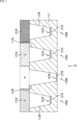
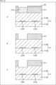
図5は、第1の実施の形態の画素の構造の一部を示す要部断面図である。以下、この要部断面図を参照しながら、第1の実施の形態の画素10の構造を説明する。
図6は、第2の実施の形態の画素の構造の一部を示す要部断面図である。以下、この要部断面図を参照しながら、第2の実施の形態の画素10の構造を説明する。
図7は、第3の実施の形態の画素の構造の一部を示す要部断面図である。以下、この要部断面図を参照しながら、第3の実施の形態の画素10の構造を説明する。
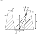
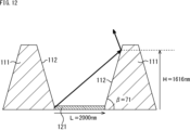
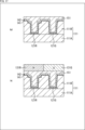
次に、図8乃至図12を参照して、リフレクタ112の構造の詳細について説明する。
tan-1 (H / (L + t)) = θ + β - 90
tan(θ + β - 90) = H / (L + t) ・・・(5)
= 1000 × tan(51.3°+ 71°- 90°) / (1 - (tan(51.3°+ 71°- 90°) / tan71°))
= 808.07
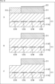
次に、図13乃至図17を参照して、本技術の実施の形態の画素の製造工程の第1の例の流れを説明する。
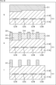
次に、図18乃至図22を参照して、本技術の実施の形態の画素の製造工程の第2の例の流れを説明する。
図23は、本技術を適用した表示素子が適用される電子機器(撮像装置)として、一眼レフカメラ(レンズ交換式一眼レフレックスタイプのデジタルカメラ)の外観の例を示している。
図24は、本技術を適用した表示素子が適用される電子機器として、ヘッドマウントディスプレイ(HMD:Head Mounted Display)の外観の例を示している。
なお、上述した図23及び図24においては、本技術を適用した表示素子が適用される電子機器として、一眼レフカメラとヘッドマウントディスプレイを例示したが、例えば、スマートフォン、テレビ受像機、パーソナルコンピュータ、ビデオカメラ、携帯電話機、ゲーム機、ウェアラブル機器などの電子機器に、本技術を適用した表示素子が適用されるようにしてもよい。
複数のサブ画素からなる画素を2次元状に配置した表示領域を有し、
前記画素は、前記サブ画素ごとに、発光部に対する光反射部の高さを調整している
表示素子。
(2)
前記サブ画素ごとに、前記光反射部の積層方向の斜面の高さを調整している
前記(1)に記載の表示素子。
(3)
前記サブ画素ごとに、前記光反射部の斜面の高さが異なる
前記(2)に記載の表示素子。
(4)
複数の前記サブ画素のうち、特定のサブ画素のみ、前記光反射部の斜面の高さが異なる
前記(2)に記載の表示素子。
(5)
前記サブ画素ごとに、前記発光部の積層方向の位置を調整している
前記(1)に記載の表示素子。
(6)
前記サブ画素ごとに、前記発光部の位置が異なる
前記(5)に記載の表示素子。
(7)
複数の前記サブ画素のうち、特定のサブ画素のみ、前記発光部の位置が異なる
前記(5)に記載の表示素子。
(8)
前記光反射部の斜面の高さは、前記光反射部の斜面の角度と、前記発光部の発光部分の幅に応じて調整される
前記(1)乃至(7)のいずれかに記載の表示素子。
(9)
前記画素は、3つの基本色光を発する第1のサブ画素、第2のサブ画素、及び第3のサブ画素と、非基本色光を発する第4のサブ画素からなる
前記(1)乃至(8)のいずれかに記載の表示素子。
(10)
前記基本色光は、赤色光、緑色光、及び青色光であり、
前記非基本色光は、白色光である
前記(9)に記載の表示素子。
(11)
前記サブ画素は、前記発光部として自発光する発光素子を有する画素であり、
前記発光素子は、電極と、発光層を有する有機層から構成される
前記(1)乃至(10)のいずれかに記載の表示素子。
(12)
複数のサブ画素からなる画素を2次元状に配置した表示領域を有し、
前記画素は、前記サブ画素ごとに、発光部に対する光反射部の高さを調整している
表示素子を備える電子機器。
Claims (4)
- 第1の光を発する第1のサブ画素と、前記第1の光と異なる第2の光を発する第2のサブ画素を含む画素を2次元状に配置した表示領域を有し、
前記第1のサブ画素は、第1のアノード電極を含む第1の有機発光素子を有し、
前記第2のサブ画素は、第2のアノード電極を含む第2の有機発光素子を有し、
前記画素は、
無機材料からなる第1の部材を有し、
前記第1の部材は、前記第1の有機発光素子からの光を反射する第1の反射面と、前記第2の有機発光素子からの光を反射する第2の反射面を形成しており、
前記第1のアノード電極の下面から、前記第1の反射面を形成した前記第1の部材の上面までの積層方向の距離である第1の距離と、前記第2のアノード電極の下面から、前記第2の反射面を形成した前記第1の部材の上面までの積層方向の距離である第2の距離とが異なり、
前記第1の部材は、
前記第1のアノード電極が露出した第1の開口部に対する側壁が、所定の傾斜角で傾斜して前記第1の反射面を形成し、
前記第2のアノード電極が露出した第2の開口部に対する側壁が、所定の傾斜角で傾斜して前記第2の反射面を形成し、
前記第1のアノード電極の少なくとも一部の領域は、前記第1の反射面を形成する側壁と接し、
前記第2のアノード電極の少なくとも一部の領域は、前記第2の反射面を形成する側壁と接し、
前記画素における前記第1のサブ画素と前記第2のサブ画素は、発光面積と画素ピッチが同じである
表示素子。 - 第1の屈折率を有する前記第1の部材と、
前記第1の屈折率と異なる第2の屈折率を有する第2の部材であって、前記第1の開口部から露出した前記第1のアノード電極及び前記第1の反射面による第1の凹部と、前記第2の開口部から露出した前記第2のアノード電極及び前記第2の反射面による第2の凹部に埋め込まれた前記第2の部材と
により光反射層が形成される
請求項1に記載の表示素子。 - 前記画素は、
第3のアノード電極を含む第3の有機発光素子を有し、前記第1の光、及び前記第2の光と異なる第3の光を発する第3のサブ画素と、
第4のアノード電極を含む第4の有機発光素子を有し、前記第1の光、前記第2の光、及び前記第3の光と異なる第4の光を発する第4のサブ画素と
をさらに含み、
前記画素における前記第1のサブ画素と、前記第2のサブ画素と、前記第3のサブ画素と、前記第4のサブ画素は、発光面積と画素ピッチが同じであり、
前記第1の部材は、前記第3の有機発光素子からの光を反射する第3の反射面と、前記第4の有機発光素子からの光を反射する第4の反射面をさらに形成しており、
前記第3のアノード電極の下面から、前記第3の反射面を形成した前記第1の部材の上面までの積層方向の距離である第3の距離と、前記第4のアノード電極の下面から、前記第4の反射面を形成した前記第1の部材の上面までの積層方向の距離である第4の距離は、前記第1の距離及び前記第2の距離の少なくとも一方と異なり、
前記第1の部材は、
前記第3のアノード電極が露出した第3の開口部に対する側壁が、所定の傾斜角で傾斜して前記第3の反射面を形成し、
前記第4のアノード電極が露出した第4の開口部に対する側壁が、所定の傾斜角で傾斜して前記第4の反射面を形成し、
前記第3のアノード電極の少なくとも一部の領域は、前記第3の反射面を形成する側壁と接し、
前記第4のアノード電極の少なくとも一部の領域は、前記第4の反射面を形成する側壁と接する
請求項1に記載の表示素子。 - 第1の光を発する第1のサブ画素と、前記第1の光と異なる第2の光を発する第2のサブ画素を含む画素を2次元状に配置した表示領域を有し、
前記第1のサブ画素は、第1のアノード電極を含む第1の有機発光素子を有し、
前記第2のサブ画素は、第2のアノード電極を含む第2の有機発光素子を有し、
前記画素は、
無機材料からなる第1の部材を有し、
前記第1の部材は、前記第1の有機発光素子からの光を反射する第1の反射面と、前記第2の有機発光素子からの光を反射する第2の反射面を形成しており、
前記第1のアノード電極の下面から、前記第1の反射面を形成した前記第1の部材の上面までの積層方向の距離である第1の距離と、前記第2のアノード電極の下面から、前記第2の反射面を形成した前記第1の部材の上面までの積層方向の距離である第2の距離とが異なり、
前記第1の部材は、
前記第1のアノード電極が露出した第1の開口部に対する側壁が、所定の傾斜角で傾斜して前記第1の反射面を形成し、
前記第2のアノード電極が露出した第2の開口部に対する側壁が、所定の傾斜角で傾斜して前記第2の反射面を形成し、
前記第1のアノード電極の少なくとも一部の領域は、前記第1の反射面を形成する側壁と接し、
前記第2のアノード電極の少なくとも一部の領域は、前記第2の反射面を形成する側壁と接し、
前記画素における前記第1のサブ画素と前記第2のサブ画素は、発光面積と画素ピッチが同じである
表示素子を備える電子機器。
Priority Applications (1)
| Application Number | Priority Date | Filing Date | Title |
|---|---|---|---|
| JP2023012555A JP7463577B2 (ja) | 2017-12-26 | 2023-01-31 | 表示素子、及び電子機器 |
Applications Claiming Priority (2)
| Application Number | Priority Date | Filing Date | Title |
|---|---|---|---|
| JP2017248697A JP2019114484A (ja) | 2017-12-26 | 2017-12-26 | 表示素子、及び電子機器 |
| JP2023012555A JP7463577B2 (ja) | 2017-12-26 | 2023-01-31 | 表示素子、及び電子機器 |
Related Parent Applications (1)
| Application Number | Title | Priority Date | Filing Date |
|---|---|---|---|
| JP2017248697A Division JP2019114484A (ja) | 2017-12-26 | 2017-12-26 | 表示素子、及び電子機器 |
Publications (2)
| Publication Number | Publication Date |
|---|---|
| JP2023055824A JP2023055824A (ja) | 2023-04-18 |
| JP7463577B2 true JP7463577B2 (ja) | 2024-04-08 |
Family
ID=65023970
Family Applications (2)
| Application Number | Title | Priority Date | Filing Date |
|---|---|---|---|
| JP2017248697A Pending JP2019114484A (ja) | 2017-12-26 | 2017-12-26 | 表示素子、及び電子機器 |
| JP2023012555A Active JP7463577B2 (ja) | 2017-12-26 | 2023-01-31 | 表示素子、及び電子機器 |
Family Applications Before (1)
| Application Number | Title | Priority Date | Filing Date |
|---|---|---|---|
| JP2017248697A Pending JP2019114484A (ja) | 2017-12-26 | 2017-12-26 | 表示素子、及び電子機器 |
Country Status (6)
| Country | Link |
|---|---|
| US (2) | US11569483B2 (ja) |
| EP (1) | EP3732739A1 (ja) |
| JP (2) | JP2019114484A (ja) |
| KR (2) | KR20250035026A (ja) |
| CN (3) | CN111512460B (ja) |
| WO (1) | WO2019131487A1 (ja) |
Families Citing this family (4)
| Publication number | Priority date | Publication date | Assignee | Title |
|---|---|---|---|---|
| KR102890077B1 (ko) * | 2019-08-02 | 2025-11-24 | 삼성디스플레이 주식회사 | 표시 장치 및 표시 장치의 제조 방법 |
| CN112133734B (zh) * | 2020-09-29 | 2022-08-30 | 湖北长江新型显示产业创新中心有限公司 | 显示面板及显示装置 |
| TWI771896B (zh) | 2021-02-04 | 2022-07-21 | 錼創顯示科技股份有限公司 | 微型發光二極體顯示面板 |
| CN112786766B (zh) * | 2021-02-04 | 2023-05-16 | 錼创显示科技股份有限公司 | 微型发光二极管显示面板 |
Citations (12)
| Publication number | Priority date | Publication date | Assignee | Title |
|---|---|---|---|---|
| JP2006278257A (ja) | 2005-03-30 | 2006-10-12 | Sony Corp | 有機発光装置およびその製造方法 |
| JP2007503093A (ja) | 2003-08-19 | 2007-02-15 | イーストマン コダック カンパニー | マイクロキャビティ・ガモット・サブ画素を有するoledデバイス |
| JP2007248484A (ja) | 2006-03-13 | 2007-09-27 | Sony Corp | 表示装置 |
| JP2009049135A (ja) | 2007-08-17 | 2009-03-05 | Sony Corp | 表示装置 |
| JP2009206041A (ja) | 2008-02-29 | 2009-09-10 | Sony Corp | 有機発光装置およびその製造方法 |
| JP2010056017A (ja) | 2008-08-29 | 2010-03-11 | Fujifilm Corp | カラー表示装置及びその製造方法 |
| US20120176025A1 (en) | 2011-01-10 | 2012-07-12 | Samsung Mobile Display Co., Ltd. | Organic Light Emitting Display Apparatus and Method of Manufacturing the Same |
| JP2013191533A (ja) | 2012-02-17 | 2013-09-26 | Sony Corp | 表示装置及び表示装置の製造方法 |
| WO2014148263A1 (ja) | 2013-03-21 | 2014-09-25 | ソニー株式会社 | 表示装置およびその製造方法ならびに電子機器 |
| US20140332762A1 (en) | 2013-05-13 | 2014-11-13 | Samsung Display Co., Ltd. | Organic electroluminescent display |
| WO2016158074A1 (ja) | 2015-04-01 | 2016-10-06 | ソニー株式会社 | 表示装置、表示装置の製造方法、及び、電子機器 |
| WO2017051622A1 (ja) | 2015-09-25 | 2017-03-30 | ソニー株式会社 | 表示装置及びその製造方法 |
Family Cites Families (24)
| Publication number | Priority date | Publication date | Assignee | Title |
|---|---|---|---|---|
| JP4693253B2 (ja) * | 2001-01-30 | 2011-06-01 | 株式会社半導体エネルギー研究所 | 発光装置、電子機器 |
| US7129634B2 (en) * | 2004-04-07 | 2006-10-31 | Eastman Kodak Company | Color OLED with added color gamut pixels |
| JP4192837B2 (ja) * | 2004-04-30 | 2008-12-10 | セイコーエプソン株式会社 | 表示素子及び表示素子の製造方法 |
| KR20100066416A (ko) * | 2007-09-06 | 2010-06-17 | 소니 가부시끼가이샤 | 광 추출 소자, 광 추출 소자의 제조 방법 및 표시 장치 |
| JP2009110873A (ja) * | 2007-10-31 | 2009-05-21 | Toppan Printing Co Ltd | 表示装置 |
| JP5258412B2 (ja) * | 2008-06-24 | 2013-08-07 | キヤノン株式会社 | 発光素子、発光素子を用いた表示装置及び発光素子の製造方法 |
| WO2010143360A1 (ja) * | 2009-06-11 | 2010-12-16 | パナソニック株式会社 | 有機elディスプレイ |
| JP2014225323A (ja) * | 2011-09-12 | 2014-12-04 | シャープ株式会社 | 発光デバイス、表示装置、及び照明装置 |
| JP5927476B2 (ja) * | 2011-10-03 | 2016-06-01 | 株式会社Joled | 表示装置および電子機器 |
| US9281451B2 (en) * | 2012-02-17 | 2016-03-08 | Industrial Technology Research Institute | Light emitting element and fabricating method thereof |
| KR101990116B1 (ko) * | 2012-10-22 | 2019-10-01 | 삼성디스플레이 주식회사 | 유기발광장치 및 그것의 제조방법 |
| TWI674671B (zh) * | 2013-05-28 | 2019-10-11 | 日商新力股份有限公司 | 顯示裝置及電子機器 |
| JP6191287B2 (ja) * | 2013-07-05 | 2017-09-06 | ソニー株式会社 | 表示装置 |
| JP2016081562A (ja) * | 2014-10-09 | 2016-05-16 | ソニー株式会社 | 表示装置、表示装置の製造方法および電子機器 |
| JP5918340B2 (ja) * | 2014-11-25 | 2016-05-18 | ユー・ディー・シー アイルランド リミテッド | カラー表示装置及びその製造方法 |
| CN105070739B (zh) * | 2015-08-17 | 2018-06-01 | 京东方科技集团股份有限公司 | 显示背板及其制作方法、显示装置 |
| JP2017067999A (ja) * | 2015-09-30 | 2017-04-06 | セイコーエプソン株式会社 | 電気光学装置用基板、電気光学装置、電子機器 |
| JP6727848B2 (ja) * | 2016-02-26 | 2020-07-22 | 株式会社ジャパンディスプレイ | 表示装置 |
| EP3240036B1 (en) * | 2016-04-29 | 2024-05-01 | LG Display Co., Ltd. | Organic light-emitting display device and method of manufacturing the same |
| KR102525501B1 (ko) * | 2016-05-23 | 2023-04-24 | 엘지디스플레이 주식회사 | 유기 발광 표시 장치 |
| JP7229777B2 (ja) * | 2016-06-03 | 2023-02-28 | コーニング インコーポレイテッド | Oledディスプレイ用光取り出し装置および方法ならびに、それらを使用するoledディスプレイ |
| JP6715708B2 (ja) * | 2016-07-08 | 2020-07-01 | 株式会社ジャパンディスプレイ | 表示装置 |
| US10141377B2 (en) * | 2016-07-29 | 2018-11-27 | Lg Display Co., Ltd. | Electroluminescent display device |
| CN108400154B (zh) * | 2018-04-11 | 2019-12-24 | 武汉华星光电半导体显示技术有限公司 | Oled面板 |
-
2017
- 2017-12-26 JP JP2017248697A patent/JP2019114484A/ja active Pending
-
2018
- 2018-12-21 CN CN201880082731.1A patent/CN111512460B/zh active Active
- 2018-12-21 US US16/955,917 patent/US11569483B2/en active Active
- 2018-12-21 CN CN202410983917.1A patent/CN118922014A/zh active Pending
- 2018-12-21 KR KR1020257006365A patent/KR20250035026A/ko active Pending
- 2018-12-21 KR KR1020207017496A patent/KR102775402B1/ko active Active
- 2018-12-21 WO PCT/JP2018/047187 patent/WO2019131487A1/en not_active Ceased
- 2018-12-21 CN CN202410983931.1A patent/CN118922015A/zh active Pending
- 2018-12-21 EP EP18834078.0A patent/EP3732739A1/en active Pending
-
2023
- 2023-01-31 JP JP2023012555A patent/JP7463577B2/ja active Active
- 2023-02-01 US US17/987,269 patent/US20230292543A1/en active Pending
Patent Citations (12)
| Publication number | Priority date | Publication date | Assignee | Title |
|---|---|---|---|---|
| JP2007503093A (ja) | 2003-08-19 | 2007-02-15 | イーストマン コダック カンパニー | マイクロキャビティ・ガモット・サブ画素を有するoledデバイス |
| JP2006278257A (ja) | 2005-03-30 | 2006-10-12 | Sony Corp | 有機発光装置およびその製造方法 |
| JP2007248484A (ja) | 2006-03-13 | 2007-09-27 | Sony Corp | 表示装置 |
| JP2009049135A (ja) | 2007-08-17 | 2009-03-05 | Sony Corp | 表示装置 |
| JP2009206041A (ja) | 2008-02-29 | 2009-09-10 | Sony Corp | 有機発光装置およびその製造方法 |
| JP2010056017A (ja) | 2008-08-29 | 2010-03-11 | Fujifilm Corp | カラー表示装置及びその製造方法 |
| US20120176025A1 (en) | 2011-01-10 | 2012-07-12 | Samsung Mobile Display Co., Ltd. | Organic Light Emitting Display Apparatus and Method of Manufacturing the Same |
| JP2013191533A (ja) | 2012-02-17 | 2013-09-26 | Sony Corp | 表示装置及び表示装置の製造方法 |
| WO2014148263A1 (ja) | 2013-03-21 | 2014-09-25 | ソニー株式会社 | 表示装置およびその製造方法ならびに電子機器 |
| US20140332762A1 (en) | 2013-05-13 | 2014-11-13 | Samsung Display Co., Ltd. | Organic electroluminescent display |
| WO2016158074A1 (ja) | 2015-04-01 | 2016-10-06 | ソニー株式会社 | 表示装置、表示装置の製造方法、及び、電子機器 |
| WO2017051622A1 (ja) | 2015-09-25 | 2017-03-30 | ソニー株式会社 | 表示装置及びその製造方法 |
Also Published As
| Publication number | Publication date |
|---|---|
| KR20250035026A (ko) | 2025-03-11 |
| KR102775402B1 (ko) | 2025-03-05 |
| EP3732739A1 (en) | 2020-11-04 |
| CN118922015A (zh) | 2024-11-08 |
| CN118922014A (zh) | 2024-11-08 |
| WO2019131487A1 (en) | 2019-07-04 |
| KR20200094755A (ko) | 2020-08-07 |
| CN111512460B (zh) | 2024-08-06 |
| US20210074954A1 (en) | 2021-03-11 |
| US20230292543A1 (en) | 2023-09-14 |
| JP2023055824A (ja) | 2023-04-18 |
| US11569483B2 (en) | 2023-01-31 |
| JP2019114484A (ja) | 2019-07-11 |
| CN111512460A (zh) | 2020-08-07 |
Similar Documents
| Publication | Publication Date | Title |
|---|---|---|
| JP7463577B2 (ja) | 表示素子、及び電子機器 | |
| CN111916480B (zh) | 显示装置和电子设备 | |
| CN108922916B (zh) | 发光装置以及电子设备 | |
| US12349536B2 (en) | Electro-optical device and electronic apparatus | |
| JP7047811B2 (ja) | 表示装置、および電子機器 | |
| JP2023052370A (ja) | 表示装置及び電子機器 | |
| JP2017073268A (ja) | 有機el装置、有機el装置の製造方法、電子機器 | |
| JP6696193B2 (ja) | 電気光学装置、および電子機器 | |
| CN111261791B (zh) | 显示装置 | |
| JP7711781B2 (ja) | 表示装置、および電子機器 | |
| US11342538B2 (en) | Organic EL display device having reflection transmission portion, and electronic apparatus | |
| WO2020145148A1 (ja) | 表示装置 | |
| JP2018088381A (ja) | 有機el装置および有機el装置の製造方法 | |
| JP6318693B2 (ja) | 表示装置及び電子機器 | |
| CN112289943B (zh) | 发光装置和电子设备 | |
| CN111244138A (zh) | 电致发光显示装置 | |
| WO2022124401A1 (ja) | 表示装置および電子機器 | |
| CN112289944B (zh) | 发光装置和电子设备 | |
| US20250089540A1 (en) | Display device, method for manufacturing the same, and electronic apparatus | |
| JP2024126259A (ja) | 表示装置および電子機器 |
Legal Events
| Date | Code | Title | Description |
|---|---|---|---|
| A521 | Request for written amendment filed |
Free format text: JAPANESE INTERMEDIATE CODE: A523 Effective date: 20230228 |
|
| A621 | Written request for application examination |
Free format text: JAPANESE INTERMEDIATE CODE: A621 Effective date: 20230228 |
|
| A977 | Report on retrieval |
Free format text: JAPANESE INTERMEDIATE CODE: A971007 Effective date: 20231030 |
|
| A131 | Notification of reasons for refusal |
Free format text: JAPANESE INTERMEDIATE CODE: A131 Effective date: 20231107 |
|
| A521 | Request for written amendment filed |
Free format text: JAPANESE INTERMEDIATE CODE: A523 Effective date: 20240104 |
|
| TRDD | Decision of grant or rejection written | ||
| A01 | Written decision to grant a patent or to grant a registration (utility model) |
Free format text: JAPANESE INTERMEDIATE CODE: A01 Effective date: 20240227 |
|
| A61 | First payment of annual fees (during grant procedure) |
Free format text: JAPANESE INTERMEDIATE CODE: A61 Effective date: 20240327 |
|
| R150 | Certificate of patent or registration of utility model |
Ref document number: 7463577 Country of ref document: JP Free format text: JAPANESE INTERMEDIATE CODE: R150 |