JP7463577B2 - Display element and electronic device - Google Patents
Display element and electronic device Download PDFInfo
- Publication number
- JP7463577B2 JP7463577B2 JP2023012555A JP2023012555A JP7463577B2 JP 7463577 B2 JP7463577 B2 JP 7463577B2 JP 2023012555 A JP2023012555 A JP 2023012555A JP 2023012555 A JP2023012555 A JP 2023012555A JP 7463577 B2 JP7463577 B2 JP 7463577B2
- Authority
- JP
- Japan
- Prior art keywords
- pixel
- light
- sub
- anode electrode
- reflecting surface
- Prior art date
- Legal status (The legal status is an assumption and is not a legal conclusion. Google has not performed a legal analysis and makes no representation as to the accuracy of the status listed.)
- Active
Links
- 229910010272 inorganic material Inorganic materials 0.000 claims description 6
- 239000011147 inorganic material Substances 0.000 claims description 6
- 238000000034 method Methods 0.000 description 49
- 238000005516 engineering process Methods 0.000 description 42
- 239000010410 layer Substances 0.000 description 36
- 238000010586 diagram Methods 0.000 description 20
- 238000004519 manufacturing process Methods 0.000 description 20
- 229920002120 photoresistant polymer Polymers 0.000 description 18
- 239000012044 organic layer Substances 0.000 description 16
- 239000000463 material Substances 0.000 description 14
- 230000015572 biosynthetic process Effects 0.000 description 10
- 238000000576 coating method Methods 0.000 description 8
- 238000005530 etching Methods 0.000 description 8
- 238000000605 extraction Methods 0.000 description 7
- 230000001681 protective effect Effects 0.000 description 7
- VYPSYNLAJGMNEJ-UHFFFAOYSA-N Silicium dioxide Chemical compound O=[Si]=O VYPSYNLAJGMNEJ-UHFFFAOYSA-N 0.000 description 6
- 230000011514 reflex Effects 0.000 description 6
- 239000000758 substrate Substances 0.000 description 5
- 239000011159 matrix material Substances 0.000 description 4
- 238000005019 vapor deposition process Methods 0.000 description 4
- NCGICGYLBXGBGN-UHFFFAOYSA-N 3-morpholin-4-yl-1-oxa-3-azonia-2-azanidacyclopent-3-en-5-imine;hydrochloride Chemical group Cl.[N-]1OC(=N)C=[N+]1N1CCOCC1 NCGICGYLBXGBGN-UHFFFAOYSA-N 0.000 description 3
- 229910052681 coesite Inorganic materials 0.000 description 3
- 229910052906 cristobalite Inorganic materials 0.000 description 3
- 230000005525 hole transport Effects 0.000 description 3
- 238000012986 modification Methods 0.000 description 3
- 230000004048 modification Effects 0.000 description 3
- 239000011347 resin Substances 0.000 description 3
- 229920005989 resin Polymers 0.000 description 3
- 239000000377 silicon dioxide Substances 0.000 description 3
- 235000012239 silicon dioxide Nutrition 0.000 description 3
- 238000004088 simulation Methods 0.000 description 3
- 229910052682 stishovite Inorganic materials 0.000 description 3
- 229910052905 tridymite Inorganic materials 0.000 description 3
- 229920000178 Acrylic resin Polymers 0.000 description 2
- 239000004925 Acrylic resin Substances 0.000 description 2
- 229910016570 AlCu Inorganic materials 0.000 description 2
- 239000004020 conductor Substances 0.000 description 2
- 230000006866 deterioration Effects 0.000 description 2
- 230000000694 effects Effects 0.000 description 2
- 238000002347 injection Methods 0.000 description 2
- 239000007924 injection Substances 0.000 description 2
- 239000011810 insulating material Substances 0.000 description 2
- 229920001721 polyimide Polymers 0.000 description 2
- 239000009719 polyimide resin Substances 0.000 description 2
- 229920002050 silicone resin Polymers 0.000 description 2
- XUIMIQQOPSSXEZ-UHFFFAOYSA-N Silicon Chemical compound [Si] XUIMIQQOPSSXEZ-UHFFFAOYSA-N 0.000 description 1
- 230000003190 augmentative effect Effects 0.000 description 1
- 238000004364 calculation method Methods 0.000 description 1
- 239000003990 capacitor Substances 0.000 description 1
- 238000005401 electroluminescence Methods 0.000 description 1
- 239000011521 glass Substances 0.000 description 1
- 238000003384 imaging method Methods 0.000 description 1
- 239000000203 mixture Substances 0.000 description 1
- 230000003287 optical effect Effects 0.000 description 1
- 230000000644 propagated effect Effects 0.000 description 1
- 230000001902 propagating effect Effects 0.000 description 1
- 229910052710 silicon Inorganic materials 0.000 description 1
- 239000010703 silicon Substances 0.000 description 1
Images


Classifications
-
- H—ELECTRICITY
- H10—SEMICONDUCTOR DEVICES; ELECTRIC SOLID-STATE DEVICES NOT OTHERWISE PROVIDED FOR
- H10K—ORGANIC ELECTRIC SOLID-STATE DEVICES
- H10K59/00—Integrated devices, or assemblies of multiple devices, comprising at least one organic light-emitting element covered by group H10K50/00
- H10K59/30—Devices specially adapted for multicolour light emission
- H10K59/35—Devices specially adapted for multicolour light emission comprising red-green-blue [RGB] subpixels
- H10K59/352—Devices specially adapted for multicolour light emission comprising red-green-blue [RGB] subpixels the areas of the RGB subpixels being different
-
- H—ELECTRICITY
- H10—SEMICONDUCTOR DEVICES; ELECTRIC SOLID-STATE DEVICES NOT OTHERWISE PROVIDED FOR
- H10K—ORGANIC ELECTRIC SOLID-STATE DEVICES
- H10K50/00—Organic light-emitting devices
- H10K50/80—Constructional details
- H10K50/85—Arrangements for extracting light from the devices
- H10K50/856—Arrangements for extracting light from the devices comprising reflective means
-
- H—ELECTRICITY
- H10—SEMICONDUCTOR DEVICES; ELECTRIC SOLID-STATE DEVICES NOT OTHERWISE PROVIDED FOR
- H10K—ORGANIC ELECTRIC SOLID-STATE DEVICES
- H10K59/00—Integrated devices, or assemblies of multiple devices, comprising at least one organic light-emitting element covered by group H10K50/00
- H10K59/10—OLED displays
- H10K59/12—Active-matrix OLED [AMOLED] displays
- H10K59/121—Active-matrix OLED [AMOLED] displays characterised by the geometry or disposition of pixel elements
- H10K59/1213—Active-matrix OLED [AMOLED] displays characterised by the geometry or disposition of pixel elements the pixel elements being TFTs
-
- H—ELECTRICITY
- H10—SEMICONDUCTOR DEVICES; ELECTRIC SOLID-STATE DEVICES NOT OTHERWISE PROVIDED FOR
- H10K—ORGANIC ELECTRIC SOLID-STATE DEVICES
- H10K59/00—Integrated devices, or assemblies of multiple devices, comprising at least one organic light-emitting element covered by group H10K50/00
- H10K59/10—OLED displays
- H10K59/12—Active-matrix OLED [AMOLED] displays
- H10K59/122—Pixel-defining structures or layers, e.g. banks
-
- H—ELECTRICITY
- H10—SEMICONDUCTOR DEVICES; ELECTRIC SOLID-STATE DEVICES NOT OTHERWISE PROVIDED FOR
- H10K—ORGANIC ELECTRIC SOLID-STATE DEVICES
- H10K59/00—Integrated devices, or assemblies of multiple devices, comprising at least one organic light-emitting element covered by group H10K50/00
- H10K59/30—Devices specially adapted for multicolour light emission
- H10K59/35—Devices specially adapted for multicolour light emission comprising red-green-blue [RGB] subpixels
- H10K59/351—Devices specially adapted for multicolour light emission comprising red-green-blue [RGB] subpixels comprising more than three subpixels, e.g. red-green-blue-white [RGBW]
-
- H—ELECTRICITY
- H10—SEMICONDUCTOR DEVICES; ELECTRIC SOLID-STATE DEVICES NOT OTHERWISE PROVIDED FOR
- H10K—ORGANIC ELECTRIC SOLID-STATE DEVICES
- H10K59/00—Integrated devices, or assemblies of multiple devices, comprising at least one organic light-emitting element covered by group H10K50/00
- H10K59/30—Devices specially adapted for multicolour light emission
- H10K59/35—Devices specially adapted for multicolour light emission comprising red-green-blue [RGB] subpixels
- H10K59/353—Devices specially adapted for multicolour light emission comprising red-green-blue [RGB] subpixels characterised by the geometrical arrangement of the RGB subpixels
-
- H—ELECTRICITY
- H10—SEMICONDUCTOR DEVICES; ELECTRIC SOLID-STATE DEVICES NOT OTHERWISE PROVIDED FOR
- H10K—ORGANIC ELECTRIC SOLID-STATE DEVICES
- H10K59/00—Integrated devices, or assemblies of multiple devices, comprising at least one organic light-emitting element covered by group H10K50/00
- H10K59/30—Devices specially adapted for multicolour light emission
- H10K59/38—Devices specially adapted for multicolour light emission comprising colour filters or colour changing media [CCM]
-
- H—ELECTRICITY
- H10—SEMICONDUCTOR DEVICES; ELECTRIC SOLID-STATE DEVICES NOT OTHERWISE PROVIDED FOR
- H10K—ORGANIC ELECTRIC SOLID-STATE DEVICES
- H10K59/00—Integrated devices, or assemblies of multiple devices, comprising at least one organic light-emitting element covered by group H10K50/00
- H10K59/80—Constructional details
- H10K59/875—Arrangements for extracting light from the devices
- H10K59/878—Arrangements for extracting light from the devices comprising reflective means
-
- G—PHYSICS
- G09—EDUCATION; CRYPTOGRAPHY; DISPLAY; ADVERTISING; SEALS
- G09G—ARRANGEMENTS OR CIRCUITS FOR CONTROL OF INDICATING DEVICES USING STATIC MEANS TO PRESENT VARIABLE INFORMATION
- G09G2300/00—Aspects of the constitution of display devices
- G09G2300/04—Structural and physical details of display devices
- G09G2300/0439—Pixel structures
- G09G2300/0452—Details of colour pixel setup, e.g. pixel composed of a red, a blue and two green components
-
- G—PHYSICS
- G09—EDUCATION; CRYPTOGRAPHY; DISPLAY; ADVERTISING; SEALS
- G09G—ARRANGEMENTS OR CIRCUITS FOR CONTROL OF INDICATING DEVICES USING STATIC MEANS TO PRESENT VARIABLE INFORMATION
- G09G2320/00—Control of display operating conditions
- G09G2320/02—Improving the quality of display appearance
- G09G2320/0233—Improving the luminance or brightness uniformity across the screen
-
- G—PHYSICS
- G09—EDUCATION; CRYPTOGRAPHY; DISPLAY; ADVERTISING; SEALS
- G09G—ARRANGEMENTS OR CIRCUITS FOR CONTROL OF INDICATING DEVICES USING STATIC MEANS TO PRESENT VARIABLE INFORMATION
- G09G2320/00—Control of display operating conditions
- G09G2320/04—Maintaining the quality of display appearance
- G09G2320/043—Preventing or counteracting the effects of ageing
-
- G—PHYSICS
- G09—EDUCATION; CRYPTOGRAPHY; DISPLAY; ADVERTISING; SEALS
- G09G—ARRANGEMENTS OR CIRCUITS FOR CONTROL OF INDICATING DEVICES USING STATIC MEANS TO PRESENT VARIABLE INFORMATION
- G09G3/00—Control arrangements or circuits, of interest only in connection with visual indicators other than cathode-ray tubes
- G09G3/20—Control arrangements or circuits, of interest only in connection with visual indicators other than cathode-ray tubes for presentation of an assembly of a number of characters, e.g. a page, by composing the assembly by combination of individual elements arranged in a matrix no fixed position being assigned to or needed to be assigned to the individual characters or partial characters
- G09G3/22—Control arrangements or circuits, of interest only in connection with visual indicators other than cathode-ray tubes for presentation of an assembly of a number of characters, e.g. a page, by composing the assembly by combination of individual elements arranged in a matrix no fixed position being assigned to or needed to be assigned to the individual characters or partial characters using controlled light sources
- G09G3/30—Control arrangements or circuits, of interest only in connection with visual indicators other than cathode-ray tubes for presentation of an assembly of a number of characters, e.g. a page, by composing the assembly by combination of individual elements arranged in a matrix no fixed position being assigned to or needed to be assigned to the individual characters or partial characters using controlled light sources using electroluminescent panels
- G09G3/32—Control arrangements or circuits, of interest only in connection with visual indicators other than cathode-ray tubes for presentation of an assembly of a number of characters, e.g. a page, by composing the assembly by combination of individual elements arranged in a matrix no fixed position being assigned to or needed to be assigned to the individual characters or partial characters using controlled light sources using electroluminescent panels semiconductive, e.g. using light-emitting diodes [LED]
- G09G3/3208—Control arrangements or circuits, of interest only in connection with visual indicators other than cathode-ray tubes for presentation of an assembly of a number of characters, e.g. a page, by composing the assembly by combination of individual elements arranged in a matrix no fixed position being assigned to or needed to be assigned to the individual characters or partial characters using controlled light sources using electroluminescent panels semiconductive, e.g. using light-emitting diodes [LED] organic, e.g. using organic light-emitting diodes [OLED]
- G09G3/3225—Control arrangements or circuits, of interest only in connection with visual indicators other than cathode-ray tubes for presentation of an assembly of a number of characters, e.g. a page, by composing the assembly by combination of individual elements arranged in a matrix no fixed position being assigned to or needed to be assigned to the individual characters or partial characters using controlled light sources using electroluminescent panels semiconductive, e.g. using light-emitting diodes [LED] organic, e.g. using organic light-emitting diodes [OLED] using an active matrix
-
- G—PHYSICS
- G09—EDUCATION; CRYPTOGRAPHY; DISPLAY; ADVERTISING; SEALS
- G09G—ARRANGEMENTS OR CIRCUITS FOR CONTROL OF INDICATING DEVICES USING STATIC MEANS TO PRESENT VARIABLE INFORMATION
- G09G3/00—Control arrangements or circuits, of interest only in connection with visual indicators other than cathode-ray tubes
- G09G3/20—Control arrangements or circuits, of interest only in connection with visual indicators other than cathode-ray tubes for presentation of an assembly of a number of characters, e.g. a page, by composing the assembly by combination of individual elements arranged in a matrix no fixed position being assigned to or needed to be assigned to the individual characters or partial characters
- G09G3/22—Control arrangements or circuits, of interest only in connection with visual indicators other than cathode-ray tubes for presentation of an assembly of a number of characters, e.g. a page, by composing the assembly by combination of individual elements arranged in a matrix no fixed position being assigned to or needed to be assigned to the individual characters or partial characters using controlled light sources
- G09G3/30—Control arrangements or circuits, of interest only in connection with visual indicators other than cathode-ray tubes for presentation of an assembly of a number of characters, e.g. a page, by composing the assembly by combination of individual elements arranged in a matrix no fixed position being assigned to or needed to be assigned to the individual characters or partial characters using controlled light sources using electroluminescent panels
- G09G3/32—Control arrangements or circuits, of interest only in connection with visual indicators other than cathode-ray tubes for presentation of an assembly of a number of characters, e.g. a page, by composing the assembly by combination of individual elements arranged in a matrix no fixed position being assigned to or needed to be assigned to the individual characters or partial characters using controlled light sources using electroluminescent panels semiconductive, e.g. using light-emitting diodes [LED]
- G09G3/3208—Control arrangements or circuits, of interest only in connection with visual indicators other than cathode-ray tubes for presentation of an assembly of a number of characters, e.g. a page, by composing the assembly by combination of individual elements arranged in a matrix no fixed position being assigned to or needed to be assigned to the individual characters or partial characters using controlled light sources using electroluminescent panels semiconductive, e.g. using light-emitting diodes [LED] organic, e.g. using organic light-emitting diodes [OLED]
- G09G3/3266—Details of drivers for scan electrodes
-
- G—PHYSICS
- G09—EDUCATION; CRYPTOGRAPHY; DISPLAY; ADVERTISING; SEALS
- G09G—ARRANGEMENTS OR CIRCUITS FOR CONTROL OF INDICATING DEVICES USING STATIC MEANS TO PRESENT VARIABLE INFORMATION
- G09G3/00—Control arrangements or circuits, of interest only in connection with visual indicators other than cathode-ray tubes
- G09G3/20—Control arrangements or circuits, of interest only in connection with visual indicators other than cathode-ray tubes for presentation of an assembly of a number of characters, e.g. a page, by composing the assembly by combination of individual elements arranged in a matrix no fixed position being assigned to or needed to be assigned to the individual characters or partial characters
- G09G3/22—Control arrangements or circuits, of interest only in connection with visual indicators other than cathode-ray tubes for presentation of an assembly of a number of characters, e.g. a page, by composing the assembly by combination of individual elements arranged in a matrix no fixed position being assigned to or needed to be assigned to the individual characters or partial characters using controlled light sources
- G09G3/30—Control arrangements or circuits, of interest only in connection with visual indicators other than cathode-ray tubes for presentation of an assembly of a number of characters, e.g. a page, by composing the assembly by combination of individual elements arranged in a matrix no fixed position being assigned to or needed to be assigned to the individual characters or partial characters using controlled light sources using electroluminescent panels
- G09G3/32—Control arrangements or circuits, of interest only in connection with visual indicators other than cathode-ray tubes for presentation of an assembly of a number of characters, e.g. a page, by composing the assembly by combination of individual elements arranged in a matrix no fixed position being assigned to or needed to be assigned to the individual characters or partial characters using controlled light sources using electroluminescent panels semiconductive, e.g. using light-emitting diodes [LED]
- G09G3/3208—Control arrangements or circuits, of interest only in connection with visual indicators other than cathode-ray tubes for presentation of an assembly of a number of characters, e.g. a page, by composing the assembly by combination of individual elements arranged in a matrix no fixed position being assigned to or needed to be assigned to the individual characters or partial characters using controlled light sources using electroluminescent panels semiconductive, e.g. using light-emitting diodes [LED] organic, e.g. using organic light-emitting diodes [OLED]
- G09G3/3275—Details of drivers for data electrodes
-
- H—ELECTRICITY
- H10—SEMICONDUCTOR DEVICES; ELECTRIC SOLID-STATE DEVICES NOT OTHERWISE PROVIDED FOR
- H10K—ORGANIC ELECTRIC SOLID-STATE DEVICES
- H10K2102/00—Constructional details relating to the organic devices covered by this subclass
- H10K2102/301—Details of OLEDs
- H10K2102/302—Details of OLEDs of OLED structures
- H10K2102/3023—Direction of light emission
Landscapes
- Engineering & Computer Science (AREA)
- Microelectronics & Electronic Packaging (AREA)
- Physics & Mathematics (AREA)
- Optics & Photonics (AREA)
- Geometry (AREA)
- Electroluminescent Light Sources (AREA)
- Devices For Indicating Variable Information By Combining Individual Elements (AREA)
Description
本技術は、表示素子、及び電子機器に関し、特に、画素の輝度を向上させることができるようにした表示素子、及び電子機器に関する。 This technology relates to display elements and electronic devices, and in particular to display elements and electronic devices that are capable of improving pixel brightness.
近年、電圧を印加すると素子自体が発光する発光素子として、有機エレクトロルミネッセンス(有機EL)と呼ばれる現象を応用した有機発光ダイオード(OLED:Organic Light Emitting Diode)を用いた有機EL表示素子等の自発光型の表示素子の開発が進められている。 In recent years, there has been progress in the development of self-luminous display elements, such as organic light-emitting diodes (OLEDs), which use a phenomenon known as organic electroluminescence (OLED) as a light-emitting element that emits light when a voltage is applied.
有機EL表示素子においては、光の取り出し効率が悪いと、有機EL素子における実際の発光量を有効に活用していないことになり、消費電力などの点で損失を生じる要因となるため、効率良く光を取り出すための技術が求められている。 In organic EL display elements, if the light extraction efficiency is poor, the actual amount of light emitted by the organic EL element is not being used effectively, which can lead to losses in terms of power consumption, etc., so there is a demand for technology to extract light efficiently.
光の取り出し効率の向上を図るための技術としては、例えば、特許文献1に開示されている技術が知られている。特許文献1には、部材間の屈折率の差を利用して、部材表面において伝播した光の一部を反射させるアノードリフレクタ構造に関する技術が開示されている。 One known technique for improving light extraction efficiency is that disclosed in Patent Document 1. Patent Document 1 discloses a technique for an anode reflector structure that uses the difference in refractive index between components to reflect a portion of the light propagating on the surface of the component.
ところで、有機EL表示素子においては、画素ごとに輝度を向上させるために、特定の画素のサイズを大きくして、発光面積を増大させる方法をとることが可能であるが、そのような方法を採用した場合には、画素ピッチが変わってしまうため、高精細化が困難となる。そのため、より適切に、画素の輝度を向上させるための技術が求められている。 In organic EL display elements, it is possible to increase the size of specific pixels to increase the light-emitting area in order to improve the brightness of each pixel. However, when such a method is adopted, the pixel pitch changes, making it difficult to achieve high resolution. Therefore, there is a demand for technology that can more appropriately improve pixel brightness.
本技術はこのような状況に鑑みてなされたものであり、画素の輝度を向上させることができるようにするものである。 This technology was developed in light of these circumstances, and makes it possible to improve pixel brightness.
本技術の一側面の表示素子は、第1の光を発する第1のサブ画素と、前記第1の光と異なる第2の光を発する第2のサブ画素を含む画素を2次元状に配置した表示領域を有し、前記第1のサブ画素は、第1のアノード電極を含む第1の有機発光素子を有し、前記第2のサブ画素は、第2のアノード電極を含む第2の有機発光素子を有し、前記画素は、無機材料からなる第1の部材を有し、前記第1の部材は、前記第1の有機発光素子からの光を反射する第1の反射面と、前記第2の有機発光素子からの光を反射する第2の反射面を形成しており、前記第1のアノード電極の下面から、前記第1の反射面を形成した前記第1の部材の上面までの積層方向の距離である第1の距離と、前記第2のアノード電極の下面から、前記第2の反射面を形成した前記第1の部材の上面までの積層方向の距離である第2の距離とが異なり、前記第1の部材は、前記第1のアノード電極が露出した第1の開口部に対する側壁が、所定の傾斜角で傾斜して前記第1の反射面を形成し、前記第2のアノード電極が露出した第2の開口部に対する側壁が、所定の傾斜角で傾斜して前記第2の反射面を形成し、前記第1のアノード電極の少なくとも一部の領域は、前記第1の反射面を形成する側壁と接し、前記第2のアノード電極の少なくとも一部の領域は、前記第2の反射面を形成する側壁と接し、前記画素における前記第1のサブ画素と前記第2のサブ画素は、発光面積と画素ピッチが同じである表示素子である。 A display element according to one aspect of the present technology has a display region in which pixels including a first sub-pixel emitting a first light and a second sub-pixel emitting a second light different from the first light are arranged in a two-dimensional manner, the first sub-pixel has a first organic light-emitting element including a first anode electrode, the second sub-pixel has a second organic light-emitting element including a second anode electrode, the pixel has a first member made of an inorganic material, the first member forms a first reflective surface that reflects light from the first organic light-emitting element and a second reflective surface that reflects light from the second organic light-emitting element, a first distance that is a distance in a stacking direction from a lower surface of the first anode electrode to an upper surface of the first member forming the first reflective surface, and a first distance which is a distance in a stacking direction from a lower surface of an anode electrode to an upper surface of the first member forming the second reflective surface is different from a second distance which is a distance in a stacking direction from a lower surface of an anode electrode to an upper surface of the first member forming the second reflective surface, a sidewall of the first member facing a first opening through which the first anode electrode is exposed is inclined at a predetermined inclination angle to form the first reflective surface, a sidewall of the first member facing a second opening through which the second anode electrode is exposed is inclined at a predetermined inclination angle to form the second reflective surface, at least a partial region of the first anode electrode is in contact with the sidewall which forms the first reflective surface and at least a partial region of the second anode electrode is in contact with the sidewall which forms the second reflective surface, and the first sub-pixel and the second sub-pixel in the pixel have the same light-emitting area and pixel pitch .
本技術の一側面の表示素子においては、第1の光を発する第1のサブ画素と、前記第1の光と異なる第2の光を発する第2のサブ画素を含む画素を2次元状に配置した表示領域が設けられ、前記第1のサブ画素には、第1のアノード電極を含む第1の有機発光素子が設けられ、前記第2のサブ画素には、第2のアノード電極を含む第2の有機発光素子が設けられ、前記画素には、無機材料からなる第1の部材が設けられ、前記第1の部材には、前記第1の有機発光素子からの光を反射する第1の反射面と、前記第2の有機発光素子からの光を反射する第2の反射面が形成されており、前記第1のアノード電極の下面から、前記第1の反射面を形成した前記第1の部材の上面までの積層方向の距離である第1の距離と、前記第2のアノード電極の下面から、前記第2の反射面を形成した前記第1の部材の上面までの積層方向の距離である第2の距離とが異っている。また、前記第1の部材には、前記第1のアノード電極が露出した第1の開口部に対する側壁が、所定の傾斜角で傾斜して前記第1の反射面が形成され、前記第2のアノード電極が露出した第2の開口部に対する側壁が、所定の傾斜角で傾斜して前記第2の反射面が形成され、前記第1のアノード電極の少なくとも一部の領域が、前記第1の反射面を形成する側壁と接し、前記第2のアノード電極の少なくとも一部の領域が、前記第2の反射面を形成する側壁と接しており、前記画素における前記第1のサブ画素と前記第2のサブ画素が、発光面積と画素ピッチが同じとされる。 In a display element according to one aspect of the present technology, a display region is provided in which pixels including a first sub-pixel emitting a first light and a second sub-pixel emitting a second light different from the first light are arranged in a two-dimensional manner, the first sub-pixel is provided with a first organic light-emitting element including a first anode electrode, the second sub-pixel is provided with a second organic light-emitting element including a second anode electrode, the pixels are provided with a first member made of an inorganic material, and the first member is formed with a first reflective surface that reflects light from the first organic light-emitting element and a second reflective surface that reflects light from the second organic light-emitting element, and a first distance that is a distance in a stacking direction from a lower surface of the first anode electrode to an upper surface of the first member forming the first reflective surface is different from a second distance that is a distance in a stacking direction from a lower surface of the second anode electrode to an upper surface of the first member forming the second reflective surface. Furthermore, in the first member, a sidewall facing a first opening through which the first anode electrode is exposed is inclined at a predetermined inclination angle to form the first reflective surface, and a sidewall facing a second opening through which the second anode electrode is exposed is inclined at a predetermined inclination angle to form the second reflective surface, at least a partial region of the first anode electrode is in contact with the sidewall that forms the first reflective surface, and at least a partial region of the second anode electrode is in contact with the sidewall that forms the second reflective surface, and the first sub-pixel and the second sub-pixel in the pixel have the same light-emitting area and pixel pitch.
本技術の一側面の電子機器は、第1の光を発する第1のサブ画素と、前記第1の光と異なる第2の光を発する第2のサブ画素を含む画素を2次元状に配置した表示領域を有し、前記第1のサブ画素は、第1のアノード電極を含む第1の有機発光素子を有し、前記第2のサブ画素は、第2のアノード電極を含む第2の有機発光素子を有し、前記画素は、無機材料からなる第1の部材を有し、前記第1の部材は、前記第1の有機発光素子からの光を反射する第1の反射面と、前記第2の有機発光素子からの光を反射する第2の反射面を形成しており、前記第1のアノード電極の下面から、前記第1の反射面を形成した前記第1の部材の上面までの積層方向の距離である第1の距離と、前記第2のアノード電極の下面から、前記第2の反射面を形成した前記第1の部材の上面までの積層方向の距離である第2の距離とが異なり、前記第1の部材は、前記第1のアノード電極が露出した第1の開口部に対する側壁が、所定の傾斜角で傾斜して前記第1の反射面を形成し、前記第2のアノード電極が露出した第2の開口部に対する側壁が、所定の傾斜角で傾斜して前記第2の反射面を形成し、前記第1のアノード電極の少なくとも一部の領域は、前記第1の反射面を形成する側壁と接し、前記第2のアノード電極の少なくとも一部の領域は、前記第2の反射面を形成する側壁と接し、前記画素における前記第1のサブ画素と前記第2のサブ画素は、発光面積と画素ピッチが同じである表示素子を備える電子機器である。 According to one aspect of the present technology, there is provided an electronic device having a display region in which pixels including a first sub-pixel emitting a first light and a second sub-pixel emitting a second light different from the first light are arranged in a two-dimensional manner, the first sub-pixel having a first organic light-emitting element including a first anode electrode, the second sub-pixel having a second organic light-emitting element including a second anode electrode, the pixel having a first member made of an inorganic material, the first member forming a first reflective surface that reflects light from the first organic light-emitting element and a second reflective surface that reflects light from the second organic light-emitting element, a first distance being a distance in a stacking direction from a lower surface of the first anode electrode to an upper surface of the first member forming the first reflective surface, and a first distance which is a distance in a stacking direction from a bottom surface of the first member to an upper surface of the first member forming the second reflective surface is different from a second distance which is a distance in a stacking direction from a bottom surface of the first member to an upper surface of the first member forming the second reflective surface, a sidewall of the first member facing a first opening through which the first anode electrode is exposed is inclined at a predetermined inclination angle to form the first reflective surface, a sidewall of the first member facing a second opening through which the second anode electrode is exposed is inclined at a predetermined inclination angle to form the second reflective surface, at least a partial region of the first anode electrode is in contact with the sidewall which forms the first reflective surface and at least a partial region of the second anode electrode is in contact with the sidewall which forms the second reflective surface, and the first sub-pixel and the second sub-pixel in the pixel have the same light-emitting area and pixel pitch .
本技術の一側面の電子機器においては、第1の光を発する第1のサブ画素と、前記第1の光と異なる第2の光を発する第2のサブ画素を含む画素を2次元状に配置した表示領域が設けられ、前記第1のサブ画素には、第1のアノード電極を含む第1の有機発光素子が設けられ、前記第2のサブ画素には、第2のアノード電極を含む第2の有機発光素子が設けられ、前記画素には、無機材料からなる第1の部材が設けられ、前記第1の部材には、前記第1の有機発光素子からの光を反射する第1の反射面と、前記第2の有機発光素子からの光を反射する第2の反射面が形成されており、前記第1のアノード電極の下面から、前記第1の反射面を形成した前記第1の部材の上面までの積層方向の距離である第1の距離と、前記第2のアノード電極の下面から、前記第2の反射面を形成した前記第1の部材の上面までの積層方向の距離である第2の距離とが異っている表示素子が搭載される。また、表示素子において、前記第1の部材には、前記第1のアノード電極が露出した第1の開口部に対する側壁が、所定の傾斜角で傾斜して前記第1の反射面が形成され、前記第2のアノード電極が露出した第2の開口部に対する側壁が、所定の傾斜角で傾斜して前記第2の反射面が形成され、前記第1のアノード電極の少なくとも一部の領域が、前記第1の反射面を形成する側壁と接し、前記第2のアノード電極の少なくとも一部の領域が、前記第2の反射面を形成する側壁と接しており、前記画素における前記第1のサブ画素と前記第2のサブ画素が、発光面積と画素ピッチが同じとされる。 In an electronic device according to one aspect of the present technology, a display region is provided in which pixels including a first sub-pixel emitting a first light and a second sub-pixel emitting a second light different from the first light are arranged in a two-dimensional manner, the first sub-pixel is provided with a first organic light-emitting element including a first anode electrode, the second sub-pixel is provided with a second organic light-emitting element including a second anode electrode, the pixels are provided with a first member made of an inorganic material, and the first member is formed with a first reflective surface that reflects light from the first organic light-emitting element and a second reflective surface that reflects light from the second organic light-emitting element, and a display element is mounted in which a first distance that is a distance in a stacking direction from a lower surface of the first anode electrode to an upper surface of the first member forming the first reflective surface and a second distance that is a distance in a stacking direction from a lower surface of the second anode electrode to an upper surface of the first member forming the second reflective surface are different. In the display element, a sidewall of the first member facing a first opening through which the first anode electrode is exposed is inclined at a predetermined inclination angle to form the first reflective surface, a sidewall of the first member facing a second opening through which the second anode electrode is exposed is inclined at a predetermined inclination angle to form the second reflective surface, at least a partial region of the first anode electrode is in contact with the sidewall that forms the first reflective surface, and at least a partial region of the second anode electrode is in contact with the sidewall that forms the second reflective surface, and the first sub-pixel and the second sub-pixel in the pixel have the same light-emitting area and pixel pitch.
なお、本技術の一側面の表示素子又は電子機器は、独立した装置であってもよいし、1つの装置を構成している内部ブロックであってもよい。 In addition, the display element or electronic device according to one aspect of the present technology may be an independent device or an internal block constituting a single device.
本技術の一側面によれば、画素の輝度を向上させることができる。 According to one aspect of this technology, it is possible to improve the brightness of pixels.
なお、ここに記載された効果は必ずしも限定されるものではなく、本開示中に記載されたいずれかの効果であってもよい。 The effects described here are not necessarily limited to those described herein, and may be any of the effects described in this disclosure.
以下、図面を参照しながら本技術の実施の形態について説明する。なお、説明は以下の順序で行うものとする。 Below, we will explain the embodiment of this technology with reference to the drawings. The explanation will be given in the following order.
1.本技術の実施の形態
2.変形例
3.電子機器の例
1. Embodiment of the present technology 2. Modification 3. Example of electronic device
<1.本技術の実施の形態> <1. Implementation of the technology>
(表示素子の構成例)
図1は、本技術を適用した表示素子の一実施の形態の構成の例を示すブロック図である。
(Example of the configuration of a display element)
FIG. 1 is a block diagram showing an example of the configuration of an embodiment of a display element to which the present technology is applied.
図1において、表示素子1は、例えば、有機発光ダイオード(OLED)を用いた有機EL表示素子等の自発光型の表示素子(表示装置)である。 In FIG. 1, the display element 1 is a self-luminous display element (display device), such as an organic EL display element using an organic light-emitting diode (OLED).
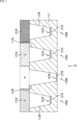
図1に示すように、表示素子1には、例えば、ガラス、シリコンウェハ、又は樹脂などよりなる基板11上に、複数の画素(サブ画素100R,100W,100G,100B)が、2次元状に配置されてなる表示領域23が形成される。また、この表示領域23の周辺には、映像表示用のドライバである信号線駆動回路21及び走査線駆動回路22が形成される。
As shown in FIG. 1, the display element 1 has a
表示領域23内には、画素駆動回路33が形成されている。図2は、画素駆動回路33の構成の例を示している。
A
図2に示すように、画素駆動回路33は、駆動トランジスタTr1及び書き込みトランジスタTr2と、その間のキャパシタ(保持容量)Csと、第1の電源ライン(Vcc)及び第2の電源ライン(GND)の間において、駆動トランジスタTr1に直列に接続された有機発光素子101(101R,101W,101G,101B)とを有するアクティブ型の駆動回路である。
As shown in FIG. 2, the
画素駆動回路33において、列方向には、信号線31が複数配置され、行方向には、走査線32が複数配置されている。各信号線31と各走査線32との交差点が、有機発光素子101R,101W,101G,101Bのいずれか1つを含むサブ画素100R,100W,100G,100Bに対応している。
In the
各信号線31は、信号線駆動回路21に接続され、この信号線駆動回路21から信号線31を介して書き込みトランジスタTr2のソース電極に画像信号が供給されるようになっている。各走査線32は、走査線駆動回路22と接続され、この走査線駆動回路22から走査線32を介して、書き込みトランジスタTr2のゲート電極に、走査信号が順次供給されるようになっている。
Each
図3は、表示領域23の平面構成の例を示している。図3において、表示領域23には、赤色(R)の光を発生するサブ画素100Rと、白色(W)の光を発生するサブ画素100Wと、緑色(G)の光を発生するサブ画素100Gと、青色(B)の光を発生するサブ画素100Bとが、順に全体として2次元状に形成されている。
Figure 3 shows an example of the planar configuration of the
なお、隣り合うサブ画素100R,100W,100G,100B(サブピクセル)の組み合わせが、1つの画素(ピクセル)10を構成している。すなわち、表示領域23は、複数の画素10が2次元状(行列状)に配列され、各画素10は、赤色(R)、白色(W)、緑色(G)、及び青色(B)の4つのサブ画素100から構成される。換言すれば、表示領域23においては、2次元状に配置される各画素10は、WRGB画素とされる。
Note that a combination of
(画素の構造)
ところで、有機EL表示素子において、画素を構成する各サブ画素の輝度を向上させるためには、サブ画素のサイズを変えることで、対応することが可能となる。しかしながら、画素のうちの特定のサブ画素のサイズを大きくして、発光面積を増大させる方法をとった場合には、画素ピッチが変わってしまうため、高精細化が困難となる。
(Pixel structure)
In an organic EL display element, the luminance of each sub-pixel constituting a pixel can be improved by changing the size of the sub-pixel. However, when the size of a specific sub-pixel in a pixel is increased to increase the light-emitting area, the pixel pitch is changed, making it difficult to achieve high definition.
具体的には、図4に示すように、4つのサブ画素900から構成される画素90において、サブ画素900Wの輝度を向上させるために、4つのサブ画素900のうち、サブ画素900Wにおける発光部の発光面積を増大させた構造を想定する。
Specifically, as shown in FIG. 4, in a
この構造においては、サブ画素900Wのみ、発光面積が増大しているため、サブ画素900Wの画素ピッチが、他のサブ画素900R,900G,900Bの画素ピッチと異なることになる。そして、このように、サブ画素900ごとに画素ピッチが変わってしまうと、高精細化が困難となるのは先に述べた通りである。
In this structure, the light-emitting area is increased only in
そこで、本技術では、画素10を構成するサブ画素100ごとに、発光部に対する光反射部(リフレクタ)の高さを調整することで、画素ピッチを変えずに、サブ画素100ごとの輝度を調整することができるようにする。以下、本技術を適用した画素の構造として、第1の実施の形態乃至第3の実施の形態の画素10の構造を順に説明する。
In this technology, the height of the light reflecting portion (reflector) relative to the light emitting portion is adjusted for each sub-pixel 100 constituting the
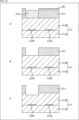
(画素の構造の第1の例)
図5は、第1の実施の形態の画素の構造の一部を示す要部断面図である。以下、この要部断面図を参照しながら、第1の実施の形態の画素10の構造を説明する。
(First Example of Pixel Structure)
5 is a cross-sectional view showing a part of the structure of a pixel according to the first embodiment. The structure of a
図5において、第1の実施の形態の画素10は、赤色(R)を発光するサブ画素100R、白色(W)を発光するサブ画素100W、緑色(G)を発光するサブ画素100G、及び青色(B)を発光するサブ画素100Bの4つのサブ画素から構成される。
In FIG. 5,
なお、サブ画素100Rは、有機発光素子101Rを含む。同様に、サブ画素100W,100G,100Bは、有機発光素子101W,101G,101Bをそれぞれ含んでいる。
Note that sub-pixel 100R includes organic light-emitting
有機発光素子101Rは、発光層を有する有機層と、電極から構成される発光部である。有機発光素子101Rにおいて、有機層は、アノード電極とカソード電極とに挟まれる構造からなるが、図5には、アノード電極121Rのみを図示している。なお、アノード電極121Rが露出した開口部は、発光部を規定するものとなる。
The organic light-emitting
ここで、有機層は、有機発光材料からなる発光層を有しているが、具体的には、例えば、正孔輸送層と発光層と電子輸送層との積層構造や、正孔輸送層と電子輸送層を兼ねた発光層との積層構造、正孔注入層と正孔輸送層と発光層と電子輸送層と電子注入層との積層構造などから構成することができる。例えば、この有機発光素子101Rは、白色に発光する構造を採用するのが望ましい。
Here, the organic layer has a light-emitting layer made of an organic light-emitting material, and specifically, for example, it can be composed of a laminated structure of a hole transport layer, a light-emitting layer, and an electron transport layer, a laminated structure of a hole transport layer and a light-emitting layer that also serves as an electron transport layer, or a laminated structure of a hole injection layer, a hole transport layer, a light-emitting layer, an electron transport layer, and an electron injection layer. For example, it is desirable to adopt a structure that emits white light for this organic light-emitting
また、サブ画素100Rにおいては、有機発光素子101Rに対して、透過光が赤色(R)の領域となるカラーフィルタ131Rが設けられており、これらの組み合わせによって、サブ画素100Rは、赤色(R)の光を発生する。
In addition, in the sub-pixel 100R, a
有機発光素子101Wは、有機発光素子101Rと同様に、有機層と電極(アノード電極121Wを含む)から構成される発光部である。有機発光素子101Wに対しては、カラーフィルタは設けられておらず、サブ画素100Wは、白色(W)の光を発生する。
Similar to the organic light-emitting
有機発光素子101Gは、有機発光素子101Rと同様に、有機層と電極(アノード電極121Gを含む)から構成される発光部である。有機発光素子101Gに対しては、透過光が緑色(G)の領域となるカラーフィルタ131Gが設けられており、これらの組み合わせによって、サブ画素100Gは、緑色(G)の光を発生する。
Like the organic light-emitting
有機発光素子101Bは、有機発光素子101Rと同様に、有機層と電極(アノード電極121Bを含む)から構成される発光部である。有機発光素子101Bに対しては、透過光が青色(B)の領域となるカラーフィルタ131Bが設けられており、これらの組み合わせによって、サブ画素100Bは、青色(B)の光を発生する。
Similar to organic light-emitting
また、第1の実施の形態の画素10は、光の取り出し効率を向上させるために、リフレクタ(光反射部)が設けられている。
In addition, the
ここで、リフレクタは、第1基板上に、有機発光素子からの光を表示面側に反射する第1部材と、第1基板に対向配置された第2基板と光反射構造との間を充填するとともに、第1部材の屈折率とは異なる屈折率を有する第2部材とから構成され、第1部材の表面において第2部材を伝播した光を反射させることによって、光取り出し効率を向上させることができる。 The reflector is composed of a first member that reflects light from the organic light-emitting element toward the display surface on the first substrate, and a second member that fills the space between the light reflecting structure and a second substrate that faces the first substrate and has a refractive index different from that of the first member. The light that has propagated through the second member is reflected at the surface of the first member, thereby improving the light extraction efficiency.
図5に示すように、第1の実施の形態の画素10おいては、光反射層(リフレクタ構造)として構成される第1部材111の表面に、リフレクタ112が形成されている。なお、第1部材111は、例えば、SiO2等の材料を用いて構成することができる。
5, in the
なお、ここでは、図示を省略しているが、第1の実施の形態の画素10においては、各有機発光素子101からの光を伝播して外部に射出する第2部材(例えば、後述の図17の第2部材151)が形成されており、その第2部材の間を充填するように、第1部材111が形成されている。すなわち、第1部材111と第2部材(例えば、後述の図17の第2部材151)によって、光反射層(リフレクタ構造)が形成されている。
Although not shown here, in the
ここで、図5に示すように、第1の実施の形態の画素10においては、サブ画素100R,サブ画素100W,サブ画素100G,及びサブ画素100Bの4つのサブ画素ごとに、リフレクタ112の高さ(第1部材111の斜面の高さ)が異なっている。
As shown in FIG. 5, in
ただし、第1部材111においては、アノード電極121が露出した開口部の側壁が、所定の傾斜角(リフレクタ角度)で傾斜しており、この斜面(表面)が、リフレクタ112を形成している。以下、この積層方向の斜面の高さを、リフレクタ112の「斜面高さ」ともいう。
However, in the
すなわち、第1の実施の形態の画素10において、各サブ画素100におけるリフレクタ112の斜面高さを比較した場合に、例えば、下記の式(1)に示すような関係とすることができる。
That is, when comparing the slope heights of the
リフレクタ112Wの斜面高さ > リフレクタ112Gの斜面高さ > リフレクタ112Rの斜面高さ > リフレクタ112Bの斜面高さ ・・・(1)
Slope height of
ただし、式(1)において、リフレクタ112Wの斜面高さは、サブ画素100Wにおける第1部材111の斜面の高さに相当する。同様に、リフレクタ112G,112R,112Bの斜面高さは、サブ画素100G,100R,100Bにおける第1部材111の斜面の高さに相当する。
However, in formula (1), the slope height of
このように、第1の実施の形態の画素10では、4つのサブ画素100ごとに、リフレクタ112の斜面高さを異なるようにして、サブ画素100ごとの輝度に差をつけることで、特定のサブ画素100の輝度を上げるようにしている。特に、サブ画素100Wのリフレクタ112Wの斜面高さを高くすることで、有機発光素子101W(アノード電極121W)からの光が全反射する領域が増加するため、サブ画素100Wの輝度が向上し、結果として、画素10全体の輝度を向上させることができる。
In this way, in the
また、第1の実施の形態の画素10では、各サブ画素100における発光面積やピッチ配列を変えずに、光を反射する領域、すなわち、リフレクタ112の斜面高さを変えることで、サブ画素100ごとの輝度に差をつけているため、高精細化を容易に行うことができる。
In addition, in the
以上、第1の実施の形態の画素10では、サブ画素100ごとに、発光部としての有機発光素子101(アノード電極121)に対するリフレクタ112の斜面高さを調整して、リフレクタ112Rと、リフレクタ112Wと、リフレクタ112Gと、リフレクタ112Bの斜面高さがそれぞれ異なるようにしている。これにより、第1の実施の形態の画素10においては、光反射層によって光の取り出し効率を向上させるだけでなく、サブ画素100ごとの輝度に差をつけて、特定のサブ画素100の輝度を向上させることが可能となる。
As described above, in the
なお、図5においては、上述した式(1)に示したように、リフレクタ112Wの斜面高さが最も高く、リフレクタ112G,リフレクタ112R,リフレクタ112Bの順に、その斜面高さが低くなっていく場合を例示したが、この式(1)に示した関係は一例であって、リフレクタ112R,112W,112G,112Bの斜面高さがそれぞれ異なっていればよく、その斜面高さの順序は任意である。
In FIG. 5, as shown in the above-mentioned formula (1), the slope height of
例えば、画素10において、サブ画素100ごとに寿命が異なる場合に、サブ画素100の輝度を向上させることで、印加電流密度を下げることができるため、各サブ画素100の寿命劣化を同一にする方向での調整を行うことができる。このような調整を行う場合に、例えば、下記の式(1)’に示すような関係を満たすように、サブ画素100ごとに、リフレクタ112の斜面高さを調整することができる。
For example, in a
リフレクタ112Bの斜面高さ > リフレクタ112Wの斜面高さ > リフレクタ112Gの斜面高さ > リフレクタ112Rの斜面高さ ・・・(1)’
Slope height of
また、図5においては、画素10を構成するサブ画素100が、図中の左側から右側に向かって、サブ画素100R,100W,100G,100Bの順に並んでいるが、これらのサブ画素100の並び順は任意である。さらに、図5に示したように、リフレクタ112の斜面高さは、サブ画素100Wのリフレクタ112Wのように均一な高さとなる場合だけでなく、均一な高さとならない場合も想定されるが、このような場合には、例えば、サブ画素100ごとに、リフレクタ112の斜面高さの平均値等を調整すればよい。
5, the sub-pixels 100 constituting the
(画素の構造の第2の例)
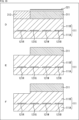
図6は、第2の実施の形態の画素の構造の一部を示す要部断面図である。以下、この要部断面図を参照しながら、第2の実施の形態の画素10の構造を説明する。
(Second Example of Pixel Structure)
6 is a cross-sectional view showing a part of the structure of a pixel according to the second embodiment. The structure of a
図6に示すように、第2の実施の形態の画素10においては、サブ画素100R,サブ画素100W,サブ画素100G,及びサブ画素100Bの4つのサブ画素100のうち、特定のサブ画素100のリフレクタ112の斜面高さが異なっている。
As shown in FIG. 6, in the
すなわち、第2の実施の形態の画素10(図6)は、上述した第1の実施の形態の画素10(図5)と比べて、4つのサブ画素100ごとに、リフレクタ112の斜面高さを変えるのではなく、4つのサブ画素100のうち、特定のサブ画素100のリフレクタ112の斜面高さを変えるようにしている。
In other words, in the
具体的には、図6においては、サブ画素100Wだけ、リフレクタ112Wの斜面高さを変えて、他のサブ画素100R,100G,100Bのリフレクタ112R,112G,112Bの斜面高さよりも、高くなるようにしている。
Specifically, in FIG. 6, the slope height of the
すなわち、第2の実施の形態の画素10において、各サブ画素100におけるリフレクタ112の斜面高さを比較した場合に、例えば、以下の式(2)に示すような関係とすることができる。
That is, when comparing the slope heights of the
リフレクタ112Wの斜面高さ > リフレクタ112Rの斜面高さ = リフレクタ112Gの斜面高さ = リフレクタ112Bの斜面高さ ・・・(2)
Slope height of
ただし、式(2)において、リフレクタ112Wの斜面高さは、サブ画素100Wにおける第1部材111の斜面の高さに相当する。同様に、リフレクタ112R,112G,112Bの斜面高さは、サブ画素100R,100G,100Bにおける第1部材111の斜面の高さに相当する。
However, in formula (2), the slope height of
このように、第2の実施の形態の画素10では、4つのサブ画素100のうち、特定のサブ画素100のリフレクタ112の斜面高さを異なるようにして、サブ画素100ごとの輝度に差をつけることで、特定のサブ画素100の輝度を上げることができる。例えば、サブ画素100Wのリフレクタ112Wのみ、その斜面高さを高くすることで、有機発光素子101W(アノード電極121W)からの光が全反射する領域が増加するため、サブ画素100Wの輝度が向上し、結果として、画素10全体の輝度を向上させることができる。
In this way, in the
また、第2の実施の形態の画素10においても、各サブ画素100の発光面積やピッチ配列を変えずに、リフレクタ112の斜面高さを変えることで、サブ画素100ごとの輝度に差をつけているため、高精細化を容易に行うことができる。
Also, in the
以上、第2の実施の形態の画素10では、サブ画素100ごとに、発光部としての有機発光素子101(アノード電極121)に対するリフレクタ112の斜面高さを調整して、特定のサブ画素100のリフレクタ112のみ、その斜面高さを、他のサブ画素100のリフレクタ112の斜面高さと異なるようにしている。これにより、第2の実施の形態の画素10においては、光反射層によって光の取り出し効率を向上させるだけでなく、サブ画素100ごとの輝度に差をつけて、特定のサブ画素100の輝度を向上させることが可能となる。
As described above, in the
なお、図6においては、上述した式(2)に示したように、リフレクタ112Wの斜面高さが最も高く、その他のリフレクタ112G,リフレクタ112R,リフレクタ112Bの斜面高さは同一の高さとなる場合を例示したが、この式(2)に示した関係は一例であって、特定のサブ画素100のリフレクタ112の斜面高さが、他のサブ画素100の斜面高さと異なっていればよく、どのリフレクタ112の斜面高さを変えるかは任意である。
Note that in FIG. 6, as shown in the above-mentioned formula (2), the slope height of
ここで、画素10において、サブ画素100ごとに寿命が異なる場合に、サブ画素100ごとに輝度を変化させることで、各サブ画素100の寿命劣化を同一にする方向での調整を行うことができるのは、先に述べた通りであるが、例えば、下記の式(2)’に示すような関係を満たすように、特定のサブ画素100Gのリフレクタ112Gの斜面高さを調整することができる。
Here, in a
リフレクタ112Bの斜面高さ > リフレクタ112Wの斜面高さ = リフレクタ112Gの斜面高さ = リフレクタ112Rの斜面高さ ・・・(2)’
Slope height of
さらに、ここでは、特定のサブ画素100として、1つのサブ画素100のリフレクタ112の斜面高さを変える場合を例示したが、例えば、サブ画素100W,100Bのリフレクタ112W,112Bの斜面高さを変えるなど、特定のサブ画素100の対象が、2以上のサブ画素100であってもよい。
Furthermore, while the example given here is of changing the slope height of the
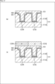
(画素の構造の第3の例)
図7は、第3の実施の形態の画素の構造の一部を示す要部断面図である。以下、この要部断面図を参照しながら、第3の実施の形態の画素10の構造を説明する。
(Third Example of Pixel Structure)
7 is a cross-sectional view showing a part of the structure of a pixel according to the third embodiment. The structure of a
図7に示すように、第3の実施の形態の画素10においては、サブ画素100R,サブ画素100W,サブ画素100G,及びサブ画素100Bの4つのサブ画素100のうち、特定のサブ画素100に含まれる有機発光素子101のアノード電極121の位置が調整されている。
As shown in FIG. 7, in the
すなわち、第3の実施の形態の画素10(図7)は、上述した第1の実施の形態の画素10(図5)及び第2の実施の形態の画素10(図6)と比べて、サブ画素100において、リフレクタ112の斜面高さ(積層方向の高さ)を調整するのではなく、有機発光素子101のアノード電極121の位置(積層方向の位置)を調整している。
That is, in the
このように、有機発光素子101(アノード電極121)側の位置を調整することでも、サブ画素100ごとに、発光部としての有機発光素子101(のアノード電極121)に対するリフレクタ112の斜面高さを調整することができる。その結果として、特定のサブ画素100のリフレクタ112の斜面高さを、他のサブ画素100のリフレクタ112の斜面高さと異なるようにすることができる。
In this way, by adjusting the position of the organic light-emitting element 101 (anode electrode 121), the slope height of the
具体的には、図7においては、サブ画素100Wだけ、有機発光素子101Wのアノード電極121Wの位置が、積層方向に深くなるように形成することで、サブ画素100Wのリフレクタ112Wの斜面高さが、他のサブ画素100R,100G,100Bのリフレクタ112R,112G,112Bの斜面高さよりも、高くなるようにしている。
Specifically, in FIG. 7, the position of the
すなわち、第3の実施の形態において、各サブ画素100におけるリフレクタ112の斜面高さを比較した場合には、例えば、上述した式(2)と同様の関係が得られる。
In other words, in the third embodiment, when comparing the slope heights of the
このように、第3の実施の形態の画素10では、4つのサブ画素100のうち、特定のサブ画素100の有機発光素子101のアノード電極121の位置を調整して、特定のサブ画素100のリフレクタ112の斜面高さを異なるようにすることで、サブ画素100ごとの輝度に差をつけることが可能となり、結果として、特定のサブ画素100の輝度を上げることができる。
In this way, in the
例えば、サブ画素100Wの有機発光素子101Wのアノード電極121Wの位置を調整して、サブ画素100Wのリフレクタ112Wのみ、その斜面高さを高くすることで、サブ画素100Wの輝度が向上し、結果として、画素10全体の輝度を向上させることができる。
For example, by adjusting the position of the
また、第3の実施の形態の画素10においても、各サブ画素100の発光面積やピッチ配列を変えずに、有機発光素子101のアノード電極121の位置を調整することで、サブ画素100ごとの輝度に差をつけているため、高精細化を容易に行うことができる。
Also, in the
以上、第3の実施の形態の画素10では、特定のサブ画素100のアノード電極121側の位置を調整することで、サブ画素100ごとに、発光部としての有機発光素子101のアノード電極121に対するリフレクタ112の斜面高さを調整して、特定のサブ画素100のリフレクタ112のみ、その斜面高さを、他のサブ画素100のリフレクタ112の斜面高さと異なるようにしている。これにより、第3の実施の形態の画素10においては、光反射層によって光の取り出し効率を向上させるだけでなく、サブ画素100ごとの輝度に差をつけて、特定のサブ画素100の輝度を向上させることが可能となる。
As described above, in the
なお、図7においては、上述した式(2)と同様の関係となるように、リフレクタ112Wの斜面高さが最も高く、その他のリフレクタ112G,リフレクタ112R,リフレクタ112Bの斜面高さは同一の高さとなる場合を例示したが、この関係は一例であって、特定のサブ画素100のリフレクタ112の斜面高さが、他のサブ画素100の斜面高さと異なっていればよく、どのサブ画素100のアノード電極121側の位置を調整するかは任意である。
Note that in FIG. 7, the slope height of
また、ここでは、特定のサブ画素100として、1つのサブ画素100のアノード電極121側の位置を調整する場合を提示したが、例えば、サブ画素100W,100Bのアノード電極121W,121B側の位置を調整するなど、特定のサブ画素100の対象が、2以上のサブ画素100であってもよい。さらに、画素10において、サブ画素100ごとに、アノード電極121側の位置を調整するようにして、例えば、上述した式(1)の関係を満たすようにしてもよい。
Although the case where the position of one
(リフレクタの構造の詳細)
次に、図8乃至図12を参照して、リフレクタ112の構造の詳細について説明する。
(Reflector structure details)
Next, the structure of the
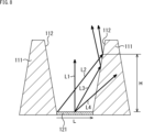
図8は、リフレクタ112による光の反射を説明する概念図である。
Figure 8 is a conceptual diagram explaining the reflection of light by the
図8に示すように、サブ画素100において、リフレクタ112に対する有機発光素子101(のアノード電極121)からの光は、全方位となるが、リフレクタ112では、所定の全反射の角度以上で入射してきた光は反射されるが、それ以下の角度で侵入してきた光は透過することになる。
As shown in FIG. 8, in the
例えば、図8において、有機発光素子101のアノード電極121からの光線L1乃至L4のうち、光線L2,L3は、リフレクタ112によって全反射される一方で、光線L4は、リフレクタ112を透過している。
For example, in FIG. 8, of the light rays L1 to L4 from the
ここで、図9には、リフレクタ112の斜面までの距離L(単位:nm)と、全反射するリフレクタ112の高さ(斜面高さ)H(単位:nm)との関係を示している。
Here, Figure 9 shows the relationship between the distance L (unit: nm) to the slope of the
例えば、リフレクタ112の間の開口部(アノード電極121が露出している部分)の幅が、2000nmとなる場合には、リフレクタ112の斜面までの距離Lは、最大で、2000nmとなる。この場合において、全反射条件を満たす高さHは、図9に示したLとHの関係から、略1600nmとなる。
For example, if the width of the opening between the reflectors 112 (the portion where the
すなわち、リフレクタ112において、反射領域は、高さH = 1600nm以上となり、この高さ(斜面高さ)Hを高くするほど、全反射領域が増加するため、サブ画素100の輝度を向上させることができる。換言すれば、高さ(斜面高さ)Hの増加に対して、反射面積の増加分で、輝度が向上すると言える。
That is, in the
ここで、全反射条件を満たす高さ(斜面高さ)Hは、例えば、次のような計算によって求めることができる。 Here, the height (slope height) H that satisfies the total reflection condition can be calculated, for example, as follows:
すなわち、図10に示すように、リフレクタ112に入射する光の入射角(反射角)をθとしたとき、αは、下記の式(3)によって、計算することができる。
That is, as shown in FIG. 10, when the angle of incidence (angle of reflection) of light incident on the
α = tan-1 (H / (L + t)) ・・・(3) α = tan -1 (H / (L + t)) ... (3)
ここで、リフレクタ角度(傾斜角)をβとすれば、三角形の外角の定理によって、下記の式(4)の関係が得られる。 If the reflector angle (tilt angle) is β, the exterior angle theorem of a triangle gives us the relationship in equation (4) below.
(90 - θ) + α = β ・・・(4) (90 - θ) + α = β ... (4)
したがって、上述の式(3)及び式(4)から、下記の式(5)の関係を導くことができる。 Therefore, from the above equations (3) and (4), the relationship in the following equation (5) can be derived.
θ = 90 + α - β = 90 + tan-1 (H / (L + t)) - β
tan-1 (H / (L + t)) = θ + β - 90
tan(θ + β - 90) = H / (L + t) ・・・(5)
θ = 90 + α - β = 90 + tan -1 (H / (L + t)) - β
tan -1 (H / (L + t)) = θ + β - 90
tan(θ + β - 90) = H / (L + t) ... (5)
また、tanβ = H/t の関係から、t = H/tanβが得られるので、上述の式(5)に基づき、下記の式(6)の関係を導くことができる。 In addition, from the relationship tanβ = H/t, we obtain t = H/tanβ, so based on the above equation (5), we can derive the relationship in the following equation (6).
H = (L + t) × tan(θ + β - 90) = (L + (H/tanβ)) × tan(θ + β - 90) ・・・(6) H = (L + t) × tan(θ + β - 90) = (L + (H/tanβ)) × tan(θ + β - 90) ・・・(6)
そして、θ > θmax(臨界角)で全反射するので、下記の式(7)の関係を満たす高さHを求めることができる。 Since total reflection occurs when θ>θ max (critical angle), it is possible to obtain the height H that satisfies the relationship of the following formula (7).
H ≧ L × tan(θmax + β - 90) / (1 - (tan(θmax + β - 90) / tanβ)) ・・・(7) H≧L × tan( θmax +β−90)/(1−(tan( θmax +β−90)/tanβ)) …(7)
このようにして、全反射条件を満たす高さ(斜面高さ)Hが求められる。 In this way, the height (slope height) H that satisfies the total reflection condition is determined.
ここで、図10に示すように、リフレクタ112(例えば、SiO)の屈折率nA、すなわち、第1部材111の表面の屈折率nAを1.4とし、リフレクタ112との界面における有機層(例えば、後述の図17の層141)の有機EL材料の屈折率nBを1.8とした場合を想定する。この場合において、全反射となるθmax(臨界角)は、下記の式(8)の関係を有する。
10, it is assumed that the refractive index nA of the reflector 112 (e.g., SiO), i.e., the refractive index nA of the surface of the
sinθmax = sinθmax / sin90°= nA / nB ・・・(8) sinθ max = sinθ max / sin90° = nA / nB ... (8)
そして、式(8)を計算することで、下記の式(9)の計算結果が得られる。 Then, by calculating equation (8), the calculation result of equation (9) below is obtained.
θmax = sin-1(nA / nB) = sin-1(1.4 / 1.8) = sin-1(0.882) = 51.3° ・・・(9) θ max = sin -1 (nA / nB) = sin -1 (1.4 / 1.8) = sin -1 (0.882) = 51.3° ... (9)
このようにして、θmax = 51.3°が得られるので、例えば、L = 1000nmで、β = 71°の場合を想定すれば、上述の式(7)に基づき、下記の式(10)を解くことで、H = 808nm を求めることができる。 In this way, θ max = 51.3° is obtained. For example, if we assume that L = 1000 nm and β = 71°, then H = 808 nm can be obtained by solving the following equation (10) based on the above equation (7).
H = L × tan(θmax + β - 90) / (1 - (tan(θmax + β - 90) / tanβ))
= 1000 × tan(51.3°+ 71°- 90°) / (1 - (tan(51.3°+ 71°- 90°) / tan71°))
= 808.07
H = L × tan(θ max + β - 90) / (1 - (tan(θ max + β - 90) / tanβ))
= 1000 × tan(51.3°+ 71°- 90°) / (1 - (tan(51.3°+ 71°- 90°) / tan71°))
= 808.07
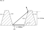
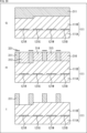
また、本技術の発明者は、リフレクタ角度βを変化させた場合の全反射条件を満たす高さ(斜面高さ)Hの変化を、詳細なるシミュレーションによって求めることで、最適なリフレクタ角度βと、リフレクタ112の間の開口部の幅(開口部分の大きさ)の分析を行った。このシミュレーションの結果を、図11に示している。 The inventors of this technology also conducted a detailed simulation to determine the change in height (slope height) H that satisfies the total reflection condition when the reflector angle β is changed, and analyzed the optimal reflector angle β and the width of the opening between the reflectors 112 (the size of the opening). The results of this simulation are shown in Figure 11.
図11の表は、リフレクタ角度βの値(単位:度)と、リフレクタ112の斜面までの距離Lの値(単位:nm)を、それぞれ変化させたときの全反射条件を満たす高さ(斜面高さ)Hの値(単位:nm)を示している。
The table in Figure 11 shows the value of the height (slope height) H (unit: nm) that satisfies the total reflection condition when the value of the reflector angle β (unit: degrees) and the value of the distance L (unit: nm) to the slope of the
ただし、図11の表においては、β = 60°,65°,68°,70°,71°,73°,74°,75°,80°とし、L = 10nm, 100nm, 500nm, 1000nm, 1500nm, 2000nm, 2500nm, 3000nmとしたときに、上述の式(7)を計算することで得られる高さHの値を示している。 However, the table in Figure 11 shows the values of height H obtained by calculating the above formula (7) when β = 60°, 65°, 68°, 70°, 71°, 73°, 74°, 75°, 80° and L = 10nm, 100nm, 500nm, 1000nm, 1500nm, 2000nm, 2500nm, 3000nm.
そして、このシミュレーションの結果から、発光部としての有機発光素子101が発光する部分(アノード電極121が露出している部分)の幅、すなわち、開口部分の大きさは、3000nm以下が望ましく、その場合のリフレクタ角度βは、60°~ 80°が望ましいことが見いだされた。このような全反射条件を満たす構造の例を、図12に示している。図12においては、β = 71°,L = 2000nmとしたときに、H =1616nmとなっている。
The results of this simulation showed that the width of the portion from which the organic light-emitting element 101 emits light (the portion where the
(製造工程の第1の例)
次に、図13乃至図17を参照して、本技術の実施の形態の画素の製造工程の第1の例の流れを説明する。
(First Example of Manufacturing Process)
Next, a flow of a first example of a manufacturing process for a pixel according to the embodiment of the present technology will be described with reference to FIGS.
なお、製造工程の第1の例では、説明の便宜上、画素10を構成する任意のサブ画素100として、サブ画素100R,100Gの製造工程の流れについて説明する。
In the first example of the manufacturing process, for the sake of convenience, the flow of the manufacturing process of sub-pixels 100R and 100G will be described as an
ここでは、まず、図13のAに示すように、ドライ加工工程が行われる。このドライ加工工程によって、第1部材111A上に、アノード電極121R,121Gが形成される。なお、第1部材111Aの材料としては、例えば、SiO2等を用いることができる。また、アノード電極121の材料としては、例えば、AlCu等を用いることができる。
Here, first, a dry processing step is performed as shown in A of Fig. 13. By this dry processing step,
次に、図13のBに示すように、CVD成膜工程が行われる。このCVD成膜工程によって、第1部材111A上に形成されたアノード電極121R,121Gに対し、第1部材111Bが成膜される。なお、第1部材111Bの材料としては、例えば、P-SiO等を用いることができる。
Next, as shown in FIG. 13B, a CVD film formation process is performed. Through this CVD film formation process, a
次に、図13のCに示すように、レジスト塗布工程が行われる。このレジスト塗布工程によって、第1部材111B上に、フォトレジスト211が塗布される。
Next, as shown in FIG. 13C, a resist coating process is performed. In this resist coating process,
続いて、図14のDに示すように、露光工程が行われる。この露光工程によって、フォトマスク221を用い、フォトレジスト211の表面をパターン状に露光することで、露光された部分(露光部分212)と、露光されていない部分(露光部分212を除いた部分)からなるパターンが形成される。
Next, as shown in FIG. 14D, an exposure process is performed. In this exposure process, a
次に、図14のEに示すように、現像工程が行われる。この現像工程によって、フォトレジスト211の露光部分212が除去される。
Next, as shown in FIG. 14E, a development process is performed. This development process removes the exposed
次に、図14のFに示すように、エッチング工程が行われる。このエッチング工程によって、フォトレジスト211によりマスクされた部分を除いた部分がエッチングされ、第1部材111Bの一部が加工される。
Next, as shown in FIG. 14F, an etching process is performed. This etching process etches the portions other than the portion masked by the
続いて、図15のGに示すように、レジスト塗布工程が行われる。このレジスト塗布工程によって、第1部材111Bの加工部分上にも、フォトレジスト211が塗布される。
Next, as shown in FIG. 15G, a resist coating process is performed. Through this resist coating process,
次に、図15のHに示すように、露光工程が行われる。この露光工程によって、フォトマスク231を用い、フォトレジスト211の表面をパターン状に露光することで、露光された部分(露光部分213,214)と、露光されていない部分(露光部分213,214を除いた部分)からなるパターンが形成される。
Next, as shown in FIG. 15H, an exposure process is performed. In this exposure process, a
次に、図15のIに示すように、現像工程が行われる。この現像工程によって、フォトレジスト211の露光部分213,214が除去される。
Next, as shown in I of FIG. 15, a development process is performed. This development process removes the exposed
続いて、図16のJに示すように、エッチング工程が行われる。このエッチング工程によって、フォトレジスト211によりマスクされた部分を除いた部分がエッチングされ、第1部材111Bの一部が加工される。この加工によって、サブ画素100ごとに高さが異なるリフレクタが形成され、第1部材111A上のアノード電極121R,121Gが露出する。
Then, as shown in FIG. 16J, an etching process is performed. In this etching process, the portions other than the portion masked by the
次に、図16のKに示すように、レジスト剥離工程が行われる。このレジスト剥離工程によって、フォトレジスト211が剥離される。
Next, as shown in FIG. 16K, a resist stripping process is performed. This resist stripping process strips the
次に、図16のLに示すように、蒸着工程とCVD成膜工程が行われる。この蒸着工程によって、第1部材111A上に形成されたアノード電極121R,121Gと、第1部材111Bの表面に、有機層及びカソード電極層からなる層141と、保護膜142が成膜される。なお、有機層は、アノード電極とカソード電極層との間で発光する。例えば、この有機層は、白色に発光する構造が望ましい。なお、保護膜142の材料としては、例えば、絶縁性材料又は導電性材料などを用いることができる。
Next, as shown in FIG. 16L, a vapor deposition process and a CVD film formation process are performed. Through this vapor deposition process, a
続いて、図17のMに示すように、平坦化工程が行われる。この平坦化工程によって、第2部材151が埋め込まれ、平坦化される。なお、この第2部材151の材料としては、例えば、アクリル系樹脂やポリミイド系樹脂、シリコン系樹脂等の樹脂などを用いることができる。
Next, as shown in M of FIG. 17, a planarization process is performed. In this planarization process, the
このように、有機層及びカソード電極層からなる層141と、保護膜142を形成したのち、さらに、第2部材151を形成することで、第1部材111(111B)と、第2部材151とからなる光反射層(リフレクタ構造)が形成される。
In this way, after forming the
次に、図17のNに示すように、カラーフィルタ形成工程が行われる。このカラーフィルタ形成工程によって、平坦化された第2部材151上に、カラーフィルタ131R,131Gが形成される。
Next, as shown in N of FIG. 17, a color filter formation process is performed. Through this color filter formation process,
以上のようにして製造される画素10においては、サブ画素100ごとに、第1部材111の斜面の傾斜によるリフレクタの斜面高さが異なっているため、サブ画素100ごとの輝度に差をつけて、特定のサブ画素100の輝度を向上させることが可能となる。
In the
以上、製造工程の第1の例を説明した。 The above describes the first example of the manufacturing process.
(製造工程の第2の例)
次に、図18乃至図22を参照して、本技術の実施の形態の画素の製造工程の第2の例の流れを説明する。
(Second Example of Manufacturing Process)
Next, a flow of a second example of the manufacturing process of a pixel according to the embodiment of the present technology will be described with reference to FIGS.
なお、製造工程の第2の例では、説明の便宜上、画素10を構成する任意のサブ画素100として、サブ画素100R,100G,100W,100Bの製造工程の流れについて説明する。
In the second example of the manufacturing process, for the sake of convenience, the flow of the manufacturing process of sub-pixels 100R, 100G, 100W, and 100B will be described as any sub-pixel 100 constituting a
ここでは、まず、図18のAに示すように、ドライ加工工程が行われる。このドライ加工工程によって、第1部材111A上に、アノード電極121R,121G,121W,121Bが形成される。なお、第1部材111Aの材料としては、例えば、SiO2等を用いることができる。また、アノード電極121の材料としては、例えば、AlCu等を用いることができる。
Here, first, a dry processing step is performed as shown in A of Fig. 18. By this dry processing step,
次に、図18のBに示すように、CVD成膜工程が行われる。このCVD成膜工程によって、第1部材111A上に形成されたアノード電極121R,121G,121W,121Bに対し、第1部材111Bが成膜される。なお、第1部材111Bの材料としては、例えば、P-SiO等を用いることができる。
Next, as shown in FIG. 18B, a CVD film formation process is performed. Through this CVD film formation process, a
次に、図18のCに示すように、レジスト塗布工程が行われる。このレジスト塗布工程によって、第1部材111B上に、フォトレジスト311が塗布される。
Next, as shown in FIG. 18C, a resist coating process is performed. In this resist coating process,
続いて、図19のDに示すように、露光工程が行われる。この露光工程によって、フォトマスク321を用い、フォトレジスト311の表面をパターン状に露光することで、露光された部分(露光部分312)と、露光されていない部分(露光部分312を除いた部分)からなるパターンが形成される。
Next, as shown in FIG. 19D, an exposure process is performed. In this exposure process, a
次に、図19のEに示すように、現像工程が行われる。この現像工程によって、フォトレジスト311の露光部分312が除去される。
Next, as shown in FIG. 19E, a development process is performed. This development process removes the exposed
次に、図19のFに示すように、エッチング工程が行われる。このエッチング工程によって、フォトレジスト311によりマスクされた部分を除いた部分がエッチングされ、第1部材111Bの一部が加工される。
Next, as shown in FIG. 19F, an etching process is performed. This etching process etches the portions other than the portion masked by the
続いて、図20のGに示すように、レジスト塗布工程が行われる。このレジスト塗布工程によって、第1部材111Bの加工部分上にも、フォトレジスト311が塗布される。
Next, as shown in FIG. 20G, a resist coating process is performed. Through this resist coating process,
次に、図20のHに示すように、露光工程が行われる。この露光工程によって、フォトマスク331を用い、フォトレジスト311の表面をパターン状に露光することで、露光された部分(露光部分313,314,315,316)と、露光されていない部分(露光部分313,314,315,316を除いた部分)からなるパターンが形成される。
Next, as shown in FIG. 20H, an exposure process is performed. In this exposure process, a
次に、図20のIに示すように、現像工程が行われる。この現像工程によって、フォトレジスト311の露光部分313,314,315,316が除去される。
Next, as shown in FIG. 20I, a development process is performed. This development process removes exposed
続いて、図21のJに示すように、エッチング工程が行われる。このエッチング工程によって、フォトレジスト311によりマスクされた部分を除いた部分がエッチングされ、第1部材111Bの一部が加工される。この加工によって、サブ画素100ごとに高さが異なるリフレクタが形成され、第1部材111A上のアノード電極121R,121G,121W,121Bが露出する。
Then, as shown in FIG. 21J, an etching process is performed. In this etching process, the portions other than the portion masked by the
次に、図21のKに示すように、レジスト剥離工程が行われる。このレジスト剥離工程によって、フォトレジスト311が剥離される。
Next, as shown in FIG. 21K, a resist stripping process is performed. This resist stripping process strips the
次に、図21のLに示すように、蒸着工程とCVD成膜工程が行われる。この蒸着工程によって、第1部材111A上に形成されたアノード電極121R,121G,121W,121Bと、第1部材111Bの表面に、有機層及びカソード電極層からなる層141と、保護膜142が成膜される。なお、有機層は、アノード電極とカソード電極層との間で発光する。例えば、この有機層は、白色に発光する構造が望ましい。なお、この保護膜142の材料としては、例えば、絶縁性材料又は導電性材料などを用いることができる。
Next, as shown in FIG. 21L, a vapor deposition process and a CVD film formation process are performed. Through this vapor deposition process, a
続いて、図22のMに示すように、平坦化工程が行われる。この平坦化工程によって、第2部材151が埋め込まれ、平坦化される。なお、この第2部材としては、例えば、アクリル系樹脂やポリミイド系樹脂、シリコン系樹脂等の樹脂などを用いることができる。
Next, as shown in FIG. 22M, a planarization process is performed. In this planarization process, the
このように、有機層及びカソード電極層からなる層141と、保護膜142を形成したのち、さらに、第2部材151を形成することで、第1部材111(111B)と、第2部材151とからなる光反射層(リフレクタ構造)が形成される。
In this way, after forming the
次に、図22のNに示すように、カラーフィルタ形成工程が行われる。このカラーフィルタ形成工程によって、平坦化された第2部材151上に、カラーフィルタ131R,131G,131Bが形成される。
Next, as shown in N of FIG. 22, a color filter formation process is performed. Through this color filter formation process,
以上のようにして製造される画素10においては、サブ画素100ごとに、第1部材111の斜面の傾斜によるリフレクタの斜面高さが異なっているため、サブ画素100ごとの輝度に差をつけて、特定のサブ画素100の輝度を向上させることが可能となる。
In the
以上、製造工程の第2の例を説明した。 The above describes the second example of the manufacturing process.
<2.変形例> <2. Modifications>
上述した実施の形態では、画素10が、WRGB画素、すなわち、4つのサブ画素100R,100G,100B,100Wから構成されるとして説明したが、サブ画素100の構成は、これに限定されるものではない。
In the above embodiment, the
例えば、画素10において、サブ画素100Wを設けずに、3つのサブ画素100R,100G,100Bから構成されるようにしてもよい。また、例えば、白色(W)のサブ画素100Wに代えて、白色(W)と同等に視感度の高い他の色のサブ画素100を用いてもよい。さらに、画素10において、複数のサブ画素100の並び順についても、色ごとに任意の順序に並べることができる。
For example, the
また、上述した第1,第2の実施の形態では、サブ画素100ごとに、リフレクタ112の斜面高さを調整する一方で、上述した第3の実施の形態では、サブ画素100ごとに、アノード電極121側の位置を調整していたが、それらの調整を同時に行ってもよい。すなわち、画素10において、サブ画素100ごとに、リフレクタ112の斜面高さと、アノード電極121側の位置の両方を調整するようにしてもよい。
In the first and second embodiments described above, the slope height of the
なお、上述した実施の形態において説明した各層の材料及び厚み、又は成膜方法及び成膜条件などは、上述の説明に限定されるものではなく、他の材料及び厚み、又は他の成膜方法及び成膜条件としてもよい。また、上述した実施の形態などでは、有機発光素子101の構成を具体的に説明したが、全ての層を有する必要はなく、また、他の層をさらに有するようにしてもよい。 The materials and thicknesses of each layer, or the film-forming methods and film-forming conditions, described in the above-mentioned embodiments are not limited to those described above, and other materials and thicknesses, or other film-forming methods and film-forming conditions may be used. In addition, in the above-mentioned embodiments, the configuration of the organic light-emitting element 101 is specifically described, but it is not necessary to have all layers, and other layers may be further included.
また、上述した実施の形態では、アクティブマトリックス型の表示素子(表示装置)の構成について説明したが、本技術は、パッシブマトリックス型の表示素子(表示装置)への適用も可能である。さらにまた、アクティブマトリックス駆動のための画素駆動回路の構成は、上述した実施の形態で説明したものに限らず、必要に応じて容量素子やトランジスタなどを適宜追加してもよい。その場合には、画素駆動回路の変更に応じて、上述の信号線駆動回路21(図1)や走査線駆動回路22(図1)のほかに、必要な駆動回路を適宜追加してもよい。 In addition, in the above-mentioned embodiment, the configuration of an active matrix type display element (display device) has been described, but the present technology can also be applied to a passive matrix type display element (display device). Furthermore, the configuration of the pixel drive circuit for active matrix driving is not limited to that described in the above-mentioned embodiment, and capacitive elements, transistors, etc. may be added as necessary. In that case, in addition to the above-mentioned signal line drive circuit 21 (Figure 1) and scanning line drive circuit 22 (Figure 1), necessary drive circuits may be added as necessary depending on the change in the pixel drive circuit.
<3.電子機器の例> <3. Examples of electronic devices>
(一眼レフカメラの例)
図23は、本技術を適用した表示素子が適用される電子機器(撮像装置)として、一眼レフカメラ(レンズ交換式一眼レフレックスタイプのデジタルカメラ)の外観の例を示している。
(Example of a single-lens reflex camera)
FIG. 23 shows an example of the external appearance of a single-lens reflex camera (a lens-interchangeable single-lens reflex type digital camera) as an electronic device (imaging device) to which a display element to which the present technology is applied is applied.
この一眼レフカメラは、図23のAに示すように、例えば、カメラ本体部(カメラボディ)411の正面右側に、交換式の撮影レンズユニット(交換レンズ)412を有し、正面左側に、撮影者が把持するためのグリップ部413を有している。
As shown in FIG. 23A, this single-lens reflex camera has, for example, an interchangeable photographing lens unit (interchangeable lens) 412 on the right side of the front of the camera main body (camera body) 411, and a
また、図23のBに示すように、カメラ本体部411の背面略中央部には、モニタ414が設けられている。モニタ414の上部には、ビューファインダ(接眼窓)415が設けられている。撮影者は、ビューファインダ415を覗くことによって、撮影レンズユニット412から導かれた被写体の光像を視認して構図決定を行うことが可能である。
As shown in FIG. 23B, a
このビューファインダ415は、上述した本技術を適用した表示素子(表示素子1)により構成されている。
This
(ヘッドマウントディスプレイの例)
図24は、本技術を適用した表示素子が適用される電子機器として、ヘッドマウントディスプレイ(HMD:Head Mounted Display)の外観の例を示している。
(Example of a head-mounted display)
FIG. 24 shows an example of the appearance of a head mounted display (HMD) as an electronic device to which a display element to which the present technology is applied is applied.
このヘッドマウントディスプレイは、図24のAに示すように、例えば、眼鏡型の表示部511の両側に、使用者の頭部に装着するための耳掛け部512を有している。この表示部511は、上述した本技術を適用した表示素子(表示素子1)により構成されている。
As shown in A of FIG. 24, this head mounted display has, for example, ear hooks 512 on both sides of a glasses-
例えば、図24のAのヘッドマウントディスプレイを頭部に装着したユーザは、表示部511に表示される、仮想現実(VR:Virtual Reality)の映像を見ることができる。
For example, a user wearing the head-mounted display of FIG. 24A on his/her head can view virtual reality (VR) images displayed on the
なお、図24のAでは、使用者の目を完全に覆った非透過型のヘッドマウントディスプレイの例を示したが、図24のBに示すように、透過型(例えばビデオ透過等)のヘッドマウントディスプレイの表示部521が、上述した本技術を適用した表示素子(表示素子1)により構成されるようにしてもよい。
Note that while A in FIG. 24 shows an example of a non-transmissive head-mounted display that completely covers the user's eyes, as shown in B in FIG. 24, the
例えば、図24のBのヘッドマウントディスプレイを頭部に装着したユーザは、表示部521に表示される拡張現実(AR:Augmented Reality)の映像を見ることができる。
For example, a user wearing the head-mounted display of FIG. 24B on his/her head can view an augmented reality (AR) image displayed on the
(その他の例)
なお、上述した図23及び図24においては、本技術を適用した表示素子が適用される電子機器として、一眼レフカメラとヘッドマウントディスプレイを例示したが、例えば、スマートフォン、テレビ受像機、パーソナルコンピュータ、ビデオカメラ、携帯電話機、ゲーム機、ウェアラブル機器などの電子機器に、本技術を適用した表示素子が適用されるようにしてもよい。
(Other examples)
In the above-mentioned Figures 23 and 24, a single-lens reflex camera and a head-mounted display are shown as examples of electronic devices to which the display element to which the present technology is applied can be applied. However, the display element to which the present technology is applied can also be applied to electronic devices such as smartphones, television sets, personal computers, video cameras, mobile phones, game consoles, and wearable devices.
また、本技術の実施の形態は、上述した実施の形態に限定されるものではなく、本技術の要旨を逸脱しない範囲において種々の変更が可能である。 Furthermore, the embodiments of this technology are not limited to the above-mentioned embodiments, and various modifications are possible without departing from the spirit of this technology.
また、本技術は、以下のような構成をとることができる。 This technology can also be configured as follows:
(1)
複数のサブ画素からなる画素を2次元状に配置した表示領域を有し、
前記画素は、前記サブ画素ごとに、発光部に対する光反射部の高さを調整している
表示素子。
(2)
前記サブ画素ごとに、前記光反射部の積層方向の斜面の高さを調整している
前記(1)に記載の表示素子。
(3)
前記サブ画素ごとに、前記光反射部の斜面の高さが異なる
前記(2)に記載の表示素子。
(4)
複数の前記サブ画素のうち、特定のサブ画素のみ、前記光反射部の斜面の高さが異なる
前記(2)に記載の表示素子。
(5)
前記サブ画素ごとに、前記発光部の積層方向の位置を調整している
前記(1)に記載の表示素子。
(6)
前記サブ画素ごとに、前記発光部の位置が異なる
前記(5)に記載の表示素子。
(7)
複数の前記サブ画素のうち、特定のサブ画素のみ、前記発光部の位置が異なる
前記(5)に記載の表示素子。
(8)
前記光反射部の斜面の高さは、前記光反射部の斜面の角度と、前記発光部の発光部分の幅に応じて調整される
前記(1)乃至(7)のいずれかに記載の表示素子。
(9)
前記画素は、3つの基本色光を発する第1のサブ画素、第2のサブ画素、及び第3のサブ画素と、非基本色光を発する第4のサブ画素からなる
前記(1)乃至(8)のいずれかに記載の表示素子。
(10)
前記基本色光は、赤色光、緑色光、及び青色光であり、
前記非基本色光は、白色光である
前記(9)に記載の表示素子。
(11)
前記サブ画素は、前記発光部として自発光する発光素子を有する画素であり、
前記発光素子は、電極と、発光層を有する有機層から構成される
前記(1)乃至(10)のいずれかに記載の表示素子。
(12)
複数のサブ画素からなる画素を2次元状に配置した表示領域を有し、
前記画素は、前記サブ画素ごとに、発光部に対する光反射部の高さを調整している
表示素子を備える電子機器。
(1)
A display area in which pixels each made up of a plurality of sub-pixels are arranged two-dimensionally,
The pixel includes a sub-pixel, and a height of a light reflecting portion relative to a light emitting portion is adjusted for each of the sub-pixels.
(2)
The display element according to (1), wherein a height of a slope of the light reflecting portion in the stacking direction is adjusted for each of the sub-pixels.
(3)
The display element according to (2), wherein the height of the inclined surface of the light reflecting portion differs for each of the sub-pixels.
(4)
The display element according to (2), wherein heights of the inclined surfaces of the light reflecting portions of only specific sub-pixels among the plurality of sub-pixels are different.
(5)
The display element according to (1), wherein a position of the light-emitting portion in a stacking direction is adjusted for each of the sub-pixels.
(6)
The display element according to (5), wherein the light-emitting portion is positioned differently for each of the sub-pixels.
(7)
The display element according to (5), wherein the positions of the light-emitting portions of only specific sub-pixels among the plurality of sub-pixels are different.
(8)
The display element according to any one of (1) to (7), wherein a height of the inclined surface of the light reflecting portion is adjusted depending on an angle of the inclined surface of the light reflecting portion and a width of a light emitting portion of the light emitting portion.
(9)
The display element according to any one of (1) to (8), wherein the pixel includes a first sub-pixel, a second sub-pixel, and a third sub-pixel that emit three basic color lights, and a fourth sub-pixel that emits a non-basic color light.
(10)
the primary color lights are red light, green light, and blue light;
The display element according to (9), wherein the non-basic color light is white light.
(11)
the sub-pixel is a pixel having a light-emitting element that emits light by itself as the light-emitting portion,
The display element according to any one of (1) to (10), wherein the light-emitting element is constituted by an electrode and an organic layer having a light-emitting layer.
(12)
A display area in which pixels each made up of a plurality of sub-pixels are arranged two-dimensionally,
The electronic device comprising: a display element, wherein the pixel includes a light reflecting portion having a height adjusted with respect to a light emitting portion for each of the sub-pixels.
1 表示素子, 10 画素, 11 基板, 21 信号線駆動回路, 22 走査線駆動回路, 23 表示領域, 31 信号線, 32 走査線, 33 画素駆動回路, 100,100R,100G,100B,100W サブ画素, 101,101R,101G,101B,101W 有機発光素子, 111 第1部材, 112,112R,112G,112B,112W リフレクタ, 121,121R,121G,121B,121W アノード電極, 131,131R,131G,131B カラーフィルタ, 141 層, 142 保護膜, 151 第2部材 1 Display element, 10 Pixel, 11 Substrate, 21 Signal line driving circuit, 22 Scanning line driving circuit, 23 Display area, 31 Signal line, 32 Scanning line, 33 Pixel driving circuit, 100, 100R, 100G, 100B, 100W Subpixel, 101, 101R, 101G, 101B, 101W Organic light-emitting element, 111 First member, 112, 112R, 112G, 112B, 112W Reflector, 121, 121R, 121G, 121B, 121W Anode electrode, 131, 131R, 131G, 131B Color filter, 141 Layer, 142 Protective film, 151 Second member
Claims (4)
前記第1のサブ画素は、第1のアノード電極を含む第1の有機発光素子を有し、
前記第2のサブ画素は、第2のアノード電極を含む第2の有機発光素子を有し、
前記画素は、
無機材料からなる第1の部材を有し、
前記第1の部材は、前記第1の有機発光素子からの光を反射する第1の反射面と、前記第2の有機発光素子からの光を反射する第2の反射面を形成しており、
前記第1のアノード電極の下面から、前記第1の反射面を形成した前記第1の部材の上面までの積層方向の距離である第1の距離と、前記第2のアノード電極の下面から、前記第2の反射面を形成した前記第1の部材の上面までの積層方向の距離である第2の距離とが異なり、
前記第1の部材は、
前記第1のアノード電極が露出した第1の開口部に対する側壁が、所定の傾斜角で傾斜して前記第1の反射面を形成し、
前記第2のアノード電極が露出した第2の開口部に対する側壁が、所定の傾斜角で傾斜して前記第2の反射面を形成し、
前記第1のアノード電極の少なくとも一部の領域は、前記第1の反射面を形成する側壁と接し、
前記第2のアノード電極の少なくとも一部の領域は、前記第2の反射面を形成する側壁と接し、
前記画素における前記第1のサブ画素と前記第2のサブ画素は、発光面積と画素ピッチが同じである
表示素子。 a display region in which pixels including a first sub-pixel that emits a first light and a second sub-pixel that emits a second light different from the first light are arranged two-dimensionally;
The first sub-pixel has a first organic light-emitting element including a first anode electrode;
the second sub-pixel has a second organic light-emitting element including a second anode electrode;
The pixel is
A first member made of an inorganic material is provided,
the first member forms a first reflecting surface that reflects light from the first organic light-emitting element and a second reflecting surface that reflects light from the second organic light-emitting element;
a first distance, which is a distance in a stacking direction from a lower surface of the first anode electrode to an upper surface of the first member forming the first reflecting surface, is different from a second distance, which is a distance in a stacking direction from a lower surface of the second anode electrode to an upper surface of the first member forming the second reflecting surface ;
The first member includes:
a side wall of the first opening through which the first anode electrode is exposed is inclined at a predetermined inclination angle to form the first reflecting surface;
a side wall of the second opening through which the second anode electrode is exposed is inclined at a predetermined inclination angle to form the second reflecting surface;
At least a portion of the first anode electrode is in contact with a sidewall that forms the first reflecting surface,
At least a portion of the second anode electrode is in contact with a sidewall that forms the second reflecting surface,
The first sub-pixel and the second sub-pixel in the pixel have the same light-emitting area and pixel pitch.
Display element.
前記第1の屈折率と異なる第2の屈折率を有する第2の部材であって、前記第1の開口部から露出した前記第1のアノード電極及び前記第1の反射面による第1の凹部と、前記第2の開口部から露出した前記第2のアノード電極及び前記第2の反射面による第2の凹部に埋め込まれた前記第2の部材と
により光反射層が形成される
請求項1に記載の表示素子。 the first member having a first refractive index;
2. The display element according to claim 1, wherein a light reflecting layer is formed by a second member having a second refractive index different from the first refractive index, the second member being embedded in a first recess formed by the first anode electrode and the first reflective surface exposed from the first opening, and a second recess formed by the second anode electrode and the second reflective surface exposed from the second opening.
第3のアノード電極を含む第3の有機発光素子を有し、前記第1の光、及び前記第2の光と異なる第3の光を発する第3のサブ画素と、
第4のアノード電極を含む第4の有機発光素子を有し、前記第1の光、前記第2の光、及び前記第3の光と異なる第4の光を発する第4のサブ画素と
をさらに含み、
前記画素における前記第1のサブ画素と、前記第2のサブ画素と、前記第3のサブ画素と、前記第4のサブ画素は、発光面積と画素ピッチが同じであり、
前記第1の部材は、前記第3の有機発光素子からの光を反射する第3の反射面と、前記第4の有機発光素子からの光を反射する第4の反射面をさらに形成しており、
前記第3のアノード電極の下面から、前記第3の反射面を形成した前記第1の部材の上面までの積層方向の距離である第3の距離と、前記第4のアノード電極の下面から、前記第4の反射面を形成した前記第1の部材の上面までの積層方向の距離である第4の距離は、前記第1の距離及び前記第2の距離の少なくとも一方と異なり、
前記第1の部材は、
前記第3のアノード電極が露出した第3の開口部に対する側壁が、所定の傾斜角で傾斜して前記第3の反射面を形成し、
前記第4のアノード電極が露出した第4の開口部に対する側壁が、所定の傾斜角で傾斜して前記第4の反射面を形成し、
前記第3のアノード電極の少なくとも一部の領域は、前記第3の反射面を形成する側壁と接し、
前記第4のアノード電極の少なくとも一部の領域は、前記第4の反射面を形成する側壁と接する
請求項1に記載の表示素子。 The pixel is
a third sub-pixel having a third organic light-emitting element including a third anode electrode, the third sub-pixel emitting a third light different from the first light and the second light;
a fourth sub-pixel having a fourth organic light-emitting element including a fourth anode electrode, the fourth sub-pixel emitting a fourth light different from the first light, the second light, and the third light,
the first sub-pixel, the second sub-pixel, the third sub-pixel, and the fourth sub-pixel in the pixel have the same light-emitting area and pixel pitch;
the first member further forms a third reflecting surface that reflects light from the third organic light-emitting element and a fourth reflecting surface that reflects light from the fourth organic light-emitting element;
a third distance, which is a distance in a stacking direction from a lower surface of the third anode electrode to an upper surface of the first member forming the third reflecting surface, and a fourth distance, which is a distance in a stacking direction from a lower surface of the fourth anode electrode to an upper surface of the first member forming the fourth reflecting surface, are different from at least one of the first distance and the second distance,
The first member includes:
a side wall of the third opening through which the third anode electrode is exposed is inclined at a predetermined inclination angle to form the third reflecting surface;
a side wall of the fourth opening through which the fourth anode electrode is exposed is inclined at a predetermined inclination angle to form the fourth reflecting surface;
At least a portion of the third anode electrode is in contact with a sidewall that forms the third reflecting surface,
At least a portion of the fourth anode electrode is in contact with a sidewall that forms the fourth reflecting surface.
The display device according to claim 1 .
前記第1のサブ画素は、第1のアノード電極を含む第1の有機発光素子を有し、
前記第2のサブ画素は、第2のアノード電極を含む第2の有機発光素子を有し、
前記画素は、
無機材料からなる第1の部材を有し、
前記第1の部材は、前記第1の有機発光素子からの光を反射する第1の反射面と、前記第2の有機発光素子からの光を反射する第2の反射面を形成しており、
前記第1のアノード電極の下面から、前記第1の反射面を形成した前記第1の部材の上面までの積層方向の距離である第1の距離と、前記第2のアノード電極の下面から、前記第2の反射面を形成した前記第1の部材の上面までの積層方向の距離である第2の距離とが異なり、
前記第1の部材は、
前記第1のアノード電極が露出した第1の開口部に対する側壁が、所定の傾斜角で傾斜して前記第1の反射面を形成し、
前記第2のアノード電極が露出した第2の開口部に対する側壁が、所定の傾斜角で傾斜して前記第2の反射面を形成し、
前記第1のアノード電極の少なくとも一部の領域は、前記第1の反射面を形成する側壁と接し、
前記第2のアノード電極の少なくとも一部の領域は、前記第2の反射面を形成する側壁と接し、
前記画素における前記第1のサブ画素と前記第2のサブ画素は、発光面積と画素ピッチが同じである
表示素子を備える電子機器。 a display region in which pixels including a first sub-pixel that emits a first light and a second sub-pixel that emits a second light different from the first light are arranged two-dimensionally;
The first sub-pixel has a first organic light-emitting element including a first anode electrode;
the second sub-pixel has a second organic light-emitting element including a second anode electrode;
The pixel is
A first member made of an inorganic material is provided,
the first member forms a first reflecting surface that reflects light from the first organic light-emitting element and a second reflecting surface that reflects light from the second organic light-emitting element;
a first distance, which is a distance in a stacking direction from a lower surface of the first anode electrode to an upper surface of the first member forming the first reflecting surface, is different from a second distance, which is a distance in a stacking direction from a lower surface of the second anode electrode to an upper surface of the first member forming the second reflecting surface ;
The first member includes:
a side wall of the first opening through which the first anode electrode is exposed is inclined at a predetermined inclination angle to form the first reflecting surface;
a side wall of the second opening through which the second anode electrode is exposed is inclined at a predetermined inclination angle to form the second reflecting surface;
At least a portion of the first anode electrode is in contact with a sidewall that forms the first reflecting surface,
At least a portion of the second anode electrode is in contact with a sidewall that forms the second reflecting surface,
The first sub-pixel and the second sub-pixel in the pixel have the same light-emitting area and pixel pitch.
An electronic device equipped with a display element.
Priority Applications (1)
| Application Number | Priority Date | Filing Date | Title |
|---|---|---|---|
| JP2023012555A JP7463577B2 (en) | 2017-12-26 | 2023-01-31 | Display element and electronic device |
Applications Claiming Priority (2)
| Application Number | Priority Date | Filing Date | Title |
|---|---|---|---|
| JP2017248697A JP2019114484A (en) | 2017-12-26 | 2017-12-26 | Display element and electronic device |
| JP2023012555A JP7463577B2 (en) | 2017-12-26 | 2023-01-31 | Display element and electronic device |
Related Parent Applications (1)
| Application Number | Title | Priority Date | Filing Date |
|---|---|---|---|
| JP2017248697A Division JP2019114484A (en) | 2017-12-26 | 2017-12-26 | Display element and electronic device |
Publications (2)
| Publication Number | Publication Date |
|---|---|
| JP2023055824A JP2023055824A (en) | 2023-04-18 |
| JP7463577B2 true JP7463577B2 (en) | 2024-04-08 |
Family
ID=65023970
Family Applications (2)
| Application Number | Title | Priority Date | Filing Date |
|---|---|---|---|
| JP2017248697A Pending JP2019114484A (en) | 2017-12-26 | 2017-12-26 | Display element and electronic device |
| JP2023012555A Active JP7463577B2 (en) | 2017-12-26 | 2023-01-31 | Display element and electronic device |
Family Applications Before (1)
| Application Number | Title | Priority Date | Filing Date |
|---|---|---|---|
| JP2017248697A Pending JP2019114484A (en) | 2017-12-26 | 2017-12-26 | Display element and electronic device |
Country Status (6)
| Country | Link |
|---|---|
| US (2) | US11569483B2 (en) |
| EP (1) | EP3732739A1 (en) |
| JP (2) | JP2019114484A (en) |
| KR (2) | KR20250035026A (en) |
| CN (3) | CN111512460B (en) |
| WO (1) | WO2019131487A1 (en) |
Families Citing this family (4)
| Publication number | Priority date | Publication date | Assignee | Title |
|---|---|---|---|---|
| KR102890077B1 (en) * | 2019-08-02 | 2025-11-24 | 삼성디스플레이 주식회사 | Display device and method of manufacturing for display device |
| CN112133734B (en) * | 2020-09-29 | 2022-08-30 | 湖北长江新型显示产业创新中心有限公司 | Display panel and display device |
| TWI771896B (en) | 2021-02-04 | 2022-07-21 | 錼創顯示科技股份有限公司 | Micro light-emitting diode display panel |
| CN112786766B (en) * | 2021-02-04 | 2023-05-16 | 錼创显示科技股份有限公司 | Micro light-emitting diode display panel |
Citations (12)
| Publication number | Priority date | Publication date | Assignee | Title |
|---|---|---|---|---|
| JP2006278257A (en) | 2005-03-30 | 2006-10-12 | Sony Corp | Organic light emitting device and method for manufacturing the same |
| JP2007503093A (en) | 2003-08-19 | 2007-02-15 | イーストマン コダック カンパニー | OLED device with microcavity gamut subpixel |
| JP2007248484A (en) | 2006-03-13 | 2007-09-27 | Sony Corp | Display device |
| JP2009049135A (en) | 2007-08-17 | 2009-03-05 | Sony Corp | Display device |
| JP2009206041A (en) | 2008-02-29 | 2009-09-10 | Sony Corp | Organic light-emitting device and its manufacturing method |
| JP2010056017A (en) | 2008-08-29 | 2010-03-11 | Fujifilm Corp | Color display device and method of manufacturing the same |
| US20120176025A1 (en) | 2011-01-10 | 2012-07-12 | Samsung Mobile Display Co., Ltd. | Organic Light Emitting Display Apparatus and Method of Manufacturing the Same |
| JP2013191533A (en) | 2012-02-17 | 2013-09-26 | Sony Corp | Display device and manufacturing method therefor |
| WO2014148263A1 (en) | 2013-03-21 | 2014-09-25 | ソニー株式会社 | Display device, method for manufacturing same, and electronic device |
| US20140332762A1 (en) | 2013-05-13 | 2014-11-13 | Samsung Display Co., Ltd. | Organic electroluminescent display |
| WO2016158074A1 (en) | 2015-04-01 | 2016-10-06 | ソニー株式会社 | Display device, display device production method, and electronic device |
| WO2017051622A1 (en) | 2015-09-25 | 2017-03-30 | ソニー株式会社 | Display device and method for manufacturing same |
Family Cites Families (24)
| Publication number | Priority date | Publication date | Assignee | Title |
|---|---|---|---|---|
| JP4693253B2 (en) * | 2001-01-30 | 2011-06-01 | 株式会社半導体エネルギー研究所 | Light emitting device, electronic equipment |
| US7129634B2 (en) * | 2004-04-07 | 2006-10-31 | Eastman Kodak Company | Color OLED with added color gamut pixels |
| JP4192837B2 (en) * | 2004-04-30 | 2008-12-10 | セイコーエプソン株式会社 | Display element and method for manufacturing display element |
| KR20100066416A (en) * | 2007-09-06 | 2010-06-17 | 소니 가부시끼가이샤 | Optical extraction element, method for manufacturing the optical extraction element, and display device |
| JP2009110873A (en) * | 2007-10-31 | 2009-05-21 | Toppan Printing Co Ltd | Display device |
| JP5258412B2 (en) * | 2008-06-24 | 2013-08-07 | キヤノン株式会社 | LIGHT EMITTING ELEMENT, DISPLAY DEVICE USING LIGHT EMITTING ELEMENT AND LIGHT EMITTING ELEMENT MANUFACTURING METHOD |
| WO2010143360A1 (en) * | 2009-06-11 | 2010-12-16 | パナソニック株式会社 | Organic el display |
| JP2014225323A (en) * | 2011-09-12 | 2014-12-04 | シャープ株式会社 | Light-emitting device, display device, and illuminating device |
| JP5927476B2 (en) * | 2011-10-03 | 2016-06-01 | 株式会社Joled | Display device and electronic device |
| US9281451B2 (en) * | 2012-02-17 | 2016-03-08 | Industrial Technology Research Institute | Light emitting element and fabricating method thereof |
| KR101990116B1 (en) * | 2012-10-22 | 2019-10-01 | 삼성디스플레이 주식회사 | Organic light emitting device and manufacture method thereof |
| TWI674671B (en) * | 2013-05-28 | 2019-10-11 | 日商新力股份有限公司 | Display device and electronic device |
| JP6191287B2 (en) * | 2013-07-05 | 2017-09-06 | ソニー株式会社 | Display device |
| JP2016081562A (en) * | 2014-10-09 | 2016-05-16 | ソニー株式会社 | Display device, display device manufacturing method, and electronic apparatus |
| JP5918340B2 (en) * | 2014-11-25 | 2016-05-18 | ユー・ディー・シー アイルランド リミテッド | Color display device and manufacturing method thereof |
| CN105070739B (en) * | 2015-08-17 | 2018-06-01 | 京东方科技集团股份有限公司 | Show backboard and preparation method thereof, display device |
| JP2017067999A (en) * | 2015-09-30 | 2017-04-06 | セイコーエプソン株式会社 | Substrate for electro-optic device, electro-optic device and electronic apparatus |
| JP6727848B2 (en) * | 2016-02-26 | 2020-07-22 | 株式会社ジャパンディスプレイ | Display device |
| EP3240036B1 (en) * | 2016-04-29 | 2024-05-01 | LG Display Co., Ltd. | Organic light-emitting display device and method of manufacturing the same |
| KR102525501B1 (en) * | 2016-05-23 | 2023-04-24 | 엘지디스플레이 주식회사 | Organic light emitting display device |
| JP7229777B2 (en) * | 2016-06-03 | 2023-02-28 | コーニング インコーポレイテッド | Light extraction devices and methods for OLED displays and OLED displays using them |
| JP6715708B2 (en) * | 2016-07-08 | 2020-07-01 | 株式会社ジャパンディスプレイ | Display device |
| US10141377B2 (en) * | 2016-07-29 | 2018-11-27 | Lg Display Co., Ltd. | Electroluminescent display device |
| CN108400154B (en) * | 2018-04-11 | 2019-12-24 | 武汉华星光电半导体显示技术有限公司 | OLED panel |
-
2017
- 2017-12-26 JP JP2017248697A patent/JP2019114484A/en active Pending
-
2018
- 2018-12-21 CN CN201880082731.1A patent/CN111512460B/en active Active
- 2018-12-21 US US16/955,917 patent/US11569483B2/en active Active
- 2018-12-21 CN CN202410983917.1A patent/CN118922014A/en active Pending
- 2018-12-21 KR KR1020257006365A patent/KR20250035026A/en active Pending
- 2018-12-21 KR KR1020207017496A patent/KR102775402B1/en active Active
- 2018-12-21 WO PCT/JP2018/047187 patent/WO2019131487A1/en not_active Ceased
- 2018-12-21 CN CN202410983931.1A patent/CN118922015A/en active Pending
- 2018-12-21 EP EP18834078.0A patent/EP3732739A1/en active Pending
-
2023
- 2023-01-31 JP JP2023012555A patent/JP7463577B2/en active Active
- 2023-02-01 US US17/987,269 patent/US20230292543A1/en active Pending
Patent Citations (12)
| Publication number | Priority date | Publication date | Assignee | Title |
|---|---|---|---|---|
| JP2007503093A (en) | 2003-08-19 | 2007-02-15 | イーストマン コダック カンパニー | OLED device with microcavity gamut subpixel |
| JP2006278257A (en) | 2005-03-30 | 2006-10-12 | Sony Corp | Organic light emitting device and method for manufacturing the same |
| JP2007248484A (en) | 2006-03-13 | 2007-09-27 | Sony Corp | Display device |
| JP2009049135A (en) | 2007-08-17 | 2009-03-05 | Sony Corp | Display device |
| JP2009206041A (en) | 2008-02-29 | 2009-09-10 | Sony Corp | Organic light-emitting device and its manufacturing method |
| JP2010056017A (en) | 2008-08-29 | 2010-03-11 | Fujifilm Corp | Color display device and method of manufacturing the same |
| US20120176025A1 (en) | 2011-01-10 | 2012-07-12 | Samsung Mobile Display Co., Ltd. | Organic Light Emitting Display Apparatus and Method of Manufacturing the Same |
| JP2013191533A (en) | 2012-02-17 | 2013-09-26 | Sony Corp | Display device and manufacturing method therefor |
| WO2014148263A1 (en) | 2013-03-21 | 2014-09-25 | ソニー株式会社 | Display device, method for manufacturing same, and electronic device |
| US20140332762A1 (en) | 2013-05-13 | 2014-11-13 | Samsung Display Co., Ltd. | Organic electroluminescent display |
| WO2016158074A1 (en) | 2015-04-01 | 2016-10-06 | ソニー株式会社 | Display device, display device production method, and electronic device |
| WO2017051622A1 (en) | 2015-09-25 | 2017-03-30 | ソニー株式会社 | Display device and method for manufacturing same |
Also Published As
| Publication number | Publication date |
|---|---|
| KR20250035026A (en) | 2025-03-11 |
| KR102775402B1 (en) | 2025-03-05 |
| EP3732739A1 (en) | 2020-11-04 |
| CN118922015A (en) | 2024-11-08 |
| CN118922014A (en) | 2024-11-08 |
| WO2019131487A1 (en) | 2019-07-04 |
| KR20200094755A (en) | 2020-08-07 |
| CN111512460B (en) | 2024-08-06 |
| US20210074954A1 (en) | 2021-03-11 |
| US20230292543A1 (en) | 2023-09-14 |
| JP2023055824A (en) | 2023-04-18 |
| US11569483B2 (en) | 2023-01-31 |
| JP2019114484A (en) | 2019-07-11 |
| CN111512460A (en) | 2020-08-07 |
Similar Documents
| Publication | Publication Date | Title |
|---|---|---|
| JP7463577B2 (en) | Display element and electronic device | |
| CN111916480B (en) | Display device and electronic apparatus | |
| CN108922916B (en) | Light emitting device and electronic apparatus | |
| US12349536B2 (en) | Electro-optical device and electronic apparatus | |
| JP7047811B2 (en) | Display devices and electronic devices | |
| JP2023052370A (en) | Display devices and electronic devices | |
| JP2017073268A (en) | Organic el device, method of manufacturing organic el device, and electronic apparatus | |
| JP6696193B2 (en) | Electro-optical device and electronic device | |
| CN111261791B (en) | Display device | |
| JP7711781B2 (en) | Display device and electronic device | |
| US11342538B2 (en) | Organic EL display device having reflection transmission portion, and electronic apparatus | |
| WO2020145148A1 (en) | Display device | |
| JP2018088381A (en) | Organic el device and manufacturing method of organic el device | |
| JP6318693B2 (en) | Display device and electronic device | |
| CN112289943B (en) | Light emitting devices and electronic equipment | |
| CN111244138A (en) | Electroluminescent display device | |
| WO2022124401A1 (en) | Display apparatus and electronic device | |
| CN112289944B (en) | Light emitting device and electronic apparatus | |
| US20250089540A1 (en) | Display device, method for manufacturing the same, and electronic apparatus | |
| JP2024126259A (en) | Display devices and electronic devices |
Legal Events
| Date | Code | Title | Description |
|---|---|---|---|
| A521 | Request for written amendment filed |
Free format text: JAPANESE INTERMEDIATE CODE: A523 Effective date: 20230228 |
|
| A621 | Written request for application examination |
Free format text: JAPANESE INTERMEDIATE CODE: A621 Effective date: 20230228 |
|
| A977 | Report on retrieval |
Free format text: JAPANESE INTERMEDIATE CODE: A971007 Effective date: 20231030 |
|
| A131 | Notification of reasons for refusal |
Free format text: JAPANESE INTERMEDIATE CODE: A131 Effective date: 20231107 |
|
| A521 | Request for written amendment filed |
Free format text: JAPANESE INTERMEDIATE CODE: A523 Effective date: 20240104 |
|
| TRDD | Decision of grant or rejection written | ||
| A01 | Written decision to grant a patent or to grant a registration (utility model) |
Free format text: JAPANESE INTERMEDIATE CODE: A01 Effective date: 20240227 |
|
| A61 | First payment of annual fees (during grant procedure) |
Free format text: JAPANESE INTERMEDIATE CODE: A61 Effective date: 20240327 |
|
| R150 | Certificate of patent or registration of utility model |
Ref document number: 7463577 Country of ref document: JP Free format text: JAPANESE INTERMEDIATE CODE: R150 |