JP5927476B2 - Display device and electronic device - Google Patents
Display device and electronic device Download PDFInfo
- Publication number
- JP5927476B2 JP5927476B2 JP2011219054A JP2011219054A JP5927476B2 JP 5927476 B2 JP5927476 B2 JP 5927476B2 JP 2011219054 A JP2011219054 A JP 2011219054A JP 2011219054 A JP2011219054 A JP 2011219054A JP 5927476 B2 JP5927476 B2 JP 5927476B2
- Authority
- JP
- Japan
- Prior art keywords
- sub
- pixels
- pixel
- display device
- width
- Prior art date
- Legal status (The legal status is an assumption and is not a legal conclusion. Google has not performed a legal analysis and makes no representation as to the accuracy of the status listed.)
- Active
Links
- 238000002834 transmittance Methods 0.000 claims description 102
- 239000000758 substrate Substances 0.000 claims description 77
- 239000011159 matrix material Substances 0.000 claims description 66
- 239000003086 colorant Substances 0.000 claims description 36
- 238000007789 sealing Methods 0.000 claims description 22
- 230000005540 biological transmission Effects 0.000 claims description 14
- 230000007935 neutral effect Effects 0.000 claims description 12
- 230000007423 decrease Effects 0.000 claims description 8
- 230000003247 decreasing effect Effects 0.000 claims 1
- 239000010410 layer Substances 0.000 description 65
- 238000005401 electroluminescence Methods 0.000 description 62
- 238000006243 chemical reaction Methods 0.000 description 29
- 238000012545 processing Methods 0.000 description 25
- 239000010408 film Substances 0.000 description 21
- 238000000034 method Methods 0.000 description 18
- 230000008859 change Effects 0.000 description 16
- 230000004048 modification Effects 0.000 description 16
- 238000012986 modification Methods 0.000 description 16
- 238000010586 diagram Methods 0.000 description 13
- 229910052751 metal Inorganic materials 0.000 description 12
- 239000000463 material Substances 0.000 description 11
- 239000002184 metal Substances 0.000 description 11
- 229910052721 tungsten Inorganic materials 0.000 description 9
- 239000004973 liquid crystal related substance Substances 0.000 description 8
- 239000003990 capacitor Substances 0.000 description 7
- 230000000694 effects Effects 0.000 description 7
- 239000012044 organic layer Substances 0.000 description 7
- 239000000956 alloy Substances 0.000 description 5
- 229910045601 alloy Inorganic materials 0.000 description 5
- 229910021417 amorphous silicon Inorganic materials 0.000 description 5
- 238000002347 injection Methods 0.000 description 5
- 239000007924 injection Substances 0.000 description 5
- 239000011810 insulating material Substances 0.000 description 5
- 229920006395 saturated elastomer Polymers 0.000 description 5
- 230000000052 comparative effect Effects 0.000 description 4
- 238000013461 design Methods 0.000 description 4
- 239000011777 magnesium Substances 0.000 description 4
- 230000008569 process Effects 0.000 description 4
- 229910052727 yttrium Inorganic materials 0.000 description 4
- PXHVJJICTQNCMI-UHFFFAOYSA-N Nickel Chemical compound [Ni] PXHVJJICTQNCMI-UHFFFAOYSA-N 0.000 description 3
- XLOMVQKBTHCTTD-UHFFFAOYSA-N Zinc monoxide Chemical compound [Zn]=O XLOMVQKBTHCTTD-UHFFFAOYSA-N 0.000 description 3
- 229910052782 aluminium Inorganic materials 0.000 description 3
- XAGFODPZIPBFFR-UHFFFAOYSA-N aluminium Chemical compound [Al] XAGFODPZIPBFFR-UHFFFAOYSA-N 0.000 description 3
- 239000004020 conductor Substances 0.000 description 3
- 239000011521 glass Substances 0.000 description 3
- 230000005525 hole transport Effects 0.000 description 3
- 229910044991 metal oxide Inorganic materials 0.000 description 3
- 150000004706 metal oxides Chemical class 0.000 description 3
- 230000035699 permeability Effects 0.000 description 3
- 239000000049 pigment Substances 0.000 description 3
- BASFCYQUMIYNBI-UHFFFAOYSA-N platinum Chemical compound [Pt] BASFCYQUMIYNBI-UHFFFAOYSA-N 0.000 description 3
- 230000001681 protective effect Effects 0.000 description 3
- 239000010409 thin film Substances 0.000 description 3
- 238000003079 width control Methods 0.000 description 3
- UHXOHPVVEHBKKT-UHFFFAOYSA-N 1-(2,2-diphenylethenyl)-4-[4-(2,2-diphenylethenyl)phenyl]benzene Chemical compound C=1C=C(C=2C=CC(C=C(C=3C=CC=CC=3)C=3C=CC=CC=3)=CC=2)C=CC=1C=C(C=1C=CC=CC=1)C1=CC=CC=C1 UHXOHPVVEHBKKT-UHFFFAOYSA-N 0.000 description 2
- BQCADISMDOOEFD-UHFFFAOYSA-N Silver Chemical compound [Ag] BQCADISMDOOEFD-UHFFFAOYSA-N 0.000 description 2
- 239000011575 calcium Substances 0.000 description 2
- 239000011651 chromium Substances 0.000 description 2
- 239000010949 copper Substances 0.000 description 2
- ZUOUZKKEUPVFJK-UHFFFAOYSA-N diphenyl Chemical compound C1=CC=CC=C1C1=CC=CC=C1 ZUOUZKKEUPVFJK-UHFFFAOYSA-N 0.000 description 2
- 230000001747 exhibiting effect Effects 0.000 description 2
- 239000010931 gold Substances 0.000 description 2
- 238000005259 measurement Methods 0.000 description 2
- 239000000203 mixture Substances 0.000 description 2
- 230000003287 optical effect Effects 0.000 description 2
- 230000002093 peripheral effect Effects 0.000 description 2
- 239000011241 protective layer Substances 0.000 description 2
- 229920005989 resin Polymers 0.000 description 2
- 239000011347 resin Substances 0.000 description 2
- VYPSYNLAJGMNEJ-UHFFFAOYSA-N silicon dioxide Inorganic materials O=[Si]=O VYPSYNLAJGMNEJ-UHFFFAOYSA-N 0.000 description 2
- 229910052709 silver Inorganic materials 0.000 description 2
- 239000004332 silver Substances 0.000 description 2
- NCGICGYLBXGBGN-UHFFFAOYSA-N 3-morpholin-4-yl-1-oxa-3-azonia-2-azanidacyclopent-3-en-5-imine;hydrochloride Chemical compound Cl.[N-]1OC(=N)C=[N+]1N1CCOCC1 NCGICGYLBXGBGN-UHFFFAOYSA-N 0.000 description 1
- 239000004925 Acrylic resin Substances 0.000 description 1
- 229920000178 Acrylic resin Polymers 0.000 description 1
- OYPRJOBELJOOCE-UHFFFAOYSA-N Calcium Chemical compound [Ca] OYPRJOBELJOOCE-UHFFFAOYSA-N 0.000 description 1
- VYZAMTAEIAYCRO-UHFFFAOYSA-N Chromium Chemical compound [Cr] VYZAMTAEIAYCRO-UHFFFAOYSA-N 0.000 description 1
- RYGMFSIKBFXOCR-UHFFFAOYSA-N Copper Chemical compound [Cu] RYGMFSIKBFXOCR-UHFFFAOYSA-N 0.000 description 1
- FYYHWMGAXLPEAU-UHFFFAOYSA-N Magnesium Chemical compound [Mg] FYYHWMGAXLPEAU-UHFFFAOYSA-N 0.000 description 1
- 239000004642 Polyimide Substances 0.000 description 1
- XUIMIQQOPSSXEZ-UHFFFAOYSA-N Silicon Chemical compound [Si] XUIMIQQOPSSXEZ-UHFFFAOYSA-N 0.000 description 1
- 230000009471 action Effects 0.000 description 1
- 239000012790 adhesive layer Substances 0.000 description 1
- 229910003481 amorphous carbon Inorganic materials 0.000 description 1
- 235000010290 biphenyl Nutrition 0.000 description 1
- 239000004305 biphenyl Substances 0.000 description 1
- 230000000903 blocking effect Effects 0.000 description 1
- 229910052791 calcium Inorganic materials 0.000 description 1
- 229910052804 chromium Inorganic materials 0.000 description 1
- 230000000295 complement effect Effects 0.000 description 1
- 229910052802 copper Inorganic materials 0.000 description 1
- 238000012937 correction Methods 0.000 description 1
- VBVAVBCYMYWNOU-UHFFFAOYSA-N coumarin 6 Chemical compound C1=CC=C2SC(C3=CC4=CC=C(C=C4OC3=O)N(CC)CC)=NC2=C1 VBVAVBCYMYWNOU-UHFFFAOYSA-N 0.000 description 1
- 230000005684 electric field Effects 0.000 description 1
- 238000000295 emission spectrum Methods 0.000 description 1
- 239000011888 foil Substances 0.000 description 1
- PCHJSUWPFVWCPO-UHFFFAOYSA-N gold Chemical compound [Au] PCHJSUWPFVWCPO-UHFFFAOYSA-N 0.000 description 1
- 229910052737 gold Inorganic materials 0.000 description 1
- 229910052749 magnesium Inorganic materials 0.000 description 1
- 239000012528 membrane Substances 0.000 description 1
- 150000002739 metals Chemical class 0.000 description 1
- YPJRZWDWVBNDIW-MBALSZOMSA-N n,n-diphenyl-4-[(e)-2-[4-[4-[(e)-2-[4-(n-phenylanilino)phenyl]ethenyl]phenyl]phenyl]ethenyl]aniline Chemical group C=1C=C(N(C=2C=CC=CC=2)C=2C=CC=CC=2)C=CC=1/C=C/C(C=C1)=CC=C1C(C=C1)=CC=C1\C=C\C(C=C1)=CC=C1N(C=1C=CC=CC=1)C1=CC=CC=C1 YPJRZWDWVBNDIW-MBALSZOMSA-N 0.000 description 1
- 229910052759 nickel Inorganic materials 0.000 description 1
- 150000004767 nitrides Chemical class 0.000 description 1
- 229920003986 novolac Polymers 0.000 description 1
- 238000001579 optical reflectometry Methods 0.000 description 1
- 239000004033 plastic Substances 0.000 description 1
- 229920003023 plastic Polymers 0.000 description 1
- 229910052697 platinum Inorganic materials 0.000 description 1
- 229920001721 polyimide Polymers 0.000 description 1
- 238000011112 process operation Methods 0.000 description 1
- 239000010453 quartz Substances 0.000 description 1
- 230000006798 recombination Effects 0.000 description 1
- 238000005215 recombination Methods 0.000 description 1
- 238000005070 sampling Methods 0.000 description 1
- 239000004065 semiconductor Substances 0.000 description 1
- 229910052710 silicon Inorganic materials 0.000 description 1
- 239000010703 silicon Substances 0.000 description 1
- HBMJWWWQQXIZIP-UHFFFAOYSA-N silicon carbide Chemical compound [Si+]#[C-] HBMJWWWQQXIZIP-UHFFFAOYSA-N 0.000 description 1
- HQVNEWCFYHHQES-UHFFFAOYSA-N silicon nitride Chemical compound N12[Si]34N5[Si]62N3[Si]51N64 HQVNEWCFYHHQES-UHFFFAOYSA-N 0.000 description 1
- 239000002356 single layer Substances 0.000 description 1
- 125000005504 styryl group Chemical group 0.000 description 1
- 239000000126 substance Substances 0.000 description 1
- WFKWXMTUELFFGS-UHFFFAOYSA-N tungsten Chemical compound [W] WFKWXMTUELFFGS-UHFFFAOYSA-N 0.000 description 1
- 239000010937 tungsten Substances 0.000 description 1
- XLYOFNOQVPJJNP-UHFFFAOYSA-N water Substances O XLYOFNOQVPJJNP-UHFFFAOYSA-N 0.000 description 1
- 239000011787 zinc oxide Substances 0.000 description 1
Images


Classifications
-
- H—ELECTRICITY
- H10—SEMICONDUCTOR DEVICES; ELECTRIC SOLID-STATE DEVICES NOT OTHERWISE PROVIDED FOR
- H10K—ORGANIC ELECTRIC SOLID-STATE DEVICES
- H10K59/00—Integrated devices, or assemblies of multiple devices, comprising at least one organic light-emitting element covered by group H10K50/00
- H10K59/30—Devices specially adapted for multicolour light emission
- H10K59/35—Devices specially adapted for multicolour light emission comprising red-green-blue [RGB] subpixels
- H10K59/351—Devices specially adapted for multicolour light emission comprising red-green-blue [RGB] subpixels comprising more than three subpixels, e.g. red-green-blue-white [RGBW]
-
- H—ELECTRICITY
- H10—SEMICONDUCTOR DEVICES; ELECTRIC SOLID-STATE DEVICES NOT OTHERWISE PROVIDED FOR
- H10K—ORGANIC ELECTRIC SOLID-STATE DEVICES
- H10K50/00—Organic light-emitting devices
- H10K50/80—Constructional details
- H10K50/86—Arrangements for improving contrast, e.g. preventing reflection of ambient light
- H10K50/865—Arrangements for improving contrast, e.g. preventing reflection of ambient light comprising light absorbing layers, e.g. light-blocking layers
-
- H—ELECTRICITY
- H10—SEMICONDUCTOR DEVICES; ELECTRIC SOLID-STATE DEVICES NOT OTHERWISE PROVIDED FOR
- H10K—ORGANIC ELECTRIC SOLID-STATE DEVICES
- H10K59/00—Integrated devices, or assemblies of multiple devices, comprising at least one organic light-emitting element covered by group H10K50/00
- H10K59/30—Devices specially adapted for multicolour light emission
- H10K59/38—Devices specially adapted for multicolour light emission comprising colour filters or colour changing media [CCM]
-
- H—ELECTRICITY
- H10—SEMICONDUCTOR DEVICES; ELECTRIC SOLID-STATE DEVICES NOT OTHERWISE PROVIDED FOR
- H10K—ORGANIC ELECTRIC SOLID-STATE DEVICES
- H10K59/00—Integrated devices, or assemblies of multiple devices, comprising at least one organic light-emitting element covered by group H10K50/00
- H10K59/80—Constructional details
- H10K59/87—Passivation; Containers; Encapsulations
- H10K59/871—Self-supporting sealing arrangements
-
- H—ELECTRICITY
- H10—SEMICONDUCTOR DEVICES; ELECTRIC SOLID-STATE DEVICES NOT OTHERWISE PROVIDED FOR
- H10K—ORGANIC ELECTRIC SOLID-STATE DEVICES
- H10K59/00—Integrated devices, or assemblies of multiple devices, comprising at least one organic light-emitting element covered by group H10K50/00
- H10K59/80—Constructional details
- H10K59/8791—Arrangements for improving contrast, e.g. preventing reflection of ambient light
- H10K59/8792—Arrangements for improving contrast, e.g. preventing reflection of ambient light comprising light absorbing layers, e.g. black layers
-
- H—ELECTRICITY
- H10—SEMICONDUCTOR DEVICES; ELECTRIC SOLID-STATE DEVICES NOT OTHERWISE PROVIDED FOR
- H10K—ORGANIC ELECTRIC SOLID-STATE DEVICES
- H10K50/00—Organic light-emitting devices
- H10K50/80—Constructional details
- H10K50/84—Passivation; Containers; Encapsulations
- H10K50/841—Self-supporting sealing arrangements
Description
本開示は、1つのピクセル(画素)に、例えば赤(R),緑(G),青(B),白(W)の4色のサブピクセル(サブ画素)が用いられた表示装置、およびそのような表示装置を備えた電子機器に関する。 The present disclosure relates to a display device in which, for example, four sub-pixels (sub-pixels) of red (R), green (G), blue (B), and white (W) are used for one pixel (pixel), and The present invention relates to an electronic device provided with such a display device.
複数の画素を有する表示装置においてカラー映像表示を行う場合、最も一般的な手法は、R(赤),G(緑),B(青)の3原色に対応する3つのサブ画素を各画素内に配置し、各サブ画素での輝度レベルを個別に調整するというものである。これにより、画素全体としての色度点および輝度を任意に設定することが可能となり、カラー映像表示が実現される。 When color image display is performed in a display device having a plurality of pixels, the most common method is that three sub-pixels corresponding to three primary colors of R (red), G (green), and B (blue) are included in each pixel. And the luminance level in each sub-pixel is individually adjusted. Thereby, it is possible to arbitrarily set the chromaticity point and the luminance of the entire pixel, and a color video display is realized.
このようなカラー映像表示が可能な表示装置の一例として、液晶表示装置が挙げられる。液晶表示装置は一般に、白色光を照射するバックライトと液晶表示パネルとを備えている。液晶表示パネルでは、通常、サブ画素ごとにR,G,Bの各色のカラーフィルタが設けられると共に、入射側および出射側のそれぞれに偏光板が貼り合わせられている。このため、バックライトからの照射光の強度が、偏光板およびカラーフィルタにおいて低減し、液晶表示装置全体での光利用効率が低下してしまう。これは、液晶表示装置において大幅なエネルギーロスとなり、消費電力の増大を招く。 As an example of a display device capable of displaying such a color image, a liquid crystal display device can be given. A liquid crystal display device generally includes a backlight that emits white light and a liquid crystal display panel. In a liquid crystal display panel, color filters of R, G, and B are usually provided for each subpixel, and polarizing plates are bonded to the incident side and the emission side, respectively. For this reason, the intensity | strength of the irradiation light from a backlight will reduce in a polarizing plate and a color filter, and the light utilization efficiency in the whole liquid crystal display device will fall. This causes a significant energy loss in the liquid crystal display device and causes an increase in power consumption.
そこで、低消費電力化を図るため、液晶表示パネルにおける各画素に4色のサブ画素を用いた構造が提案されている(例えば、特許文献1参照)。具体的には、上記したR,G,Bの3色のサブ画素に加え、これらの3色よりも高輝度を示す白(W)や黄(Y)などのサブピクセルを用いて映像表示を行い、これにより輝度効率を向上させて、低消費電力化を図っている。 Therefore, in order to reduce power consumption, a structure using sub-pixels of four colors for each pixel in a liquid crystal display panel has been proposed (for example, see Patent Document 1). Specifically, in addition to the above-described three sub-pixels of R, G, and B, video display is performed using sub-pixels such as white (W) and yellow (Y) that have higher luminance than these three colors. Thus, the luminance efficiency is improved and the power consumption is reduced.
このような4色のサブ画素を用いた表示装置としては、上記した液晶表示装置の他にも、有機EL(Electro Luminescence)表示装置が挙げられる(例えば、特許文献2〜5)。
As a display device using such four-color sub-pixels, an organic EL (Electro Luminescence) display device can be cited in addition to the liquid crystal display device described above (for example,
上記4色のサブ画素を有する有機EL表示装置では、各サブ画素に白色有機EL素子が用いられることが多い。このため、R,G,Bのサブ画素には、白色光から各色光を選択的に取り出すためのカラーフィルタが設けられる一方で、Wのサブ画素には、カラーフィルタが設けられず、白色発光素子から発せられた白色光が直接取り出されるようになっている。このような4色のサブ画素を用いて例えば映像表示を行う場合、高画質化を実現するためには、例えばR,G,Bの3色のサブ画素のみを用いる場合とは異なる、新たな輝度調整あるいは色度設計が要求される。 In the organic EL display device having the four color sub-pixels, a white organic EL element is often used for each sub-pixel. For this reason, the R, G, and B sub-pixels are provided with a color filter for selectively extracting each color light from white light, while the W sub-pixel is not provided with a color filter and emits white light. White light emitted from the element is directly extracted. When, for example, video display is performed using such four-color sub-pixels, a new image that is different from the case of using only three-color sub-pixels of R, G, and B, for example, is required in order to achieve high image quality. Brightness adjustment or chromaticity design is required.
本開示はかかる問題点に鑑みてなされたもので、その目的は、4色のサブ画素を用いて映像表示を行う際に、高画質化を実現することが可能な表示装置および電子機器を提供することにある。 The present disclosure has been made in view of such a problem, and an object thereof is to provide a display device and an electronic apparatus capable of realizing high image quality when video display is performed using four-color sub-pixels. There is to do.
本開示の第1の表示装置は、各々が、赤(R),緑(G),青(B)の各色に対応する第1ないし第3のサブ画素と、第1ないし第3のサブ画素よりも高輝度を示す第4のサブ画素とを有する複数の画素と、第1ないし第4のサブ画素のそれぞれに対向して第1ないし第4の開口を有するブラックマトリクスとを備えている。複数の画素ではそれぞれ、第1ないし第4のサブ画素が、対向配置された一対の基板間に有機電界発光素子を有し、ブラックマトリクスでは、第1ないし第3の開口に、R,G,Bの各色に対応するカラーフィルタが設けられ、第1ないし第4の開口の各形状は、有機電界発光素子の画素電極の基板面に平行な面形状よりも大きく、第4の開口の幅は、第1ないし第3の開口の幅よりも狭く、かつ第4の開口の幅と画素電極の幅との差は、第1ないし第3の開口のそれぞれの幅と画素電極の幅との差よりも小さいものである。
本開示の第2の表示装置は、各々が、赤(R),緑(G),青(B)の各色に対応する第1ないし第3のサブ画素と、第1ないし第3のサブ画素よりも高輝度を示す第4のサブ画素とを有する複数の画素と、第1ないし第4のサブ画素のそれぞれに対向して第1ないし第4の開口を有するブラックマトリクスとを備えている。複数の画素ではそれぞれ、第1ないし第4のサブ画素が、対向配置された一対の基板間に有機電界発光素子を有し、ブラックマトリクスでは、第1ないし第3の開口に、R,G,Bの各色に対応するカラーフィルタが設けられ、第4の開口には、中央部よりも端部においてより低透過率となるように構成された減光フィルタ(Neutral Density filter)が設けられている。
The first display device of the present disclosure includes first to third sub-pixels and first to third sub-pixels, each corresponding to each color of red (R), green (G), and blue (B). A plurality of pixels having a fourth sub-pixel exhibiting higher brightness, and a black matrix having first to fourth openings facing each of the first to fourth sub-pixels . In each of the plurality of pixels, the first to fourth sub-pixels each have an organic electroluminescent element between a pair of substrates arranged to face each other. In the black matrix, R, G, A color filter corresponding to each color of B is provided, each shape of the first to fourth openings is larger than a surface shape parallel to the substrate surface of the pixel electrode of the organic electroluminescent element, and the width of the fourth opening is The difference between the width of the fourth opening and the width of the pixel electrode is smaller than the width of the first to third openings, and the width of the pixel electrode is the difference between the width of each of the first to third openings and the width of the pixel electrode. Smaller than that.
According to the second display device of the present disclosure, the first to third subpixels and the first to third subpixels each corresponding to each color of red (R), green (G), and blue (B). A plurality of pixels having a fourth sub-pixel exhibiting higher brightness, and a black matrix having first to fourth openings facing each of the first to fourth sub-pixels. In each of the plurality of pixels, the first to fourth sub-pixels each have an organic electroluminescent element between a pair of substrates arranged to face each other. In the black matrix, R, G, A color filter corresponding to each color of B is provided, and a neutral density filter configured to have a lower transmittance at the end than at the center is provided at the fourth opening. .
本開示の第1の電子機器は、上記本開示の第1の表示装置を備えたものである。
本開示の第2の電子機器は、上記本開示の第2の表示装置を備えたものである。
A first electronic device of the present disclosure includes the first display device of the present disclosure.
A second electronic device of the present disclosure includes the second display device of the present disclosure.
本開示の第1の表示装置および電子機器、ならびに本開示の第2の表示装置および電子機器では、各画素が、R,G,Bに対応する第1ないし第3のサブ画素と、これら3つのサブ画素よりも高輝度を示す第4のサブ画素とを有し、第1ないし第3のサブ画素にはカラーフィルタが設けられている。第4のサブ画素において、有機電界発光素子から発せられた光の透過率が、その一部または全部において低減され、カラーフィルタを有する第1ないし第3のサブ画素と高輝度の第4のサブ画素との間の透過率差が軽減される。これにより、輝度バランスが良好となり、所望の色度を表現し易くなる。 In the first display device and electronic device of the present disclosure, and the second display device and electronic device of the present disclosure , each pixel includes first to third sub-pixels corresponding to R, G, and B, and 3 A fourth sub-pixel having higher luminance than one sub-pixel, and a color filter is provided in each of the first to third sub-pixels. In the fourth sub-pixel, the transmittance of light emitted from the organic electroluminescent element is reduced in part or in whole, and the first to third sub-pixels having a color filter and the high-luminance fourth sub-pixel. The difference in transmittance between the pixels is reduced. As a result, the luminance balance becomes good and the desired chromaticity is easily expressed.
例えば、一対の基板として、画素駆動回路を有する駆動基板と、透明基板よりなる封止基板とが設けられ、これらのうちの封止基板側にカラーフィルタが設けられている場合には、次のような構成となっていることが望ましい。即ち、カラーフィルタが、ブラックマトリクスの第1ないし第3のサブ画素に対向する開口にそれぞれ設けられ、第4のサブ画素では、ブラックマトリクスの開口幅が、他のサブ画素における各開口幅よりも小さくなっている。第4のサブ画素では、上記開口のエッジ部分における白色光のけられ(ケラレ)が、他のサブ画素よりも多く生じ、特に斜め方向へ出射する光の透過率が低減される。ここで、上記のようなサブ画素間における透過率差は視野角変化に伴って大きくなる傾向を有するが、そのような開口幅制御を行うことにより、特に斜め方向からみた場合に、所望の色度を表現し易くなる。 For example, as a pair of substrates, a drive substrate having a pixel drive circuit and a sealing substrate made of a transparent substrate are provided, and when a color filter is provided on the sealing substrate side of these, It is desirable to have such a configuration. That is, a color filter is provided in each of the openings facing the first to third sub-pixels of the black matrix, and in the fourth sub-pixel, the opening width of the black matrix is larger than each opening width in the other sub-pixels. It is getting smaller. In the fourth sub-pixel, white light vignetting (vignetting) occurs at the edge portion of the opening more than other sub-pixels, and in particular, the transmittance of light emitted in an oblique direction is reduced. Here, the transmittance difference between the sub-pixels as described above tends to increase as the viewing angle changes. However, by performing such aperture width control, a desired color can be obtained particularly when viewed from an oblique direction. It becomes easy to express degree.
本開示の第1の表示装置および電子機器、ならびに本開示の第2の表示装置および電子機器によれば、各画素が、R,G,Bに対応するカラーフィルタを有する第1ないし第3のサブ画素と、これら3つのサブ画素よりも高輝度を示す第4のサブ画素とを有している。第4のサブ画素において、有機電界発光素子から発せられた光の透過率が、その一部または全部において低減され、第1ないし第3のサブ画素と第4のサブ画素との間の透過率差を軽減でき、所望の色度を表現することができる。よって、4色のサブ画素を用いて映像表示を行う際に、高画質化を実現することが可能となる。 The first display device and the electronic apparatus of the present disclosure, as well as according to the second display device and the electronic apparatus of the present disclosure, each pixel is first to have a Luke color filter to correspond to R, G, and B 3 sub-pixels, and a fourth sub-pixel having higher luminance than these three sub-pixels. The in 4 sub-pixel, the transmittance of light emitted from the organic electroluminescent device, is reduced in a part or whole, the transmittance between the first to third sub-pixel and the fourth sub-pixel The difference can be reduced and desired chromaticity can be expressed. Therefore, it is possible to realize high image quality when performing video display using sub-pixels of four colors.
以下、本開示の実施の形態について、図面を参照して詳細に説明する。なお、説明は以下の順序で行う。
1.第1の実施の形態(BM開口を、RGBよりもWのサブ画素において小さくした例)2.第2の実施の形態(Wのサブ画素にNDフィルタを設けた例)
3.変形例1(ボトムエミッション方式に適用した場合の例)
4.変形例2(BM開口形状の他の例)
5.変形例3(Yのサブ画素を用いた例)
6.モジュールおよび適用例
Hereinafter, embodiments of the present disclosure will be described in detail with reference to the drawings. The description will be given in the following order.
1. 1. First embodiment (example in which BM aperture is made smaller in W subpixel than RGB) Second embodiment (example in which an ND filter is provided for a sub-pixel of W)
3. Modification 1 (example when applied to the bottom emission method)
4). Modification 2 (Other example of BM opening shape)
5. Modification 3 (example using Y sub-pixel)
6). Modules and application examples
<第1の実施の形態>
[構成]
図1は、本開示における第1の実施の形態に係る表示装置(有機EL表示装置1)の断面構成を表したものである。有機EL表示装置1は、例えば上面発光方式(いわゆるトップエミッション方式)により、フルカラーの映像表示を行うものである。この有機EL表示装置1は、赤(R),緑(G),B(青)の3原色のサブピクセル(サブ画素10R,10G,10B)に加え、高輝度を示すサブピクセル(例えば白(W)のサブ画素10W)を含めた4色のサブ画素を用いて上記映像表示を行う。このような有機EL表示装置1は、例えば、各々が、上記4色のサブ画素10R,10G,10B,10Wにより構成された複数の画素(後述の画素P)を備えている。これらのサブ画素10R,10G,10B,10Wは、駆動基板10上に例えばマトリクス状に配設され、いずれも発光素子として例えば有機EL素子(白色有機EL素子10a)を含んでいる。これらの白色有機EL素子10aは、封止基板20によって駆動基板10上に封止されている。
<First Embodiment>
[Constitution]
FIG. 1 illustrates a cross-sectional configuration of the display device (organic EL display device 1) according to the first embodiment of the present disclosure. The organic
駆動基板10は、例えば、石英、ガラス、金属箔、シリコン、プラスチック等からなる基板上に、TFT(後述のTr1,Tr2等)を含む画素駆動回路(駆動回路30)等が配設されたものである。この駆動基板10の表面は、図示しない平坦化膜によって平坦化されている。以下、画素駆動回路10の詳細構成の一例について述べる。
The driving
(画素駆動回路)
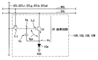
図2は、各画素Pの駆動回路の一構成例を表すブロック図である。駆動基板10上には、サブ画素10R,10G,10B,10Wを含む画素Pが、マトリクス状に複数設けられており、これら複数の画素Pが配設される表示部Sの周辺領域(額縁領域)に、各サブ画素10R,10G,10B,10Wを駆動するための駆動回路30が配設されている。表示部Sでは、複数の走査線WSLおよび電源線DSLが行状に配置され、複数の信号線DTL(後述のDTLr,DTLg,DTLb,DTLwのいずれかに相当)が列状に配置されている。これらの走査線WSL、信号線DTLおよび電源線DSLがそれぞれ、上記駆動回路30に接続されている。尚、駆動回路30は、駆動基板10上に直に設けられていてもよいし、あるいは駆動基板10の周辺領域に接続されたプリント配線基板(FPC)等に集積されたものであってもよい。
(Pixel drive circuit)
FIG. 2 is a block diagram illustrating a configuration example of the drive circuit of each pixel P. A plurality of pixels P including sub-pixels 10R, 10G, 10B, and 10W are provided in a matrix on the driving
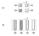
各画素Pにおいて、サブ画素Wは、3原色のサブ画素10R,10G,10Bよりも高輝度を示す(表示装置全体の輝度向上もしくは電力低減を目的として設けられた)サブピクセルである。画素Pでは、これら4色のサブ画素10R,10G,10B,10Wが、例えば図3(A)に示したように、2×2の行列状に設けられていてもよいし、図3(B)に示したように、1方向(行方向または列方向)に沿って配列して設けられていてもよい。このように、4色のサブ画素10R,10G,10B,10Wの配置レイアウトは特に限定されないが、図1の断面図では、説明上、これらの4色のサブ画素10R,10G,10B,10Wを1方向に並列させたものを例示している。
In each pixel P, the sub pixel W is a sub pixel that is higher in luminance than the three primary
駆動回路30は、複数の画素Pを順次選択しつつ、選択された画素P内のサブピクセル10R,10B,10G,10Wに対して映像信号30Aに基づく映像信号電圧を書き込むことにより、複数の画素Pの表示駆動を行うものである。この駆動回路30は、映像信号処理回路31、タイミング生成回路32、走査線駆動回路33、信号線駆動回路34および電源線駆動回路35を有している。
The
映像信号処理回路31は、外部から入力されるデジタルの映像信号30Aに対して所定の映像信号処理(例えば、ガンマ補正処理,オーバードライブ処理等)を行うと共に、そのような映像信号処理後の映像信号31Aを信号線駆動回路34に出力するものである。本実施の形態では、4色のサブ画素を用いて映像表示に行うため、この映像信号処理回路31が、更に所定の変換処理部310を有している。変換処理部310は、例えばR,G,Bの3色に対応する映像信号を、例えばR,G,B,Wの4色に対応する映像信号へ変換する変換処理(RGB/RGBW変換処理)を行うものである。この変換処理部310は、例えば、複数の乗算器および加算器を用いて構成されている。
The video signal processing circuit 31 performs predetermined video signal processing (for example, gamma correction processing, overdrive processing, etc.) on the digital video signal 30A input from the outside, and video after such video signal processing. The
タイミング生成回路32は、外部から入力される同期信号30Bに基づいて制御信号32Aを生成し出力することにより、走査線駆動回路33、信号線駆動回路34および電源線駆動回路35がそれぞれ、連動して動作するように制御するものである。
The timing generation circuit 32 generates and outputs the
走査線駆動回路33は、制御信号32Aに基づいて複数の走査線WSLに対して選択パルスを順次印加することにより、複数の画素P(詳細にはサブ画素10R,10B,10G,10W)を順次選択するものである。信号線駆動回路34は、制御信号32Aに基づいて、映像信号処理回路31から入力される映像信号31Aに対応するアナログの映像信号を生成し、各信号線DTL(詳細には後述のDTLr,DTLg,DTLb,DTLw)に印加するものである。電源線駆動回路35は、制御信号32Aに基づいて複数の電源線DSLに対して制御パルスを順次印加することにより、各画素P内のサブ画素10R,10B,10G,10Wにおける白色有機EL素子10aの発光(点灯)動作および消光(消灯)動作の制御を行うものである。
The scanning
(画素回路)
図4は、サブ画素10R,10G,10B,10Wの回路構成の一例を表したものである。各サブ画素10R,10G,10B,10W内には、白色有機EL素子10aと共に、画素回路36が設けられている。
(Pixel circuit)
FIG. 4 illustrates an example of a circuit configuration of the sub-pixels 10R, 10G, 10B, and 10W. In each of the sub-pixels 10R, 10G, 10B, and 10W, a pixel circuit 36 is provided along with the white
画素回路36は、例えば書き込み(サンプリング用)トランジスタTr1、駆動トランジスタTr2および保持容量素子Csを含んで構成されている。書き込みトランジスタTr1は、ゲートが走査線WSL、ドレインが信号線DTL(DTLr,DTLg,DTLb,DTLw)にそれぞれ接続され、ソースは、駆動トランジスタTr2のゲートおよび保持容量素子Csの一端に接続されている。駆動トランジスタTr2のドレインは電源線DSLに接続され、ソースは、保持容量素子Csの他端および白色有機EL素子10aのアノードに接続されている。白色有機EL素子10aのカソードは、固定電位VSS(例えば、接地電位)に設定されている。書き込みトランジスタTr1および駆動トランジスタTr2はそれぞれ、例えば、nチャネルMOS(Metal Oxide Semiconductor)型のTFT(Thin Film Transistor;薄膜トランジスタ)である。
The pixel circuit 36 includes, for example, a writing (sampling) transistor Tr1, a driving transistor Tr2, and a storage capacitor element Cs. The writing transistor Tr1 has a gate connected to the scanning line WSL, a drain connected to the signal line DTL (DTLr, DTLg, DTLb, DTLw), and a source connected to the gate of the driving transistor Tr2 and one end of the storage capacitor element Cs. . The drain of the drive transistor Tr2 is connected to the power supply line DSL, and the source is connected to the other end of the storage capacitor element Cs and the anode of the white
尚、図4には、4つのサブ画素10R,10G,10B,10Wを纏めて示しているが、サブ画素10R,10G,10B,10Wには、走査線WSLおよび電源線DSLがそれぞれ各サブ画素に共通して接続されている。一方、信号線DTLについては、サブ画素10R,10G,10B,10Wのそれぞれに個別に接続されている(信号線DTLr,DTLg,DTLb,DTLw)。 In FIG. 4, four sub-pixels 10R, 10G, 10B, and 10W are collectively shown. However, the sub-pixels 10R, 10G, 10B, and 10W include a scanning line WSL and a power supply line DSL, respectively. Connected in common. On the other hand, the signal line DTL is individually connected to each of the sub-pixels 10R, 10G, 10B, and 10W (signal lines DTLr, DTLg, DTLb, and DTLw).
(有機EL素子の構成)
白色有機EL素子10aは、駆動基板10上において、例えば第1電極11と第2電極14との間に発光層を含む有機層13を有するものである。具体的には、白色有機EL素子10aでは、サブ画素10R,10G,10B,10W毎に駆動基板10上に第1電極11が設けられており、駆動基板10および第1電極11は、各第1電極11に対向して開口を有する画素間絶縁膜12によって覆われている。画素間絶縁膜12の開口において、第1電極11上に有機層13が形成されており、この有機層13上に、第2電極14が表示領域の全域にわたって設けられている。
(Configuration of organic EL element)
The white
第1電極11は、例えば陽極として機能すると共に、例えば光反射性に優れた導電性材料を用いて構成される。この第1電極11は、例えば、クロム(Cr),金(Au),白金(Pt),ニッケル(Ni),銅(Cu),タングステン(W),アルミニウム(Al)あるいは銀(Ag)等の金属元素の単体または合金よりなる。あるいは、第1電極11は、それらの金属元素の単体または合金よりなる金属膜(ミラーとして機能する部分)と、ITO、InZnO、酸化亜鉛(ZnO)とアルミニウム(Al)との合金等の透明導電膜との積層構造を有していてもよい。本実施の形態では、封止基板20の上方から光取り出しがなされるトップエミッション方式において、第1電極11の一部または全部がミラーとして機能し、白色有機EL素子10aから発せられた光が上方へ向けて反射されるようになっている。第1電極11の膜厚は、所望の反射率(例えば80%〜90%の反射率)が得られるように設定されることが望ましい。
The
画素間絶縁膜12は、各サブ画素10R,10G,10B,10Wの発光領域を電気的に分離し、画素間リークを抑制する機能を有するものである。この画素間絶縁膜12は、例えばポリイミド,アクリル系樹脂またはノボラック系樹脂などの有機絶縁膜により構成されている。
The inter-pixel
有機層13は、有機電界発光層(ここでは、白色発光層)を含んでおり、電界をかけることにより電子と正孔との再結合を生じて、白色光(白色と見做せる疑似白色光も含む)を発生するようになっている。このような白色発光層は、例えば赤色光を発する赤色発光層、緑色光を発する緑色発光層および青色光を発する青色発光層を厚み方向に積層した構造を有している。赤色発光層は、例えば赤色発光材料,正孔輸送性材料および電子輸送性材料のうち少なくとも1種を含み、例えば4,4−ビス(2,2−ジフェニルビニン)ビフェニル(DPVBi)に2,6−ビス[(4'−メトキシジフェニルアミノ)スチリル]−1,5−ジシアノナフタレン(BSN)を混合したものから構成されている。緑色発光層は、例えば、緑色発光材料,正孔輸送性材料および電子輸送性材料のうち少なくとも1種を含み、例えば、ADNやDPVBiにクマリン6を混合したものから構成されている。青色発光層は、例えば、青色発光材料,正孔輸送性材料および電子輸送性材料のうち少なくとも1種を含み、例えば、DPVBiに4,4'−ビス[2−{4−(N,N−ジフェニルアミノ)フェニル}ビニル]ビフェニル(DPAVBi)を混合したものから構成されている。
The
このような有機層13は、また、上記のような発光層の他にも、例えば正孔注入層、正孔輸送層、電子輸送層などを含んでいてもよい。具体的には、第1電極11が陽極として機能する場合には、この第1電極11側から順に、正孔注入層、正孔輸送層、白色発光層および電子輸送層を積層した構造であってもよい。また、白色発光層または電子輸送層と、第2電極14との間には、更に、例えばLiFよりなる電子注入層が設けられていてもよい。また、上記白色発光層と、正孔注入層、正孔輸送層、電子輸送層および電子注入層とは、サブ画素10R,10G,10B,10Wに共通して形成されていてもよいし、サブ画素10R,10G,10B,10W毎に設けられていてもよい。また、それらの層のうちの一部がサブ画素毎に設けられ、その他の層が全サブ画素に共通して設けられていてもよい。
Such an
尚、ここでは、白色発光層として、赤色発光層、緑色発光層および青色発光層を積層したものを例示したが、白色発光層の構成はこれに限定されず、混色により白色光を生成可能な構造であればよい。例えば、青色発光層と黄色発光層とを積層した構造、または青色発光層と橙色発光層とを積層した構造であってもよい。 In this example, the white light emitting layer is a laminate of a red light emitting layer, a green light emitting layer, and a blue light emitting layer. However, the configuration of the white light emitting layer is not limited to this, and white light can be generated by color mixing. Any structure can be used. For example, a structure in which a blue light emitting layer and a yellow light emitting layer are stacked, or a structure in which a blue light emitting layer and an orange light emitting layer are stacked may be employed.
第2電極14は、例えば陰極として機能し、例えばサブ画素10R,10G,10B,10Wに共通して設けられるものである。この第2電極14は、例えばアルミニウム(Al),マグネシウム(Mg),カルシウム(Ca),銀(Ag)およびITO,InZnO,ZnO等の透明導電膜等のうちの少なくとも1種よりなる単体金属、それらのうちの2種以上を含む合金、もしくは金属酸化物から構成されている。第2電極14は、そのような単体金属および合金のうちのいずれかよりなる単層膜であってもよいし、それらのうちの2種以上を積層した積層膜であってもよい。この第2電極14は、第1電極11と絶縁された状態で設けられると共に、保護膜15によって覆われている。
The
保護層15は、絶縁性材料または導電性材料のいずれにより構成されていてもよい。絶縁性材料としては、無機アモルファス性の絶縁性材料、例えばアモルファスシリコン(a−Si),アモルファス炭化シリコン(a−SiC),アモルファス窒化シリコン(a−Si1-xNx)、アモルファスカーボン(a−C)等が好ましい。このような無機アモルファス性の絶縁性材料は、グレインを構成しないため透水性が低く、良好な保護膜となる。この保護層15上に、図示しない接着層を介して封止基板20が貼り合わせられている。
The
封止基板20は、各白色有機EL素子10aを封止するものである。本実施の形態では、上述のようにトップエミッション方式を用いているため、この封止基板20が、サブ画素10R,10G,10B,10Wで発生した各色光に対して透明なガラスなどの材料により構成されている。この封止基板20には、カラーフィルタ層16が設けられている。
The sealing
(カラーフィルタ層16)
カラーフィルタ層16は、各サブ画素10R,10G,10B,10Wに対向して開口(開口M1,Mw)を有するブラックマトリクス16Mを有する。詳細には、カラーフィルタ層16において、ブラックマトリクス16Mは、サブ画素10R,10G,10Bに対向して開口M1を有し、サブ画素10Wに対向して開口Mwを有している。このブラックマトリクス16Mは、例えば黒色の顔料または染料を混入した樹脂よりなる。あるいは、ブラックマトリクス16Mは、例えば、金属,金属窒化物あるいは金属酸化物よりなる薄膜を1層以上積層した薄膜フィルタにより構成されていてもよい。
(Color filter layer 16)
The
ブラックマトリクス16Mの開口M1,Mwのうち、サブ画素10R,10G,10Bに対向する開口M1にのみ、カラーフィルタ(赤色フィルタ16R,緑色フィルタ16Gまたは青色フィルタ16B)が形成されている。即ち、サブ画素10R,10G,10Bにはそれぞれ、対応する色のカラーフィルタ(赤色フィルタ16R,緑色フィルタ16Gまたは青色フィルタ16B)が設けられる一方、サブ画素10Wには、カラーフィルタが設けられていない。
Of the openings M1 and Mw of the
赤色フィルタ16Rは、白色光のうち赤色光を選択的に透過させる(例えば波長620nm〜750nmの範囲に透過帯域を有する)ものである。緑色フィルタ16Gは、白色光のうち緑色光を選択的に透過させる(例えば波長495nm〜570nmの範囲に透過帯域を有する)ものである。青色フィルタ16Bは、白色光のうち青色光を選択的に透過させる(例えば波長450nm〜495nmの範囲に透過帯域を有する)ものである。これらの赤色フィルタ16R,緑色フィルタ16Gまたは青色フィルタ16Bはそれぞれ、例えば顔料または染料を混入した樹脂よりなる。尚、このようなカラーフィルタ層16の表面が有機絶縁材料よりなるオーバーコート膜により覆われていてもよい。
The
このような構成により、白色有機EL素子10a側からの白色光は、サブ画素10R,10G,10Bでは、それぞれR,G,Bの各色光に変換されて表示光として取り出される一方、サブ画素10Wでは、白色光がそのまま(色変換されることなく)開口Mwを通過して表示光として取り出される。本実施の形態では、このようなカラーフィルタ層16のブラックマトリクス16Mにおける開口M1,Mwの開口幅が所定の大小関係となるように設計されている。
With such a configuration, the white light from the white
(ブラックマトリクスの開口設計)
図5(A)は、サブ画素10B、図5(B)はサブ画素10Wの詳細な断面構成を表したものである。図6および図7は、開口の形状およびレイアウトの一例を模式的に表したものである。
(Black matrix opening design)
FIG. 5A shows a detailed cross-sectional configuration of the sub-pixel 10B, and FIG. 5B shows a detailed cross-sectional configuration of the sub-pixel 10W. 6 and 7 schematically show examples of the shape and layout of the openings.
本実施の形態では、サブ画素10Wに対向する開口Mwの幅(開口幅LBM(W))が、サブ画素10R,10G,10Bに対向する開口M1の幅(開口幅LBM)よりも小さくなるように設計されている。具体的には、サブ画素10R,10G,10B(以下、サブ画素10Bを例にして説明する)では、図5(A)に示したように、白色有機EL素子10a上に、開口M1が設けられ、この開口M1に青色フィルタ16Bが形成されている。ここで、開口M1は、一般に、画素開口(第1電極11に対応する部分)よりも大きくなるように設けられる。これは、以下のような理由による。
In the present embodiment, the width of the opening Mw facing the sub-pixel 10W (opening width L BM (W)) is smaller than the width of the opening M1 facing the sub-pixels 10R, 10G, 10B (opening width L BM ). Designed to be Specifically, in the sub-pixels 10R, 10G, and 10B (hereinafter described by taking the sub-pixel 10B as an example), as illustrated in FIG. 5A, an opening M1 is provided on the white
即ち、トップエミッション方式の有機EL表示装置1では、封止基板20側にブラックマトリクス16Mを含むカラーフィルタ層16が設けられる。このような構成において、駆動基板10との貼り合せ時のアライメント精度を保持する(位置ずれの影響を吸収するマージンを確保する)と共に、表示面(ここでは、封止基板20の上面)を斜め方向から見た場合の遮光(いわゆるケラレ)を抑制して、各サブ画素での視野角特性を向上させるためである。ここで、ある観察方向(基板法線方向から角度θ1(0°≦θ1<90°)傾いた斜め方向)における遮光率Zは、例えば以下の式(1)と式(2)によって決まる。つまり、R,G,Bの3色に対応するサブ画素10R,10G,10Bでは、ブラックマトリクス16Mにおいて、遮光率Zが最小限となるように開口幅LBMが設計されている。詳細には、隣接画素からの色光のクロストークや、外光反射等を抑制できる程度の遮光性能を保持しつつ、ケラレの影響を抑えることができる遮光率Zとなるような設計がなされている。
That is, in the top emission type organic
Lshadow=Σi[ti・tan{sin-1(nair・sinθair/nsub(i))]] ………(1)
Z=(LP+d−Lshadow)/LP ………(2)
但し、
Lshadow:遮光幅
ti:第1電極11の金属反射面とブラックマトリクス16Mとの間に積層された各層の厚み
nsub(i):第1電極11の金属反射面とブラックマトリクス16Mとの間に積層された各層の屈折率
nair:大気の屈折率
LP:第1電極11の幅(画素幅)
d:開口幅LBMと画素幅LPとの差(開口マージン)
L shadow = Σ i [t i · tan {sin −1 (n air · sin θ air / n sub (i) )]] (1)
Z = (L P + d−L shadow ) / L P (2)
However,
L shadow : light shielding width t i : thickness of each layer laminated between the metal reflecting surface of the
d: Difference between the opening width L BM and the pixel width L P (opening margin)
一方、斜め方向におけるカラーフィルタ透過率Tは、スネルの法則およびランバートベールの法則により、式(A),(B)のように表される。尚、式(A)における記号「^」は「べき乗」を表し、例えば「B^2」は「B2」を意味する。つまり、カラーフィルタの透過率が異なる場合、観測角度θ1が大きくなるほど透過率の差異が大きくなり、斜め方向における色度変化が生じる。
T=T0^(1/cosθ2) ………(A)
sinθ1/sinθ2=nCF ………(B)
但し、
T0:カラーフィルタ(16R,16G,16B)の正面での透過率
θ2:カラーフィルタ(16R,16G,16B)中の光線透過角度
θ1:観察角度(視野角)
nCF:観察環境とカラーフィルタ(16R,16G,16B)との屈折率比
を示す。
On the other hand, the color filter transmittance T in the oblique direction is expressed as in equations (A) and (B) by Snell's law and Lambert-Beer's law. Note that the symbol “^” in the formula (A) represents “power”, and for example, “B ^ 2” means “B 2 ”. That is, when the transmittances of the color filters are different, the difference in transmittance increases as the observation angle θ 1 increases, and chromaticity changes in an oblique direction.
T = T 0 ^ (1 / cosθ 2 ) (A)
sinθ 1 / sinθ 2 = n CF (B)
However,
T 0 : transmittance in front of the color filters (16R, 16G, 16B) θ 2 : light transmission angle in the color filters (16R, 16G, 16B) θ 1 : observation angle (viewing angle)
n CF : Indicates the refractive index ratio between the observation environment and the color filters (16R, 16G, 16B).
一方、図5(B)に示したように、サブ画素10Wでは、他のサブ画素(ここでは、サブ画素10B)と同様、白色有機EL素子10a上に開口Mwが設けられ、この開口Mwについても、上記と同様の理由から、画素幅LPよりも大きくなるように設けられる。但し、サブ画素10Wに対向する開口Mwの開口幅LBM(W)は、上記開口幅LBMよりも小さくなっている。
On the other hand, as shown in FIG. 5B, in the sub-pixel 10W, an opening Mw is provided on the white
このように、本実施の形態では、サブ画素10Wにおいて、開口幅LBM(W)が他のサブ画素の開口幅LBMよりも小さく設定されることにより、遮光率Zが大きくなり、透過率が低減されている。但し、この際、サブ画素10R,10G,10Bにおける、赤色フィルタ16R,緑色フィルタ16G,青色フィルタ16Bの各透過率Tを考慮して(サブ画素10Wにおける透過率が、各カラーフィルタの透過率Tと同等となるように)、開口幅LBM(W)が設定されることが望ましい。尚、上記式(A)における透過率T0は、カラーフィルタ材料の濃度および厚み等に応じて変化するものであり、各サブ画素10R,10G,10B毎に異なるものである。
As described above, in the present embodiment, in the sub-pixel 10W, the opening width L BM (W) is set smaller than the opening width L BM of the other sub-pixels, so that the light shielding ratio Z is increased and the transmittance is increased. Has been reduced. However, at this time, the transmittances T of the
ここでは、4色のサブ画素10R,10G,10B,10Wの各画素幅LPは互いに同一であることから、サブ画素10Wにおける開口マージンdWが、サブ画素10Bの開口マージンdよりも小さく(狭く)設計されている。これにより、サブ画素10Wでは、上述の式(1),(2)によって定められる遮光率Zが、サブ画素10Bのそれよりも大きくなり、この傾向は、詳細は後述するが、特に観察角度θ1が大きくなるほど増す。
Here, four-
実際には、画素の形状(第1電極11の面形状)は、図6および図7に示したように、例えば方形(矩形または正方形)となっている。このように、サブ画素10R,10G,10Bにおいて、X方向およびY方向の各方向に沿って開口マージンdを有する場合、サブ画素10Wにおいても、X方向およびY方向の各方向に沿って、開口マージンdWを設けるとよい。具体的には、サブ画素10R,10G,10Bでは、X方向において、画素幅LP1に対して開口マージンdを考慮した開口幅LBM1、Y方向において、画素幅LP2に対して開口マージンdを考慮した開口幅LBM2にそれぞれ設計される。一方、サブ画素10Wでは、X方向において、画素幅LP1に対して開口マージンdwを考慮した開口幅LBM(W)1、Y方向において、画素幅LP2に対して開口マージンdwを考慮した開口幅LBM(W)2にそれぞれ設計される。尚、X方向およびY方向は、表示面(基板面)に平行な面内において互いに直交する2方向とする。
Actually, the shape of the pixel (the surface shape of the first electrode 11) is, for example, a square (rectangular or square) as shown in FIGS. As described above, when the
尚、ここでは、R,G,Bの3色に対応するサブ画素10R,10G,10Bについては、互いに同一の開口幅LBMおよび開口マージンdとなるように設定したが、これらの開口幅LBMおよび開口マージンdは、各サブ画素間において必ずしも同一でなくともよい。赤色フィルタ16R,緑色フィルタ16Gおよび青色フィルタ16Bの間でも、透過帯域が互いに異なると共に、顔料の濃度等の他の設計条件に依存して、サブ画素間で透過率(特に斜め方向における透過率)に差が生じる場合もある。このため、そのような透過率差を軽減するために、サブ画素10R,10G,10Bのいずれかにおいて他のサブ画素よりも開口幅が小さく(または大きく)なるように、あるいはサブ画素10R,10G,10B,10Wにおける各開口幅が互いに異なるように(透過波長毎に)、設計されていてもよい。例えば、RGBの各透過波長帯域における透過率を、各カラーフィルタの濃度に相関させて(各カラーフィルタ濃度を考慮して)調整したものが挙げられる。これにより、サブ画素10R,10G,10B間において各透過率に差がある場合にも、それを低減して、より所望の色度を得易くなる。
Here, the sub-pixels 10R, 10G, and 10B corresponding to the three colors R, G, and B are set to have the same opening width L BM and opening margin d, but these opening widths L The BM and the opening margin d are not necessarily the same between the sub-pixels. Even among the
また、X方向とY方向との各方向において、開口マージンd,dwを同一幅としたが、各方向において異なるようにしてもよい。例えば、X,Y方向のうちの選択的な一方向(例えば水平方向に一致する方向)における開口幅のみを調整し、もう一方の方向(例えば垂直方向に一致する方向)では4つのサブ画素間で同一の開口幅となるようにしてもよい。あるいは、X方向とY方向とにおいて、開口幅の調整比率が異なっていてもよい。これにより、特に良好な視野角特性(色度)が必要となる方向においてのみ選択的に開口制御(透過率制御)を行うことができ、他の方向では、サブ画素10Wの開口幅を小さくすることなく反射率抑制の効果を得られるようにすることができる。 In addition, the opening margins d and dw have the same width in each of the X direction and the Y direction, but they may be different in each direction. For example, only the aperture width in one of the X and Y directions (for example, the direction that matches the horizontal direction) is adjusted, and in the other direction (for example, the direction that matches the vertical direction), between the four sub-pixels. The opening width may be the same. Alternatively, the opening width adjustment ratio may be different between the X direction and the Y direction. Thereby, aperture control (transmittance control) can be selectively performed only in a direction where particularly good viewing angle characteristics (chromaticity) are required, and the aperture width of the sub-pixel 10W is reduced in other directions. Thus, the effect of suppressing the reflectance can be obtained.
[作用・効果]
有機EL表示装置1では、図2および図4に示したように、駆動回路30が、映像信号30Aおよび同期信号30Bに基づき、表示部S内の各画素Pを駆動し、4色のサブ画素10R,10B,10G,10Wを用いて表示駆動を行う。この際、映像信号処理回路30は、各サブピクセル10R,10B,10G,10Wへ供給する映像信号を生成するために、R,G,Bの3色に対応する映像信号30Aに対し、以下に説明するような変換処理を施す。
[Action / Effect]
In the organic
(R,G,B,Wの映像信号への変換処理)
ここで一般に、入力される映像信号30Aは、R,G,Bの3色に対応するものであるため、映像信号処理回路31は、まず、入力された映像信号30A(R,G,Bの3色に対応する映像信号)に対して、以下のような変換処理(RGB/RGBW変換処理)を行う。図8に、この変換処理部310における処理フローを示す。
(Conversion processing to R, G, B, W video signals)
Here, generally, since the input video signal 30A corresponds to three colors of R, G, and B, the video signal processing circuit 31 first receives the input video signal 30A (R, G, B). The following conversion processing (RGB / RGBW conversion processing) is performed on the video signals corresponding to the three colors). FIG. 8 shows a processing flow in the
即ち、変換処理部310は、まず、R,G,Bの3色に対応する映像信号(入力映像信号(R,G,B))を取得する(ステップS101)。次いで、変換処理部310は、この入力映像信号(R,G,B)を、CIE(Commission Internationale de l'Eclairage)により規定される表色系である3刺激値に対応する映像信号(X,Y,Z)に変換する(ステップS102)。
That is, the
具体的には、パネル固有のR,G,Bの飽和色を予め測定しておき、その測定結果に基づき、例えば以下の式(3)により規定される変換マトリクス(変換行列)Mを求める。次いで、この変換マトリクスMの逆行列M-1を用いて、以下の式(4)に基づき、色域を決定する画素(サブ画素10R,10G,10B)を用いた場合の所望の白色点(白色点Aとする)における混合比率(r,g,b)を求める。このようにして求めた混合比率(r,g,b)を用い、以下の式(5),(6)に基づき、入力映像信号(R,G,B)を、映像信号(X,Y,Z)に変換する。 Specifically, the saturation colors of R, G, and B specific to the panel are measured in advance, and a conversion matrix (conversion matrix) M defined by, for example, the following equation (3) is obtained based on the measurement result. Next, using the inverse matrix M −1 of the conversion matrix M, a desired white point (when the pixels (subpixels 10R, 10G, 10B) for determining the color gamut are used based on the following equation (4) ( The mixing ratio (r, g, b) at white point A) is obtained. Using the mixing ratio (r, g, b) thus obtained, the input video signal (R, G, B) is converted into the video signal (X, Y, B) based on the following equations (5), (6). Z).

尚、上記式中のRx,Gx,Bx,Wxは、サブ画素10R,10G,10B,10Wの飽和色を示す色度のx座標に対応する値であり、Ry,Gy,By,Wyは、サブ画素10R,10G,10B,10Wの飽和色を示す色度のy座標に対応する値であり、Rz,Gz,Bz,Wzは、サブ画素10R,10G,10B,10Wの飽和色を示す色度のz座標(即ち、1−x−y)に対応する値を示す。 Note that Rx, Gx, Bx, and Wx in the above formula are values corresponding to the x coordinate of the chromaticity indicating the saturated color of the sub-pixels 10R, 10G, 10B, and 10W, and Ry, Gy, By, and Wy are It is a value corresponding to the y coordinate of the chromaticity indicating the saturated color of the sub-pixels 10R, 10G, 10B, and 10W, and Rz, Gz, Bz, and Wz are colors indicating the saturated colors of the sub-pixels 10R, 10G, 10B, and 10W. A value corresponding to the z coordinate of degrees (ie, 1-xy) is shown.
また、入力映像信号(R,G,B)は、例えば各色について8ビットまたは16ビットの映像信号であり、例えば2.2乗等のガンマ関数に従ってその強度を表したものであるが、各サブ画素の発光色度点および輝度を規定するものであれば、これには限られない。更に、入力映像信号(R,G,B)から映像信号(X,Y,Z)への変換手法については、上記した手法には限られず、他の公知の手法を用いてもよい。加えて、上記白色点Aは1つに限らず、複数点設定することができ、それら複数の白色点Aに対する変換マトリクスMを求めておいてもよい。また、変換マトリクスMは、パネル内の表示部S全域の画素Pを対象として求めてもよいし、画素Pあるいは選択的な領域(複数の画素Pを含む)を対象としてもよい。 The input video signal (R, G, B) is an 8-bit or 16-bit video signal for each color, for example, and represents its intensity according to a gamma function such as a power of 2.2. The present invention is not limited to this as long as it defines the emission chromaticity point and luminance of the pixel. Furthermore, the conversion method from the input video signal (R, G, B) to the video signal (X, Y, Z) is not limited to the above-described method, and other known methods may be used. In addition, the number of the white points A is not limited to one, and a plurality of points can be set, and a conversion matrix M for the plurality of white points A may be obtained. The conversion matrix M may be obtained for the pixels P in the entire display unit S in the panel, or may be the pixels P or selective areas (including a plurality of pixels P).
次に、変換処理部310は、3刺激値に対応する映像信号(X,Y,Z)によって表現される色度を、サブ画素10Wを含めたR,G,B,Wの4色のサブ画素10R,10G,10B,10Wにより表現し得る映像信号(変換映像信号(r,g,b,w))を生成する。
Next, the
具体的には、まず、上記R,G,Bに加えて、Wについてのパネル固有の飽和色を予め測定しておき、その測定結果に基づいて、以下の式(7)〜(9)により規定される変換マトリクスMr,Mg,Mbを求める。尚、これらの変換マトリクスMr,Mg,Mbは、R,G,B,Wの各飽和色のうち、(W,G,B)、(R,W,B)および(R,G,W)の各組み合わせによって得られるものである。 Specifically, first, in addition to the above R, G, and B, a panel-specific saturated color for W is measured in advance, and based on the measurement results, the following equations (7) to (9) are used. A prescribed conversion matrix Mr, Mg, Mb is obtained. These conversion matrices Mr, Mg, and Mb are (W, G, B), (R, W, B), and (R, G, W) among the saturated colors of R, G, B, and W. It is obtained by each combination.
次いで、この変換マトリクスMr,Mg,Mbの逆行列Mr-1,Mg-1,Mb-1と、映像信号(X,Y,Z)を用いて、以下の式(10)〜(15)に基づき、(Wp,Gp,Bp)、(Rp,Wp,Bp)および(Rp,Gp,Wp)の各組み合わせのうち、いずれの値も0(ゼロ)以上になる組み合わせを求める。そして、この組み合わせに含まれない色の映像信号(R,G,Bのいずれか)を0として、R,G,B,Wの4色に対応する変換映像信号(r,g,b,w)を生成する。 Next, using the inverse matrix Mr −1 , Mg −1 , Mb −1 of the conversion matrix Mr, Mg, Mb and the video signal (X, Y, Z), the following equations (10) to (15) are obtained. Based on the combinations of (Wp, Gp, Bp), (Rp, Wp, Bp), and (Rp, Gp, Wp), a combination in which all values are 0 (zero) or more is obtained. Then, the video signal (any one of R, G, B) not included in this combination is set to 0, and the converted video signal (r, g, b, w) corresponding to the four colors R, G, B, W is set. ) Is generated.
例えば、まず、式(10),(13)〜(15)に基づいて、(Wp,Gp,Bp)を求め、これらのWp,Gp,Bpの各値が0以上であるか否かを判定し、Wp,Gp,Bpのいずれの値も0以上となる場合には(ステップS103:Y)、Rの映像信号を0と置き換えた映像信号(0,Gp,Bp,Wp)を、変換映像信号(r,g,b,w)とする(ステップS104)。 For example, first, (Wp, Gp, Bp) is obtained based on the equations (10), (13) to (15), and it is determined whether or not each value of these Wp, Gp, Bp is 0 or more. If all the values of Wp, Gp, and Bp are equal to or greater than 0 (step S103: Y), a video signal (0, Gp, Bp, Wp) in which the R video signal is replaced with 0 is converted into a converted video. Signals (r, g, b, w) are set (step S104).
一方、Wp,Gp,Bpの各値のいずれかが0未満である場合には(ステップS103:N)、式(11),(13)〜(15)に基づいて、(Rp,Wp,Bp)を求め、これらのRp,Wp,Bpの各値が0以上であるか否かを判定する(ステップS105)。この結果、Rp,Wp,Bpのいずれの値も0以上である場合には(ステップS105:Y)、Gの映像信号を0と置き換えた映像信号(Rp,0,Bp,Wp)を、変換映像信号(r,g,b,w)とする(ステップS106)。一方、Rp,Wp,Bpの各値のいずれかが0未満の場合には(ステップS105:N)、式(12),(13)〜(15)に基づいて、(Rp,Gp,Wp)を求め、Bの映像信号を0と置き換えた映像信号(Rp,Gp,0,Wp)を変換映像信号(r,g,b,w)とする(ステップS107)。 On the other hand, if any of the values of Wp, Gp, Bp is less than 0 (step S103: N), (Rp, Wp, Bp) based on the equations (11), (13) to (15) ) And determine whether or not each of these values of Rp, Wp, and Bp is 0 or more (step S105). As a result, when all the values of Rp, Wp, and Bp are 0 or more (step S105: Y), the video signal (Rp, 0, Bp, Wp) in which the G video signal is replaced with 0 is converted. The video signal (r, g, b, w) is set (step S106). On the other hand, if any of the values of Rp, Wp, Bp is less than 0 (step S105: N), (Rp, Gp, Wp) based on the equations (12), (13) to (15) The video signal (Rp, Gp, 0, Wp) in which the B video signal is replaced with 0 is set as the converted video signal (r, g, b, w) (step S107).
次いで、上記のようにして生成した変換映像信号(r,g,b,w)を、例えば所定のルックアップテーブル(LUT)を用いて、所望の値(発光強度)に変換する(ステップS108)。このようにして、各サブ画素10R,10G,10B,10Wへの供給用の映像信号(出力映像信号(R,G,B,W))を生成し、出力する(ステップS109)。但し、このような発光強度の変換は、LUTを用いて行うのではなく、ガンマカーブや近似式を用いた演算によって行うようにしてもよい。また、このステップS108の変換処理を行わないようにしてもよい。以上により、変換処理部310における変換処理が終了となる。
Next, the converted video signal (r, g, b, w) generated as described above is converted into a desired value (light emission intensity) using, for example, a predetermined lookup table (LUT) (step S108). . In this way, the video signals (output video signals (R, G, B, W)) to be supplied to the sub-pixels 10R, 10G, 10B, 10W are generated and output (step S109). However, such conversion of the light emission intensity may be performed not by using the LUT but by calculation using a gamma curve or an approximate expression. Further, the conversion process in step S108 may not be performed. Thus, the conversion process in the
(発光駆動動作)
次に、上記のような映像信号に基づく発光駆動動作について説明する。即ち、上記変換処理によって生成された4色のいずれかに対応する映像信号電圧が信号線DTLに印加され、かつ電源線DSLに所定の電圧が印加されている期間中に、走査線駆動回路33が、走査線WSLの電圧をオフ電圧からオン電圧へ上げる。これにより、書き込みトランジスタTr1がオン状態となり、駆動トランジスタTr2のゲート電位Vgが映像信号電圧へと上昇する。その結果、補助容量素子Csに対して映像信号電圧が書き込まれ、保持される。尚、この段階では、まだ、白色有機EL素子10aのアノード−カソード間には電流が流れない(白色有機EL素子10aが発光しない)。駆動トランジスタTr2から供給される電流Idは、白色有機EL素子10aのアノード−カソード間に並列に存在する素子容量(図示せず)へと流れ、この素子容量が充電される。
(Light emission drive operation)
Next, the light emission driving operation based on the video signal as described above will be described. That is, the scanning
続いて、走査線駆動回路33が、走査線WSLの電圧をオン電圧からオフ電圧へと下げると、書き込みトランジスタTr1がオフ状態となり、駆動トランジスタTr2のゲートがフローティングとなる。これにより、駆動トランジスタTr2のドレイン−ソース間に電流Idが流れ、ソース電位Vsおよびゲート電位Vgが上昇する。これにより、白色有機EL素子10aでは、アノード電圧が上昇し、アノード−カソード間に、補助容量素子Csに保持された映像信号電圧(ゲート−ソース間電圧Vgs)に応じた駆動電流(電流Id)が流れる。
Subsequently, when the scanning
この結果、各サブ画素10R,10B,10G,10W内の白色有機EL素子10aへ駆動電流が注入され、有機層13内の発光層(白色発光層)において正孔と電子とが再結合し、白色光が生じる。この白色光のうち上方(封止基板20側)へ発せられた光は、そのままカラーフィルタ層16へ向かい、下方(駆動基板10側)へ発せられた光は、第1電極11において上方へ反射された後、カラーフィルタ層16へ向かう。これにより、サブ画素110R,10B,10G,10Wのそれぞれにおいて、白色光がカラーフィルタ層16へ入射する。
As a result, drive current is injected into the white
ここで、カラーフィルタ層16では、ブラックマトリクス16Mに、サブ画素110R,10B,10Gに対向して開口M1および対応色のフィルタ(赤色フィルタ16R,緑色フィルタ16G,青色フィルタ16B)を有し、サブ画素10Wに対向して開口Mw(カラーフィルタなし)を有している。このため、サブ画素10R,10G,10Bでは、白色有機EL素子10a側からの白色光が、赤色フィルタ16R,緑色フィルタ16Gまたは青色フィルタ16Bをそれぞれ通過して、赤,緑,青の各色光が表示光として上面側(封止基板20側)から取り出される。一方、サブ画素10Wでは、上記白色光が、そのまま表示光として上面側から取り出される。このようにして、有機EL表示装置1では、フルカラーの映像表示がなされる。また、4色のサブ画素10R,10G,10B,10Wを用いて上記のように映像表示を行うことにより、R,G,Bの3色のサブ画素のみを用いる場合と比べ、輝度効率が向上し、低消費電力化が図られる。
Here, the
(ブラックマトリクス開口形状による作用)
上述のように、白色有機EL素子10a側からの白色光は、サブ画素10R,10G,10Bでは、対応するカラーフィルタ(16R,16G,16B)を透過して、それぞれR,G,Bの表示光として取り出される一方、サブ画素10Wでは、白色光がそのまま表示光として取り出される。
(Effects of the black matrix opening shape)
As described above, white light from the white
そのため、白色有機EL素子10aからの白色光のうち、サブ画素10R,10G,10Bでは、カラーフィルタ(16R,16G,16B)により特定の帯域の色光のみが選択的に取り出されることになり、カラーフィルタを有さない高輝度を示すサブ画素10Wに比べ表示光の透過率(輝度)が低くなる。即ち、R,G,Bのサブ画素10R,10G,10Bと、Wのサブ画素10Wとの間で透過率に差が生じる。具体的には、サブ画素10R,10G,10Bでは、透過率が約75〜85%程度となり、サブ画素10Wでは、100%に近くなる。このような透過率差が生じると、各色間での輝度バランスが崩れ、所望の色度を表現しにくくなる。
For this reason, among the white light from the white
また、ブラックマトリクス16Mの開口M1に形成されるカラーフィルタ(16R,16G,16B)では、光の透過方向(フィルタ内を通過する光の進行方向)によって、光路長が異なる。このため、光路長がより長くなる斜め方向(正面方向(基板法線方向)から傾いた方向)では、正面方向に比べ、透過光量が減少し易い。従って、サブ画素10R,10G,10Bでは、特に斜め方向において透過率が低くなる傾向がある。一方、サブ画素10Wでは、そのようなカラーフィルタが設けられていないために、斜め方向においても透過率はそれほど低下しない。つまり、特に斜め方向において、サブ画素10R,10G,10Bとサブ画素10Wとの間の透過率差が顕著となり、色度点が正面方向の色度点から更にずれたものとなり、視野角特性の低下を招く。
Further, in the color filters (16R, 16G, 16B) formed in the opening M1 of the
他方、上述したように、斜め方向における透過率は、サブ画素10R,10G,10Bでは、上記式(1),(2)で表される遮光率Zと、カラーフィルタ(16R,16G,16B)の材料,濃度等とにより概ね決定され、サブ画素10Wでは、遮光率Zにより概ね決定される。 On the other hand, as described above, in the sub-pixels 10R, 10G, and 10B, the transmittance in the oblique direction is the light shielding ratio Z expressed by the above formulas (1) and (2) and the color filters (16R, 16G, and 16B). The sub-pixel 10W is generally determined by the light shielding rate Z.
ここで、本実施の形態では、図5〜図7に示したように、カラーフィルタ層16に配置されるブラックマトリクス16Mにおいて、サブ画素10Wに対向する開口Mwの開口幅LBM(W)が、サブ画素10R,10G,10Bの開口M1の開口幅LBMよりも小さくなるように設計されている。これにより、図9(A)に示したように、サブ画素10R,10G,10B(ここではサブ画素10Bを例示する)では、斜め方向へ向かって透過(出射)する色光(図中破線矢印)の光量がより多くなるように、上述したような観点から最適な開口幅LBMおよび開口マージンdが設定されている。一方、図9(B)に示したように、サブ画素10Wでは、開口Mwが、そのような開口幅LBMよりも小さな開口幅LBM(W)を有することにより、サブ画素10Bよりも斜め方向へ向かって透過する色光がブラックマトリクスMwによって遮光され易くなる(ケラレが生じ易い)。このように、サブ画素10Bの一部、即ちブラックマトリクス16Mの開口Mwのエッジ付近におけるケラレを利用することにより、サブ画素10Wでは、斜め方向における透過率が軽減される。よって、特に透過率差が顕著となる斜め方向において、サブ画素間での透過率差が軽減され、視野角全体において良好な輝度バランスが保持される。
Here, in the present embodiment, as shown in FIGS. 5 to 7, in the
また、本実施の形態では、開口幅LBM(W)は、開口幅LBMと同様、画素幅Lpよりも大きくなるように設計されているため、正面方向における透過率については低下しない。上述したように、各サブ画素間での透過率差は、斜め方向において顕著にあらわれるため、正面方向よりも斜め方向における透過率差を軽減することにより、各サブ画素間における透過率の近似を効率的に行うことができる。 In the present embodiment, the aperture width L BM (W) is designed to be larger than the pixel width Lp, similarly to the aperture width L BM, and thus the transmittance in the front direction does not decrease. As described above, the transmittance difference between the sub-pixels is conspicuous in the oblique direction. Therefore, the transmittance difference between the sub-pixels is approximated by reducing the transmittance difference in the oblique direction rather than the front direction. Can be done efficiently.
例えば、図10に、帯域透過率0.8を有する青色フィルタ16Bが設けられたサブ画素10Bと、透過率が0.99である(高透過率フィルタを設けた)サブ画素10Wとの視野角に対する透過率変化について示す。具体的には、実施例として、サブ画素10B(画素幅LP:50μm,開口幅LBM:70μm,開口マージンd:10μm)の透過率B1と、サブ画素10W(画素幅LP:50μm,開口幅LBM(W):65μm,開口マージンdw:7.5μm)の透過率W1について示す。また、比較例として、サブ画素10Bと同様の画素幅LP,開口幅LBM,開口マージンdで設計したサブ画素10Wについての透過率W100についても示す。
For example, in FIG. 10, the viewing angle between the sub-pixel 10B provided with the
このように、開口幅および開口マージンを同一とした場合、サブ画素10Bの透過率B1と、サブ画素10Wの透過率W100との間に透過率差が生じ、特に観察角度θ1が大きくなる斜め方向においてその差が大きくなることがわかる。これに対し、開口幅および開口マージンをサブ画素10Bよりも小さくなるように設計したサブ画素10Wの透過率W1は、比較例の透過率W100に比べ、サブ画素10Bの透過率B1に近似することがわかる。 As described above, when the aperture width and the aperture margin are the same, a transmittance difference is generated between the transmittance B1 of the sub-pixel 10B and the transmittance W100 of the sub-pixel 10W, and in particular, an oblique angle that increases the observation angle θ 1. It can be seen that the difference increases in the direction. On the other hand, the transmittance W1 of the sub-pixel 10W designed so that the opening width and the opening margin are smaller than those of the sub-pixel 10B should be approximated to the transmittance B1 of the sub-pixel 10B compared to the transmittance W100 of the comparative example. I understand.
また、一定の発光スペクトル下において、上記実施例に係るサブ画素10B,10Wを、混合させて点灯した場合の視野角に対する色度変化について、図11に示す。また、比較例として、上記のようにそれぞれを同一の開口幅および開口マージンで設計したサブ画素10B,10Wを混色させた場合の色度変化について示す。開口幅および開口マージンをサブ画素10Bよりも小さく設計したサブ画素10Wを用いた実施例では、それらを同一に設計した比較例に比べ、観察角度θ1が増しても、色度変化がほとんどみられなかった。これにより、サブ画素間の透過率差によって生じる色度変化(特に視野角の変化に伴って変化する色度変化)が、サブ画素10Wの開口幅制御によって抑制されることがわかる。
FIG. 11 shows changes in chromaticity with respect to the viewing angle when the sub-pixels 10B and 10W according to the above-described example are mixed and lit under a fixed emission spectrum. Further, as a comparative example, a change in chromaticity when sub-pixels 10B and 10W each designed with the same opening width and opening margin as described above are mixed will be described. In the example using the sub-pixel 10W in which the aperture width and the aperture margin are designed to be smaller than those of the sub-pixel 10B, even if the observation angle θ1 is increased, the chromaticity change is almost seen as compared with the comparative example in which they are designed identically. There wasn't. Thereby, it can be seen that a chromaticity change (particularly a chromaticity change that changes with a change in viewing angle) caused by a difference in transmittance between subpixels is suppressed by the aperture width control of the
以上のように本実施の形態では、各画素Pが、R,G,Bに対応するサブ画素10R,10G,10Bと、これらよりも高輝度を示すサブ画素10Wとを有し、サブ画素10R,10G,10Bにはカラーフィルタ(16R,16G,16B)が設けられている。サブ画素10Wにおいて、白色有機EL素子10aから発せられた白色光の透過率が、その一部または全部において低減するように構成されている。具体的には、本実施の形態では、トップエミッション方式による有機EL表示装置1において、サブ画素10Wでは、ブラックマトリクス16Mの開口幅LBM(W)が、他のサブ画素における各開口幅LBMよりも小さくなっている。これにより、サブ画素10Wの一部において白色光のけられ(ケラレ)が、他のサブ画素よりも多く生じ、特に斜め方向へ出射する光の透過率が低減される。従って、カラーフィルタ(16R,16G,16B)を有するサブ画素10R,10G,10Bとカラーフィルタを有さないサブ画素10Wとの間の透過率差が軽減される。ここで、上記のようなサブ画素間における透過率差は視野角変化に伴って大きくなる傾向を有するが、そのような開口幅制御を行うことにより、特に斜め方向からみた場合に、所望の輝度および色度を表現できる。よって、4色のサブ画素を用いて映像表示を行う際に、高画質化を実現することが可能となる。
As described above, in the present embodiment, each pixel P includes the sub-pixels 10R, 10G, and 10B corresponding to R, G, and B, and the sub-pixel 10W that exhibits higher luminance than these, and the sub-pixel 10R. , 10G, 10B are provided with color filters (16R, 16G, 16B). In the sub-pixel 10W, the transmittance of white light emitted from the white
次に、第2の実施の形態および変形例について説明する。以下では、各形態における概略構成または要部構成のみを示し、また、上記第1の実施の形態と同様の構成要素については同一の符号を付し適宜説明を省略する。 Next, a second embodiment and a modification will be described. In the following, only a schematic configuration or a main configuration in each embodiment is shown, and the same components as those in the first embodiment are denoted by the same reference numerals and description thereof is omitted as appropriate.
<第2の実施の形態>
図12は、本開示における第2の実施の形態に係る表示装置(有機EL表示装置2)の断面構成を表したものである。有機EL表示装置2は、上記第1の実施の形態の有機EL表示装置1と同様、いわゆるトップエミッション方式により、フルカラーの映像表示を行うものである。この有機EL表示装置2は、また、4色のサブ画素10R,10G,10B,10Wを用いて上記映像表示を行うものであり、これらのサブ画素10R,10G,10B,10Wはいずれも、発光素子として白色有機EL素子10aを含んでいる。また、この白色有機EL素子10aは、駆動基板10および封止基板20間に設けられると共に、封止基板20側にカラーフィルタ層16が形成されている。
<Second Embodiment>
FIG. 12 illustrates a cross-sectional configuration of a display device (organic EL display device 2) according to the second embodiment of the present disclosure. Similar to the organic
また、本実施の形態においても、カラーフィルタ層16が、各サブ画素10R,10G,10B,10Wに対向して開口M1を有するブラックマトリクス16Mを有すると共に、サブ画素10R,10G,10Bでは、その開口M1にカラーフィルタ(16R,16G,16B)が形成されている。
Also in the present embodiment, the
但し、本実施の形態では、上記第1の実施の形態と異なり、カラーフィルタ層16において、ブラックマトリクス16Mの開口M1の開口幅LBMおよび開口マージンd(図12には図示せず)が各サブ画素間において互いに同一となっている。また、サブ画素10Wでは、NDフィルタ17(減光フィルタ)が形成されている。このNDフィルタ17は、例えばサブ画素10Wの全域において透過光量を低減させる機能フィルタである。このNDフィルタ17の透過率は、他のサブ画素10R,10G,10Bと同等に設定されていることが望ましい。
However, in the present embodiment, unlike the first embodiment, the
本実施の形態のように、サブ画素10Wに透過率制御機能を有するNDフィルタ17を設けることによっても、ブラックマトリクス16Mの開口幅制御を行う上記第1の実施の形態と同等の効果を得ることができる。
As in the present embodiment, by providing the sub-pixel 10W with the
例えば、図13に、帯域透過率0.8を有する青色フィルタ16Bが設けられたサブ画素10Bの視野角に対する透過率変化(透過率B2)と、全可視波長帯域において概ね0.8の透過率を有するNDフィルタ17を設けたサブ画素10Wの視野角に対する透過率変化(透過率W2)について示す。この際、サブ画素10B,10Wのいずれにおいても、画素幅LPを50μm,開口幅LBMを70μmとした。
For example, FIG. 13 shows a change in transmittance (transmittance B2) with respect to the viewing angle of the sub-pixel 10B provided with the
このように、NDフィルタ17を有するサブ画素10Wを用いた場合、サブ画素10B,10Wの透過率B2,W2は略一致し、視野角変化に伴う透過率の差異はほとんど存在しないことがわかった。尚、ここでは、NDフィルタ17として、サブ画素10Wの全域にわたって透過率を低減するものを例示したが、このNDフィルタ17の透過率はサブ画素10W全域において一律であってもよいし、領域毎に異なっていてもよい。例えば、図14(A)に示したように、中央領域d1よりも端部領域d2において低透過率となるように構成されたNDフィルタ17Aであってもよい。また、図14(B)に示したように、中央領域d1から領域d2,d3,端部領域d4にかけて段階的に透過率が低減するように構成されたNDフィルタ17Bであってもよい。更には、図14(C)に示したように、中央部から端部に向かって徐々に(連続的に)透過率が低くなるように構成されたNDフィルタ17Cであってもよい。尚、図14(A)〜(C)において左図は、NDフィルタ17A〜17CのXY平面構成、右図は、XY面形状の中央部から端部までの領域における透過率変化を表す概念図である。また、図14(C)の左図では、色の濃淡により透過率分布を表しており、白に近い程透過率が相対的に高く、黒に近い程透過率が相対的に低いことを示している。このような構成により、よりきめ細やかな透過率制御が可能となり、斜め方向においても所望の色度を得易くなる。
As described above, when the sub-pixel 10W having the
尚、上述のNDフィルタ17の透過率およびNDフィルタ17A〜17Cの領域毎の透過率は、サブ画素10R,10G,10Bの間で互いに同一であってもよいし、サブ画素10R,10G,10B毎(透過波長毎)に異なっていてもよい。例えば、サブ画素自体が視野角方向(斜め方向)に色度変化を生じる(例えば、概ね黄色方向に変化する)場合、その変化している色の補色(例えば、黄色方向に変化している場合には青色)に対応するサブ画素における透過率を高めるとよい。これにより、視野角方向における色度をバランスよく維持することができる。また、サブ画素10R,10G,10Bのうち高透過率に設定されたサブ画素での透過率をより高くすることにより、視野角方向の色度を維持するようにしてもよい。
Note that the transmittance of the above-described
<変形例1>
尚、上記第1,第2の実施の形態では、トップエミッション方式による発光方式を用いた有機EL表示装置を例に挙げて説明したが、本開示における表示装置は、下面発光型(いわゆるボトムエミッション方式)の有機EL表示装置にも適用可能である。この場合、封止基板20ではなく、駆動基板10上にカラーフィルタ層が形成される。このため、上述のようなブラックマトリクス16Mを設ける必要はないが(発光点からカラーフィルタまでの距離が近いため不要)、R,G,Bのサブ画素ではカラーフィルタが形成される一方、Wのサブ画素ではそのようなカラーフィルタが設けられない。従って、上記第1の実施の形態と同様に、Wのサブ画素と、他のサブ画素との間において、透過率差が生じ、色度変化が生じてしまう。
<
In the first and second embodiments, the organic EL display device using the top emission method is described as an example. However, the display device according to the present disclosure is a bottom emission type (so-called bottom emission). It can also be applied to an organic EL display device. In this case, the color filter layer is formed not on the sealing
そこで、本変形例のようなボトムエミッション方式の有機EL表示装置では、駆動基板10上のWのサブ画素に対応する領域に、上記第2の実施の形態で説明したようなNDフィルタを設けるとよい。これにより、ボトムエミッション方式においても、Wのサブ画素では、駆動基板10の下方から取り出される表示光(白色光)の透過率を低減して、上記サブ画素間での透過率差を軽減することができる。これにより、上記第1の実施の形態と同等の効果を得ることができる。
Therefore, in the bottom emission type organic EL display device as in the present modification, an ND filter as described in the second embodiment is provided in a region corresponding to the W sub-pixel on the
尚、ボトムエミッション方式では、上記第1の実施の形態において説明した第1電極11が、透明導電膜により構成され、第2電極14が反射性金属よりなるか、あるいは透明導電膜と反射金属膜との積層膜により構成される。
In the bottom emission method, the
<変形例2>
図15は、上記第1の実施の形態において説明したブラックマトリクス16Mの開口Mwの形状の他の例を模式的に表したものである。本変形例では、Wのサブ画素に対向する開口Mw1が、例えば円形となっている。尚、画素幅LPについては、各サブ画素間で同一であり、R,G,Bのサブ画素における開口M1では開口マージンdとなるように設計されている。一歩、開口Mw1では、開口形状が円形であるため、開口マージンが変化するが、最も大きな箇所で開口マージンdwとなっている。
<
FIG. 15 schematically shows another example of the shape of the opening Mw of the
このように、Wのサブ画素における開口形状を円形のような形状(等方的な形状)としてもよい。これにより、等方的に透過率を制御することができる。尚、円形の他にも、楕円形や多角形等であってもよい。 As described above, the opening shape of the W sub-pixel may be a circular shape (isotropic shape). Thereby, the transmittance can be controlled isotropically. In addition to a circular shape, an elliptical shape or a polygonal shape may be used.
<変形例3>
図16(A),(B)は、変形例3に係るサブ画素のレイアウトについて説明するための模式図である。上記実施の形態等では、高輝度を示すサブ画素として、白色光を発するサブ画素10Wを設け、R,G,B,Wの4色を用いて映像表示を行う場合を例示したが、高輝度画素としては、Wに限らずY(黄)のサブ画素10Yを用いてもよい。このサブ画素10Yは、上記実施の形態等と同様の白色有機EL素子10aと、黄色フィルタとを組み合わせて実現してもよいし、あるいは発光素子として黄色有機EL素子を用いて、カラーフィルタを形成しないようにしてもよい。黄色有機EL素子としては、発光層として、例えば緑色発光層および赤色発光層を積層したもの等を用いることができる。尚、各サブ画素のレイアウトとしては、上記第1の実施の形態と同様、2×2の行列状であってもよいし、行方向または列方向に沿って一列に設けられていてもよい。
<Modification 3>
FIGS. 16A and 16B are schematic diagrams for explaining the layout of sub-pixels according to the third modification. In the above-described embodiment and the like, the case where the sub-pixel 10W that emits white light is provided as the sub-pixel that exhibits high luminance and video display is performed using four colors of R, G, B, and W has been illustrated. The pixel is not limited to W, and a Y (yellow) sub-pixel 10 Y may be used. The sub-pixel 10Y may be realized by combining a white
<モジュールおよび適用例>
続いて、図17〜図22を参照して、上記実施の形態および変形例で説明した有機EL表示装置1等(以下では、有機EL表示装置1を例に挙げる)の適用例について説明する。上記のような有機EL表示装置1は、例えば以下に説明するようなテレビジョン装置,デジタルカメラ,ノート型パーソナルコンピュータ、携帯電話等の携帯端末装置あるいはビデオカメラなどのあらゆる分野の電子機器に適用することが可能である。言い換えると、この有機EL表示装置1は、外部から入力された映像信号あるいは内部で生成した映像信号を、画像あるいは映像として表示するあらゆる分野の電子機器に適用することが可能である。
<Modules and application examples>
Next, with reference to FIGS. 17 to 22, application examples of the organic
(モジュール)
表示装置1は、例えば、図17に示したようなモジュールとして、後述する適用例1〜5などの種々の電子機器に組み込まれる。このモジュールは、例えば、駆動基板10の一辺に、封止基板20から露出した領域210を設け、この露出した領域210に、駆動回路30の配線を延長して外部接続端子(図示せず)を形成したものである。この外部接続端子には、信号の入出力のためのフレキシブルプリント配線基板(FPC;Flexible Printed Circuit)220が設けられていてもよい。
(module)
The
(適用例1)
図18は、テレビジョン装置の外観を表したものである。このテレビジョン装置は、例えば、フロントパネル310およびフィルターガラス320を含む映像表示画面部300を有しており、この映像表示画面部300が有機EL表示装置1により構成されている。
(Application example 1)
FIG. 18 illustrates the appearance of a television device. This television apparatus has a video display screen unit 300 including, for example, a
(適用例2)
図19は、デジタルカメラの外観を表したものである。このデジタルカメラは、例えば、フラッシュ用の発光部410、表示部420、メニュースイッチ430およびシャッターボタン440を有しており、この表示部420が有機EL表示装置1により構成されている。
(Application example 2)
FIG. 19 shows the appearance of a digital camera. The digital camera has, for example, a flash light emitting unit 410, a display unit 420, a menu switch 430, and a
(適用例3)
図20は、ノート型パーソナルコンピュータの外観を表したものである。このノート型パーソナルコンピュータは、例えば、本体510,文字等の入力操作のためのキーボード520および画像を表示する表示部530を有しており、この表示部530が有機EL表示装置1により構成されている。
(Application example 3)
FIG. 20 shows the appearance of a notebook personal computer. The notebook personal computer has, for example, a main body 510, a
(適用例4)
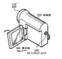
図21は、ビデオカメラの外観を表したものである。このビデオカメラは、例えば、本体部610,この本体部610の前方側面に設けられた被写体撮影用のレンズ620,撮影時のスタート/ストップスイッチ630および表示部640を有している。そして、この表示部640が有機EL表示装置1により構成されている。
(Application example 4)
FIG. 21 shows the appearance of a video camera. This video camera includes, for example, a main body 610, a subject photographing lens 620 provided on the front side surface of the main body 610, a start /
(適用例5)
図22は、携帯電話機の外観を表したものである。この携帯電話機は、例えば、上側筐体710と下側筐体720とを連結部(ヒンジ部)730で連結したものであり、ディスプレイ740,サブディスプレイ750,ピクチャーライト760およびカメラ770を有している。そして、これらのうちのディスプレイ740またはサブディスプレイ750が、有機EL表示装置1により構成されている。
(Application example 5)
FIG. 22 shows the appearance of a mobile phone. For example, the mobile phone is obtained by connecting an
以上、実施の形態、変形例および適用例を挙げて本開示を説明したが、本開示内容はこれらの実施の形態等に限定されず、種々の変形が可能である。例えば、上記第1の実施の形態では、サブ画素10Wにおけるブラックマトリクス16Mの開口幅のみを変更した構成を例示したが、このような構成に限定されず、サブ画素10Wの開口幅が他のサブ画素に比べ、相対的に小さくなっていれば、本開示における効果と同等の効果を得ることができる。例えば、サブ画素10W以外のサブ画素における開口幅を変更してもよいし、サブ画素10Wにおける画素開口幅(第1電極の幅)を変更して透過率を制御するようにしてもよいし、それらの変更制御を組み合わせてもよい。
Although the present disclosure has been described with the embodiment, the modification, and the application example, the present disclosure is not limited to the embodiment and the like, and various modifications can be made. For example, in the first embodiment, the configuration in which only the aperture width of the
また、上記実施の形態等では、各サブ画素が発光素子として、白色発光層を有する白色有機EL素子10aを有する場合について説明したが、これに限定されず、例えば、サブ画素10R,10G,10B内の発光素子としてR,G,Bの各色光を個別に発するものを用いてもよい。また、白色発光層についても、発光色が異なる複数の発光層が積層された構造ではなく、面内方向に複数の発光層を配置した構造であってもよい。更に、上記実施の形態等では、発光素子の一例として自発光型の有機EL素子を挙げて説明したが、自発光型の発光素子に限定されず、例えば液晶表示素子などの発光素子(表示素子)を用いてもよい。
In the above-described embodiment and the like, the case where each sub-pixel has the white
更に、上記実施の形態等では、上記実施の形態等では、第1電極11が陽極(アノード)として機能すると共に第2電極14が陰極(カソード)として機能する場合を例に挙げて説明したが、逆に、第1電極11が陰極として機能すると共に第2電極14が陽極として機能するようにしてもよい。
Furthermore, in the above-described embodiment, the case where the
加えて、上記実施の形態等では、有機EL表示装置1がアクティブマトリクス型である場合について説明したが、アクティブマトリクス駆動のための画素回路の構成は、上記実施の形態等で説明したものに限られない。例えば画素回路において、必要に応じて、容量素子やトランジスタ等を追加したり置き換えたりするようにしてもよい。また、その場合には、画素回路の変更に応じて、上述した走査線駆動回路33、信号線駆動回路34および電源線駆動回路35の他に、必要な駆動回路を追加してもよい。
In addition, in the above-described embodiment, the case where the organic
また、上記実施の形態等では、走査線駆動回路33、信号線駆動回路34および電源線駆動回路35における駆動動作を、タイミング生成回路32が制御する場合について説明したが、他の回路がこれらの駆動動作を制御するようにしてもよい。また、このような走査線駆動回路33、信号線駆動回路34および電源線駆動回路35に対する制御は、ハードウェア(回路)で行われるようにしてもよいし、ソフトウェア(プログラム)で行われるようにしてもよい。
In the above embodiment and the like, the case where the timing generation circuit 32 controls the driving operation in the scanning
尚、本開示の表示装置および電子機器は、以下の(1)〜(20)に記載したような構成であってもよい。
(1)各々が、赤(R),緑(G),青(B)の各色に対応すると共に、第1ないし第3のサブ画素と、前記第1ないし第3のサブ画素よりも高輝度を示す第4のサブ画素とを有する複数の画素を備え、前記複数の画素ではそれぞれ、前記第1ないし第4のサブ画素が、対向配置された一対の基板間に発光素子を有し、前記第1ないし第3のサブ画素では、前記一対の基板のうちの一方の基板側に、対応する色光を選択的に透過させるカラーフィルタが設けられ、前記第4のサブ画素では、前記発光素子から発せられた光の透過率が、前記第4のサブ画素の一部または全部の領域において低減するように構成されている表示装置。
(2)前記一対の基板は、画素駆動回路を有する駆動基板と、透明基板よりなる封止基板とであり、前記カラーフィルタは、前記封止基板側に設けられている上記(1)に記載の表示装置。
(3)前記第1ないし第4のサブ画素に対向して開口を有するブラックマトリクスを備え、前記カラーフィルタは、前記ブラックマトリクスの前記第1ないし第3のサブ画素に対向する開口にそれぞれ設けられ、前記第4のサブ画素では、前記ブラックマトリクスの開口幅が、前記第1ないし第3のサブ画素における各開口幅よりも小さくなっている上記(1)または(2)に記載の表示装置。
(4)前記ブラックマトリクスでは、前記第1ないし第3のサブ画素に対向する開口の形状が方形であり、前記第4のサブ画素に対向する開口の形状が、円形、楕円形またはn角形(nは5以上の整数)である上記(1)〜(3)のいずれかに記載の表示装置。
(5)前記第1ないし第4のサブ画素はいずれも、前記駆動基板上に互いに同一形状の画素電極を有し、前記ブラックマトリクスの各開口の形状は、前記画素電極の基板面に平行な面形状よりも大きくなっている上記(1)〜(4)のいずれかに記載の表示装置。
(6)前記第1ないし第3のサブ画素ではそれぞれ、その透過波長毎に各開口幅が設定されている上記(1)〜(5)のいずれかに記載の表示装置。
(7)前記第1ないし第3のサブ画素における各開口幅が、カラーフィルタ濃度を考慮して設定されている上記(1)〜(6)のいずれかに記載の表示装置。
(8)前記複数の画素は直交する2方向に沿って2次元的に配列され、前記2方向のうちの選択的な一方向において、前記第4のサブ画素における開口幅が、前記第1ないし第3のサブ画素における各開口幅よりも小さくなっている上記(1)〜(7)のいずれかに記載の表示装置。
(9)前記第1ないし第4のサブ画素に対向して開口を有するブラックマトリクスを備え、前記カラーフィルタは、前記ブラックマトリクスの前記第1ないし第3のサブ画素に対向する開口にそれぞれ設けられ、前記ブラックマトリクスの前記第4のサブ画素に対向する開口には、減光フィルタ(Neutral Density filter)が設けられている上記(1)〜(8)のいずれかに記載の表示装置。
(10)前記減光フィルタの透過率は、前記第1ないし第3のサブ画素の各カラーフィルタにおける透過帯域の透過率と同等に設定されている上記(1)〜(9)のいずれかに記載の表示装置。
(11)前記減光フィルタの透過率は、中央部よりも端部においてより低透過率となるように構成されている上記(1)〜(10)のいずれかに記載の表示装置。
(12)前記減光フィルタの透過率は、中央部から端部に向かって段階的に透過率が低くなるように構成されている上記(1)〜(11)のいずれかに記載の表示装置。
(13)前記減光フィルタの透過率は、中央部から端部に向かって連続的に透過率が低くなるように構成されている上記(1)〜(12)のいずれかに記載の表示装置。
(14)前記第1ないし第3のサブ画素ではそれぞれ、その透過波長毎に透過率が設定されている上記(1)〜(13)のいずれかに記載の表示装置。
(15)前記一対の基板は、透明基板上に画素駆動回路を有する駆動基板と、封止基板とであり、前記カラーフィルタは、前記駆動基板側に設けられている上記(1)〜(14)のいずれかに記載の表示装置。
(16)前記駆動基板上の、前記第1ないし第3のサブ画素に対応する領域には前記カラーフィルタ、前記第4のサブ画素に対応する領域には、減光フィルタ(Neutral Density filter)がそれぞれ設けられている上記(1)〜(15)のいずれかに記載の表示装置。
(17)前記第4のサブ画素は、白(W)または黄(Y)の色に対応するものである上記(1)〜(16)のいずれかに記載の表示装置。
(18)前記発光素子は有機電界発光素子である上記(1)〜(17)のいずれかに記載の表示装置。
(19)前記有機電界発光素子は白色光を発する上記(1)〜(18)のいずれかに記載の表示装置。
(20)各々が、赤(R),緑(G),青(B)の各色に対応する第1ないし第3のサブ画素と、前記第1ないし第3のサブ画素よりも高輝度を示す第4のサブ画素とを有する複数の画素を備え、前記複数の画素ではそれぞれ、前記第1ないし第4のサブ画素が、対向配置された一対の基板間に発光素子を有し、前記第1ないし第3のサブ画素では、前記一対の基板のうちの一方の基板側に、対応する色光を選択的に透過させるカラーフィルタが設けられ、前記第4のサブ画素では、前記発光素子から発せられた光の透過率が、前記第4のサブ画素の一部または全部の領域において低減するように構成されている表示装置を有する電子機器。
Note that the display device and the electronic apparatus according to the present disclosure may be configured as described in the following (1) to (20).
(1) Each corresponds to each color of red (R), green (G), and blue (B), and has higher luminance than the first to third subpixels and the first to third subpixels. A plurality of pixels each having a fourth sub-pixel, and each of the plurality of pixels includes a light-emitting element between a pair of opposed substrates. In the first to third sub-pixels, a color filter that selectively transmits corresponding color light is provided on one of the pair of substrates, and in the fourth sub-pixel, the light emitting element A display device configured to reduce a transmittance of emitted light in a part or all of a region of the fourth sub-pixel.
(2) The pair of substrates is a driving substrate having a pixel driving circuit and a sealing substrate made of a transparent substrate, and the color filter is provided on the sealing substrate side. Display device.
(3) A black matrix having an opening facing the first to fourth sub-pixels is provided, and the color filter is provided in each opening facing the first to third sub-pixels of the black matrix. The display device according to (1) or (2), wherein in the fourth sub-pixel, an opening width of the black matrix is smaller than each opening width in the first to third sub-pixels.
(4) In the black matrix, the shape of the opening facing the first to third subpixels is a square, and the shape of the opening facing the fourth subpixel is a circle, an ellipse, or an n-square ( The display device according to any one of (1) to (3), wherein n is an integer of 5 or more.
(5) Each of the first to fourth subpixels has a pixel electrode having the same shape on the driving substrate, and the shape of each opening of the black matrix is parallel to the substrate surface of the pixel electrode. The display device according to any one of (1) to (4), wherein the display device is larger than a surface shape.
(6) The display device according to any one of (1) to (5), wherein each aperture width is set for each transmission wavelength in each of the first to third subpixels.
(7) The display device according to any one of (1) to (6), wherein each aperture width in the first to third sub-pixels is set in consideration of a color filter density.
(8) The plurality of pixels are two-dimensionally arrayed along two orthogonal directions, and an opening width in the fourth sub-pixel in the selective one of the two directions is the first to The display device according to any one of (1) to (7), which is smaller than each opening width in the third sub-pixel.
(9) A black matrix having an opening facing the first to fourth sub-pixels is provided, and the color filter is provided in each opening facing the first to third sub-pixels of the black matrix. The display device according to any one of (1) to (8), wherein a neutral density filter is provided in an opening facing the fourth sub-pixel of the black matrix.
(10) The transmittance of the neutral density filter is set to be equal to the transmittance of the transmission band in each color filter of the first to third sub-pixels. The display device described.
(11) The display device according to any one of (1) to (10), wherein the transmittance of the neutral density filter is configured to be lower at the end than at the center.
(12) The display device according to any one of (1) to (11), wherein the transmittance of the neutral density filter is configured such that the transmittance decreases stepwise from a central portion toward an end portion. .
(13) The display device according to any one of (1) to (12), wherein the transmittance of the neutral density filter is configured such that the transmittance continuously decreases from the center toward the end. .
(14) The display device according to any one of (1) to (13), wherein a transmittance is set for each transmission wavelength of each of the first to third subpixels.
(15) The pair of substrates includes a drive substrate having a pixel drive circuit on a transparent substrate and a sealing substrate, and the color filter is provided on the drive substrate side (1) to (14). ).
(16) On the drive substrate, the color filter is provided in a region corresponding to the first to third sub-pixels, and a neutral density filter is provided in a region corresponding to the fourth sub-pixel. The display device according to any one of (1) to (15), each provided.
(17) The display device according to any one of (1) to (16), wherein the fourth sub-pixel corresponds to a color of white (W) or yellow (Y).
(18) The display device according to any one of (1) to (17), wherein the light emitting element is an organic electroluminescent element.
(19) The display device according to any one of (1) to (18), wherein the organic electroluminescent element emits white light.
(20) Each of the first to third subpixels corresponding to each color of red (R), green (G), and blue (B) and higher brightness than the first to third subpixels. A plurality of pixels having a fourth sub-pixel, and each of the plurality of pixels includes a light-emitting element between a pair of substrates opposed to each other, and In the third sub-pixel, a color filter that selectively transmits the corresponding color light is provided on one of the pair of substrates, and the fourth sub-pixel emits light from the light-emitting element. An electronic apparatus having a display device configured to reduce light transmittance in a part or all of the region of the fourth sub-pixel.
1,2…有機EL表示装置、10…駆動基板、10a…白色有機EL素子、10R,10G,10B,10W…サブ画素、30…駆動回路,30A,31A…映像信号、30B…同期信号、31…映像信号処理回路、310…変換処理部、32…タイミング生成回路、32A…制御信号、33…走査線駆動回路、34…信号線駆動回路、35…電源線駆動回路、11…第1電極、12…画素間絶縁膜、13…有機層、14…第2電極、15…保護膜、16…カラーフィルタ層、16M…ブラックマトリクス、M1,Mw…開口、16R…赤色フィルタ、16G…緑色フィルタ、16B…青色フィルタ、17…NDフィルタ、LBM,LBM(W)…開口幅、LP…開口幅、d,dw…開口マージン、WSL…走査線、DTL,DTLr,DTLg,DTLb,DTLw…信号線、DSL…電源線、Tr1…書き込みトランジスタ、Tr2…駆動トランジスタ、Cs…保持容量素子、Id…電流、Vg…ゲート電位、Vs…ソース電位、Vgs…ゲート−ソース間電圧、VSS…固定電位。
DESCRIPTION OF
Claims (16)
前記第1ないし第4のサブ画素のそれぞれに対向して第1ないし第4の開口を有するブラックマトリクスと
を備え、
前記複数の画素ではそれぞれ、
前記第1ないし第4のサブ画素が、対向配置された一対の基板間に有機電界発光素子を有し、
前記ブラックマトリクスでは、
前記第1ないし第3の開口に、R,G,Bの各色に対応するカラーフィルタが設けられ、
前記第1ないし第4の開口の各形状は、前記有機電界発光素子の画素電極の基板面に平行な面形状よりも大きく、
前記第4の開口の幅は、前記第1ないし第3の開口の幅よりも狭く、かつ
前記第4の開口の幅と前記画素電極の幅との差は、前記第1ないし第3の開口のそれぞれの幅と前記画素電極の幅との差よりも小さい
表示装置。 Each red (R), green (G), and a fourth showing the first to third sub-pixels that correspond to the respective colors of blue (B), the first to third luminance higher than sub-pixel a plurality of pixels and a subpixel,
A black matrix having first to fourth openings facing each of the first to fourth sub-pixels ,
In each of the plurality of pixels,
The first to fourth sub-pixels each include an organic electroluminescent element between a pair of substrates disposed opposite to each other;
In the black matrix,
The first to third openings are provided with color filters corresponding to R, G, and B colors,
Each shape of the first to fourth openings is larger than a surface shape parallel to the substrate surface of the pixel electrode of the organic electroluminescent element,
The width of the fourth opening is narrower than the width of the first to third openings; and
The difference between the width of the fourth opening and the width of the pixel electrode is smaller than the difference between the width of each of the first to third openings and the width of the pixel electrode .
前記カラーフィルタは、前記封止基板側に設けられている
請求項1に記載の表示装置。 The pair of substrates are a driving substrate having a pixel driving circuit and a sealing substrate made of a transparent substrate,
The display device according to claim 1, wherein the color filter is provided on the sealing substrate side.
前記第1ないし第3の開口のそれぞれの形状が方形であり、
前記第4の開口の形状が、円形、楕円形またはn角形(nは5以上の整数)である
請求項1または2に記載の表示装置。 In the black matrix,
Each of the first to third openings has a square shape,
Wherein the shape of the fourth opening is circular, the display device according to claim 1 or 2 which is oval or n-angular (n is an integer of 5 or more).
請求項1ないし3のいずれか1つに記載の表示装置。The display device according to any one of claims 1 to 3.
請求項1ないし4のいずれか1つに記載の表示装置。 Wherein each of the widths of the first to third openings, the display device according to any one of claims 1 are set for respective transmission wavelength 4.
請求項1ないし5のいずれか1つに記載の表示装置。 Display device according to any one of the respective widths of the first to third openings, claims 1 and is set in consideration of the color filter density 5.
前記2方向の各方向において、前記第4の開口の幅が、前記第1ないし第3の開口のそれぞれの幅よりも小さくなっている
請求項1ないし6のいずれか1つに記載の表示装置。 The plurality of pixels are two-dimensionally arranged along two orthogonal directions,
In each direction of the two directions, the width of the fourth opening, a display device according to any one of the first to third of claims 1 is smaller than the width of each of the openings 6 .
前記カラーフィルタは、前記駆動基板側に設けられている
請求項1に記載の表示装置。 The pair of substrates is a driving substrate having a pixel driving circuit on a transparent substrate, and a sealing substrate,
The display device according to claim 1, wherein the color filter is provided on the drive substrate side.
請求項1ないし8のいずれか1つに記載の表示装置。 The fourth sub-pixel, a white (W) or the display device according to any one of claims 1 to 8 and corresponds to the color yellow (Y).
請求項9に記載の表示装置。 The display device according to claim 9 , wherein the organic electroluminescent element emits white light.
前記第1ないし第4のサブ画素のそれぞれに対向して第1ないし第4の開口を有するブラックマトリクスとA black matrix having first to fourth openings facing each of the first to fourth sub-pixels;
を備え、With
前記複数の画素ではそれぞれ、In each of the plurality of pixels,
前記第1ないし第4のサブ画素が、対向配置された一対の基板間に有機電界発光素子を有し、The first to fourth sub-pixels each include an organic electroluminescent element between a pair of substrates disposed opposite to each other;
前記ブラックマトリクスでは、In the black matrix,
前記第1ないし第3の開口に、R,G,Bの各色に対応するカラーフィルタが設けられ、The first to third openings are provided with color filters corresponding to R, G, and B colors,
前記第4の開口には、中央部よりも端部においてより低透過率となるように構成された減光フィルタ(Neutral Density filter)が設けられているThe fourth opening is provided with a neutral density filter configured to have a lower transmittance at the end than at the center.
表示装置。Display device.
請求項11に記載の表示装置。 Transmittance of the neutral density filter, a display device according to claim 11 which is stepwise decreased toward the end portion from the center portion.
請求項11または12に記載の表示装置。 The display device according to claim 11, wherein the transmittance of the neutral density filter continuously decreases from a central portion toward an end portion.
請求項11ないし13のいずれか1つに記載の表示装置。 14. The display device according to claim 11 , wherein a transmittance is set for each of the transmission wavelengths in each of the first to third openings.
前記第1ないし第4のサブ画素のそれぞれに対向して第1ないし第4の開口を有するブラックマトリクスと
を備え、
前記複数の画素ではそれぞれ、
前記第1ないし第4のサブ画素が、対向配置された一対の基板間に有機電界発光素子を有し、
前記ブラックマトリクスでは、
前記第1ないし第3の開口に、R,G,Bの各色に対応するカラーフィルタが設けられ、
前記第1ないし第4の開口の各形状は、前記有機電界発光素子の画素電極の基板面に平行な面形状よりも大きく、
前記第4の開口の幅は、前記第1ないし第3の開口の幅よりも狭く、かつ
前記第4の開口の幅と前記画素電極の幅との差は、前記第1ないし第3の開口のそれぞれの幅と前記画素電極の幅との差よりも小さい
表示装置を有する電子機器。 Each red (R), green (G), and a fourth showing the first to third sub-pixels that correspond to the respective colors of blue (B), the first to third luminance higher than sub-pixel a plurality of pixels and a subpixel,
A black matrix having first to fourth openings facing each of the first to fourth sub-pixels ,
In each of the plurality of pixels,
The first to fourth sub-pixels each include an organic electroluminescent element between a pair of substrates disposed opposite to each other;
In the black matrix,
The first to third openings are provided with color filters corresponding to R, G, and B colors,
Each shape of the first to fourth openings is larger than a surface shape parallel to the substrate surface of the pixel electrode of the organic electroluminescent element,
The width of the fourth opening is narrower than the width of the first to third openings; and
An electronic apparatus having a display device , wherein a difference between the width of the fourth opening and the width of the pixel electrode is smaller than a difference between the width of each of the first to third openings and the width of the pixel electrode .
前記第1ないし第4のサブ画素のそれぞれに対向して第1ないし第4の開口を有するブラックマトリクスとA black matrix having first to fourth openings facing each of the first to fourth sub-pixels;
を備え、With
前記複数の画素ではそれぞれ、In each of the plurality of pixels,
前記第1ないし第4のサブ画素が、対向配置された一対の基板間に有機電界発光素子を有し、The first to fourth sub-pixels each include an organic electroluminescent element between a pair of substrates disposed opposite to each other;
前記ブラックマトリクスでは、In the black matrix,
前記第1ないし第3の開口に、R,G,Bの各色に対応するカラーフィルタが設けられ、The first to third openings are provided with color filters corresponding to R, G, and B colors,
前記第4の開口には、中央部よりも端部においてより低透過率となるように構成された減光フィルタ(Neutral Density filter)が設けられているThe fourth opening is provided with a neutral density filter configured to have a lower transmittance at the end than at the center.
表示装置を有する電子機器。An electronic device having a display device.
Priority Applications (5)
| Application Number | Priority Date | Filing Date | Title |
|---|---|---|---|
| JP2011219054A JP5927476B2 (en) | 2011-10-03 | 2011-10-03 | Display device and electronic device |
| US14/346,922 US9123669B2 (en) | 2011-10-03 | 2012-09-25 | Display unit and electronic apparatus |
| PCT/JP2012/074550 WO2013051428A1 (en) | 2011-10-03 | 2012-09-25 | Display device and electronic device |
| CN201280047430.8A CN103828486B (en) | 2011-10-03 | 2012-09-25 | Display unit and electronic equipment |
| KR1020147007002A KR101913455B1 (en) | 2011-10-03 | 2012-09-25 | Display device and electronic device |
Applications Claiming Priority (1)
| Application Number | Priority Date | Filing Date | Title |
|---|---|---|---|
| JP2011219054A JP5927476B2 (en) | 2011-10-03 | 2011-10-03 | Display device and electronic device |
Publications (3)
| Publication Number | Publication Date |
|---|---|
| JP2013080584A JP2013080584A (en) | 2013-05-02 |
| JP2013080584A5 JP2013080584A5 (en) | 2014-10-23 |
| JP5927476B2 true JP5927476B2 (en) | 2016-06-01 |
Family
ID=48043590
Family Applications (1)
| Application Number | Title | Priority Date | Filing Date |
|---|---|---|---|
| JP2011219054A Active JP5927476B2 (en) | 2011-10-03 | 2011-10-03 | Display device and electronic device |
Country Status (5)
| Country | Link |
|---|---|
| US (1) | US9123669B2 (en) |
| JP (1) | JP5927476B2 (en) |
| KR (1) | KR101913455B1 (en) |
| CN (1) | CN103828486B (en) |
| WO (1) | WO2013051428A1 (en) |
Families Citing this family (45)
| Publication number | Priority date | Publication date | Assignee | Title |
|---|---|---|---|---|
| JP6057647B2 (en) * | 2012-09-27 | 2017-01-11 | 三菱電機株式会社 | Display device |
| KR101997745B1 (en) * | 2013-01-25 | 2019-07-09 | 삼성디스플레이 주식회사 | Liquid crystal display |
| JP2015014670A (en) | 2013-07-04 | 2015-01-22 | 株式会社ジャパンディスプレイ | Liquid crystal display device |
| KR102190843B1 (en) * | 2013-07-09 | 2020-12-15 | 삼성디스플레이 주식회사 | Unit pixel and organic light emitting display device having the same |
| JP2015037062A (en) * | 2013-08-15 | 2015-02-23 | ソニー株式会社 | Display device and electronic apparatus |
| JP2015079205A (en) | 2013-10-18 | 2015-04-23 | 株式会社ジャパンディスプレイ | Display device |
| JP6257259B2 (en) | 2013-10-18 | 2018-01-10 | 株式会社ジャパンディスプレイ | Display device |
| KR102274586B1 (en) * | 2013-10-31 | 2021-07-07 | 엘지디스플레이 주식회사 | Transparent organic light emitting display device and method of decreasing reflection of light at the same |
| KR102255809B1 (en) * | 2013-12-02 | 2021-05-24 | 엘지디스플레이 주식회사 | Organic Light Emitting Display Device |
| KR102196889B1 (en) * | 2013-12-13 | 2020-12-30 | 엘지디스플레이 주식회사 | Organic Light Emitting Diode Display Device and Method for Manufacturing The Same |
| JP2015125365A (en) | 2013-12-27 | 2015-07-06 | 株式会社ジャパンディスプレイ | Liquid crystal display |
| JP2015144087A (en) | 2014-01-31 | 2015-08-06 | ソニー株式会社 | Organic electroluminescent device and electronic apparatus |
| KR102274580B1 (en) * | 2014-04-30 | 2021-07-06 | 엘지디스플레이 주식회사 | Organic light emitting display and method of manufacturing the same |
| US10388705B2 (en) * | 2014-05-27 | 2019-08-20 | Lg Display Co., Ltd. | Display panel and method for manufacturing thereof |
| JP2016004101A (en) * | 2014-06-16 | 2016-01-12 | 株式会社ジャパンディスプレイ | Display device |
| CN106537486B (en) | 2014-07-31 | 2020-09-15 | 株式会社半导体能源研究所 | Display device and electronic device |
| JP2016042449A (en) * | 2014-08-19 | 2016-03-31 | 株式会社ジャパンディスプレイ | Display device |
| KR102392020B1 (en) * | 2014-09-30 | 2022-04-27 | 엘지디스플레이 주식회사 | Organic light emitting display device |
| CN104299982A (en) * | 2014-10-20 | 2015-01-21 | 深圳市华星光电技术有限公司 | Color display device |
| JP2016133590A (en) * | 2015-01-19 | 2016-07-25 | ソニー株式会社 | Display device and electronic apparatus |
| KR20160095701A (en) * | 2015-02-03 | 2016-08-12 | 삼성디스플레이 주식회사 | Liquid crystal display device and manufacturing method thereof |
| JP6517597B2 (en) * | 2015-06-10 | 2019-05-22 | 株式会社ジャパンディスプレイ | Display device |
| KR102572407B1 (en) * | 2015-07-22 | 2023-08-30 | 엘지디스플레이 주식회사 | Thin Film Transistor Array Substrate And Organic Light Emitting Diode Display Device Including The Same |
| KR102575459B1 (en) * | 2015-07-31 | 2023-09-06 | 엘지디스플레이 주식회사 | Organic light emitting display device and method for fabricating thereof |
| KR102403000B1 (en) | 2015-10-01 | 2022-05-30 | 삼성디스플레이 주식회사 | Organic light-emitting display apparatus |
| CN105425451B (en) * | 2015-11-23 | 2018-08-14 | 上海中航光电子有限公司 | A kind of color membrane substrates, display panel and display device |
| KR102578835B1 (en) * | 2016-07-29 | 2023-09-14 | 엘지디스플레이 주식회사 | Backplane Substrate and Organic Light Emitting Display Device Using the Same |
| CN106125179B (en) * | 2016-08-29 | 2019-02-26 | 武汉华星光电技术有限公司 | Display device and its optical filter |
| KR102600694B1 (en) * | 2016-10-28 | 2023-11-09 | 엘지디스플레이 주식회사 | Display device having a white emitting area |
| CN107331682A (en) * | 2017-06-23 | 2017-11-07 | 安徽熙泰智能科技有限公司 | A kind of silicon substrate OLED micro display chips and its colorization implementation method |
| KR102393319B1 (en) | 2017-07-04 | 2022-05-02 | 삼성디스플레이 주식회사 | Organic light emitting display device |
| JP2019114484A (en) * | 2017-12-26 | 2019-07-11 | ソニーセミコンダクタソリューションズ株式会社 | Display element and electronic device |
| CN111492271B (en) * | 2017-12-29 | 2022-06-14 | 索尼半导体解决方案公司 | Light emitting module, display device, and methods of manufacturing light emitting module and display device |
| KR102490894B1 (en) * | 2018-02-08 | 2023-01-25 | 삼성디스플레이 주식회사 | Organic light emitting display apparatus |
| US11003287B2 (en) * | 2018-03-30 | 2021-05-11 | Sharp Kabushiki Kaisha | Touch sensor for display with improved viewing angle uniformity |
| WO2019216198A1 (en) * | 2018-05-11 | 2019-11-14 | ソニーセミコンダクタソリューションズ株式会社 | Display apparatus, display apparatus manufacturing method, and electronic device |
| TWI678009B (en) * | 2018-06-22 | 2019-11-21 | 友達光電股份有限公司 | Display panel and manufacturing method thereof |
| CN108807490B (en) * | 2018-06-29 | 2021-06-01 | 武汉天马微电子有限公司 | Organic light emitting display panel and display device |
| KR102587657B1 (en) * | 2018-09-28 | 2023-10-12 | 엘지디스플레이 주식회사 | Display apparatus including light receving pixel area |
| CN110531550A (en) * | 2019-09-03 | 2019-12-03 | 武汉天马微电子有限公司 | A kind of display panel and display device |
| CN112542484A (en) * | 2019-09-20 | 2021-03-23 | 北京小米移动软件有限公司 | Display panel, display screen and electronic equipment |
| TWI710826B (en) * | 2019-11-29 | 2020-11-21 | 友達光電股份有限公司 | Display panel |
| JP7458847B2 (en) * | 2020-03-24 | 2024-04-01 | キヤノン株式会社 | Display and electronic devices |
| CN113140603B (en) * | 2021-04-13 | 2022-06-14 | 武汉天马微电子有限公司 | Display panel and display device |
| CN113328047B (en) * | 2021-06-02 | 2022-06-10 | 武汉天马微电子有限公司 | Display panel, manufacturing method thereof and display device |
Family Cites Families (18)
| Publication number | Priority date | Publication date | Assignee | Title |
|---|---|---|---|---|
| US5073008A (en) * | 1987-12-11 | 1991-12-17 | Fuji Photo Film Co., Ltd. | Multicolor interference filters with side surfaces to prevent entry of undesirable light |
| JPH02118521A (en) | 1989-09-28 | 1990-05-02 | Seiko Epson Corp | Liquid crystal display device |
| JP3921302B2 (en) * | 1998-11-11 | 2007-05-30 | 松下電器産業株式会社 | Color filter and time-division color display using it |
| JP2004252309A (en) * | 2003-02-21 | 2004-09-09 | Seiko Epson Corp | Electrooptical panel and electronic equipment |
| JP4005948B2 (en) | 2003-06-18 | 2007-11-14 | トヨタ自動車株式会社 | Method and apparatus for stripping conductive film of conductive wire |
| US7560862B2 (en) | 2004-10-22 | 2009-07-14 | Eastman Kodak Company | White OLEDs with a color-compensated electroluminescent unit |
| JP4684046B2 (en) | 2005-03-30 | 2011-05-18 | 三洋電機株式会社 | Display device |
| JP4828881B2 (en) | 2005-07-15 | 2011-11-30 | 東芝モバイルディスプレイ株式会社 | Organic EL display device |
| US7294959B2 (en) * | 2005-10-24 | 2007-11-13 | Eastman Kodak Company | OLED device having improved contrast |
| CN101958098B (en) * | 2006-06-19 | 2016-03-16 | 夏普株式会社 | Display device |
| JP4529988B2 (en) * | 2007-03-08 | 2010-08-25 | セイコーエプソン株式会社 | Light emitting device and electronic device |
| US7741770B2 (en) * | 2007-10-05 | 2010-06-22 | Global Oled Technology Llc | LED device having improved light output |
| EP2120275A3 (en) * | 2008-05-16 | 2012-08-22 | Semiconductor Energy Laboratory Co, Ltd. | Light-emitting element, lighting apparatus, light-emitting device, electronic appliance, and display |
| KR20100068074A (en) * | 2008-12-12 | 2010-06-22 | 삼성전자주식회사 | Organic light emitting devicce |
| JP5506226B2 (en) * | 2009-03-31 | 2014-05-28 | エルジー ディスプレイ カンパニー リミテッド | Image display device |
| JP5293497B2 (en) * | 2009-08-18 | 2013-09-18 | ソニー株式会社 | Display device |
| KR101125570B1 (en) * | 2009-12-04 | 2012-03-22 | 삼성모바일디스플레이주식회사 | Organic light emitting diode device |
| US8502445B2 (en) * | 2011-07-18 | 2013-08-06 | Universal Display Corporation | RGBW OLED display for extended lifetime and reduced power consumption |
-
2011
- 2011-10-03 JP JP2011219054A patent/JP5927476B2/en active Active
-
2012
- 2012-09-25 US US14/346,922 patent/US9123669B2/en active Active
- 2012-09-25 CN CN201280047430.8A patent/CN103828486B/en active Active
- 2012-09-25 KR KR1020147007002A patent/KR101913455B1/en active IP Right Grant
- 2012-09-25 WO PCT/JP2012/074550 patent/WO2013051428A1/en active Application Filing
Also Published As
| Publication number | Publication date |
|---|---|
| JP2013080584A (en) | 2013-05-02 |
| CN103828486A (en) | 2014-05-28 |
| US20140231790A1 (en) | 2014-08-21 |
| US9123669B2 (en) | 2015-09-01 |
| CN103828486B (en) | 2016-08-31 |
| WO2013051428A1 (en) | 2013-04-11 |
| KR101913455B1 (en) | 2018-10-30 |
| KR20140083988A (en) | 2014-07-04 |
Similar Documents
| Publication | Publication Date | Title |
|---|---|---|
| JP5927476B2 (en) | Display device and electronic device | |
| US9508285B2 (en) | Pixel array, metal mask, electro optical device and electric apparatus | |
| US8872842B2 (en) | Display device and electronics apparatus | |
| US10032403B2 (en) | Electro optical device, electric apparatus and pixel rendering method | |
| US10553143B2 (en) | Display apparatus and electronic appliance | |
| CN108269944B (en) | Display device | |
| US11903285B2 (en) | Display device and electronic device with peripheral connection to cathode electrode | |
| US20210057494A1 (en) | Display device | |
| KR20190064004A (en) | Organic light emitting display device | |
| US8736526B2 (en) | Display unit with organic light emitting devices | |
| US9184416B2 (en) | Organic electro luminescent display device | |
| CN111326673B (en) | Display device | |
| JPWO2019026511A1 (en) | Display device, display device manufacturing method, and electronic device | |
| KR102646913B1 (en) | Organic light emitting display device | |
| WO2020145148A1 (en) | Display device | |
| JP7050772B2 (en) | Display devices and electronic devices | |
| JP7312697B2 (en) | Displays and electronics | |
| WO2019203027A1 (en) | Display device and electronic apparatus | |
| KR102593451B1 (en) | Organic Light Emitting Display Device and Method of Manufacturing the same | |
| KR102413199B1 (en) | Organic light emitting diode display device | |
| US20230247864A1 (en) | Display device and electronic device | |
| WO2020071026A1 (en) | Display device and electronic device | |
| KR20190062853A (en) | Organic light emitting display device |
Legal Events
| Date | Code | Title | Description |
|---|---|---|---|
| A521 | Request for written amendment filed |
Free format text: JAPANESE INTERMEDIATE CODE: A523 Effective date: 20140904 |
|
| A621 | Written request for application examination |
Free format text: JAPANESE INTERMEDIATE CODE: A621 Effective date: 20140904 |
|
| A711 | Notification of change in applicant |
Free format text: JAPANESE INTERMEDIATE CODE: A712 Effective date: 20150327 |
|
| A131 | Notification of reasons for refusal |
Free format text: JAPANESE INTERMEDIATE CODE: A131 Effective date: 20150819 |
|
| A521 | Request for written amendment filed |
Free format text: JAPANESE INTERMEDIATE CODE: A523 Effective date: 20150910 |
|
| TRDD | Decision of grant or rejection written | ||
| A01 | Written decision to grant a patent or to grant a registration (utility model) |
Free format text: JAPANESE INTERMEDIATE CODE: A01 Effective date: 20160223 |
|
| A61 | First payment of annual fees (during grant procedure) |
Free format text: JAPANESE INTERMEDIATE CODE: A61 Effective date: 20160304 |
|
| R150 | Certificate of patent or registration of utility model |
Ref document number: 5927476 Country of ref document: JP Free format text: JAPANESE INTERMEDIATE CODE: R150 |
|
| R250 | Receipt of annual fees |
Free format text: JAPANESE INTERMEDIATE CODE: R250 |
|
| R250 | Receipt of annual fees |
Free format text: JAPANESE INTERMEDIATE CODE: R250 |
|
| R250 | Receipt of annual fees |
Free format text: JAPANESE INTERMEDIATE CODE: R250 |
|
| R250 | Receipt of annual fees |
Free format text: JAPANESE INTERMEDIATE CODE: R250 |
|
| S303 | Written request for registration of pledge or change of pledge |
Free format text: JAPANESE INTERMEDIATE CODE: R316303 |
|
| R350 | Written notification of registration of transfer |
Free format text: JAPANESE INTERMEDIATE CODE: R350 |
|
| R250 | Receipt of annual fees |
Free format text: JAPANESE INTERMEDIATE CODE: R250 |
|
| S803 | Written request for registration of cancellation of provisional registration |
Free format text: JAPANESE INTERMEDIATE CODE: R316803 |
|
| R350 | Written notification of registration of transfer |
Free format text: JAPANESE INTERMEDIATE CODE: R350 |