JP7350903B2 - Tft回路基板 - Google Patents
Tft回路基板 Download PDFInfo
- Publication number
- JP7350903B2 JP7350903B2 JP2022000800A JP2022000800A JP7350903B2 JP 7350903 B2 JP7350903 B2 JP 7350903B2 JP 2022000800 A JP2022000800 A JP 2022000800A JP 2022000800 A JP2022000800 A JP 2022000800A JP 7350903 B2 JP7350903 B2 JP 7350903B2
- Authority
- JP
- Japan
- Prior art keywords
- film
- tft
- insulating film
- oxide semiconductor
- gate
- Prior art date
- Legal status (The legal status is an assumption and is not a legal conclusion. Google has not performed a legal analysis and makes no representation as to the accuracy of the status listed.)
- Active
Links
- 239000004065 semiconductor Substances 0.000 claims description 90
- 239000011229 interlayer Substances 0.000 claims description 67
- 239000010410 layer Substances 0.000 claims description 20
- 239000012528 membrane Substances 0.000 claims 1
- 239000010408 film Substances 0.000 description 260
- 238000001312 dry etching Methods 0.000 description 32
- VYPSYNLAJGMNEJ-UHFFFAOYSA-N Silicium dioxide Chemical compound O=[Si]=O VYPSYNLAJGMNEJ-UHFFFAOYSA-N 0.000 description 24
- 229910052814 silicon oxide Inorganic materials 0.000 description 24
- 229910021420 polycrystalline silicon Inorganic materials 0.000 description 21
- 239000000460 chlorine Substances 0.000 description 19
- 239000004973 liquid crystal related substance Substances 0.000 description 18
- 238000000034 method Methods 0.000 description 18
- 239000000758 substrate Substances 0.000 description 18
- 230000004888 barrier function Effects 0.000 description 17
- 229910052751 metal Inorganic materials 0.000 description 17
- 239000002184 metal Substances 0.000 description 17
- 229910000838 Al alloy Inorganic materials 0.000 description 16
- 238000005530 etching Methods 0.000 description 16
- ZAMOUSCENKQFHK-UHFFFAOYSA-N Chlorine atom Chemical compound [Cl] ZAMOUSCENKQFHK-UHFFFAOYSA-N 0.000 description 15
- 229910052801 chlorine Inorganic materials 0.000 description 15
- 230000008569 process Effects 0.000 description 15
- 229910052581 Si3N4 Inorganic materials 0.000 description 11
- HQVNEWCFYHHQES-UHFFFAOYSA-N silicon nitride Chemical compound N12[Si]34N5[Si]62N3[Si]51N64 HQVNEWCFYHHQES-UHFFFAOYSA-N 0.000 description 11
- YCKRFDGAMUMZLT-UHFFFAOYSA-N Fluorine atom Chemical compound [F] YCKRFDGAMUMZLT-UHFFFAOYSA-N 0.000 description 10
- 229910052731 fluorine Inorganic materials 0.000 description 10
- 239000011737 fluorine Substances 0.000 description 10
- 239000010953 base metal Substances 0.000 description 8
- 239000011521 glass Substances 0.000 description 8
- 239000007789 gas Substances 0.000 description 6
- XLOMVQKBTHCTTD-UHFFFAOYSA-N Zinc monoxide Chemical compound [Zn]=O XLOMVQKBTHCTTD-UHFFFAOYSA-N 0.000 description 5
- 230000015572 biosynthetic process Effects 0.000 description 5
- 230000001681 protective effect Effects 0.000 description 5
- 229910021417 amorphous silicon Inorganic materials 0.000 description 4
- BOTDANWDWHJENH-UHFFFAOYSA-N Tetraethyl orthosilicate Chemical compound CCO[Si](OCC)(OCC)OCC BOTDANWDWHJENH-UHFFFAOYSA-N 0.000 description 3
- 239000001257 hydrogen Substances 0.000 description 3
- 229910052739 hydrogen Inorganic materials 0.000 description 3
- 239000000463 material Substances 0.000 description 3
- 239000000203 mixture Substances 0.000 description 3
- 239000011368 organic material Substances 0.000 description 3
- 239000011347 resin Substances 0.000 description 3
- 229920005989 resin Polymers 0.000 description 3
- 239000010409 thin film Substances 0.000 description 3
- 239000011787 zinc oxide Substances 0.000 description 3
- 229910000789 Aluminium-silicon alloy Inorganic materials 0.000 description 2
- KZBUYRJDOAKODT-UHFFFAOYSA-N Chlorine Chemical compound ClCl KZBUYRJDOAKODT-UHFFFAOYSA-N 0.000 description 2
- GYHNNYVSQQEPJS-UHFFFAOYSA-N Gallium Chemical compound [Ga] GYHNNYVSQQEPJS-UHFFFAOYSA-N 0.000 description 2
- UFHFLCQGNIYNRP-UHFFFAOYSA-N Hydrogen Chemical compound [H][H] UFHFLCQGNIYNRP-UHFFFAOYSA-N 0.000 description 2
- NIXOWILDQLNWCW-UHFFFAOYSA-N acrylic acid group Chemical group C(C=C)(=O)O NIXOWILDQLNWCW-UHFFFAOYSA-N 0.000 description 2
- 239000000853 adhesive Substances 0.000 description 2
- 230000001070 adhesive effect Effects 0.000 description 2
- 229910003481 amorphous carbon Inorganic materials 0.000 description 2
- 238000000231 atomic layer deposition Methods 0.000 description 2
- 230000000903 blocking effect Effects 0.000 description 2
- 239000003990 capacitor Substances 0.000 description 2
- 230000008859 change Effects 0.000 description 2
- 230000000052 comparative effect Effects 0.000 description 2
- 238000010586 diagram Methods 0.000 description 2
- 229910052733 gallium Inorganic materials 0.000 description 2
- 229910052738 indium Inorganic materials 0.000 description 2
- APFVFJFRJDLVQX-UHFFFAOYSA-N indium atom Chemical compound [In] APFVFJFRJDLVQX-UHFFFAOYSA-N 0.000 description 2
- 229910010272 inorganic material Inorganic materials 0.000 description 2
- 239000011147 inorganic material Substances 0.000 description 2
- 238000005468 ion implantation Methods 0.000 description 2
- 238000004519 manufacturing process Methods 0.000 description 2
- 239000011159 matrix material Substances 0.000 description 2
- 239000000565 sealant Substances 0.000 description 2
- 238000004544 sputter deposition Methods 0.000 description 2
- 229910016570 AlCu Inorganic materials 0.000 description 1
- 239000004642 Polyimide Substances 0.000 description 1
- ATJFFYVFTNAWJD-UHFFFAOYSA-N Tin Chemical compound [Sn] ATJFFYVFTNAWJD-UHFFFAOYSA-N 0.000 description 1
- -1 Zinc Oxide Nitride Chemical class 0.000 description 1
- 230000009471 action Effects 0.000 description 1
- 229910045601 alloy Inorganic materials 0.000 description 1
- 239000000956 alloy Substances 0.000 description 1
- PNEYBMLMFCGWSK-UHFFFAOYSA-N aluminium oxide Inorganic materials [O-2].[O-2].[O-2].[Al+3].[Al+3] PNEYBMLMFCGWSK-UHFFFAOYSA-N 0.000 description 1
- 229910052804 chromium Inorganic materials 0.000 description 1
- 150000001875 compounds Chemical class 0.000 description 1
- 239000000470 constituent Substances 0.000 description 1
- 230000007423 decrease Effects 0.000 description 1
- 230000000694 effects Effects 0.000 description 1
- 230000014509 gene expression Effects 0.000 description 1
- 150000002431 hydrogen Chemical class 0.000 description 1
- 239000012535 impurity Substances 0.000 description 1
- AMGQUBHHOARCQH-UHFFFAOYSA-N indium;oxotin Chemical compound [In].[Sn]=O AMGQUBHHOARCQH-UHFFFAOYSA-N 0.000 description 1
- 238000009413 insulation Methods 0.000 description 1
- 230000003993 interaction Effects 0.000 description 1
- 230000008018 melting Effects 0.000 description 1
- 238000002844 melting Methods 0.000 description 1
- 150000002739 metals Chemical class 0.000 description 1
- 229910052750 molybdenum Inorganic materials 0.000 description 1
- 230000003287 optical effect Effects 0.000 description 1
- TWNQGVIAIRXVLR-UHFFFAOYSA-N oxo(oxoalumanyloxy)alumane Chemical compound O=[Al]O[Al]=O TWNQGVIAIRXVLR-UHFFFAOYSA-N 0.000 description 1
- 238000002161 passivation Methods 0.000 description 1
- 229920001721 polyimide Polymers 0.000 description 1
- 239000003566 sealing material Substances 0.000 description 1
- LIVNPJMFVYWSIS-UHFFFAOYSA-N silicon monoxide Chemical compound [Si-]#[O+] LIVNPJMFVYWSIS-UHFFFAOYSA-N 0.000 description 1
- 238000002834 transmittance Methods 0.000 description 1
- 229910052721 tungsten Inorganic materials 0.000 description 1
- 238000001039 wet etching Methods 0.000 description 1
- TYHJXGDMRRJCRY-UHFFFAOYSA-N zinc indium(3+) oxygen(2-) tin(4+) Chemical compound [O-2].[Zn+2].[Sn+4].[In+3] TYHJXGDMRRJCRY-UHFFFAOYSA-N 0.000 description 1
Images


Classifications
-
- H—ELECTRICITY
- H01—ELECTRIC ELEMENTS
- H01L—SEMICONDUCTOR DEVICES NOT COVERED BY CLASS H10
- H01L29/00—Semiconductor devices adapted for rectifying, amplifying, oscillating or switching, or capacitors or resistors with at least one potential-jump barrier or surface barrier, e.g. PN junction depletion layer or carrier concentration layer; Details of semiconductor bodies or of electrodes thereof ; Multistep manufacturing processes therefor
- H01L29/66—Types of semiconductor device ; Multistep manufacturing processes therefor
- H01L29/68—Types of semiconductor device ; Multistep manufacturing processes therefor controllable by only the electric current supplied, or only the electric potential applied, to an electrode which does not carry the current to be rectified, amplified or switched
- H01L29/76—Unipolar devices, e.g. field effect transistors
- H01L29/772—Field effect transistors
- H01L29/78—Field effect transistors with field effect produced by an insulated gate
- H01L29/786—Thin film transistors, i.e. transistors with a channel being at least partly a thin film
- H01L29/7869—Thin film transistors, i.e. transistors with a channel being at least partly a thin film having a semiconductor body comprising an oxide semiconductor material, e.g. zinc oxide, copper aluminium oxide, cadmium stannate
-
- H—ELECTRICITY
- H01—ELECTRIC ELEMENTS
- H01L—SEMICONDUCTOR DEVICES NOT COVERED BY CLASS H10
- H01L27/00—Devices consisting of a plurality of semiconductor or other solid-state components formed in or on a common substrate
- H01L27/02—Devices consisting of a plurality of semiconductor or other solid-state components formed in or on a common substrate including semiconductor components specially adapted for rectifying, oscillating, amplifying or switching and having at least one potential-jump barrier or surface barrier; including integrated passive circuit elements with at least one potential-jump barrier or surface barrier
- H01L27/12—Devices consisting of a plurality of semiconductor or other solid-state components formed in or on a common substrate including semiconductor components specially adapted for rectifying, oscillating, amplifying or switching and having at least one potential-jump barrier or surface barrier; including integrated passive circuit elements with at least one potential-jump barrier or surface barrier the substrate being other than a semiconductor body, e.g. an insulating body
- H01L27/1214—Devices consisting of a plurality of semiconductor or other solid-state components formed in or on a common substrate including semiconductor components specially adapted for rectifying, oscillating, amplifying or switching and having at least one potential-jump barrier or surface barrier; including integrated passive circuit elements with at least one potential-jump barrier or surface barrier the substrate being other than a semiconductor body, e.g. an insulating body comprising a plurality of TFTs formed on a non-semiconducting substrate, e.g. driving circuits for AMLCDs
- H01L27/1222—Devices consisting of a plurality of semiconductor or other solid-state components formed in or on a common substrate including semiconductor components specially adapted for rectifying, oscillating, amplifying or switching and having at least one potential-jump barrier or surface barrier; including integrated passive circuit elements with at least one potential-jump barrier or surface barrier the substrate being other than a semiconductor body, e.g. an insulating body comprising a plurality of TFTs formed on a non-semiconducting substrate, e.g. driving circuits for AMLCDs with a particular composition, shape or crystalline structure of the active layer
- H01L27/1225—Devices consisting of a plurality of semiconductor or other solid-state components formed in or on a common substrate including semiconductor components specially adapted for rectifying, oscillating, amplifying or switching and having at least one potential-jump barrier or surface barrier; including integrated passive circuit elements with at least one potential-jump barrier or surface barrier the substrate being other than a semiconductor body, e.g. an insulating body comprising a plurality of TFTs formed on a non-semiconducting substrate, e.g. driving circuits for AMLCDs with a particular composition, shape or crystalline structure of the active layer with semiconductor materials not belonging to the group IV of the periodic table, e.g. InGaZnO
-
- H—ELECTRICITY
- H01—ELECTRIC ELEMENTS
- H01L—SEMICONDUCTOR DEVICES NOT COVERED BY CLASS H10
- H01L27/00—Devices consisting of a plurality of semiconductor or other solid-state components formed in or on a common substrate
- H01L27/02—Devices consisting of a plurality of semiconductor or other solid-state components formed in or on a common substrate including semiconductor components specially adapted for rectifying, oscillating, amplifying or switching and having at least one potential-jump barrier or surface barrier; including integrated passive circuit elements with at least one potential-jump barrier or surface barrier
- H01L27/12—Devices consisting of a plurality of semiconductor or other solid-state components formed in or on a common substrate including semiconductor components specially adapted for rectifying, oscillating, amplifying or switching and having at least one potential-jump barrier or surface barrier; including integrated passive circuit elements with at least one potential-jump barrier or surface barrier the substrate being other than a semiconductor body, e.g. an insulating body
- H01L27/1214—Devices consisting of a plurality of semiconductor or other solid-state components formed in or on a common substrate including semiconductor components specially adapted for rectifying, oscillating, amplifying or switching and having at least one potential-jump barrier or surface barrier; including integrated passive circuit elements with at least one potential-jump barrier or surface barrier the substrate being other than a semiconductor body, e.g. an insulating body comprising a plurality of TFTs formed on a non-semiconducting substrate, e.g. driving circuits for AMLCDs
- H01L27/124—Devices consisting of a plurality of semiconductor or other solid-state components formed in or on a common substrate including semiconductor components specially adapted for rectifying, oscillating, amplifying or switching and having at least one potential-jump barrier or surface barrier; including integrated passive circuit elements with at least one potential-jump barrier or surface barrier the substrate being other than a semiconductor body, e.g. an insulating body comprising a plurality of TFTs formed on a non-semiconducting substrate, e.g. driving circuits for AMLCDs with a particular composition, shape or layout of the wiring layers specially adapted to the circuit arrangement, e.g. scanning lines in LCD pixel circuits
-
- H—ELECTRICITY
- H01—ELECTRIC ELEMENTS
- H01L—SEMICONDUCTOR DEVICES NOT COVERED BY CLASS H10
- H01L27/00—Devices consisting of a plurality of semiconductor or other solid-state components formed in or on a common substrate
- H01L27/02—Devices consisting of a plurality of semiconductor or other solid-state components formed in or on a common substrate including semiconductor components specially adapted for rectifying, oscillating, amplifying or switching and having at least one potential-jump barrier or surface barrier; including integrated passive circuit elements with at least one potential-jump barrier or surface barrier
- H01L27/12—Devices consisting of a plurality of semiconductor or other solid-state components formed in or on a common substrate including semiconductor components specially adapted for rectifying, oscillating, amplifying or switching and having at least one potential-jump barrier or surface barrier; including integrated passive circuit elements with at least one potential-jump barrier or surface barrier the substrate being other than a semiconductor body, e.g. an insulating body
- H01L27/1214—Devices consisting of a plurality of semiconductor or other solid-state components formed in or on a common substrate including semiconductor components specially adapted for rectifying, oscillating, amplifying or switching and having at least one potential-jump barrier or surface barrier; including integrated passive circuit elements with at least one potential-jump barrier or surface barrier the substrate being other than a semiconductor body, e.g. an insulating body comprising a plurality of TFTs formed on a non-semiconducting substrate, e.g. driving circuits for AMLCDs
- H01L27/1248—Devices consisting of a plurality of semiconductor or other solid-state components formed in or on a common substrate including semiconductor components specially adapted for rectifying, oscillating, amplifying or switching and having at least one potential-jump barrier or surface barrier; including integrated passive circuit elements with at least one potential-jump barrier or surface barrier the substrate being other than a semiconductor body, e.g. an insulating body comprising a plurality of TFTs formed on a non-semiconducting substrate, e.g. driving circuits for AMLCDs with a particular composition or shape of the interlayer dielectric specially adapted to the circuit arrangement
-
- H—ELECTRICITY
- H01—ELECTRIC ELEMENTS
- H01L—SEMICONDUCTOR DEVICES NOT COVERED BY CLASS H10
- H01L29/00—Semiconductor devices adapted for rectifying, amplifying, oscillating or switching, or capacitors or resistors with at least one potential-jump barrier or surface barrier, e.g. PN junction depletion layer or carrier concentration layer; Details of semiconductor bodies or of electrodes thereof ; Multistep manufacturing processes therefor
- H01L29/40—Electrodes ; Multistep manufacturing processes therefor
- H01L29/401—Multistep manufacturing processes
-
- H—ELECTRICITY
- H01—ELECTRIC ELEMENTS
- H01L—SEMICONDUCTOR DEVICES NOT COVERED BY CLASS H10
- H01L29/00—Semiconductor devices adapted for rectifying, amplifying, oscillating or switching, or capacitors or resistors with at least one potential-jump barrier or surface barrier, e.g. PN junction depletion layer or carrier concentration layer; Details of semiconductor bodies or of electrodes thereof ; Multistep manufacturing processes therefor
- H01L29/40—Electrodes ; Multistep manufacturing processes therefor
- H01L29/41—Electrodes ; Multistep manufacturing processes therefor characterised by their shape, relative sizes or dispositions
- H01L29/423—Electrodes ; Multistep manufacturing processes therefor characterised by their shape, relative sizes or dispositions not carrying the current to be rectified, amplified or switched
- H01L29/42312—Gate electrodes for field effect devices
- H01L29/42316—Gate electrodes for field effect devices for field-effect transistors
- H01L29/4232—Gate electrodes for field effect devices for field-effect transistors with insulated gate
- H01L29/42384—Gate electrodes for field effect devices for field-effect transistors with insulated gate for thin film field effect transistors, e.g. characterised by the thickness or the shape of the insulator or the dimensions, the shape or the lay-out of the conductor
-
- H—ELECTRICITY
- H01—ELECTRIC ELEMENTS
- H01L—SEMICONDUCTOR DEVICES NOT COVERED BY CLASS H10
- H01L29/00—Semiconductor devices adapted for rectifying, amplifying, oscillating or switching, or capacitors or resistors with at least one potential-jump barrier or surface barrier, e.g. PN junction depletion layer or carrier concentration layer; Details of semiconductor bodies or of electrodes thereof ; Multistep manufacturing processes therefor
- H01L29/40—Electrodes ; Multistep manufacturing processes therefor
- H01L29/43—Electrodes ; Multistep manufacturing processes therefor characterised by the materials of which they are formed
- H01L29/45—Ohmic electrodes
-
- H—ELECTRICITY
- H01—ELECTRIC ELEMENTS
- H01L—SEMICONDUCTOR DEVICES NOT COVERED BY CLASS H10
- H01L29/00—Semiconductor devices adapted for rectifying, amplifying, oscillating or switching, or capacitors or resistors with at least one potential-jump barrier or surface barrier, e.g. PN junction depletion layer or carrier concentration layer; Details of semiconductor bodies or of electrodes thereof ; Multistep manufacturing processes therefor
- H01L29/40—Electrodes ; Multistep manufacturing processes therefor
- H01L29/43—Electrodes ; Multistep manufacturing processes therefor characterised by the materials of which they are formed
- H01L29/49—Metal-insulator-semiconductor electrodes, e.g. gates of MOSFET
- H01L29/4908—Metal-insulator-semiconductor electrodes, e.g. gates of MOSFET for thin film semiconductor, e.g. gate of TFT
Description
(2)前記ゲート絶縁膜は前記酸化物半導体の前記ゲート電極に対向する側の一部に形成されていることを特徴とする(1)に記載のTFT回路基板。
Claims (3)
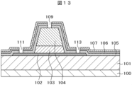
- 酸化物半導体によるTFTを有するTFT回路基板であって、
前記TFTは、酸化物半導体を覆ってゲート絶縁膜が形成され、前記ゲート絶縁膜の上にゲート電極が形成され、
前記酸化物半導体の前記ゲート電極で覆われた部分と前記ゲート電極で覆われていない部分は層間絶縁膜で覆われ、前記層間絶縁膜は硬化膜で覆われ、前記硬化膜は第1のAlO膜で覆われており、
前記層間絶縁膜と前記硬化膜と前記第1のAlO膜とを貫通してスルーホールが形成され、
ソース配線又はドレイン配線は前記スルーホールを介して前記酸化物半導体層のソース又はドレインと接続し、
前記層間絶縁膜の厚さは100乃至500nmであり、前記硬化膜の厚さは10乃至100nmであり、第1のAlO膜の厚さは10乃至100nmであることを特徴とするTFT回路基板。 - 前記ゲート絶縁膜は前記酸化物半導体の前記ゲート電極に対向する側の一部に形成されていることを特徴とする請求項1に記載のTFT回路基板。
- 前記層間絶縁膜と前記酸化物半導体あるいは前記ゲート電極の間には第2のAlO膜が形成されていることを特徴とする請求項1に記載のTFT回路基板。
Priority Applications (1)
| Application Number | Priority Date | Filing Date | Title |
|---|---|---|---|
| JP2022000800A JP7350903B2 (ja) | 2016-07-19 | 2022-01-06 | Tft回路基板 |
Applications Claiming Priority (2)
| Application Number | Priority Date | Filing Date | Title |
|---|---|---|---|
| JP2016141228A JP7007080B2 (ja) | 2016-07-19 | 2016-07-19 | Tft回路基板 |
| JP2022000800A JP7350903B2 (ja) | 2016-07-19 | 2022-01-06 | Tft回路基板 |
Related Parent Applications (1)
| Application Number | Title | Priority Date | Filing Date |
|---|---|---|---|
| JP2016141228A Division JP7007080B2 (ja) | 2016-07-19 | 2016-07-19 | Tft回路基板 |
Publications (2)
| Publication Number | Publication Date |
|---|---|
| JP2022058505A JP2022058505A (ja) | 2022-04-12 |
| JP7350903B2 true JP7350903B2 (ja) | 2023-09-26 |
Family
ID=60988124
Family Applications (2)
| Application Number | Title | Priority Date | Filing Date |
|---|---|---|---|
| JP2016141228A Active JP7007080B2 (ja) | 2016-07-19 | 2016-07-19 | Tft回路基板 |
| JP2022000800A Active JP7350903B2 (ja) | 2016-07-19 | 2022-01-06 | Tft回路基板 |
Family Applications Before (1)
| Application Number | Title | Priority Date | Filing Date |
|---|---|---|---|
| JP2016141228A Active JP7007080B2 (ja) | 2016-07-19 | 2016-07-19 | Tft回路基板 |
Country Status (2)
| Country | Link |
|---|---|
| US (3) | US11063154B2 (ja) |
| JP (2) | JP7007080B2 (ja) |
Families Citing this family (6)
| Publication number | Priority date | Publication date | Assignee | Title |
|---|---|---|---|---|
| JP7007080B2 (ja) * | 2016-07-19 | 2022-02-10 | 株式会社ジャパンディスプレイ | Tft回路基板 |
| CN107731929B (zh) * | 2017-09-28 | 2019-12-13 | 信利(惠州)智能显示有限公司 | 薄膜晶体管的制作方法 |
| WO2019150814A1 (ja) | 2018-01-30 | 2019-08-08 | 京セラ株式会社 | 電力管理サーバ及び電力管理方法 |
| KR20230164225A (ko) * | 2018-02-01 | 2023-12-01 | 가부시키가이샤 한도오따이 에네루기 켄큐쇼 | 표시 장치 및 전자 기기 |
| KR20220006686A (ko) | 2020-07-08 | 2022-01-18 | 삼성디스플레이 주식회사 | 표시 장치 및 그 제조 방법 |
| US11710657B2 (en) * | 2020-09-29 | 2023-07-25 | Taiwan Semiconductor Manufacturing Co., Ltd. | Middle-of-line interconnect structure having air gap and method of fabrication thereof |
Citations (5)
| Publication number | Priority date | Publication date | Assignee | Title |
|---|---|---|---|---|
| JP2012015436A (ja) | 2010-07-05 | 2012-01-19 | Sony Corp | 薄膜トランジスタおよび表示装置 |
| JP2013038404A (ja) | 2011-07-08 | 2013-02-21 | Semiconductor Energy Lab Co Ltd | 半導体装置及び半導体装置の作製方法 |
| JP2013211544A (ja) | 2012-03-02 | 2013-10-10 | Semiconductor Energy Lab Co Ltd | 半導体装置及び半導体装置の作製方法、並びに酸化膜の作製方法 |
| WO2014171056A1 (ja) | 2013-04-19 | 2014-10-23 | パナソニック株式会社 | 薄膜半導体装置、有機el表示装置、及びそれらの製造方法 |
| JP2017168642A (ja) | 2016-03-16 | 2017-09-21 | 株式会社Joled | 薄膜トランジスタ、及び薄膜トランジスタを備えた表示装置 |
Family Cites Families (23)
| Publication number | Priority date | Publication date | Assignee | Title |
|---|---|---|---|---|
| JP2007173488A (ja) | 2005-12-21 | 2007-07-05 | Toshiba Matsushita Display Technology Co Ltd | 薄膜トランジスタおよびその評価方法 |
| TWI389211B (zh) * | 2008-04-30 | 2013-03-11 | Chimei Innolux Corp | 影像顯示系統及其製造方法 |
| JP5584960B2 (ja) | 2008-07-03 | 2014-09-10 | ソニー株式会社 | 薄膜トランジスタおよび表示装置 |
| US8294159B2 (en) * | 2009-10-12 | 2012-10-23 | Monolithic 3D Inc. | Method for fabrication of a semiconductor device and structure |
| WO2011074407A1 (en) * | 2009-12-18 | 2011-06-23 | Semiconductor Energy Laboratory Co., Ltd. | Semiconductor device and method for manufacturing the same |
| US8298875B1 (en) * | 2011-03-06 | 2012-10-30 | Monolithic 3D Inc. | Method for fabrication of a semiconductor device and structure |
| JP5708910B2 (ja) * | 2010-03-30 | 2015-04-30 | ソニー株式会社 | 薄膜トランジスタおよびその製造方法、並びに表示装置 |
| US9082860B2 (en) * | 2011-03-31 | 2015-07-14 | Semiconductor Energy Laboratory Co., Ltd. | Semiconductor device |
| WO2013094547A1 (en) | 2011-12-23 | 2013-06-27 | Semiconductor Energy Laboratory Co., Ltd. | Semiconductor device and method for manufacturing the same |
| US8969867B2 (en) | 2012-01-18 | 2015-03-03 | Semiconductor Energy Laboratory Co., Ltd. | Semiconductor device |
| JP6004420B2 (ja) | 2012-03-14 | 2016-10-05 | 国立研究開発法人産業技術総合研究所 | 不揮発性化合物の除去方法 |
| US8987047B2 (en) | 2012-04-02 | 2015-03-24 | Samsung Display Co., Ltd. | Thin film transistor, thin film transistor array panel including the same, and method of manufacturing the same |
| US9276121B2 (en) | 2012-04-12 | 2016-03-01 | Semiconductor Energy Laboratory Co., Ltd. | Semiconductor device and method for manufacturing the same |
| US9929276B2 (en) * | 2012-08-10 | 2018-03-27 | Semiconductor Energy Laboratory Co., Ltd. | Semiconductor device and method for manufacturing the same |
| JP6108898B2 (ja) * | 2013-03-19 | 2017-04-05 | 株式会社東芝 | 表示装置、薄膜トランジスタ、表示装置の製造方法及び薄膜トランジスタの製造方法 |
| KR20150053314A (ko) * | 2013-11-07 | 2015-05-18 | 삼성디스플레이 주식회사 | 박막 트랜지스터 및 이를 포함하는 표시장치 |
| JP2015198223A (ja) | 2014-04-03 | 2015-11-09 | 株式会社ジャパンディスプレイ | 表示装置およびその製造方法 |
| JP6311899B2 (ja) * | 2014-05-09 | 2018-04-18 | 株式会社Joled | 薄膜トランジスタ基板及びその製造方法 |
| JP2016111105A (ja) * | 2014-12-03 | 2016-06-20 | 株式会社Joled | 薄膜トランジスタ及びその製造方法、並びに、表示装置 |
| JP6519073B2 (ja) * | 2014-12-03 | 2019-05-29 | 株式会社Joled | 薄膜トランジスタ及びその製造方法、並びに、表示装置 |
| JP2017175022A (ja) * | 2016-03-24 | 2017-09-28 | 株式会社Joled | 薄膜トランジスタ |
| JP7007080B2 (ja) * | 2016-07-19 | 2022-02-10 | 株式会社ジャパンディスプレイ | Tft回路基板 |
| JP2018170326A (ja) * | 2017-03-29 | 2018-11-01 | 株式会社ジャパンディスプレイ | 表示装置 |
-
2016
- 2016-07-19 JP JP2016141228A patent/JP7007080B2/ja active Active
-
2017
- 2017-07-13 US US15/649,126 patent/US11063154B2/en active Active
-
2021
- 2021-06-15 US US17/347,630 patent/US11742430B2/en active Active
-
2022
- 2022-01-06 JP JP2022000800A patent/JP7350903B2/ja active Active
-
2023
- 2023-07-05 US US18/346,927 patent/US20230361220A1/en active Pending
Patent Citations (5)
| Publication number | Priority date | Publication date | Assignee | Title |
|---|---|---|---|---|
| JP2012015436A (ja) | 2010-07-05 | 2012-01-19 | Sony Corp | 薄膜トランジスタおよび表示装置 |
| JP2013038404A (ja) | 2011-07-08 | 2013-02-21 | Semiconductor Energy Lab Co Ltd | 半導体装置及び半導体装置の作製方法 |
| JP2013211544A (ja) | 2012-03-02 | 2013-10-10 | Semiconductor Energy Lab Co Ltd | 半導体装置及び半導体装置の作製方法、並びに酸化膜の作製方法 |
| WO2014171056A1 (ja) | 2013-04-19 | 2014-10-23 | パナソニック株式会社 | 薄膜半導体装置、有機el表示装置、及びそれらの製造方法 |
| JP2017168642A (ja) | 2016-03-16 | 2017-09-21 | 株式会社Joled | 薄膜トランジスタ、及び薄膜トランジスタを備えた表示装置 |
Also Published As
| Publication number | Publication date |
|---|---|
| US20230361220A1 (en) | 2023-11-09 |
| JP2018013525A (ja) | 2018-01-25 |
| JP2022058505A (ja) | 2022-04-12 |
| US20210305434A1 (en) | 2021-09-30 |
| US20180026138A1 (en) | 2018-01-25 |
| US11063154B2 (en) | 2021-07-13 |
| US11742430B2 (en) | 2023-08-29 |
| JP7007080B2 (ja) | 2022-02-10 |
Similar Documents
| Publication | Publication Date | Title |
|---|---|---|
| JP7350903B2 (ja) | Tft回路基板 | |
| US10317763B2 (en) | Display device | |
| US20180286888A1 (en) | Display device | |
| US11855102B2 (en) | Display device | |
| KR102380647B1 (ko) | 박막 트랜지스터 및 그 제조 방법 | |
| JP2009211009A (ja) | 液晶表示装置 | |
| WO2012132953A1 (ja) | 表示装置 | |
| JP2018170326A (ja) | 表示装置 | |
| JP2013055080A (ja) | 表示装置および表示装置の製造方法 | |
| US10340392B2 (en) | Semiconductor device including mark portion and production method for same | |
| US11309336B2 (en) | Display device | |
| US11374025B2 (en) | Display device and manufacturing method thereof | |
| US10707240B2 (en) | Display device | |
| JP2019186301A (ja) | 表示装置及びその製造方法 | |
| JP7446076B2 (ja) | 半導体装置 | |
| JP2016139142A (ja) | 表示装置および表示装置の製造方法 | |
| KR20150111550A (ko) | 박막 트랜지스터 표시판 및 그 제조 방법 | |
| JP2019016640A (ja) | 表示装置 |
Legal Events
| Date | Code | Title | Description |
|---|---|---|---|
| A621 | Written request for application examination |
Free format text: JAPANESE INTERMEDIATE CODE: A621 Effective date: 20220106 |
|
| A977 | Report on retrieval |
Free format text: JAPANESE INTERMEDIATE CODE: A971007 Effective date: 20230228 |
|
| A131 | Notification of reasons for refusal |
Free format text: JAPANESE INTERMEDIATE CODE: A131 Effective date: 20230307 |
|
| A521 | Request for written amendment filed |
Free format text: JAPANESE INTERMEDIATE CODE: A523 Effective date: 20230428 |
|
| TRDD | Decision of grant or rejection written | ||
| A01 | Written decision to grant a patent or to grant a registration (utility model) |
Free format text: JAPANESE INTERMEDIATE CODE: A01 Effective date: 20230815 |
|
| A61 | First payment of annual fees (during grant procedure) |
Free format text: JAPANESE INTERMEDIATE CODE: A61 Effective date: 20230913 |
|
| R150 | Certificate of patent or registration of utility model |
Ref document number: 7350903 Country of ref document: JP Free format text: JAPANESE INTERMEDIATE CODE: R150 |