JP6519073B2 - 薄膜トランジスタ及びその製造方法、並びに、表示装置 - Google Patents
薄膜トランジスタ及びその製造方法、並びに、表示装置 Download PDFInfo
- Publication number
- JP6519073B2 JP6519073B2 JP2014245398A JP2014245398A JP6519073B2 JP 6519073 B2 JP6519073 B2 JP 6519073B2 JP 2014245398 A JP2014245398 A JP 2014245398A JP 2014245398 A JP2014245398 A JP 2014245398A JP 6519073 B2 JP6519073 B2 JP 6519073B2
- Authority
- JP
- Japan
- Prior art keywords
- layer
- metal
- oxide semiconductor
- semiconductor layer
- metal oxide
- Prior art date
- Legal status (The legal status is an assumption and is not a legal conclusion. Google has not performed a legal analysis and makes no representation as to the accuracy of the status listed.)
- Active
Links
- 239000010409 thin film Substances 0.000 title claims description 91
- 238000000034 method Methods 0.000 title claims description 25
- 238000004519 manufacturing process Methods 0.000 title claims description 22
- 239000010408 film Substances 0.000 claims description 161
- 239000004065 semiconductor Substances 0.000 claims description 158
- 229910044991 metal oxide Inorganic materials 0.000 claims description 130
- 150000004706 metal oxides Chemical class 0.000 claims description 130
- 239000000758 substrate Substances 0.000 claims description 89
- 229910052751 metal Inorganic materials 0.000 claims description 77
- 239000002184 metal Substances 0.000 claims description 77
- QVGXLLKOCUKJST-UHFFFAOYSA-N atomic oxygen Chemical compound [O] QVGXLLKOCUKJST-UHFFFAOYSA-N 0.000 claims description 66
- 239000001301 oxygen Substances 0.000 claims description 66
- 229910052760 oxygen Inorganic materials 0.000 claims description 66
- 238000005546 reactive sputtering Methods 0.000 claims description 27
- 238000010494 dissociation reaction Methods 0.000 claims description 24
- 230000005593 dissociations Effects 0.000 claims description 24
- XAGFODPZIPBFFR-UHFFFAOYSA-N aluminium Chemical compound [Al] XAGFODPZIPBFFR-UHFFFAOYSA-N 0.000 claims description 20
- 229910052782 aluminium Inorganic materials 0.000 claims description 19
- 229910052738 indium Inorganic materials 0.000 claims description 12
- 238000010438 heat treatment Methods 0.000 claims description 11
- APFVFJFRJDLVQX-UHFFFAOYSA-N indium atom Chemical compound [In] APFVFJFRJDLVQX-UHFFFAOYSA-N 0.000 claims description 9
- 229910052733 gallium Inorganic materials 0.000 claims description 7
- 239000011701 zinc Substances 0.000 claims description 6
- 229910052725 zinc Inorganic materials 0.000 claims description 5
- GYHNNYVSQQEPJS-UHFFFAOYSA-N Gallium Chemical compound [Ga] GYHNNYVSQQEPJS-UHFFFAOYSA-N 0.000 claims description 4
- HCHKCACWOHOZIP-UHFFFAOYSA-N Zinc Chemical compound [Zn] HCHKCACWOHOZIP-UHFFFAOYSA-N 0.000 claims description 2
- 239000010410 layer Substances 0.000 description 416
- 238000005401 electroluminescence Methods 0.000 description 34
- 239000011229 interlayer Substances 0.000 description 24
- 239000000463 material Substances 0.000 description 17
- 238000004544 sputter deposition Methods 0.000 description 14
- 239000007789 gas Substances 0.000 description 12
- XUIMIQQOPSSXEZ-UHFFFAOYSA-N Silicon Chemical compound [Si] XUIMIQQOPSSXEZ-UHFFFAOYSA-N 0.000 description 11
- 229910052710 silicon Inorganic materials 0.000 description 11
- 239000010703 silicon Substances 0.000 description 11
- 238000010586 diagram Methods 0.000 description 9
- 238000009826 distribution Methods 0.000 description 9
- 229910052814 silicon oxide Inorganic materials 0.000 description 9
- 238000012360 testing method Methods 0.000 description 9
- 239000010936 titanium Substances 0.000 description 9
- VYPSYNLAJGMNEJ-UHFFFAOYSA-N Silicium dioxide Chemical compound O=[Si]=O VYPSYNLAJGMNEJ-UHFFFAOYSA-N 0.000 description 8
- 238000000137 annealing Methods 0.000 description 8
- 239000003990 capacitor Substances 0.000 description 8
- 238000005530 etching Methods 0.000 description 8
- 239000011521 glass Substances 0.000 description 8
- 230000003071 parasitic effect Effects 0.000 description 8
- LIVNPJMFVYWSIS-UHFFFAOYSA-N silicon monoxide Chemical compound [Si-]#[O+] LIVNPJMFVYWSIS-UHFFFAOYSA-N 0.000 description 8
- 239000002356 single layer Substances 0.000 description 8
- 229910007541 Zn O Inorganic materials 0.000 description 7
- 230000015572 biosynthetic process Effects 0.000 description 7
- TWNQGVIAIRXVLR-UHFFFAOYSA-N oxo(oxoalumanyloxy)alumane Chemical compound O=[Al]O[Al]=O TWNQGVIAIRXVLR-UHFFFAOYSA-N 0.000 description 7
- QTBSBXVTEAMEQO-UHFFFAOYSA-N Acetic acid Chemical compound CC(O)=O QTBSBXVTEAMEQO-UHFFFAOYSA-N 0.000 description 6
- ZOKXTWBITQBERF-UHFFFAOYSA-N Molybdenum Chemical compound [Mo] ZOKXTWBITQBERF-UHFFFAOYSA-N 0.000 description 6
- 229910052750 molybdenum Inorganic materials 0.000 description 6
- 239000011733 molybdenum Substances 0.000 description 6
- 238000001039 wet etching Methods 0.000 description 6
- RTAQQCXQSZGOHL-UHFFFAOYSA-N Titanium Chemical compound [Ti] RTAQQCXQSZGOHL-UHFFFAOYSA-N 0.000 description 5
- 238000004833 X-ray photoelectron spectroscopy Methods 0.000 description 5
- 239000010949 copper Substances 0.000 description 5
- 229910052719 titanium Inorganic materials 0.000 description 5
- WFKWXMTUELFFGS-UHFFFAOYSA-N tungsten Chemical compound [W] WFKWXMTUELFFGS-UHFFFAOYSA-N 0.000 description 5
- 229910052721 tungsten Inorganic materials 0.000 description 5
- 239000010937 tungsten Substances 0.000 description 5
- NBIIXXVUZAFLBC-UHFFFAOYSA-N Phosphoric acid Chemical compound OP(O)(O)=O NBIIXXVUZAFLBC-UHFFFAOYSA-N 0.000 description 4
- XLOMVQKBTHCTTD-UHFFFAOYSA-N Zinc monoxide Chemical compound [Zn]=O XLOMVQKBTHCTTD-UHFFFAOYSA-N 0.000 description 4
- 238000005229 chemical vapour deposition Methods 0.000 description 4
- 239000011651 chromium Substances 0.000 description 4
- 238000000151 deposition Methods 0.000 description 4
- 238000001312 dry etching Methods 0.000 description 4
- 238000002347 injection Methods 0.000 description 4
- 239000007924 injection Substances 0.000 description 4
- 239000000203 mixture Substances 0.000 description 4
- 238000000206 photolithography Methods 0.000 description 4
- -1 polyethylene Polymers 0.000 description 4
- 230000009467 reduction Effects 0.000 description 4
- 239000000126 substance Substances 0.000 description 4
- WGTYBPLFGIVFAS-UHFFFAOYSA-M tetramethylammonium hydroxide Chemical compound [OH-].C[N+](C)(C)C WGTYBPLFGIVFAS-UHFFFAOYSA-M 0.000 description 4
- RYGMFSIKBFXOCR-UHFFFAOYSA-N Copper Chemical compound [Cu] RYGMFSIKBFXOCR-UHFFFAOYSA-N 0.000 description 3
- KRHYYFGTRYWZRS-UHFFFAOYSA-N Fluorane Chemical compound F KRHYYFGTRYWZRS-UHFFFAOYSA-N 0.000 description 3
- 239000004642 Polyimide Substances 0.000 description 3
- 229910052581 Si3N4 Inorganic materials 0.000 description 3
- 239000000956 alloy Substances 0.000 description 3
- 229910045601 alloy Inorganic materials 0.000 description 3
- 239000004020 conductor Substances 0.000 description 3
- 229910052802 copper Inorganic materials 0.000 description 3
- 230000008021 deposition Effects 0.000 description 3
- 239000011159 matrix material Substances 0.000 description 3
- 230000000704 physical effect Effects 0.000 description 3
- 238000001020 plasma etching Methods 0.000 description 3
- 229920001721 polyimide Polymers 0.000 description 3
- 230000008569 process Effects 0.000 description 3
- HQVNEWCFYHHQES-UHFFFAOYSA-N silicon nitride Chemical compound N12[Si]34N5[Si]62N3[Si]51N64 HQVNEWCFYHHQES-UHFFFAOYSA-N 0.000 description 3
- 239000000243 solution Substances 0.000 description 3
- TVIVIEFSHFOWTE-UHFFFAOYSA-K tri(quinolin-8-yloxy)alumane Chemical compound [Al+3].C1=CN=C2C([O-])=CC=CC2=C1.C1=CN=C2C([O-])=CC=CC2=C1.C1=CN=C2C([O-])=CC=CC2=C1 TVIVIEFSHFOWTE-UHFFFAOYSA-K 0.000 description 3
- XKRFYHLGVUSROY-UHFFFAOYSA-N Argon Chemical compound [Ar] XKRFYHLGVUSROY-UHFFFAOYSA-N 0.000 description 2
- VYZAMTAEIAYCRO-UHFFFAOYSA-N Chromium Chemical compound [Cr] VYZAMTAEIAYCRO-UHFFFAOYSA-N 0.000 description 2
- MYMOFIZGZYHOMD-UHFFFAOYSA-N Dioxygen Chemical compound O=O MYMOFIZGZYHOMD-UHFFFAOYSA-N 0.000 description 2
- 206010021143 Hypoxia Diseases 0.000 description 2
- GRYLNZFGIOXLOG-UHFFFAOYSA-N Nitric acid Chemical compound O[N+]([O-])=O GRYLNZFGIOXLOG-UHFFFAOYSA-N 0.000 description 2
- GQPLMRYTRLFLPF-UHFFFAOYSA-N Nitrous Oxide Chemical compound [O-][N+]#N GQPLMRYTRLFLPF-UHFFFAOYSA-N 0.000 description 2
- 229910018503 SF6 Inorganic materials 0.000 description 2
- 238000000560 X-ray reflectometry Methods 0.000 description 2
- 239000003513 alkali Substances 0.000 description 2
- 229910000147 aluminium phosphate Inorganic materials 0.000 description 2
- 238000000231 atomic layer deposition Methods 0.000 description 2
- 239000000460 chlorine Substances 0.000 description 2
- 229910052804 chromium Inorganic materials 0.000 description 2
- 238000011161 development Methods 0.000 description 2
- 229910001882 dioxygen Inorganic materials 0.000 description 2
- 230000005525 hole transport Effects 0.000 description 2
- 238000003384 imaging method Methods 0.000 description 2
- 238000010030 laminating Methods 0.000 description 2
- 239000004973 liquid crystal related substance Substances 0.000 description 2
- 238000012986 modification Methods 0.000 description 2
- 230000004048 modification Effects 0.000 description 2
- MGRWKWACZDFZJT-UHFFFAOYSA-N molybdenum tungsten Chemical compound [Mo].[W] MGRWKWACZDFZJT-UHFFFAOYSA-N 0.000 description 2
- 125000000896 monocarboxylic acid group Chemical group 0.000 description 2
- 229910017604 nitric acid Inorganic materials 0.000 description 2
- 150000004767 nitrides Chemical class 0.000 description 2
- 230000003647 oxidation Effects 0.000 description 2
- 238000007254 oxidation reaction Methods 0.000 description 2
- 230000001590 oxidative effect Effects 0.000 description 2
- 238000012545 processing Methods 0.000 description 2
- 230000001737 promoting effect Effects 0.000 description 2
- 239000011347 resin Substances 0.000 description 2
- 229920005989 resin Polymers 0.000 description 2
- SFZCNBIFKDRMGX-UHFFFAOYSA-N sulfur hexafluoride Chemical compound FS(F)(F)(F)(F)F SFZCNBIFKDRMGX-UHFFFAOYSA-N 0.000 description 2
- 229960000909 sulfur hexafluoride Drugs 0.000 description 2
- 239000013077 target material Substances 0.000 description 2
- JBQYATWDVHIOAR-UHFFFAOYSA-N tellanylidenegermanium Chemical compound [Te]=[Ge] JBQYATWDVHIOAR-UHFFFAOYSA-N 0.000 description 2
- XLYOFNOQVPJJNP-UHFFFAOYSA-N water Substances O XLYOFNOQVPJJNP-UHFFFAOYSA-N 0.000 description 2
- 239000011787 zinc oxide Substances 0.000 description 2
- 125000001637 1-naphthyl group Chemical group [H]C1=C([H])C([H])=C2C(*)=C([H])C([H])=C([H])C2=C1[H] 0.000 description 1
- ZAMOUSCENKQFHK-UHFFFAOYSA-N Chlorine atom Chemical compound [Cl] ZAMOUSCENKQFHK-UHFFFAOYSA-N 0.000 description 1
- DGAQECJNVWCQMB-PUAWFVPOSA-M Ilexoside XXIX Chemical compound C[C@@H]1CC[C@@]2(CC[C@@]3(C(=CC[C@H]4[C@]3(CC[C@@H]5[C@@]4(CC[C@@H](C5(C)C)OS(=O)(=O)[O-])C)C)[C@@H]2[C@]1(C)O)C)C(=O)O[C@H]6[C@@H]([C@H]([C@@H]([C@H](O6)CO)O)O)O.[Na+] DGAQECJNVWCQMB-PUAWFVPOSA-M 0.000 description 1
- 229920000144 PEDOT:PSS Polymers 0.000 description 1
- OAICVXFJPJFONN-UHFFFAOYSA-N Phosphorus Chemical compound [P] OAICVXFJPJFONN-UHFFFAOYSA-N 0.000 description 1
- 239000004698 Polyethylene Substances 0.000 description 1
- 239000004743 Polypropylene Substances 0.000 description 1
- BLRPTPMANUNPDV-UHFFFAOYSA-N Silane Chemical compound [SiH4] BLRPTPMANUNPDV-UHFFFAOYSA-N 0.000 description 1
- BQCADISMDOOEFD-UHFFFAOYSA-N Silver Chemical compound [Ag] BQCADISMDOOEFD-UHFFFAOYSA-N 0.000 description 1
- 229910006404 SnO 2 Inorganic materials 0.000 description 1
- 238000007792 addition Methods 0.000 description 1
- 239000012670 alkaline solution Substances 0.000 description 1
- 238000004458 analytical method Methods 0.000 description 1
- 239000007864 aqueous solution Substances 0.000 description 1
- 229910052786 argon Inorganic materials 0.000 description 1
- HFACYLZERDEVSX-UHFFFAOYSA-N benzidine Chemical compound C1=CC(N)=CC=C1C1=CC=C(N)C=C1 HFACYLZERDEVSX-UHFFFAOYSA-N 0.000 description 1
- 230000008859 change Effects 0.000 description 1
- 229910052801 chlorine Inorganic materials 0.000 description 1
- 238000005520 cutting process Methods 0.000 description 1
- 230000007547 defect Effects 0.000 description 1
- 238000006073 displacement reaction Methods 0.000 description 1
- 230000000694 effects Effects 0.000 description 1
- 238000010292 electrical insulation Methods 0.000 description 1
- 238000005566 electron beam evaporation Methods 0.000 description 1
- 239000000284 extract Substances 0.000 description 1
- PCHJSUWPFVWCPO-UHFFFAOYSA-N gold Chemical compound [Au] PCHJSUWPFVWCPO-UHFFFAOYSA-N 0.000 description 1
- 229910052737 gold Inorganic materials 0.000 description 1
- 239000010931 gold Substances 0.000 description 1
- RBTKNAXYKSUFRK-UHFFFAOYSA-N heliogen blue Chemical compound [Cu].[N-]1C2=C(C=CC=C3)C3=C1N=C([N-]1)C3=CC=CC=C3C1=NC([N-]1)=C(C=CC=C3)C3=C1N=C([N-]1)C3=CC=CC=C3C1=N2 RBTKNAXYKSUFRK-UHFFFAOYSA-N 0.000 description 1
- 239000012535 impurity Substances 0.000 description 1
- 229910003437 indium oxide Inorganic materials 0.000 description 1
- PJXISJQVUVHSOJ-UHFFFAOYSA-N indium(iii) oxide Chemical compound [O-2].[O-2].[O-2].[In+3].[In+3] PJXISJQVUVHSOJ-UHFFFAOYSA-N 0.000 description 1
- 239000011261 inert gas Substances 0.000 description 1
- 238000011835 investigation Methods 0.000 description 1
- 238000000608 laser ablation Methods 0.000 description 1
- 239000002346 layers by function Substances 0.000 description 1
- 239000007769 metal material Substances 0.000 description 1
- QPJSUIGXIBEQAC-UHFFFAOYSA-N n-(2,4-dichloro-5-propan-2-yloxyphenyl)acetamide Chemical compound CC(C)OC1=CC(NC(C)=O)=C(Cl)C=C1Cl QPJSUIGXIBEQAC-UHFFFAOYSA-N 0.000 description 1
- IBHBKWKFFTZAHE-UHFFFAOYSA-N n-[4-[4-(n-naphthalen-1-ylanilino)phenyl]phenyl]-n-phenylnaphthalen-1-amine Chemical compound C1=CC=CC=C1N(C=1C2=CC=CC=C2C=CC=1)C1=CC=C(C=2C=CC(=CC=2)N(C=2C=CC=CC=2)C=2C3=CC=CC=C3C=CC=2)C=C1 IBHBKWKFFTZAHE-UHFFFAOYSA-N 0.000 description 1
- 239000001272 nitrous oxide Substances 0.000 description 1
- 239000011368 organic material Substances 0.000 description 1
- 150000007978 oxazole derivatives Chemical class 0.000 description 1
- BPUBBGLMJRNUCC-UHFFFAOYSA-N oxygen(2-);tantalum(5+) Chemical compound [O-2].[O-2].[O-2].[O-2].[O-2].[Ta+5].[Ta+5] BPUBBGLMJRNUCC-UHFFFAOYSA-N 0.000 description 1
- 229910052698 phosphorus Inorganic materials 0.000 description 1
- 239000011574 phosphorus Substances 0.000 description 1
- 238000005268 plasma chemical vapour deposition Methods 0.000 description 1
- 229920003207 poly(ethylene-2,6-naphthalate) Polymers 0.000 description 1
- 229920000573 polyethylene Polymers 0.000 description 1
- 239000011112 polyethylene naphthalate Substances 0.000 description 1
- 229920000139 polyethylene terephthalate Polymers 0.000 description 1
- 239000005020 polyethylene terephthalate Substances 0.000 description 1
- 229920001155 polypropylene Polymers 0.000 description 1
- 238000002360 preparation method Methods 0.000 description 1
- 239000010453 quartz Substances 0.000 description 1
- 238000001552 radio frequency sputter deposition Methods 0.000 description 1
- 229910000077 silane Inorganic materials 0.000 description 1
- 229910052709 silver Inorganic materials 0.000 description 1
- 239000004332 silver Substances 0.000 description 1
- 239000011734 sodium Substances 0.000 description 1
- 229910052708 sodium Inorganic materials 0.000 description 1
- 229910001936 tantalum oxide Inorganic materials 0.000 description 1
- TXEYQDLBPFQVAA-UHFFFAOYSA-N tetrafluoromethane Chemical compound FC(F)(F)F TXEYQDLBPFQVAA-UHFFFAOYSA-N 0.000 description 1
- FAQYAMRNWDIXMY-UHFFFAOYSA-N trichloroborane Chemical compound ClB(Cl)Cl FAQYAMRNWDIXMY-UHFFFAOYSA-N 0.000 description 1
- 238000001771 vacuum deposition Methods 0.000 description 1
Images


Classifications
-
- H—ELECTRICITY
- H01—ELECTRIC ELEMENTS
- H01L—SEMICONDUCTOR DEVICES NOT COVERED BY CLASS H10
- H01L29/00—Semiconductor devices adapted for rectifying, amplifying, oscillating or switching, or capacitors or resistors with at least one potential-jump barrier or surface barrier, e.g. PN junction depletion layer or carrier concentration layer; Details of semiconductor bodies or of electrodes thereof ; Multistep manufacturing processes therefor
- H01L29/66—Types of semiconductor device ; Multistep manufacturing processes therefor
- H01L29/68—Types of semiconductor device ; Multistep manufacturing processes therefor controllable by only the electric current supplied, or only the electric potential applied, to an electrode which does not carry the current to be rectified, amplified or switched
- H01L29/76—Unipolar devices, e.g. field effect transistors
- H01L29/772—Field effect transistors
- H01L29/78—Field effect transistors with field effect produced by an insulated gate
- H01L29/786—Thin film transistors, i.e. transistors with a channel being at least partly a thin film
- H01L29/7869—Thin film transistors, i.e. transistors with a channel being at least partly a thin film having a semiconductor body comprising an oxide semiconductor material, e.g. zinc oxide, copper aluminium oxide, cadmium stannate
-
- H—ELECTRICITY
- H01—ELECTRIC ELEMENTS
- H01L—SEMICONDUCTOR DEVICES NOT COVERED BY CLASS H10
- H01L29/00—Semiconductor devices adapted for rectifying, amplifying, oscillating or switching, or capacitors or resistors with at least one potential-jump barrier or surface barrier, e.g. PN junction depletion layer or carrier concentration layer; Details of semiconductor bodies or of electrodes thereof ; Multistep manufacturing processes therefor
- H01L29/40—Electrodes ; Multistep manufacturing processes therefor
- H01L29/43—Electrodes ; Multistep manufacturing processes therefor characterised by the materials of which they are formed
- H01L29/45—Ohmic electrodes
-
- H—ELECTRICITY
- H01—ELECTRIC ELEMENTS
- H01L—SEMICONDUCTOR DEVICES NOT COVERED BY CLASS H10
- H01L29/00—Semiconductor devices adapted for rectifying, amplifying, oscillating or switching, or capacitors or resistors with at least one potential-jump barrier or surface barrier, e.g. PN junction depletion layer or carrier concentration layer; Details of semiconductor bodies or of electrodes thereof ; Multistep manufacturing processes therefor
- H01L29/66—Types of semiconductor device ; Multistep manufacturing processes therefor
- H01L29/66007—Multistep manufacturing processes
- H01L29/66969—Multistep manufacturing processes of devices having semiconductor bodies not comprising group 14 or group 13/15 materials
-
- H—ELECTRICITY
- H01—ELECTRIC ELEMENTS
- H01L—SEMICONDUCTOR DEVICES NOT COVERED BY CLASS H10
- H01L29/00—Semiconductor devices adapted for rectifying, amplifying, oscillating or switching, or capacitors or resistors with at least one potential-jump barrier or surface barrier, e.g. PN junction depletion layer or carrier concentration layer; Details of semiconductor bodies or of electrodes thereof ; Multistep manufacturing processes therefor
- H01L29/66—Types of semiconductor device ; Multistep manufacturing processes therefor
- H01L29/68—Types of semiconductor device ; Multistep manufacturing processes therefor controllable by only the electric current supplied, or only the electric potential applied, to an electrode which does not carry the current to be rectified, amplified or switched
- H01L29/76—Unipolar devices, e.g. field effect transistors
- H01L29/772—Field effect transistors
- H01L29/78—Field effect transistors with field effect produced by an insulated gate
- H01L29/786—Thin film transistors, i.e. transistors with a channel being at least partly a thin film
- H01L29/78606—Thin film transistors, i.e. transistors with a channel being at least partly a thin film with supplementary region or layer in the thin film or in the insulated bulk substrate supporting it for controlling or increasing the safety of the device
- H01L29/78618—Thin film transistors, i.e. transistors with a channel being at least partly a thin film with supplementary region or layer in the thin film or in the insulated bulk substrate supporting it for controlling or increasing the safety of the device characterised by the drain or the source properties, e.g. the doping structure, the composition, the sectional shape or the contact structure
-
- H—ELECTRICITY
- H01—ELECTRIC ELEMENTS
- H01L—SEMICONDUCTOR DEVICES NOT COVERED BY CLASS H10
- H01L29/00—Semiconductor devices adapted for rectifying, amplifying, oscillating or switching, or capacitors or resistors with at least one potential-jump barrier or surface barrier, e.g. PN junction depletion layer or carrier concentration layer; Details of semiconductor bodies or of electrodes thereof ; Multistep manufacturing processes therefor
- H01L29/66—Types of semiconductor device ; Multistep manufacturing processes therefor
- H01L29/68—Types of semiconductor device ; Multistep manufacturing processes therefor controllable by only the electric current supplied, or only the electric potential applied, to an electrode which does not carry the current to be rectified, amplified or switched
- H01L29/76—Unipolar devices, e.g. field effect transistors
- H01L29/772—Field effect transistors
- H01L29/78—Field effect transistors with field effect produced by an insulated gate
- H01L29/786—Thin film transistors, i.e. transistors with a channel being at least partly a thin film
- H01L29/7869—Thin film transistors, i.e. transistors with a channel being at least partly a thin film having a semiconductor body comprising an oxide semiconductor material, e.g. zinc oxide, copper aluminium oxide, cadmium stannate
- H01L29/78693—Thin film transistors, i.e. transistors with a channel being at least partly a thin film having a semiconductor body comprising an oxide semiconductor material, e.g. zinc oxide, copper aluminium oxide, cadmium stannate the semiconducting oxide being amorphous
Description
上記課題を解決するために、本発明の一態様に係る薄膜トランジスタは、チャネル領域、並びに、当該チャネル領域より抵抗率が低いソース領域及びドレイン領域を有する酸化物半導体層と、前記酸化物半導体層の上方に設けられたゲート絶縁層と、前記ゲート絶縁層の上方で、かつ、前記チャネル領域に対向する位置に設けられたゲート電極と、前記酸化物半導体層上に設けられ、かつ、前記ソース領域及び前記ドレイン領域に接触する金属酸化物層とを備え、前記金属酸化物層は、前記酸化物半導体層に含まれる第1金属より、酸素との結合解離エネルギーが高い第2金属の酸化物を主成分として含み、前記金属酸化物層と前記酸化物半導体層との界面層における前記第2金属に対する酸素の第1濃度比は、前記金属酸化物層のバルク層における前記第2金属に対する酸素の第2濃度比より大きい。
[1.有機EL表示装置]
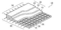
まず、本実施の形態に係る有機EL表示装置の概要について、図1〜図3を用いて説明する。なお、図1は、本実施の形態に係る薄膜半導体アレイ基板1の構成を示す図である。図2は、本実施の形態に係る有機EL表示装置10の一部切り欠き斜視図である。図3は、本実施の形態に係る有機EL表示装置10における画素回路31の回路構成を示す図である。
以下では、本実施の形態に係るTFT基板20に形成される薄膜トランジスタについて、図4A及び図4Bを用いて説明する。なお、図4Aは、本実施の形態に係る薄膜トランジスタ100の概略断面図である。図4Bは、本実施の形態に係る薄膜トランジスタ100の酸化物半導体層120と金属酸化物層150との界面層160を示す概略断面図である。
支持基板105は、例えば、電気絶縁性を有する材料から構成される基板である。例えば、支持基板105は、無アルカリガラス、石英ガラス、高耐熱性ガラスなどのガラス材料、又は、ポリエチレン、ポリプロピレン、ポリイミドなどの樹脂材料から構成される基板である。
フレキシブル基板110は、例えば、シート状又はフィルム状の可撓性を有する基板である。フレキシブル基板110は、例えば、ポリイミド、ポリエチレンテレフタレート、ポリエチレンナフタレートなどのフィルム材料の単層又は積層で構成された基板である。
アンダーコート層115は、フレキシブル基板110上に設けられた無機層の一例である。アンダーコート層115は、フレキシブル基板110の表面(酸化物半導体層120が形成される側の面)に形成されている。アンダーコート層115が設けられることにより、支持基板105(ガラス基板)又はフレキシブル基板110に含まれる不純物(例えば、ナトリウム及びリンなど)、又は、大気中の水分などが酸化物半導体層120に浸入するのを抑制することができる。これにより、酸化物半導体層120の膜質を安定化させて、TFT特性を安定化させることができる。
酸化物半導体層120は、チャネル層として用いられる。具体的には、図4Aに示すように、酸化物半導体層120は、チャネル領域121、ソース領域122及びドレイン領域123を有する。チャネル領域121は、ゲート絶縁層130を挟んでゲート電極140と対向する領域である。ソース領域122及びドレイン領域123は、チャネル領域121より抵抗率が低い低抵抗化領域(オフセット領域)である。ソース領域122及びドレイン領域123は、例えば、成膜した酸化物半導体の所定の領域に対して酸素欠損を引き起こすことで形成される。酸化物半導体層120の詳細な膜物性については、後で説明する。
ゲート絶縁層130は、酸化物半導体層120の上方に設けられている。具体的には、ゲート絶縁層130は、酸化物半導体層120とゲート電極140との間で、例えば、酸化物半導体層120上に設けられている。
ゲート電極140は、ゲート絶縁層130の上方で、かつ、チャネル領域121に対向する位置に設けられている。例えば、ゲート電極140は、ゲート絶縁層130上に所定形状で形成される。具体的には、ゲート電極140の側面は、ゲート絶縁層130の側面と面一であり、上面視において、ゲート電極140の輪郭線とゲート絶縁層130の輪郭線とは略一致している。
金属酸化物層150は、酸化物半導体層120上に設けられ、かつ、ソース領域122及びドレイン領域123に接触している。本実施の形態では、金属酸化物層150は、酸化物半導体層120の上面のうち、ゲート絶縁層130によって覆われていない部分に設けられている。具体的には、金属酸化物層150は、ソース領域122上及びドレイン領域123上に設けられている。
界面層160は、酸化物半導体層120と金属酸化物層150との界面に形成される層である。具体的には、界面層160は、金属酸化物層150が酸化物半導体層120上に積層されることによって形成される。より具体的には、界面層160は、金属酸化物層150が酸化物半導体層120に接触して、酸化物半導体層120の酸素が金属酸化物層150に引き抜かれることによって形成される。
層間絶縁層170は、金属酸化物層150を覆うように設けられている。具体的には、層間絶縁層170は、薄膜トランジスタ100が形成されている素子領域の全面を覆うように形成されている。
ソース電極180s及びドレイン電極180dは、層間絶縁層170上に所定形状で形成されている。ソース電極180s及びドレイン電極180dの各々は、酸化物半導体層120と電気的に接続されている。
続いて、本実施の形態に係る薄膜トランジスタ100の界面層160及びその近傍の膜物性について説明する。
次に、本実施の形態に係る薄膜トランジスタ100の製造方法について、図7A〜図7Eを用いて説明する。図7A〜図7Eは、本実施の形態に係る薄膜トランジスタ100の製造工程を示す概略断面図である。
ここで、低抵抗化能力が高い金属酸化物層150を形成するのに用いる反応性スパッタリングについて、図8A及び図8Bを用いて説明する。
ここでは、上述した製造方法に基づいて、実際に作製した薄膜トランジスタ100のTFT特性について、図9を用いて説明する。図9は、本実施の形態に係る薄膜トランジスタ100の電流−電圧特性を示す図である。
以上、1つ又は複数の態様に係る薄膜トランジスタ及びその製造方法、並びに、表示装置について、実施の形態に基づいて説明したが、本発明は、これらの実施の形態に限定されるものではない。本発明の主旨を逸脱しない限り、当業者が思いつく各種変形を本実施の形態に施したもの、及び、異なる実施の形態における構成要素を組み合わせて構築される形態も、本発明の範囲内に含まれる。
10 有機EL表示装置
20 TFT基板
30 画素
31 画素回路
32、33、100 薄膜トランジスタ
32d、33d、180d ドレイン電極
32g、33g、140 ゲート電極
32s、33s、180s ソース電極
34 キャパシタ
40 有機EL素子
41 陽極
42 EL層
43 陰極
50 ゲート配線
60 ソース配線
70 電源配線
105 支持基板
110 フレキシブル基板
115 アンダーコート層
120、120a 酸化物半導体層
121 チャネル領域
122 ソース領域
123 ドレイン領域
125、155 バルク層
130 ゲート絶縁層
130a ゲート絶縁膜
140a ゲート金属膜
150 金属酸化物層
160 界面層
170 層間絶縁層
181s、181d コンタクトホール
201 基板
202 ターゲット
203 プラズマ
Claims (9)
- チャネル領域、並びに、当該チャネル領域より抵抗率が低いソース領域及びドレイン領域を有する酸化物半導体層と、
前記酸化物半導体層の上方に設けられたゲート絶縁層と、
前記ゲート絶縁層の上方で、かつ、前記チャネル領域に対向する位置に設けられたゲート電極と、
前記酸化物半導体層上に設けられ、かつ、前記ソース領域及び前記ドレイン領域に接触する金属酸化物層とを備え、
前記金属酸化物層は、前記酸化物半導体層に含まれる第1金属より、酸素との結合解離エネルギーが高い第2金属の酸化物を主成分として含み、
前記金属酸化物層と前記酸化物半導体層との界面層における前記第2金属に対する酸素の第1濃度比は、前記金属酸化物層のバルク層における前記第2金属に対する酸素の第2濃度比より大きく、かつ、前記バルク層から前記酸化物半導体層に向かう方向に進行するにつれて上昇しており、
前記第2金属は、アルミニウムであり、
前記金属酸化物層の膜密度は、2.7g/cm 3 以下である
薄膜トランジスタ。 - 前記第1濃度比は、0.6以下である
請求項1に記載の薄膜トランジスタ。 - 前記金属酸化物層の膜厚は、10nm以上である
請求項1又は2に記載の薄膜トランジスタ。 - 前記第1金属は、インジウム、ガリウム又は亜鉛である
請求項1〜3のいずれか1項に記載の薄膜トランジスタ。 - 前記ゲート電極、前記ゲート絶縁層及び前記チャネル領域の各々の側面は、面一である
請求項1〜4のいずれか1項に記載の薄膜トランジスタ。 - 請求項1〜5のいずれか1項に記載の薄膜トランジスタを備える表示装置。
- 基板の上方に酸化物半導体層を形成する工程と、
前記酸化物半導体層の上方にゲート絶縁層を形成する工程と、
前記ゲート絶縁層の上方にゲート電極を形成する工程と、
前記ゲート電極を形成した後、加熱処理を行う工程と、
前記加熱処理の後、反応性スパッタリングによって、前記酸化物半導体層上に金属酸化物層を形成することで、前記酸化物半導体層の、前記金属酸化物層に接触する領域を低抵抗化する工程とを含む
薄膜トランジスタの製造方法。 - 前記低抵抗化する工程では、前記酸化物半導体層に含まれる第1金属より、酸素との結合解離エネルギーが高い第2金属をターゲットとして用いた反応性スパッタリングを行うことで、前記金属酸化物層を形成し、
前記金属酸化物層と前記酸化物半導体層との界面層における前記第2金属に対する酸素の第1濃度比は、前記金属酸化物層のバルク層における前記第2金属に対する酸素の第2濃度比より大きい
請求項7に記載の薄膜トランジスタの製造方法。 - 前記低抵抗化する工程では、前記基板と前記ターゲットとがオフセット配置された状態で反応性スパッタリングを行う
請求項8に記載の薄膜トランジスタの製造方法。
Priority Applications (3)
| Application Number | Priority Date | Filing Date | Title |
|---|---|---|---|
| JP2014245398A JP6519073B2 (ja) | 2014-12-03 | 2014-12-03 | 薄膜トランジスタ及びその製造方法、並びに、表示装置 |
| US14/956,894 US10050150B2 (en) | 2014-12-03 | 2015-12-02 | Thin-film transistor, method of fabricating thin-film transistor, and display device |
| US16/028,619 US10644165B2 (en) | 2014-12-03 | 2018-07-06 | Thin-film transistor, method of fabricating thin-film transistor, and display device |
Applications Claiming Priority (1)
| Application Number | Priority Date | Filing Date | Title |
|---|---|---|---|
| JP2014245398A JP6519073B2 (ja) | 2014-12-03 | 2014-12-03 | 薄膜トランジスタ及びその製造方法、並びに、表示装置 |
Publications (3)
| Publication Number | Publication Date |
|---|---|
| JP2016111107A JP2016111107A (ja) | 2016-06-20 |
| JP2016111107A5 JP2016111107A5 (ja) | 2017-09-28 |
| JP6519073B2 true JP6519073B2 (ja) | 2019-05-29 |
Family
ID=56095077
Family Applications (1)
| Application Number | Title | Priority Date | Filing Date |
|---|---|---|---|
| JP2014245398A Active JP6519073B2 (ja) | 2014-12-03 | 2014-12-03 | 薄膜トランジスタ及びその製造方法、並びに、表示装置 |
Country Status (2)
| Country | Link |
|---|---|
| US (2) | US10050150B2 (ja) |
| JP (1) | JP6519073B2 (ja) |
Families Citing this family (12)
| Publication number | Priority date | Publication date | Assignee | Title |
|---|---|---|---|---|
| JP7007080B2 (ja) * | 2016-07-19 | 2022-02-10 | 株式会社ジャパンディスプレイ | Tft回路基板 |
| WO2018052472A1 (en) * | 2016-09-14 | 2018-03-22 | Applied Materials, Inc. | Method of contact formation between metal and semiconductor |
| KR20180033385A (ko) * | 2016-09-23 | 2018-04-03 | 엘지디스플레이 주식회사 | 플렉서블 표시장치 |
| KR102612736B1 (ko) * | 2016-11-30 | 2023-12-12 | 엘지디스플레이 주식회사 | 표시 장치용 기판과, 그를 포함하는 유기 발광 표시 장치 및 그 제조 방법 |
| US10692994B2 (en) * | 2016-12-23 | 2020-06-23 | Semiconductor Energy Laboratory Co., Ltd. | Semiconductor device and method for manufacturing the same |
| TWI692002B (zh) * | 2017-02-28 | 2020-04-21 | 財團法人國家實驗研究院 | 可撓式基板結構、可撓式電晶體及其製造方法 |
| CN107170811B (zh) | 2017-05-12 | 2019-12-31 | 京东方科技集团股份有限公司 | 一种金属氧化物薄膜晶体管结构背板及其制备方法 |
| US20200119199A1 (en) * | 2017-05-26 | 2020-04-16 | Semiconductor Energy Laboratory Co., Ltd. | Semiconductor device and method for manufacturing semiconductor device |
| US20200357924A1 (en) * | 2017-11-20 | 2020-11-12 | Ulvac, Inc. | Oxide semiconductor thin film |
| US10741671B2 (en) | 2017-11-28 | 2020-08-11 | Taiwan Semiconductor Manufacturing Co., Ltd. | Method for manufacturing semiconductor device |
| US20190206691A1 (en) * | 2018-01-04 | 2019-07-04 | Applied Materials, Inc. | High-k gate insulator for a thin-film transistor |
| WO2020115838A1 (ja) * | 2018-12-05 | 2020-06-11 | 三菱電機株式会社 | 半導体装置および半導体装置の製造方法 |
Family Cites Families (16)
| Publication number | Priority date | Publication date | Assignee | Title |
|---|---|---|---|---|
| JP4627835B2 (ja) * | 2000-03-23 | 2011-02-09 | キヤノンアネルバ株式会社 | スパッタリング装置及び薄膜形成方法 |
| KR101496148B1 (ko) | 2008-05-15 | 2015-02-27 | 삼성전자주식회사 | 반도체소자 및 그 제조방법 |
| US8247276B2 (en) * | 2009-02-20 | 2012-08-21 | Semiconductor Energy Laboratory Co., Ltd. | Thin film transistor, method for manufacturing the same, and semiconductor device |
| KR101671210B1 (ko) | 2009-03-06 | 2016-11-01 | 가부시키가이샤 한도오따이 에네루기 켄큐쇼 | 반도체 장치 및 반도체 장치의 제작 방법 |
| JP5708910B2 (ja) | 2010-03-30 | 2015-04-30 | ソニー株式会社 | 薄膜トランジスタおよびその製造方法、並びに表示装置 |
| JP2011222767A (ja) * | 2010-04-09 | 2011-11-04 | Sony Corp | 薄膜トランジスタならびに表示装置および電子機器 |
| KR20110139394A (ko) * | 2010-06-23 | 2011-12-29 | 주성엔지니어링(주) | 박막 트랜지스터 및 그 제조 방법 |
| JP2012015436A (ja) * | 2010-07-05 | 2012-01-19 | Sony Corp | 薄膜トランジスタおよび表示装置 |
| JP5685989B2 (ja) * | 2011-02-28 | 2015-03-18 | ソニー株式会社 | 表示装置および電子機器 |
| JP6005401B2 (ja) | 2011-06-10 | 2016-10-12 | 株式会社半導体エネルギー研究所 | 半導体装置の作製方法 |
| US9653614B2 (en) * | 2012-01-23 | 2017-05-16 | Semiconductor Energy Laboratory Co., Ltd. | Semiconductor device and method for manufacturing the same |
| JP6223198B2 (ja) * | 2013-01-24 | 2017-11-01 | 株式会社半導体エネルギー研究所 | 半導体装置 |
| CN103219389B (zh) * | 2013-03-21 | 2016-03-16 | 京东方科技集团股份有限公司 | 一种薄膜晶体管及其制作方法、阵列基板和显示装置 |
| US9431468B2 (en) * | 2013-04-19 | 2016-08-30 | Joled Inc. | Thin-film semiconductor device, organic EL display device, and manufacturing methods thereof |
| US9806198B2 (en) * | 2013-06-05 | 2017-10-31 | Semiconductor Energy Laboratory Co., Ltd. | Semiconductor device and method for manufacturing the same |
| JP2016111105A (ja) | 2014-12-03 | 2016-06-20 | 株式会社Joled | 薄膜トランジスタ及びその製造方法、並びに、表示装置 |
-
2014
- 2014-12-03 JP JP2014245398A patent/JP6519073B2/ja active Active
-
2015
- 2015-12-02 US US14/956,894 patent/US10050150B2/en active Active
-
2018
- 2018-07-06 US US16/028,619 patent/US10644165B2/en active Active
Also Published As
| Publication number | Publication date |
|---|---|
| US20160163868A1 (en) | 2016-06-09 |
| US20180315858A1 (en) | 2018-11-01 |
| JP2016111107A (ja) | 2016-06-20 |
| US10644165B2 (en) | 2020-05-05 |
| US10050150B2 (en) | 2018-08-14 |
Similar Documents
| Publication | Publication Date | Title |
|---|---|---|
| JP6519073B2 (ja) | 薄膜トランジスタ及びその製造方法、並びに、表示装置 | |
| US10008611B2 (en) | Thin film transistor and organic EL display device | |
| JP5362613B2 (ja) | 有機電界発光表示装置の製造方法 | |
| US9893193B2 (en) | Thin-film transistor including a gate electrode with a side wall insulating layer and display device | |
| JP5339792B2 (ja) | 薄膜電界効果型トランジスタ、その製造方法、およびそれを用いた表示装置 | |
| JP2010205987A (ja) | 薄膜トランジスタおよびその製造方法並びに表示装置 | |
| TW201413975A (zh) | 薄膜電晶體陣列基板及其製造方法 | |
| US10204973B2 (en) | Display device and thin-film transistors substrate | |
| KR101147414B1 (ko) | 유기 발광 표시 장치 및 그 제조 방법 | |
| JPWO2016056204A1 (ja) | 薄膜トランジスタ基板、薄膜トランジスタ基板の製造方法、及び、表示パネル | |
| JP2010182818A (ja) | 薄膜トランジスタおよび表示装置 | |
| US10276722B2 (en) | Thin film transistor | |
| JP6142200B2 (ja) | 薄膜半導体装置及びその製造方法 | |
| JP2015149467A (ja) | 薄膜トランジスタ基板の製造方法 | |
| JP6142136B2 (ja) | トランジスタの製造方法、表示装置の製造方法および電子機器の製造方法 | |
| JP2014229814A (ja) | 薄膜トランジスタ、表示装置および電子機器 | |
| JP6331052B2 (ja) | 薄膜トランジスタ、薄膜トランジスタの製造方法及び有機el表示装置 | |
| JP6263721B2 (ja) | 薄膜トランジスタ、薄膜トランジスタの製造方法及び有機el表示装置 | |
| JP6500202B2 (ja) | 薄膜トランジスタ及び薄膜トランジスタの製造方法 | |
| JP6209918B2 (ja) | 薄膜トランジスタ、及び薄膜トランジスタの製造方法 | |
| JP6019330B2 (ja) | 薄膜トランジスタ、薄膜トランジスタの製造方法、表示装置および電子機器 | |
| KR20160049172A (ko) | 박막트랜지스터 어레이 기판 및 이를 포함하는 표시장치 | |
| JP6500203B2 (ja) | 薄膜トランジスタ及び薄膜トランジスタの製造方法 | |
| JP6264015B2 (ja) | 薄膜トランジスタ及び薄膜トランジスタの製造方法 | |
| KR100982314B1 (ko) | 박막트랜지스터, 그의 제조방법 및 그를 포함하는유기전계발광표시장치 |
Legal Events
| Date | Code | Title | Description |
|---|---|---|---|
| A521 | Request for written amendment filed |
Free format text: JAPANESE INTERMEDIATE CODE: A523 Effective date: 20170718 |
|
| A621 | Written request for application examination |
Free format text: JAPANESE INTERMEDIATE CODE: A621 Effective date: 20170718 |
|
| A131 | Notification of reasons for refusal |
Free format text: JAPANESE INTERMEDIATE CODE: A131 Effective date: 20180821 |
|
| A521 | Request for written amendment filed |
Free format text: JAPANESE INTERMEDIATE CODE: A523 Effective date: 20181012 |
|
| A131 | Notification of reasons for refusal |
Free format text: JAPANESE INTERMEDIATE CODE: A131 Effective date: 20181225 |
|
| A521 | Request for written amendment filed |
Free format text: JAPANESE INTERMEDIATE CODE: A523 Effective date: 20190123 |
|
| TRDD | Decision of grant or rejection written | ||
| A01 | Written decision to grant a patent or to grant a registration (utility model) |
Free format text: JAPANESE INTERMEDIATE CODE: A01 Effective date: 20190319 |
|
| A61 | First payment of annual fees (during grant procedure) |
Free format text: JAPANESE INTERMEDIATE CODE: A61 Effective date: 20190405 |
|
| R150 | Certificate of patent or registration of utility model |
Ref document number: 6519073 Country of ref document: JP Free format text: JAPANESE INTERMEDIATE CODE: R150 |
|
| R250 | Receipt of annual fees |
Free format text: JAPANESE INTERMEDIATE CODE: R250 |
|
| S303 | Written request for registration of pledge or change of pledge |
Free format text: JAPANESE INTERMEDIATE CODE: R316303 |
|
| R350 | Written notification of registration of transfer |
Free format text: JAPANESE INTERMEDIATE CODE: R350 |
|
| R250 | Receipt of annual fees |
Free format text: JAPANESE INTERMEDIATE CODE: R250 |
|
| S803 | Written request for registration of cancellation of provisional registration |
Free format text: JAPANESE INTERMEDIATE CODE: R316803 |
|
| R350 | Written notification of registration of transfer |
Free format text: JAPANESE INTERMEDIATE CODE: R350 |