JP7325552B2 - 高記憶密度化3次元フラッシュメモリデバイス - Google Patents
高記憶密度化3次元フラッシュメモリデバイス Download PDFInfo
- Publication number
- JP7325552B2 JP7325552B2 JP2021576379A JP2021576379A JP7325552B2 JP 7325552 B2 JP7325552 B2 JP 7325552B2 JP 2021576379 A JP2021576379 A JP 2021576379A JP 2021576379 A JP2021576379 A JP 2021576379A JP 7325552 B2 JP7325552 B2 JP 7325552B2
- Authority
- JP
- Japan
- Prior art keywords
- local
- flash memory
- memory device
- bit lines
- channel
- Prior art date
- Legal status (The legal status is an assumption and is not a legal conclusion. Google has not performed a legal analysis and makes no representation as to the accuracy of the status listed.)
- Active
Links
Images


Classifications
-
- H—ELECTRICITY
- H10—SEMICONDUCTOR DEVICES; ELECTRIC SOLID-STATE DEVICES NOT OTHERWISE PROVIDED FOR
- H10B—ELECTRONIC MEMORY DEVICES
- H10B43/00—EEPROM devices comprising charge-trapping gate insulators
- H10B43/20—EEPROM devices comprising charge-trapping gate insulators characterised by three-dimensional [3D] arrangements, e.g. with cells on different height levels
- H10B43/23—EEPROM devices comprising charge-trapping gate insulators characterised by three-dimensional [3D] arrangements, e.g. with cells on different height levels with source and drain on different levels, e.g. with sloping channels
- H10B43/27—EEPROM devices comprising charge-trapping gate insulators characterised by three-dimensional [3D] arrangements, e.g. with cells on different height levels with source and drain on different levels, e.g. with sloping channels the channels comprising vertical portions, e.g. U-shaped channels
-
- H—ELECTRICITY
- H10—SEMICONDUCTOR DEVICES; ELECTRIC SOLID-STATE DEVICES NOT OTHERWISE PROVIDED FOR
- H10B—ELECTRONIC MEMORY DEVICES
- H10B41/00—Electrically erasable-and-programmable ROM [EEPROM] devices comprising floating gates
- H10B41/20—Electrically erasable-and-programmable ROM [EEPROM] devices comprising floating gates characterised by three-dimensional [3D] arrangements, e.g. with cells on different height levels
-
- H—ELECTRICITY
- H10—SEMICONDUCTOR DEVICES; ELECTRIC SOLID-STATE DEVICES NOT OTHERWISE PROVIDED FOR
- H10B—ELECTRONIC MEMORY DEVICES
- H10B43/00—EEPROM devices comprising charge-trapping gate insulators
- H10B43/30—EEPROM devices comprising charge-trapping gate insulators characterised by the memory core region
- H10B43/35—EEPROM devices comprising charge-trapping gate insulators characterised by the memory core region with cell select transistors, e.g. NAND
-
- H—ELECTRICITY
- H10—SEMICONDUCTOR DEVICES; ELECTRIC SOLID-STATE DEVICES NOT OTHERWISE PROVIDED FOR
- H10B—ELECTRONIC MEMORY DEVICES
- H10B41/00—Electrically erasable-and-programmable ROM [EEPROM] devices comprising floating gates
- H10B41/30—Electrically erasable-and-programmable ROM [EEPROM] devices comprising floating gates characterised by the memory core region
- H10B41/35—Electrically erasable-and-programmable ROM [EEPROM] devices comprising floating gates characterised by the memory core region with a cell select transistor, e.g. NAND
-
- H—ELECTRICITY
- H10—SEMICONDUCTOR DEVICES; ELECTRIC SOLID-STATE DEVICES NOT OTHERWISE PROVIDED FOR
- H10B—ELECTRONIC MEMORY DEVICES
- H10B43/00—EEPROM devices comprising charge-trapping gate insulators
- H10B43/10—EEPROM devices comprising charge-trapping gate insulators characterised by the top-view layout
-
- H—ELECTRICITY
- H10—SEMICONDUCTOR DEVICES; ELECTRIC SOLID-STATE DEVICES NOT OTHERWISE PROVIDED FOR
- H10B—ELECTRONIC MEMORY DEVICES
- H10B43/00—EEPROM devices comprising charge-trapping gate insulators
- H10B43/20—EEPROM devices comprising charge-trapping gate insulators characterised by three-dimensional [3D] arrangements, e.g. with cells on different height levels
-
- H—ELECTRICITY
- H10—SEMICONDUCTOR DEVICES; ELECTRIC SOLID-STATE DEVICES NOT OTHERWISE PROVIDED FOR
- H10B—ELECTRONIC MEMORY DEVICES
- H10B43/00—EEPROM devices comprising charge-trapping gate insulators
- H10B43/40—EEPROM devices comprising charge-trapping gate insulators characterised by the peripheral circuit region
-
- H—ELECTRICITY
- H10—SEMICONDUCTOR DEVICES; ELECTRIC SOLID-STATE DEVICES NOT OTHERWISE PROVIDED FOR
- H10B—ELECTRONIC MEMORY DEVICES
- H10B43/00—EEPROM devices comprising charge-trapping gate insulators
- H10B43/50—EEPROM devices comprising charge-trapping gate insulators characterised by the boundary region between the core and peripheral circuit regions
-
- H—ELECTRICITY
- H10—SEMICONDUCTOR DEVICES; ELECTRIC SOLID-STATE DEVICES NOT OTHERWISE PROVIDED FOR
- H10D—INORGANIC ELECTRIC SEMICONDUCTOR DEVICES
- H10D64/00—Electrodes of devices having potential barriers
- H10D64/60—Electrodes characterised by their materials
- H10D64/66—Electrodes having a conductor capacitively coupled to a semiconductor by an insulator, e.g. MIS electrodes
- H10D64/68—Electrodes having a conductor capacitively coupled to a semiconductor by an insulator, e.g. MIS electrodes characterised by the insulator, e.g. by the gate insulator
- H10D64/693—Electrodes having a conductor capacitively coupled to a semiconductor by an insulator, e.g. MIS electrodes characterised by the insulator, e.g. by the gate insulator the insulator comprising nitrogen, e.g. nitrides, oxynitrides or nitrogen-doped materials
-
- H—ELECTRICITY
- H10—SEMICONDUCTOR DEVICES; ELECTRIC SOLID-STATE DEVICES NOT OTHERWISE PROVIDED FOR
- H10W—GENERIC PACKAGES, INTERCONNECTIONS, CONNECTORS OR OTHER CONSTRUCTIONAL DETAILS OF DEVICES COVERED BY CLASS H10
- H10W20/00—Interconnections in chips, wafers or substrates
- H10W20/40—Interconnections external to wafers or substrates, e.g. back-end-of-line [BEOL] metallisations or vias connecting to gate electrodes
- H10W20/41—Interconnections external to wafers or substrates, e.g. back-end-of-line [BEOL] metallisations or vias connecting to gate electrodes characterised by their conductive parts
- H10W20/43—Layouts of interconnections
Landscapes
- Semiconductor Memories (AREA)
- Non-Volatile Memory (AREA)
- Physics & Mathematics (AREA)
- Geometry (AREA)
Description
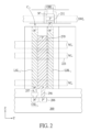
10 基板
111 垂直NORストリング
112 グローバルソース線 (GSL)、信号ライン
113 ワード線(WL)
114 グローバルビット線(GBL)、信号ライン
200 基板
206 柱身バイアスソース
211 ビットラインアクセス選択トランジスタ
223 ワード線
256 コンタクト
257 コンタクト
270 垂直NORストリングのTFT
310 絶縁分離
314-0~314-7 グローバルビット線(GBL)
320、320a、320b チャネルブレーカ
323p ワード線スタック
334 電荷蓄積素子
354a~354d ローカルビット線(LBL)
355、355a~355d ローカルソース線(LSL)
356 チャネル領域、環状シリコンチャネル
356a、356b、356-1~356-8 チャネル領域
Claims (16)
- 基板と、
前記基板上方に配置された、垂直方向に沿って延在する半導体材料の円柱と、
前記円柱の周りを覆っているワード線スタックと、
前記ワード線スタックと前記円柱との間に配置された電荷蓄積要素と、を含み、前記円柱、前記電荷蓄積要素、および前記ワード線スタックは、少なくとも2つのメモリセルを構成する、3次元フラッシュメモリデバイスであって、
前記少なくとも2つのメモリセルのうちの2つは、前記垂直方向に沿って延在する共通のローカルソース線を含み、
前記少なくとも2つのメモリセルのうちの2つは、前記垂直方向に沿って延在し、前記少なくとも2つのメモリセルのうちの2つを分離する、チャネルブレーカを含み、
前記円柱は、前記垂直方向に沿って延在する、少なくとも2つのローカルビット線および前記共通のローカルソース線を備え、
前記3次元フラッシュメモリデバイスは、
前記少なくとも2つのローカルビット線のうちの第1のローカルビット線と、前記共通のローカルソース線との間の第1のチャネル領域と、
前記少なくとも2つのローカルビット線のうちの第2のローカルビット線と、前記共通のローカルソース線との間の第2のチャネル領域と、を含み、
前記チャネルブレーカは、前記第1のチャネル領域を前記第2のチャネル領域から分離する、
3次元フラッシュメモリデバイス。 - 前記チャネルブレーカは、絶縁層を含む、請求項1に記載の3次元フラッシュメモリデバイス。
- 前記チャネルブレーカは、前記少なくとも2つのローカルビット線を分離することによって前記少なくとも2つのメモリセルを分離する、請求項1に記載の3次元フラッシュメモリデバイス。
- ワード線を含む前記ワード線スタックが、前記垂直方向と直角をなす第2の方向に沿って延在する、請求項3に記載の3次元フラッシュメモリデバイス。
- 前記少なくとも2つのメモリセルのうちの2つは、前記ワード線および前記少なくとも2つのローカルビット線によって制御されるように構成される、請求項4に記載の3次元フラッシュメモリデバイス。
- 前記少なくとも2つのローカルビット線が、2つのグローバルビット線にそれぞれ電気的に結合されている、請求項4に記載の3次元フラッシュメモリデバイス。
- 前記2つのグローバルビット線が、前記第2の方向および前記垂直方向と直角をなす第3の方向に沿って延在する、請求項6に記載の3次元フラッシュメモリデバイス。
- 前記2つのグローバルビット線が、選択トランジスタに電気的に結合されており、前記選択トランジスタが、前記2つのグローバルビット線を前記少なくとも2つのローカルビット線に接続する、請求項6に記載の3次元フラッシュメモリデバイス。
- 基板と、
前記基板上方に配置された半導体材料の複数の円柱であって、前記複数の円柱の各々が、垂直方向に沿って延在する、複数の円柱と、
前記複数の円柱の周りを覆っているワード線スタックと、
前記ワード線スタックと前記複数の円柱の各々との間に配置された電荷蓄積要素と、を含み、前記複数の円柱の各々、前記電荷蓄積要素、および前記ワード線スタックは、複数のメモリセルを構成し、
前記複数のメモリセルは、前記垂直方向に沿って延在する少なくとも1つの共通のローカルソース線を含み、
前記複数の円柱の各々は、前記垂直方向に沿って延在する、複数のローカルビット線および複数のローカルソース線を備え、複数のチャネル領域が、前記複数のローカルビット線と複数のローカルソース線との間に配置されており、
前記複数のチャネル領域のうちの2つの間を分離するチャネルブレーカをさらに備える、
3次元フラッシュメモリデバイス。 - 前記複数のメモリセルのうちの各々2つは、前記垂直方向に沿って延在する、少なくとも2つのローカルビット線および前記少なくとも1つの共通のローカルソース線を備える、請求項9に記載の3次元フラッシュメモリデバイス。
- ワード線を含む前記ワード線スタックが、前記垂直方向と直角をなす第2の方向に沿って延在する、請求項10に記載の3次元フラッシュメモリデバイス。
- 前記複数のメモリセルのうちの各々2つは、ワード線および前記少なくとも2つのローカルビット線によって制御されるように構成される、請求項11に記載の3次元フラッシュメモリデバイス。
- 前記複数のローカルビット線が、複数のグローバルビット線にそれぞれ電気的に結合されている、請求項11に記載の3次元フラッシュメモリデバイス。
- 前記複数のグローバルビット線が、前記第2の方向および前記垂直方向と直角をなす第3の方向に沿って延在する、請求項13に記載の3次元フラッシュメモリデバイス。
- 前記複数のグローバルビット線の各々が、選択トランジスタに電気的に結合されており、前記選択トランジスタが、前記複数のグローバルビット線を前記複数のローカルビット線に接続する、請求項13に記載の3次元フラッシュメモリデバイス。
- 前記チャネルブレーカが、前記複数のローカルビット線のうちの2つの間に配置される、請求項9に記載の3次元フラッシュメモリデバイス。
Applications Claiming Priority (1)
| Application Number | Priority Date | Filing Date | Title |
|---|---|---|---|
| PCT/CN2019/093678 WO2020258246A1 (en) | 2019-06-28 | 2019-06-28 | Three-dimensional flash memory device with increased storage density |
Publications (2)
| Publication Number | Publication Date |
|---|---|
| JP2022538095A JP2022538095A (ja) | 2022-08-31 |
| JP7325552B2 true JP7325552B2 (ja) | 2023-08-14 |
Family
ID=68634396
Family Applications (1)
| Application Number | Title | Priority Date | Filing Date |
|---|---|---|---|
| JP2021576379A Active JP7325552B2 (ja) | 2019-06-28 | 2019-06-28 | 高記憶密度化3次元フラッシュメモリデバイス |
Country Status (7)
| Country | Link |
|---|---|
| US (2) | US11211400B2 (ja) |
| EP (1) | EP3963628B1 (ja) |
| JP (1) | JP7325552B2 (ja) |
| KR (1) | KR102672972B1 (ja) |
| CN (2) | CN110520990B (ja) |
| TW (1) | TWI725648B (ja) |
| WO (1) | WO2020258246A1 (ja) |
Families Citing this family (21)
| Publication number | Priority date | Publication date | Assignee | Title |
|---|---|---|---|---|
| TWI848993B (zh) * | 2018-10-26 | 2024-07-21 | 美商蘭姆研究公司 | 三端子記憶體元件的自對準垂直集成 |
| US11729988B2 (en) * | 2020-06-18 | 2023-08-15 | Taiwan Semiconductor Manufacturing Company, Ltd. | Memory device comprising conductive pillars and method of forming the same |
| WO2022006776A1 (en) * | 2020-07-08 | 2022-01-13 | Yangtze Memory Technologies Co., Ltd. | Three-dimensional memory devices with channel structures having plum blossom shape |
| CN112106199B (zh) * | 2020-07-08 | 2024-04-16 | 长江存储科技有限责任公司 | 用于形成具有拥有梅花形状的沟道结构的三维存储器件的方法 |
| WO2022082346A1 (en) | 2020-10-19 | 2022-04-28 | Yangtze Memory Technologies Co., Ltd. | Three-dimensional memory devices with channel structures having plum blossom shape |
| WO2022082347A1 (en) | 2020-10-19 | 2022-04-28 | Yangtze Memory Technologies Co., Ltd. | Three-dimensional memory devices with channel structures having plum blossom shape and methods for forming the same |
| CN117881189A (zh) * | 2020-11-13 | 2024-04-12 | 武汉新芯集成电路制造有限公司 | 半导体器件 |
| TWI759015B (zh) * | 2020-12-17 | 2022-03-21 | 旺宏電子股份有限公司 | 三維記憶體元件及其製造方法 |
| US11778823B2 (en) | 2020-12-17 | 2023-10-03 | Macronix International Co., Ltd. | Three-dimensional memory device and method for manufacturing the same |
| US11758735B2 (en) * | 2021-02-25 | 2023-09-12 | Taiwan Semiconductor Manufacturing Company, Ltd. | Common-connection method in 3D memory |
| US11980035B2 (en) * | 2021-03-04 | 2024-05-07 | Taiwan Semiconductor Manufacturing Company, Ltd. | Three-dimensional memory devices and methods of manufacturing thereof |
| TWI763361B (zh) * | 2021-03-10 | 2022-05-01 | 旺宏電子股份有限公司 | 記憶體裝置及製造方法及其操作方法 |
| US12262540B2 (en) * | 2021-04-08 | 2025-03-25 | Taiwan Semiconductor Manufacturing Company, Ltd. | Semiconductor memory devices and methods of manufacturing thereof |
| US11647637B2 (en) * | 2021-08-20 | 2023-05-09 | Taiwan Semiconductor Manufacturing Company, Ltd. | Semiconductor memory devices and methods of manufacturing thereof |
| US11903203B2 (en) * | 2021-08-30 | 2024-02-13 | Macronix International Co., Ltd. | 3D and flash memory device and method of fabricating the same |
| US20230106571A1 (en) * | 2021-10-06 | 2023-04-06 | Macronix International Co., Ltd. | 3d nor and 3d nand memory integration |
| US12142656B2 (en) * | 2021-12-03 | 2024-11-12 | International Business Machines Corporation | Staggered stacked semiconductor devices |
| KR20240122985A (ko) * | 2023-02-06 | 2024-08-13 | 에스케이하이닉스 주식회사 | 반도체 장치 및 반도체 장치의 제조 방법 |
| US20250006261A1 (en) * | 2023-06-27 | 2025-01-02 | Micron Technology, Inc. | Memory device with segmented sgd drain |
| TWI857842B (zh) * | 2023-11-08 | 2024-10-01 | 旺宏電子股份有限公司 | 三維記憶體 |
| US12406735B2 (en) * | 2023-11-08 | 2025-09-02 | Macronix International Co., Ltd. | 3D memory |
Citations (4)
| Publication number | Priority date | Publication date | Assignee | Title |
|---|---|---|---|---|
| US20160099254A1 (en) | 2014-10-03 | 2016-04-07 | Sandisk Technologies Inc. | Memory Hole Structure in Three Dimensional Memory |
| US20170148517A1 (en) | 2015-11-25 | 2017-05-25 | Eli Harari | Three-dimensional vertical nor flash thin film transistor strings |
| WO2017091338A1 (en) | 2015-11-25 | 2017-06-01 | Eli Harari | Three-dimensional vertical nor flash thin film transistor strings |
| US20180182776A1 (en) | 2016-12-22 | 2018-06-28 | Samsung Electronics Co., Ltd. | Vertical memory devices |
Family Cites Families (24)
| Publication number | Priority date | Publication date | Assignee | Title |
|---|---|---|---|---|
| TW406419B (en) * | 1998-01-15 | 2000-09-21 | Siemens Ag | Memory-cells arrangement and its production method |
| US6536719B2 (en) | 2001-07-17 | 2003-03-25 | .Engineering, Inc. | Single-handed cord/cable management device |
| TW569378B (en) | 2002-07-25 | 2004-01-01 | Taiwan Semiconductor Mfg | Structure with L-shape word line spacer and fabricating method thereof |
| KR100909627B1 (ko) | 2007-10-10 | 2009-07-27 | 주식회사 하이닉스반도체 | 플래시 메모리소자 |
| KR101469106B1 (ko) * | 2008-07-02 | 2014-12-05 | 삼성전자주식회사 | 3차원 반도체 장치, 그 동작 방법 및 제조 방법 |
| WO2012002186A1 (en) | 2010-07-02 | 2012-01-05 | Semiconductor Energy Laboratory Co., Ltd. | Semiconductor device |
| KR101780274B1 (ko) * | 2011-05-04 | 2017-09-21 | 에스케이하이닉스 주식회사 | 비휘발성 메모리 장치 |
| US9147493B2 (en) * | 2013-06-17 | 2015-09-29 | Micron Technology, Inc. | Shielded vertically stacked data line architecture for memory |
| KR102128465B1 (ko) * | 2014-01-03 | 2020-07-09 | 삼성전자주식회사 | 수직 구조의 비휘발성 메모리 소자 |
| KR102145062B1 (ko) * | 2014-03-17 | 2020-08-18 | 에스케이하이닉스 주식회사 | 반도체 장치 |
| US9666594B2 (en) * | 2014-09-05 | 2017-05-30 | Sandisk Technologies Llc | Multi-charge region memory cells for a vertical NAND device |
| US9418750B2 (en) * | 2014-09-15 | 2016-08-16 | Sandisk Technologies Llc | Single ended word line and bit line time constant measurement |
| US20170062456A1 (en) * | 2015-08-31 | 2017-03-02 | Cypress Semiconductor Corporation | Vertical division of three-dimensional memory device |
| US9858009B2 (en) | 2015-10-26 | 2018-01-02 | Sandisk Technologies Llc | Data folding in 3D nonvolatile memory |
| TWI572018B (zh) | 2015-10-28 | 2017-02-21 | 旺宏電子股份有限公司 | 記憶體元件及其製作方法 |
| US10103155B2 (en) * | 2016-03-09 | 2018-10-16 | Toshiba Memory Corporation | Semiconductor memory device |
| US9847342B2 (en) * | 2016-03-14 | 2017-12-19 | Toshiba Memory Corporation | Semiconductor memory device and method for manufacturing same |
| KR102637644B1 (ko) * | 2016-07-14 | 2024-02-19 | 삼성전자주식회사 | 메모리 장치 |
| WO2018144957A1 (en) * | 2017-02-04 | 2018-08-09 | Monolithic 3D Inc. | 3d semiconductor device and structure |
| CN107527919A (zh) * | 2017-08-31 | 2017-12-29 | 长江存储科技有限责任公司 | 一种3d nand存储器件及其制造方法 |
| CN109698162A (zh) * | 2017-10-20 | 2019-04-30 | 萨摩亚商费洛储存科技股份有限公司 | 三维存储元件及其制造方法 |
| CN107863348B (zh) * | 2017-11-01 | 2019-03-12 | 长江存储科技有限责任公司 | 一种3d nand存储器件及其制造方法 |
| CN107994033B (zh) * | 2017-11-16 | 2020-05-12 | 长江存储科技有限责任公司 | 一种基于氧化物-多晶硅薄膜堆叠的3d nand沟道孔成形方法 |
| CN109801922B (zh) * | 2019-01-31 | 2020-10-20 | 长江存储科技有限责任公司 | 一种形成三维存储器的方法及三维存储器 |
-
2019
- 2019-06-28 EP EP19935539.7A patent/EP3963628B1/en active Active
- 2019-06-28 CN CN201980001326.7A patent/CN110520990B/zh active Active
- 2019-06-28 CN CN202010498902.8A patent/CN111613623B/zh active Active
- 2019-06-28 WO PCT/CN2019/093678 patent/WO2020258246A1/en not_active Ceased
- 2019-06-28 KR KR1020217041725A patent/KR102672972B1/ko active Active
- 2019-06-28 JP JP2021576379A patent/JP7325552B2/ja active Active
- 2019-11-29 US US16/699,121 patent/US11211400B2/en active Active
- 2019-12-03 TW TW108144109A patent/TWI725648B/zh active
-
2021
- 2021-10-13 US US17/500,370 patent/US11956962B2/en active Active
Patent Citations (5)
| Publication number | Priority date | Publication date | Assignee | Title |
|---|---|---|---|---|
| US20160099254A1 (en) | 2014-10-03 | 2016-04-07 | Sandisk Technologies Inc. | Memory Hole Structure in Three Dimensional Memory |
| US20170148517A1 (en) | 2015-11-25 | 2017-05-25 | Eli Harari | Three-dimensional vertical nor flash thin film transistor strings |
| WO2017091338A1 (en) | 2015-11-25 | 2017-06-01 | Eli Harari | Three-dimensional vertical nor flash thin film transistor strings |
| JP2019504479A (ja) | 2015-11-25 | 2019-02-14 | サンライズ メモリー コーポレイション | 3次元垂直norフラッシュ薄膜トランジスタストリング |
| US20180182776A1 (en) | 2016-12-22 | 2018-06-28 | Samsung Electronics Co., Ltd. | Vertical memory devices |
Also Published As
| Publication number | Publication date |
|---|---|
| EP3963628A4 (en) | 2022-12-14 |
| CN111613623B (zh) | 2021-02-19 |
| WO2020258246A1 (en) | 2020-12-30 |
| CN110520990B (zh) | 2020-05-22 |
| EP3963628A1 (en) | 2022-03-09 |
| US11211400B2 (en) | 2021-12-28 |
| US11956962B2 (en) | 2024-04-09 |
| TW202101679A (zh) | 2021-01-01 |
| JP2022538095A (ja) | 2022-08-31 |
| TWI725648B (zh) | 2021-04-21 |
| KR102672972B1 (ko) | 2024-06-05 |
| EP3963628B1 (en) | 2023-12-06 |
| US20200411539A1 (en) | 2020-12-31 |
| CN110520990A (zh) | 2019-11-29 |
| US20220045099A1 (en) | 2022-02-10 |
| KR20220010027A (ko) | 2022-01-25 |
| CN111613623A (zh) | 2020-09-01 |
Similar Documents
| Publication | Publication Date | Title |
|---|---|---|
| JP7325552B2 (ja) | 高記憶密度化3次元フラッシュメモリデバイス | |
| US10262739B2 (en) | Devices including memory arrays, row decoder circuitries and column decoder circuitries | |
| CN112420715A (zh) | 包含阵列下缓冲器电路系统的多层存储器装置 | |
| US11011208B2 (en) | Semiconductor memory device including parallel substrates in three dimensional structures | |
| US11605588B2 (en) | Memory device including data lines on multiple device levels | |
| KR20100032211A (ko) | 비휘발성 메모리 소자 및 그 동작 방법 | |
| US20240420766A1 (en) | Memory device including in-tier driver circuit | |
| US11798631B2 (en) | Transfer latch tiers | |
| CN115623787A (zh) | 集成组合件及形成集成组合件的方法 | |
| US20250380420A1 (en) | Memory device including concentric conductive contacts | |
| US20250372168A1 (en) | Memory device including conductive contacts in treated tiers | |
| US12010847B2 (en) | Foundational supports within integrated assemblies | |
| US20260075829A1 (en) | Memory device including control gates having partial dielectric liners | |
| US20250378857A1 (en) | Memory device including conductive contacts and support structures | |
| US20250372169A1 (en) | Memory device including conductive contacts aligned with support structures | |
| US20260033318A1 (en) | Memory device including conductive contacts with multiple liners | |
| TW202608224A (zh) | 包含經處理層中之導電觸件之記憶體裝置 | |
| TW202608223A (zh) | 包含與支撐結構對齊之導電接觸件之記憶體裝置 | |
| TW202614775A (zh) | 包含具有多個襯墊之導電觸點之記憶體裝置 |
Legal Events
| Date | Code | Title | Description |
|---|---|---|---|
| A521 | Request for written amendment filed |
Free format text: JAPANESE INTERMEDIATE CODE: A523 Effective date: 20211221 |
|
| A621 | Written request for application examination |
Free format text: JAPANESE INTERMEDIATE CODE: A621 Effective date: 20211221 |
|
| A131 | Notification of reasons for refusal |
Free format text: JAPANESE INTERMEDIATE CODE: A131 Effective date: 20230110 |
|
| A521 | Request for written amendment filed |
Free format text: JAPANESE INTERMEDIATE CODE: A523 Effective date: 20230328 |
|
| TRDD | Decision of grant or rejection written | ||
| A01 | Written decision to grant a patent or to grant a registration (utility model) |
Free format text: JAPANESE INTERMEDIATE CODE: A01 Effective date: 20230703 |
|
| A61 | First payment of annual fees (during grant procedure) |
Free format text: JAPANESE INTERMEDIATE CODE: A61 Effective date: 20230801 |
|
| R150 | Certificate of patent or registration of utility model |
Ref document number: 7325552 Country of ref document: JP Free format text: JAPANESE INTERMEDIATE CODE: R150 |