JP7325552B2 - High storage density 3D flash memory device - Google Patents
High storage density 3D flash memory device Download PDFInfo
- Publication number
- JP7325552B2 JP7325552B2 JP2021576379A JP2021576379A JP7325552B2 JP 7325552 B2 JP7325552 B2 JP 7325552B2 JP 2021576379 A JP2021576379 A JP 2021576379A JP 2021576379 A JP2021576379 A JP 2021576379A JP 7325552 B2 JP7325552 B2 JP 7325552B2
- Authority
- JP
- Japan
- Prior art keywords
- local
- flash memory
- memory device
- bit lines
- channel
- Prior art date
- Legal status (The legal status is an assumption and is not a legal conclusion. Google has not performed a legal analysis and makes no representation as to the accuracy of the status listed.)
- Active
Links
Images


Classifications
-
- H—ELECTRICITY
- H10—SEMICONDUCTOR DEVICES; ELECTRIC SOLID-STATE DEVICES NOT OTHERWISE PROVIDED FOR
- H10B—ELECTRONIC MEMORY DEVICES
- H10B43/00—EEPROM devices comprising charge-trapping gate insulators
- H10B43/20—EEPROM devices comprising charge-trapping gate insulators characterised by three-dimensional [3D] arrangements, e.g. with cells on different height levels
- H10B43/23—EEPROM devices comprising charge-trapping gate insulators characterised by three-dimensional [3D] arrangements, e.g. with cells on different height levels with source and drain on different levels, e.g. with sloping channels
- H10B43/27—EEPROM devices comprising charge-trapping gate insulators characterised by three-dimensional [3D] arrangements, e.g. with cells on different height levels with source and drain on different levels, e.g. with sloping channels the channels comprising vertical portions, e.g. U-shaped channels
-
- H—ELECTRICITY
- H10—SEMICONDUCTOR DEVICES; ELECTRIC SOLID-STATE DEVICES NOT OTHERWISE PROVIDED FOR
- H10B—ELECTRONIC MEMORY DEVICES
- H10B41/00—Electrically erasable-and-programmable ROM [EEPROM] devices comprising floating gates
- H10B41/20—Electrically erasable-and-programmable ROM [EEPROM] devices comprising floating gates characterised by three-dimensional [3D] arrangements, e.g. with cells on different height levels
-
- H—ELECTRICITY
- H10—SEMICONDUCTOR DEVICES; ELECTRIC SOLID-STATE DEVICES NOT OTHERWISE PROVIDED FOR
- H10B—ELECTRONIC MEMORY DEVICES
- H10B43/00—EEPROM devices comprising charge-trapping gate insulators
- H10B43/30—EEPROM devices comprising charge-trapping gate insulators characterised by the memory core region
- H10B43/35—EEPROM devices comprising charge-trapping gate insulators characterised by the memory core region with cell select transistors, e.g. NAND
-
- H—ELECTRICITY
- H10—SEMICONDUCTOR DEVICES; ELECTRIC SOLID-STATE DEVICES NOT OTHERWISE PROVIDED FOR
- H10B—ELECTRONIC MEMORY DEVICES
- H10B41/00—Electrically erasable-and-programmable ROM [EEPROM] devices comprising floating gates
- H10B41/30—Electrically erasable-and-programmable ROM [EEPROM] devices comprising floating gates characterised by the memory core region
- H10B41/35—Electrically erasable-and-programmable ROM [EEPROM] devices comprising floating gates characterised by the memory core region with a cell select transistor, e.g. NAND
-
- H—ELECTRICITY
- H10—SEMICONDUCTOR DEVICES; ELECTRIC SOLID-STATE DEVICES NOT OTHERWISE PROVIDED FOR
- H10B—ELECTRONIC MEMORY DEVICES
- H10B43/00—EEPROM devices comprising charge-trapping gate insulators
- H10B43/10—EEPROM devices comprising charge-trapping gate insulators characterised by the top-view layout
-
- H—ELECTRICITY
- H10—SEMICONDUCTOR DEVICES; ELECTRIC SOLID-STATE DEVICES NOT OTHERWISE PROVIDED FOR
- H10B—ELECTRONIC MEMORY DEVICES
- H10B43/00—EEPROM devices comprising charge-trapping gate insulators
- H10B43/20—EEPROM devices comprising charge-trapping gate insulators characterised by three-dimensional [3D] arrangements, e.g. with cells on different height levels
-
- H—ELECTRICITY
- H10—SEMICONDUCTOR DEVICES; ELECTRIC SOLID-STATE DEVICES NOT OTHERWISE PROVIDED FOR
- H10B—ELECTRONIC MEMORY DEVICES
- H10B43/00—EEPROM devices comprising charge-trapping gate insulators
- H10B43/40—EEPROM devices comprising charge-trapping gate insulators characterised by the peripheral circuit region
-
- H—ELECTRICITY
- H10—SEMICONDUCTOR DEVICES; ELECTRIC SOLID-STATE DEVICES NOT OTHERWISE PROVIDED FOR
- H10B—ELECTRONIC MEMORY DEVICES
- H10B43/00—EEPROM devices comprising charge-trapping gate insulators
- H10B43/50—EEPROM devices comprising charge-trapping gate insulators characterised by the boundary region between the core and peripheral circuit regions
-
- H—ELECTRICITY
- H10—SEMICONDUCTOR DEVICES; ELECTRIC SOLID-STATE DEVICES NOT OTHERWISE PROVIDED FOR
- H10D—INORGANIC ELECTRIC SEMICONDUCTOR DEVICES
- H10D64/00—Electrodes of devices having potential barriers
- H10D64/60—Electrodes characterised by their materials
- H10D64/66—Electrodes having a conductor capacitively coupled to a semiconductor by an insulator, e.g. MIS electrodes
- H10D64/68—Electrodes having a conductor capacitively coupled to a semiconductor by an insulator, e.g. MIS electrodes characterised by the insulator, e.g. by the gate insulator
- H10D64/693—Electrodes having a conductor capacitively coupled to a semiconductor by an insulator, e.g. MIS electrodes characterised by the insulator, e.g. by the gate insulator the insulator comprising nitrogen, e.g. nitrides, oxynitrides or nitrogen-doped materials
-
- H—ELECTRICITY
- H10—SEMICONDUCTOR DEVICES; ELECTRIC SOLID-STATE DEVICES NOT OTHERWISE PROVIDED FOR
- H10W—GENERIC PACKAGES, INTERCONNECTIONS, CONNECTORS OR OTHER CONSTRUCTIONAL DETAILS OF DEVICES COVERED BY CLASS H10
- H10W20/00—Interconnections in chips, wafers or substrates
- H10W20/40—Interconnections external to wafers or substrates, e.g. back-end-of-line [BEOL] metallisations or vias connecting to gate electrodes
- H10W20/41—Interconnections external to wafers or substrates, e.g. back-end-of-line [BEOL] metallisations or vias connecting to gate electrodes characterised by their conductive parts
- H10W20/43—Layouts of interconnections
Landscapes
- Semiconductor Memories (AREA)
- Non-Volatile Memory (AREA)
- Physics & Mathematics (AREA)
- Geometry (AREA)
Description
本開示は、メモリデバイスに関し、より詳細には、高記憶密度化3次元(3D)NORフラッシュメモリデバイスに関する。 TECHNICAL FIELD The present disclosure relates to memory devices and, more particularly, to densified three-dimensional (3D) NOR flash memory devices.
フラッシュメモリデバイスは、記憶されたデータが電気的に消去または書き込み可能な(すなわち、プログラミング可能な)不揮発性メモリデバイスである。実際に、フラッシュメモリデバイスは、単一の処理で消去でき、電気的にプログラミング可能であるので、コンピュータおよびメモリカードに広く使用されている。 Flash memory devices are non-volatile memory devices in which the data stored can be electrically erased or written (ie, programmable). In fact, flash memory devices are widely used in computers and memory cards because they can be erased in a single operation and are electrically programmable.
読出し動作用のロジックゲートに基づくフラッシュメモリには2つの主要な種類、NANDタイプおよびNORタイプがある。NORフラッシュメモリに関して、あらゆる個々のメモリセルが別々に読み出されまたは変更され得、それにより完全なランダムアクセスを提供し、そのため、揮発性SRAMまたはDRAMを置換する、不揮発性を有する実行可能なコード記憶装置として使用され得る。 There are two main types of flash memory based on logic gates for read operations, NAND type and NOR type. For NOR flash memory, non-volatile executable code in which every individual memory cell can be read or modified separately, thereby providing completely random access, thus replacing volatile SRAM or DRAM It can be used as a storage device.
当技術分野で知られているように、NORメモリストリングまたはNORストリングは、多くの記憶トランジスタを含み、その各々が共有ソース領域および共有ドレイン領域に接続されている。そのため、NORストリングのトランジスタは、並列に接続されている。NORストリング内の記憶トランジスタを読み出すまたはプログラミングするために、その記憶トランジスタのみが、アクティブ化される(すなわち、「オン」または導通)必要があり、NORストリング内の他のすべての記憶トランジスタは、休止状態(すなわち、「オフ」または非導通)のままである。したがって、NORストリングは、読み出されるアクティブ化された記憶トランジスタの非常に速い検知を可能にする。 As is known in the art, a NOR memory string or NOR string includes many storage transistors, each connected to shared source and drain regions. Therefore, the transistors of the NOR string are connected in parallel. To read or program a storage transistor within a NOR string, only that storage transistor needs to be activated (i.e., "on" or conducting); all other storage transistors within the NOR string are quiescent. remain in the state (ie, "off" or non-conducting). Therefore, the NOR string allows very fast sensing of the activated storage transistor being read.
従来のNORトランジスタは、電子がソース領域とドレイン領域との間の電圧差によってチャネル領域で加速され、適切な電圧が制御ゲートに印加されているときに制御ゲートとチャネル領域との間の電荷捕捉層内に注入される、チャネルホットエレクトロン(CHE)注入法によってプログラミングされる。 In a conventional NOR transistor, electrons are accelerated in the channel region by a voltage difference between the source and drain regions, causing charge trapping between the control gate and the channel region when an appropriate voltage is applied to the control gate. It is programmed by channel hot electron (CHE) injection, which is injected into the layer.
フラッシュメモリチップの連続する世代とともに、製造コストを最小化する一方で、アレイ密度を増大させチップ面積を最大化することに、重点が置かれ続けている。目下の工程フローの最小限の変更でまたは変更せずに、フラッシュメモリデバイスの記憶密度を増大させることが、さらに所望されている。 With successive generations of flash memory chips, the emphasis continues to be on increasing array density and maximizing chip area while minimizing manufacturing costs. It is further desired to increase the storage density of flash memory devices with minimal or no change in current process flows.
改善された高記憶密度化3次元(3D)NORフラッシュメモリデバイスを提供することが、本開示の一目的である。 It is an object of the present disclosure to provide an improved densified three-dimensional (3D) NOR flash memory device.
本開示の一態様によれば、3次元フラッシュメモリデバイスは、十分な平坦面を有する基板を含む。半導体材料の複数の活性円柱が、基板上に配置されている。複数の活性円柱の各々は、基板の平坦面に直交する第1の方向に沿って延在する。複数の活性円柱は、2次元のアレイに配設されている。複数の活性円柱の各々は、第1の方向に沿って延在する、少なくとも2つのローカルビット線および少なくとも1つのローカルソース線を備える。第1のチャネル領域が、少なくとも2つのローカルビット線のうちの第1のローカルビット線と、少なくとも1つのローカルソース線との間に配置されている。第2のチャネル領域が、少なくとも2つのローカルビット線のうちの第2のローカルビット線と、少なくとも1つのローカルソース線との間に配置されている。ワード線スタックが、複数の活性円柱の周りを覆っている。電荷蓄積要素が、ワード線スタックと複数の活性円柱の各々との間に配置されている。 According to one aspect of the disclosure, a three-dimensional flash memory device includes a substrate having a substantially flat surface. A plurality of active columns of semiconductor material are disposed on the substrate. Each of the plurality of active columns extends along a first direction orthogonal to the planar surface of the substrate. A plurality of active cylinders are arranged in a two-dimensional array. Each of the plurality of active columns comprises at least two local bit lines and at least one local source line extending along the first direction. A first channel region is disposed between a first local bit line of the at least two local bit lines and at least one local source line. A second channel region is disposed between a second local bit line of the at least two local bit lines and the at least one local source line. A word line stack wraps around a plurality of active columns. A charge storage element is positioned between the word line stack and each of the plurality of active columns.
いくつかの実施形態によれば、ワード線スタックは、基板の平坦面に平行な第2の方向に沿って延在する。 According to some embodiments, the word line stacks extend along a second direction parallel to the planar surface of the substrate.
いくつかの実施形態によれば、少なくとも2つのローカルビット線が、2つのグローバルビット線にそれぞれ電気的に結合されている。 According to some embodiments, at least two local bitlines are electrically coupled to two global bitlines, respectively.
いくつかの実施形態によれば、2つのグローバルビット線は、第2の方向に平行でなく、基板の平坦面に平行な第3の方向に沿って延在する。 According to some embodiments, the two global bit lines extend along a third direction parallel to the planar surface of the substrate, non-parallel to the second direction.
いくつかの実施形態によれば、2つのグローバルビット線の各々は、ビットラインアクセス選択トランジスタに電気的に結合されており、ビットラインアクセス選択トランジスタは、2つのグローバルビット線の各々を少なくとも2つのローカルビット線の各々に接続する。 According to some embodiments, each of the two global bitlines is electrically coupled to a bitline access select transistor, the bitline access select transistor connecting each of the two global bitlines to at least two global bitlines. Connect to each of the local bit lines.
いくつかの実施形態によれば、電荷蓄積要素は、電荷捕捉層を含む。 According to some embodiments, the charge storage element includes a charge trapping layer.
いくつかの実施形態によれば、電荷捕捉層は、窒化シリコンを含む。 According to some embodiments, the charge trapping layer comprises silicon nitride.
いくつかの実施形態によれば、3次元フラッシュメモリデバイスは、第1のチャネル領域を第2のチャネル領域から分離する、チャネルブレーカをさらに備える。 According to some embodiments, the 3D flash memory device further comprises a channel breaker separating the first channel region from the second channel region.
いくつかの実施形態によれば、複数の活性円柱は、互い違いに配設されている。 According to some embodiments, the plurality of active columns are staggered.
いくつかの実施形態によれば、基板は、シリコン基板を含む。 According to some embodiments, the substrate comprises a silicon substrate.
本開示の別の態様によれば、3次元フラッシュメモリデバイスは、十分な平坦面を有する基板を含む。半導体材料の複数の活性円柱が、基板上に配置される。複数の活性円柱の各々は、基板の平坦面に直交する第1の方向に沿って延在する。複数の活性円柱は、2次元のアレイに配設されている。複数の活性円柱の各々は、第1の方向に沿って延在する、複数のローカルビット線および複数のローカルソース線を備える。複数のチャネル領域が、複数のローカルビット線と複数のローカルソース線との間に配置されている。ワード線スタックが、複数の活性円柱の周りを覆っている。電荷蓄積要素が、ワード線スタックと複数の活性円柱の各々との間に配置されている。 According to another aspect of the disclosure, a three-dimensional flash memory device includes a substrate having a substantially planar surface. A plurality of active columns of semiconductor material are disposed on the substrate. Each of the plurality of active columns extends along a first direction orthogonal to the planar surface of the substrate. A plurality of active cylinders are arranged in a two-dimensional array. Each of the plurality of active columns comprises a plurality of local bit lines and a plurality of local source lines extending along the first direction. A plurality of channel regions are disposed between the plurality of local bit lines and the plurality of local source lines. A word line stack wraps around a plurality of active columns. A charge storage element is positioned between the word line stack and each of the plurality of active columns.
いくつかの実施形態によれば、ワード線スタックは、基板の平坦面に平行な第2の方向に沿って延在する。 According to some embodiments, the word line stacks extend along a second direction parallel to the planar surface of the substrate.
いくつかの実施形態によれば、複数のローカルビット線は、複数のグローバルビット線にそれぞれ電気的に結合されている。 According to some embodiments, the plurality of local bitlines are each electrically coupled to the plurality of global bitlines.
いくつかの実施形態によれば、複数のグローバルビット線は、第2の方向に平行でなく、基板の平坦面に平行な第3の方向に沿って延在する。 According to some embodiments, the plurality of global bit lines extends along a third direction parallel to the planar surface of the substrate, non-parallel to the second direction.
いくつかの実施形態によれば、複数のグローバルビット線の各々は、ビットラインアクセス選択トランジスタに電気的に結合されており、ビットラインアクセス選択トランジスタは、複数のグローバルビット線の各々を複数のローカルビット線の各々に接続する。 According to some embodiments, each of the plurality of global bitlines is electrically coupled to a bitline access select transistor, the bitline access select transistor connecting each of the plurality of global bitlines to the plurality of local bitlines. Connect to each of the bit lines.
いくつかの実施形態によれば、電荷蓄積要素は、電荷捕捉層を含む。 According to some embodiments, the charge storage element includes a charge trapping layer.
いくつかの実施形態によれば、電荷捕捉層は、窒化シリコンを含む。 According to some embodiments, the charge trapping layer comprises silicon nitride.
いくつかの実施形態によれば、3次元フラッシュメモリデバイスは、複数のローカルビット線のうちの2つの間のチャネルブレーカをさらに備える。 According to some embodiments, the 3D flash memory device further comprises a channel breaker between two of the plurality of local bitlines.
いくつかの実施形態によれば、複数の活性円柱は、互い違いに配設されている。 According to some embodiments, the plurality of active columns are staggered.
いくつかの実施形態によれば、基板は、シリコン基板を含む。 According to some embodiments, the substrate comprises a silicon substrate.
本発明のこれらの目的および他の目的は、以下の、多様な図形および図画で図示されている好ましい実施形態の詳細な説明を読むことで、当業者にはおそらく明白になるであろう。 These and other objects of the present invention will likely become apparent to those skilled in the art upon reading the following detailed description of preferred embodiments illustrated in various figures and drawings.
本明細書に組み込まれ、明細書の一部を形成する添付図面は、本開示の実施形態を図解し、記述と共に、本開示の原理を説明し、当業者が本開示を製造し、使用することを可能にすることに、さらに助力する。 The accompanying drawings, which are incorporated in and form a part of the specification, illustrate embodiments of the disclosure and, together with the description, serve to explain the principles of the disclosure and to enable one skilled in the art to make and use the disclosure. further help to make it possible.
本開示の実施形態が、添付図面を参照して説明されることになる。 Embodiments of the present disclosure will be described with reference to the accompanying drawings.
ここで、本開示を理解し、実施し、技術的効果を実感するために、添付図面において図示されている、本発明の例示的な実施形態への参照が、詳細になされることになる。以下の説明が、一例としてのみなされ、しかしながら本開示を限定するためになされていないことが、理解されよう。本開示の多様な実施形態および実施形態内の互いに矛盾しない多様な特徴は、多様な方法で組み合わせられ、再編成され得る。本開示の主旨および範囲から逸脱することなく、本開示への変形例、同等物、または改善は、当業者に理解可能であり、本開示の範囲内に包括的に含まれることが意図されている。 In order to understand, practice, and appreciate the technical advantages of this disclosure, reference will now be made in detail to exemplary embodiments of the invention, as illustrated in the accompanying drawings. It will be appreciated that the following description is taken as an example only, but not to limit the present disclosure. Various embodiments of the present disclosure and various features consistent with each other within the embodiments can be combined and rearranged in various ways. Modifications, equivalents, or improvements to this disclosure, without departing from the spirit and scope of this disclosure, may be apparent to those skilled in the art and are intended to be encompassed within the scope of this disclosure. there is
明細書内での「ある実施形態」、「実施形態」、「例示的な実施形態」、「いくつかの実施形態」などへの参照は、記述された実施形態が特定の機能、構造、または特徴を含み得るが、あらゆる実施形態が必ずしも特定の形体、構造、または特徴を含まなくてもよい、ことを示すことに留意されたい。また、そのような語句は、必ずしも同一の実施形態を参照しない。 References in the specification to "an embodiment," "an embodiment," "exemplary embodiment," "some embodiments," etc., indicate that the described embodiments have a particular function, structure, or Note that although features may be included, not all embodiments may necessarily include a particular form, structure, or feature. Moreover, such phrases are not necessarily referring to the same embodiment.
さらに、特定の形体、構造、または特徴が、ある実施形態と連絡して記述されている場合、それが他の実施形態と連絡するそのような特定の形体、構造、または特徴に影響を及ぼすことは、明示的に記述されているか否かにかかわらず、当業者には自明のことであろう。 Further, if a particular feature, structure or characteristic is described in communication with one embodiment, it may affect such specific feature, structure or characteristic in communication with other embodiments. will be apparent to those skilled in the art, whether explicitly stated or not.
一般に、専門用語は、文脈内での使用法から少なくとも部分的に理解され得る。たとえば、本明細書で使用されているような「1つまたは複数の」という用語は、文脈に少なくとも部分的に依存して、任意の形体、構造、または特徴を単一の意味で記述するために使用され得る、あるいは形体、構造、または特徴の組み合わせを複数の意味で使用され得る。同様に、「a」、「an」、または「the」などの用語は、やはり文脈に少なくとも部分的に依存して、単一の語法を伝える、あるいは複数の語法を伝えると理解され得る。 In general, terminology can be understood, at least in part, from how it is used in context. For example, the term "one or more," as used herein, may be used to describe any feature, structure, or feature with a single meaning, depending at least in part on the context. or combinations of features, structures, or features may be used in multiple senses. Similarly, terms such as "a," "an," or "the" may be understood to convey a single usage or multiple usages, again depending at least in part on the context.
本開示内の「の上に(on)」、「より上に(above)」、「の上方に(over)」の意味は、最も広範に解釈されるべきであり、「の上に(on)」は、何か「の直接上に(on)」の意味だけでなく、それらの間に中間の形体または層を有して何か「の上に(on)」の意味も含み、「より上に(above)」、「の上方に(over)」は、何か「より上に(above)」、「の上方に(over)」を意味するだけでなく、それらの間に中間の形体または層を有さないで何か「より上に(above)」、「の上方に(over)」の意味(すなわち、何かの直接上)も含み得ることが容易に理解されるであろう。 The meanings of "on," "above," and "over" within this disclosure should be interpreted in the broadest possible terms, meaning "on )” includes not only the meaning “directly on” of something, but also the meaning “on” something with intermediate features or layers between them, "above", "over" means not only something "above", "over", but also something intermediate It will be readily understood that the meaning "above" or "over" something without having a feature or layer (i.e. directly on something) can also be included. deaf.
また、「の下に(beneath)」、「より下に(below)」、「下のほうの(lower)」、「より上に(above)」、「上のほうの(upper)」などの空間的に相対的な用語が、ある構成要素、もしくは形体の別の構成要素との関係、または図中で説明されているような形体の記述を記述しやすくするために、本明細書では使用されている場合がある。空間的に相対的な用語は、図中で表現されている向きに加えて、使用または動作中のデバイスの異なる向きを、包括的に含むことが意図されている。装置は、別の方向に向けられ(90度回転されまたは他の向きで)、本明細書で使用されている空間的に相対的な記述語が、それに応じて同様に解釈され得る。「垂直の」という用語は、半導体基板の表面に垂直な方向を指し、「水平の」という用語は、その半導体基板の表面に平行な任意の方向を指す。 Also, "beneath", "below", "lower", "above", "upper", etc. Spatially-relative terms are used herein to help describe the relationship of one component or feature to another, or the description of features such as those illustrated in the figures. may have been. Spatially-relative terms are intended to encompass different orientations of the device in use or operation in addition to the orientation depicted in the figures. The device may be otherwise oriented (rotated 90 degrees or at other orientations) and the spatially relative descriptors used herein similarly interpreted accordingly. The term "vertical" refers to a direction perpendicular to the surface of a semiconductor substrate, and the term "horizontal" refers to any direction parallel to the surface of the semiconductor substrate.
図1は、概念化されたメモリ構造1を示し、垂直NORストリング内に設けられたメモリセル(または記憶素子)の3次元構成を図解している。概念化されたメモリ構造1では、各垂直NORストリングは、本発明のある実施形態による、対応する水平ワード線によって各々が制御されるメモリセルを含む。概念化されたメモリ構造1では、各メモリセルは、「垂直に」配設されている、すなわち、基板10の表面に垂直な方向に沿って、堆積された薄膜内に形成されている。基板10は、たとえば、それらに限定されないが、集積回路製造に使用される、従来のシリコンウェハまたはシリコン基板であり得る。図1に示されているように、デカルト座標系が、単に説明を容易にするために採用されている。この座標系では、基板10表面は、X-Y平面に平行な平面としてみなされる。そのため、本明細書で使用されるように、「水平の」という用語は、X-Y平面に平行な任意の方向を指し、一方、「垂直の」は、Z方向を指す。
FIG. 1 shows a conceptualized
図1では、Z方向にある各々の垂直柱が、垂直NORストリング(たとえば、垂直NORストリング111)内の記憶素子またはTFTに相当する。垂直NORストリングは、X方向に沿って各々延在する列では、規則的に配設されている。同様の配置が、代わりに、Y方向に沿って各々延在する列の配置として見られ得る。垂直NORストリングの記憶素子は、垂直ローカルビット線を備え得、垂直ローカルソース線を共有し得る(図示せず)。水平ワード線(例えば、WL113)のスタックがY方向に沿って通っており、各ワード線は、Y方向に沿ったワード線に隣接して配置された垂直NORストリングの対応するTFT用の制御ゲートとして機能する。グローバルソース線(例えば、GSL112)およびグローバルビット線(GBL114)は、通常、概念化されたメモリ構造1の底部下方または上部上方のどちらかを通るX方向に沿って配設され得る。代わりに、信号ラインGSL112およびGBL114は、両方、概念化されたメモリ構造1の下方に、または上方に経路が定められ得、それらの各々は、アクセストランジスタ(図1に図示せず)によって個々の垂直NORストリングのローカルソース線およびローカルビット線に選択的に接続され得る。
In FIG. 1, each vertical column in the Z direction corresponds to a storage element or TFT within a vertical NOR string (eg, vertical NOR string 111). The vertical NOR strings are regularly arranged in columns each extending along the X direction. A similar arrangement can alternatively be seen as an arrangement of columns each extending along the Y direction. The storage elements of a vertical NOR string may comprise vertical local bit lines and may share vertical local source lines (not shown). A stack of horizontal word lines (e.g., WL113) runs along the Y direction, each word line being a control gate for a corresponding TFT in a vertical NOR string positioned adjacent to the word line along the Y direction. function as Global source lines (eg, GSL 112) and global bit lines (GBL 114) may generally be arranged along the X direction either through the bottom of the conceptualized
図解目的だけのために、概念化されたメモリ構造1は、垂直NORストリングの4×5配列から構成されるマルチゲート垂直NORストリングアレイであり、各NORストリングは、通常、32以上の記憶素子およびアクセス選択トランジスタを有する。図1内で、いくつかの記憶素子を有する各垂直NORストリングを備える、垂直NORストリングの4×5配列として示されているが、本発明のメモリ構造は、XおよびY方向のいずれかに沿った各列内に任意の数の垂直NORストリングを、および各垂直NORストリング内に任意の数の記憶素子を、有し得る。たとえば、XおよびY方向の両方に沿った列内に配列された、たとえば2、4、8、16、32、64、128またはより多くの記憶素子を有するNORストリングを各々備える、数千の垂直NORストリングが、存在し得る。
For illustrative purposes only, the conceptualized
図1の各垂直NORストリング(たとえば、垂直NORストリング)内の記憶素子の数は、垂直NORストリングに制御ゲートを提供するワード線(例えば、WL113)の数に相当する。ワード線は、Y方向に沿って各々延在する、細く長い金属帯状体として形成されていてもよい。ワード線は、互いにスタックされており、それらの間の誘電体絶縁層によって互いから電気的に絶縁されている。各スタック内のワード線の数は、任意の数であり得るが、2の整数倍(すなわち、2n、ここでnは整数)であることが好ましい。 The number of storage elements in each vertical NOR string (eg, vertical NOR string) in FIG. 1 corresponds to the number of word lines (eg, WL113) that provide control gates for the vertical NOR string. The word lines may be formed as long narrow metal strips each extending along the Y direction. The wordlines are stacked together and electrically isolated from each other by a dielectric insulating layer between them. The number of word lines in each stack can be any number, but is preferably an integer multiple of two (ie, 2 n , where n is an integer).
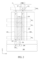
図2は、本発明のある実施形態による、活性円柱C1の垂直NORストリングの、グローバルビット線GBL1、グローバルソース線GSL1、および共通柱身バイアスソース206への接続を示す、Z-Y平面の断面図である。図2に示されているように、ビットラインアクセス選択トランジスタ211は、グローバルビット線GBL1とローカルビット線LBL1を接続し、コンタクト256は、任意選択で、活性帯状体上のP-柱身(または無ドープの柱身)領域を基板200内の柱身バイアスソース206に接続する。ビットラインアクセス選択トランジスタ211が活性円柱C1の上方に形成されている。しかしながら、代わりに、ビットラインアクセス選択トランジスタ211は、活性円柱C1の底部で、または他の実施形態の基板200内で形成され得る。
FIG. 2 shows ZY showing the connection of the vertical NOR string of active column C 1 to global bit line GBL 1 , global source line GSL 1 , and common
たとえば、ビットラインアクセス選択トランジスタ211は、N+/P-/N+ドープされた多結晶シリコンスタックの絶縁された島内に、アクセス選択ワード線SWLと共に、形成され得る。十分に高い電圧が選択ワード線SWLに印加された場合、P-チャネルが反転されて、それによりローカルビット線LBL1をグローバルビット線GBL1に接続する。アクセス選択ワード線SWLは、垂直NORストリングのTFT270への制御ゲートとして機能する、ワード線223と異なる方向(すなわち、Y方向)に沿って通り得る。アクセス選択ワード線SWLは、ワード線223から別に形成され得る。ある実施形態では、グローバルビット線GBL1は、水平にX方向(すなわち、ワード線の方向と垂直に)に沿って通り、ビットラインアクセス選択トランジスタ211は、グローバルビット線GBL1によってサービングされる多くの垂直NORストリングのうちの単に1つのローカルビット線である、ローカルビット線LBL1へのアクセスを提供する。読み出しおよびプログラム動作の効率を向上させるために、マルチゲートNORストリングアレイでは、数千のグローバルビット線は、アクセス選択ワード線SWLによってアクセスされる、数千の垂直NORストリングのローカルビット線に、並列にアクセスするために使用され得る。図2では、ローカルソース線LSL1が、コンタクト257を介してグローバルソース線GSL1に接続され得る。図2の活性円柱C1の垂直NORストリングは、図解目的だけのためのものであることが分かる。いくつかの他の実施形態では、ビットラインアクセス選択トランジスタ211は、省略され得ることが理解されよう。
For example, the bitline access
グローバルソース線GSL1は、基板200内のデコーディング回路によってデコードされ得る。支援回路は、とりわけ、アドレスエンコーダ、アドレスデコーダ、センス増幅器、入力/出力ドライバ、シフトレジスタ、ラッチ、基準セル、電力供給ライン、バイアスおよび基準電圧発生器、インバータ、NAND、NOR、排他的論理和および他のロジックゲート、他の記憶素子、シーケンサ、ならびに状態機械を備え得る。マルチゲートNORストリングアレイは、回路の複数のブロックとして組織され得、各ブロックは、複数のマルチゲートNORストリングアレイを有する。
Global source line GSL 1 may be decoded by decoding circuitry in
図3は、本発明の実施形態による、ワード線スタックを共有する垂直NORストリングの互い違いの近接実装を示す、X-Y平面の断面図である。本発明のある実施形態によれば、図3で示されているように、複数の垂直NORストリングまたは周りを覆うワード線を備える活性円柱が、図示されている。垂直NORストリングまたは活性円柱は、共により近接するように互い違いにされ、その結果、ワード線スタック323p(WL31-0)は、より多くの垂直NORストリングによって共有され得る。
FIG. 3 is a cross-sectional view in the XY plane showing a staggered close-in implementation of vertical NOR strings sharing a wordline stack, according to an embodiment of the present invention. According to one embodiment of the present invention, as shown in FIG. 3, an active column with multiple vertical NOR strings or word lines wrapped around is illustrated. The vertical NOR strings or active columns are staggered closer together so that
図3では、半導体材料の複数の活性円柱(チャネルホールCH00、CH01、CH10、CH11によって表される)が、基板(図3に図示せず)上方に配置されており、複数の活性円柱の各々は、基板の平坦面に直交する方向に沿って延在する。活性円柱は、2次元のアレイに互い違いに配設されている。垂直NORストリングは、チャネルホールCH00、CH01、CH10、CH11、それぞれの内側に形成されている。チャネルホールCH00、CH01、CH10、CH11は、ワード線間の金属ワード線のスタックと誘電体絶縁層をエッチングで貫通することによって形成される。製造工程フローは、従来技術の垂直NANDストリングのものと同様であるが、垂直NANDウイング内のトランジスタが直列に配設されているのに対して、垂直NORストリング内のトランジスタが互いに平行に配設されていることを除く。4つの例示のチャネルホールCH00、CH01、CH10、CH11の各々の内部で、垂直NORストリングのトランジスタ形成は、垂直NORストリングに沿ったすべてのTFTの1つの共有ローカルソース線(LSL)355ならびに2つのローカルビット線(LBL)354aおよび354bを備える、チャネルホールの深さ全体に延在するN+ドープ垂直柱によって支援される。 In FIG. 3, a plurality of active columns of semiconductor material (represented by channel holes CH 00 , CH 01 , CH 10 , CH 11 ) are positioned above a substrate (not shown in FIG. 3) and a plurality of Each of the active columns extends along a direction perpendicular to the planar surface of the substrate. The active columns are staggered in a two-dimensional array. A vertical NOR string is formed inside each of the channel holes CH 00 , CH 01 , CH 10 , CH 11 . Channel holes CH 00 , CH 01 , CH 10 , CH 11 are formed by etching through the stack of metal wordlines and the dielectric insulating layer between the wordlines. The fabrication process flow is similar to that of prior art vertical NAND strings, except that the transistors in the vertical NAND wings are arranged in series while the transistors in the vertical NOR strings are arranged parallel to each other. Except that Inside each of the four exemplary channel holes CH 00 , CH 01 , CH 10 , CH 11 , the transistor formation of the vertical NOR string is one shared local source line (LSL) for all TFTs along the vertical NOR string. Aided by N + doped vertical pillars extending the entire depth of the channel hole, comprising 355 and two local bit lines (LBLs) 354a and 354b.
本発明のある実施形態によれば、4つの例示のチャネルホールCH00、CH01、CH10、CH11の各々において、無ドープのまたは低濃度ドープのチャネル領域356aおよび356bは、ローカルビット線(LBL)354aおよび354bにそれぞれ隣接して配置されている。チャネル領域356aおよび356bは、絶縁層などのチャネルブレーカ320によって、互いから分離されている。電荷捕捉層を含む電荷蓄積素子334は、チャネル領域356aおよび356bとワード線スタック323pとの間に位置しており、そのため、垂直活性帯状体に沿った2、4、8、16、32、64、128またはより多くのTFTのスタックを形成する。本発明のある実施形態によれば、電荷蓄積素子334の電荷捕捉層は、それに限定されないが、窒化シリコンを含み得る。電荷トラッピング層は、たとえば、トンネル誘電体(例えば、シリコン二酸化物)の薄膜と、その後に続く窒化シリコンまたは非導電性誘電体材料に埋め込まれた導電性ナノドットなどの電荷トラッピング材料の薄層と、または絶縁フローディングゲート、から構成されるトランジスタゲート誘電体材料であり得、ONO(酸化物-窒化物-酸化物)などの阻止誘電体層またはアルミニウム酸化物もしくはハフニウム酸化物などの高誘電率膜、あるいはそのような誘電体のいくつかの組み合わせによって覆われている。電荷は、チャネルホットエレクトロン注入プログラミング手法を使用して、電荷捕捉層内に蓄積される。
In each of the four exemplary channel holes CH 00 , CH 01 , CH 10 , CH 11 , undoped or lightly doped
図3の実施形態では、ワード線スタックは、エアギャップまたは絶縁分離310によって互いから分離されている個々の水平帯状体323p(WL31-0)、323p(WL31-1)と共に、Y方向に通っている。8つの例示のグローバルビット線(GBL)314-0~314-7は、ワード線と垂直に、X方向に沿った列で水平に通っている。8つの例示のグローバルビット線(GBL)314-0~314-7の各々は、垂直帯状体の列に沿ったローカルビット線(LBL)に、メモリアレイ上方に位置し得るアクセス選択トランジスタ(図2の211、図3で図示せず)を介してアクセスする。同様に、各グローバルソース線(図3で図示せず)は、列にそったローカルソース線柱にアクセスする。たとえば、グローバルソース線は、メモリアレイの下方に配置され得る。
In the embodiment of FIG. 3, the word line stack runs through in the Y direction with individual
図3では、2つのTFT(または2つのメモリセル)が4つの例示のチャネルホールCH00、CH01、CH10、CH11の各々に配置されている。たとえば、2つのメモリセルT10aおよびT10bは、チャネルホールCH10内に配置され、2つのメモリセルT00aおよびT00bは、チャネルホールCH00内に配置され、2つのメモリセルT11aおよびT11bは、チャネルホールCH11内に配置され、2つのメモリセルT01aおよびT01bは、チャネルホールCH01内に配置されている。図3に示されている、各垂直NORストリングは、2つのチャネル領域356aおよび356b、2つのローカルビット線(LBL)354aおよび354b、ならびに1つの共有ローカルソース線(LSL)355を有する。たとえば、チャネル領域356a、ローカルビット線354a、共有ローカルソース線355、電荷蓄積要素334、およびワード線323pが、チャネルホールCH10内のメモリセルT10aを構成する。たとえば、チャネル領域356b、ローカルビット線354b、共有ローカルソース線355、電荷蓄積要素334、およびワード線323pが、チャネルホールCH10内のメモリセルT10bを構成する。したがって、開示されているメモリ構造は、垂直NORストリングの記憶密度を2倍にする。
In FIG. 3, two TFTs (or two memory cells) are placed in each of four exemplary channel holes CH00 , CH01 , CH10 , CH11 . For example, two memory cells T10a and T10b are arranged in the channel hole CH10 , two memory cells T00a and T00b are arranged in the channel hole CH00 , and two memory cells T11a and T11a and T00b are arranged in the channel hole CH00. 11b is arranged in channel hole CH11 , and two memory cells T01a and T01b are arranged in channel hole CH01 . Each vertical NOR string, shown in FIG. For example,
図4は、本発明の別の実施形態による、1つの活性円柱の複数のローカルビット線および複数のローカルソース線を示す、X-Y平面の概略断面図であり、同様の数字が、同様の要素、領域、または層を指定している。図4で示しているように、活性円柱ACが、ワード線WLによって、周りを覆われている。活性円柱ACは、基板(図4で図示せず)の平坦面に直交するZ方向に沿って延在する垂直NORストリングを備える。図3に示されているように、基板上で2次元アレイ内に互い違いに配置された複数の活性円柱が存在し得る。 FIG. 4 is a schematic cross-sectional view in the XY plane showing multiple local bit lines and multiple local source lines of one active column according to another embodiment of the present invention, where like numerals indicate like Specifies an element, region, or layer. As shown in FIG. 4, the active columns AC are surrounded by word lines WL. The active columns AC comprise vertical NOR strings extending along the Z-direction orthogonal to the planar surface of the substrate (not shown in FIG. 4). As shown in FIG. 3, there may be a plurality of active columns staggered in a two-dimensional array on the substrate.
活性円柱AC内の垂直NORストリングの1つの特定の平面のみが、図4に示されていることが分かる。環状シリコンチャネル356が、示されている。電荷捕捉層を含む電荷蓄積要素334が、シリコンチャネル356とワード線WLとの間に位置している。シリコンチャネル356および活性円柱ACの形状は、図解目的のためだけのものであることが理解されよう。卵形の形状、長方形の形状、または不規則な形状などの他の形状が、本発明の多様な実施形態に従って、適用可能であり得る。信号ラインLBLおよびLSLならびにチャネルブレーカの位置の形状は、図解目的のためだけのものであることが理解されよう。信号ラインLBLおよびLSLならびにチャネルブレーカの位置は、処理/製造要件に従って、調整され得る。
It can be seen that only one particular plane of vertical NOR strings within the active column AC is shown in FIG. An
別の実施形態によれば、活性円柱ACは、2つのローカルビット線354aおよび354b、ならびに2つのローカルソース線355aおよび355bを含み得る。チャネル領域356aは、ローカルビット線354aとローカルソース線355aとの間に位置する。チャネル領域356bは、ローカルビット線354bとローカルソース線355bとの間に位置する。同様に、絶縁層などのチャネルブレーカ320は、チャネル領域356aをチャネル領域356bから分離するように、2つのローカルビット線354aと354bとの間に位置する。いくつかの実施形態では、チャネルブレーカ320が省略され得ることが分かる。たとえば、チャネル領域356a、ローカルビット線354a、ローカルソース線355a、電荷蓄積要素334、およびワード線323pが、メモリセルT1を構成する。たとえば、チャネル領域356b、ローカルビット線354b、ローカルソース線355b、電荷蓄積要素334、およびワード線323pが、メモリセルT2を構成する。
According to another embodiment, active column AC may include two
各活性円柱内の信号ラインLBLおよびLSLの数は、設計要件に依存し得る。いくつかの実施形態では、3つ以上の信号ラインLBLおよび3つ以上の信号ラインLSLが、フラッシュメモリデバイスの記憶密度をさらに増大させるために、存在し得る。図5は、本発明のやはり別の実施形態による、1つの活性円柱の複数のローカルビット線および複数のローカルソース線を示す、X-Y平面の概略断面図であり、同様の数字が、同様の要素、領域、または層を指定している。図5で示しているように、同様に、活性円柱ACが、ワード線WLによって、周りを覆われている。活性円柱ACは、基板(図5で図示せず)の平坦面に直交するZ方向に沿って延在する垂直NORストリングを備える。 The number of signal lines LBL and LSL in each active column may depend on design requirements. In some embodiments, three or more signal lines LBL and three or more signal lines LSL may be present to further increase the storage density of flash memory devices. FIG. 5 is a schematic cross-sectional view in the XY plane showing multiple local bit lines and multiple local source lines of one active column, like numerals denoting like digits, according to yet another embodiment of the present invention. specifies an element, region, or layer of As shown in FIG. 5, the active columns AC are likewise surrounded by word lines WL. The active columns AC comprise vertical NOR strings extending along the Z-direction orthogonal to the planar surface of the substrate (not shown in FIG. 5).
活性円柱AC内の垂直NORストリングの1つの特定の平面のみが、図5に示されていることが分かる。環状シリコンチャネル356が、示されている。電荷捕捉層を含む電荷蓄積要素334が、シリコンチャネル356とワード線WLとの間に位置している。シリコンチャネル356および活性円柱ACの形状は、図解目的のためだけのものであることが理解されよう。卵形の形状、長方形の形状、または不規則な形状などの他の形状が、本発明の多様な実施形態に従って、適用可能であり得る。信号ラインLBLおよびLSLの位置の形状は、図解目的のためだけのものであることが理解されよう。信号ラインLBLおよびLSLの位置は、処理/製造要件に従って、調整され得る。
It can be seen that only one particular plane of vertical NOR strings within the active column AC is shown in FIG. An
別の実施形態によれば、活性円柱ACは、4つのローカルビット線354a~354d、ならびに4つのローカルソース線355a~355dを含み得る。シリコンチャネル356は、4つのローカルビット線354a~354d、ならびに4つのローカルソース線355a~355dによって、複数のチャネル領域356-1~356-8に分断されている。図5では、チャネルブレーカは、ローカルビット線間に配置されていない。複数のメモリセルが、フラッシュメモリデバイスの記憶密度を増大させるように、形成され得る。たとえば、チャネル領域356-1および356-8、ローカルビット線354a、ローカルビット線354aに隣接する2つのローカルソース線355aおよび355d、電荷蓄積要素334、ならびにワード線323pが、1つのメモリセルを構成する。
According to another embodiment, active column AC may include four
図6は、本発明のさらに別の実施形態による、1つの活性円柱の複数のローカルビット線および複数のローカルソース線を示す、X-Y平面の概略断面図であり、同様の数字が、同様の要素、領域、または層を指定している。図6で示しているように、同様に、活性円柱ACが、ワード線WLによって、周りを覆われている。活性円柱ACは、基板(図6で図示せず)の平坦面に直交するZ方向に沿って延在する垂直NORストリングを備える。 FIG. 6 is a schematic cross-sectional view in the XY plane showing multiple local bit lines and multiple local source lines of one active column according to yet another embodiment of the present invention, like numerals denoting like specifies an element, region, or layer of As shown in FIG. 6, the active columns AC are likewise surrounded by word lines WL. The active columns AC comprise vertical NOR strings extending along the Z-direction orthogonal to the planar surface of the substrate (not shown in FIG. 6).
活性円柱AC内の垂直NORストリングの1つの特定の平面のみが、図6に示されていることが分かる。環状シリコンチャネル356が、示されている。電荷捕捉層を含む電荷蓄積要素334が、シリコンチャネル356とワード線WLとの間に位置している。シリコンチャネル356および活性円柱ACの形状は、図解目的のためだけのものであることが理解されよう。卵形の形状、長方形の形状、または不規則な形状などの他の形状が、本発明の多様な実施形態に従って、適用可能であり得る。信号ラインLBLおよびLSLならびにチャネルブレーカの位置の形状は、図解目的のためだけのものであることが理解されよう。信号ラインLBLおよびLSLならびにチャネルブレーカの位置は、処理/製造要件に従って、調整され得る。
It can be seen that only one particular plane of vertical NOR strings within the active column AC is shown in FIG. An
別の実施形態によれば、活性円柱ACは、4つのローカルビット線354a~354d、ならびに4つのローカルソース線355a~355dを含み得る。シリコンチャネル356は、4つのローカルビット線354a~354d、ならびに4つのローカルソース線355a~355dによって、複数のチャネル領域356-1~356-6に分断されている。複数のメモリセルが、フラッシュメモリデバイスの記憶密度を増大させるように、形成され得る。たとえば、チャネル領域356-1、ローカルビット線354a、ローカルビット線354aに隣接する共有ローカルソース線355a、電荷蓄積要素334、ならびにワード線323pが、メモリセルT1を構成する。たとえば、チャネル領域356-2、ローカルビット線354b、ローカルビット線354bに隣接する共有ローカルソース線355a、電荷蓄積要素334、ならびにワード線323pが、メモリセルT2を構成する。たとえば、チャネル領域356-3および356-4、ローカルビット線354c、ローカルビット線354cに隣接する2つのローカルソース線355bおよび355c、電荷蓄積要素334、ならびにワード線323pが、メモリセルT3を構成する。たとえば、チャネル領域356-5および356-6、ローカルビット線354d、ローカルビット線354dに隣接する2つのローカルソース線355cおよび355d、電荷蓄積要素334、ならびにワード線323pが、メモリセルT4を構成する。
According to another embodiment, active column AC may include four
図6では、2つの例示のチャネルブレーカ320aおよび320bが、チャネルを分断するために追加されているが、必ずしも有する必要はない。2つのチャネルブレーカ320aおよび320bは、図解目的のためだけのものであることが分かる。チャネルブレーカの数は、各LBLがそれに加えて少なくとも1つのLSL有することができ、LBLとLSLとの間に連続するチャネルが存在する、という事実に影響を及ぼさない限り、増減され得る。この図内のチャネルブレーカの位置および数は、図解のためだけのものである。本発明の教示を保持しながらも、デバイスおよび方法の多数の変形および変更がなされ得ることに、当業者は、容易に気づくであろう。したがって、上の開示は、添付の請求項の境界によってのみ、限定されると解釈されるべきである。
In FIG. 6, two
1 メモリ構造
10 基板
111 垂直NORストリング
112 グローバルソース線 (GSL)、信号ライン
113 ワード線(WL)
114 グローバルビット線(GBL)、信号ライン
200 基板
206 柱身バイアスソース
211 ビットラインアクセス選択トランジスタ
223 ワード線
256 コンタクト
257 コンタクト
270 垂直NORストリングのTFT
310 絶縁分離
314-0~314-7 グローバルビット線(GBL)
320、320a、320b チャネルブレーカ
323p ワード線スタック
334 電荷蓄積素子
354a~354d ローカルビット線(LBL)
355、355a~355d ローカルソース線(LSL)
356 チャネル領域、環状シリコンチャネル
356a、356b、356-1~356-8 チャネル領域
1
114 global bit line (GBL),
310 isolation 314-0 to 314-7 global bit line (GBL)
320, 320a,
355, 355a-355d Local source line (LSL)
356 channel region,
Claims (16)
前記基板上方に配置された、垂直方向に沿って延在する半導体材料の円柱と、
前記円柱の周りを覆っているワード線スタックと、
前記ワード線スタックと前記円柱との間に配置された電荷蓄積要素と、を含み、前記円柱、前記電荷蓄積要素、および前記ワード線スタックは、少なくとも2つのメモリセルを構成する、3次元フラッシュメモリデバイスであって、
前記少なくとも2つのメモリセルのうちの2つは、前記垂直方向に沿って延在する共通のローカルソース線を含み、
前記少なくとも2つのメモリセルのうちの2つは、前記垂直方向に沿って延在し、前記少なくとも2つのメモリセルのうちの2つを分離する、チャネルブレーカを含み、
前記円柱は、前記垂直方向に沿って延在する、少なくとも2つのローカルビット線および前記共通のローカルソース線を備え、
前記3次元フラッシュメモリデバイスは、
前記少なくとも2つのローカルビット線のうちの第1のローカルビット線と、前記共通のローカルソース線との間の第1のチャネル領域と、
前記少なくとも2つのローカルビット線のうちの第2のローカルビット線と、前記共通のローカルソース線との間の第2のチャネル領域と、を含み、
前記チャネルブレーカは、前記第1のチャネル領域を前記第2のチャネル領域から分離する、
3次元フラッシュメモリデバイス。 a substrate;
a column of semiconductor material disposed above the substrate and extending along a vertical direction;
a word line stack wrapped around the cylinder;
a charge storage element disposed between the word line stack and the cylinder, wherein the cylinder, the charge storage element, and the word line stack constitute at least two memory cells. a device,
two of the at least two memory cells including a common local source line extending along the vertical direction;
two of the at least two memory cells including channel breakers extending along the vertical direction and separating two of the at least two memory cells;
said cylinder comprises at least two local bit lines and said common local source line extending along said vertical direction;
The three-dimensional flash memory device comprises:
a first channel region between a first local bit line of the at least two local bit lines and the common local source line;
a second local bit line of the at least two local bit lines and a second channel region between the common local source line;
the channel breaker separates the first channel region from the second channel region;
3D flash memory device.
前記基板上方に配置された半導体材料の複数の円柱であって、前記複数の円柱の各々が、垂直方向に沿って延在する、複数の円柱と、
前記複数の円柱の周りを覆っているワード線スタックと、
前記ワード線スタックと前記複数の円柱の各々との間に配置された電荷蓄積要素と、を含み、前記複数の円柱の各々、前記電荷蓄積要素、および前記ワード線スタックは、複数のメモリセルを構成し、
前記複数のメモリセルは、前記垂直方向に沿って延在する少なくとも1つの共通のローカルソース線を含み、
前記複数の円柱の各々は、前記垂直方向に沿って延在する、複数のローカルビット線および複数のローカルソース線を備え、複数のチャネル領域が、前記複数のローカルビット線と複数のローカルソース線との間に配置されており、
前記複数のチャネル領域のうちの2つの間を分離するチャネルブレーカをさらに備える、
3次元フラッシュメモリデバイス。 a substrate;
a plurality of cylinders of semiconductor material disposed above the substrate, each cylinder extending along a vertical direction;
a word line stack wrapped around the plurality of columns;
a charge storage element disposed between the word line stack and each of the plurality of columns, wherein each of the plurality of columns, the charge storage element, and the word line stack define a plurality of memory cells. compose and
the plurality of memory cells including at least one common local source line extending along the vertical direction;
each of the plurality of cylinders includes a plurality of local bit lines and a plurality of local source lines extending along the vertical direction, and the plurality of channel regions comprises the plurality of local bit lines and the plurality of local source lines; is placed between
further comprising a channel breaker separating between two of the plurality of channel regions;
3D flash memory device.
Applications Claiming Priority (1)
| Application Number | Priority Date | Filing Date | Title |
|---|---|---|---|
| PCT/CN2019/093678 WO2020258246A1 (en) | 2019-06-28 | 2019-06-28 | Three-dimensional flash memory device with increased storage density |
Publications (2)
| Publication Number | Publication Date |
|---|---|
| JP2022538095A JP2022538095A (en) | 2022-08-31 |
| JP7325552B2 true JP7325552B2 (en) | 2023-08-14 |
Family
ID=68634396
Family Applications (1)
| Application Number | Title | Priority Date | Filing Date |
|---|---|---|---|
| JP2021576379A Active JP7325552B2 (en) | 2019-06-28 | 2019-06-28 | High storage density 3D flash memory device |
Country Status (7)
| Country | Link |
|---|---|
| US (2) | US11211400B2 (en) |
| EP (1) | EP3963628B1 (en) |
| JP (1) | JP7325552B2 (en) |
| KR (1) | KR102672972B1 (en) |
| CN (2) | CN110520990B (en) |
| TW (1) | TWI725648B (en) |
| WO (1) | WO2020258246A1 (en) |
Families Citing this family (21)
| Publication number | Priority date | Publication date | Assignee | Title |
|---|---|---|---|---|
| TWI848993B (en) * | 2018-10-26 | 2024-07-21 | 美商蘭姆研究公司 | Self-aligned vertical integration of three-terminal memory devices |
| US11729988B2 (en) * | 2020-06-18 | 2023-08-15 | Taiwan Semiconductor Manufacturing Company, Ltd. | Memory device comprising conductive pillars and method of forming the same |
| WO2022006776A1 (en) * | 2020-07-08 | 2022-01-13 | Yangtze Memory Technologies Co., Ltd. | Three-dimensional memory devices with channel structures having plum blossom shape |
| CN112106199B (en) * | 2020-07-08 | 2024-04-16 | 长江存储科技有限责任公司 | Method for forming a three-dimensional memory device having a channel structure having a quincunx shape |
| WO2022082346A1 (en) | 2020-10-19 | 2022-04-28 | Yangtze Memory Technologies Co., Ltd. | Three-dimensional memory devices with channel structures having plum blossom shape |
| WO2022082347A1 (en) | 2020-10-19 | 2022-04-28 | Yangtze Memory Technologies Co., Ltd. | Three-dimensional memory devices with channel structures having plum blossom shape and methods for forming the same |
| CN117881189A (en) * | 2020-11-13 | 2024-04-12 | 武汉新芯集成电路制造有限公司 | Semiconductor device |
| TWI759015B (en) * | 2020-12-17 | 2022-03-21 | 旺宏電子股份有限公司 | Three-dimensional memory device and method for manufacturing the same |
| US11778823B2 (en) | 2020-12-17 | 2023-10-03 | Macronix International Co., Ltd. | Three-dimensional memory device and method for manufacturing the same |
| US11758735B2 (en) * | 2021-02-25 | 2023-09-12 | Taiwan Semiconductor Manufacturing Company, Ltd. | Common-connection method in 3D memory |
| US11980035B2 (en) * | 2021-03-04 | 2024-05-07 | Taiwan Semiconductor Manufacturing Company, Ltd. | Three-dimensional memory devices and methods of manufacturing thereof |
| TWI763361B (en) * | 2021-03-10 | 2022-05-01 | 旺宏電子股份有限公司 | Memory device and method for manufacturing the same and method for operating the same |
| US12262540B2 (en) * | 2021-04-08 | 2025-03-25 | Taiwan Semiconductor Manufacturing Company, Ltd. | Semiconductor memory devices and methods of manufacturing thereof |
| US11647637B2 (en) * | 2021-08-20 | 2023-05-09 | Taiwan Semiconductor Manufacturing Company, Ltd. | Semiconductor memory devices and methods of manufacturing thereof |
| US11903203B2 (en) * | 2021-08-30 | 2024-02-13 | Macronix International Co., Ltd. | 3D and flash memory device and method of fabricating the same |
| US20230106571A1 (en) * | 2021-10-06 | 2023-04-06 | Macronix International Co., Ltd. | 3d nor and 3d nand memory integration |
| US12142656B2 (en) * | 2021-12-03 | 2024-11-12 | International Business Machines Corporation | Staggered stacked semiconductor devices |
| KR20240122985A (en) * | 2023-02-06 | 2024-08-13 | 에스케이하이닉스 주식회사 | Semiconductor device and manufacturing method of semiconductor device |
| US20250006261A1 (en) * | 2023-06-27 | 2025-01-02 | Micron Technology, Inc. | Memory device with segmented sgd drain |
| TWI857842B (en) * | 2023-11-08 | 2024-10-01 | 旺宏電子股份有限公司 | 3d memory |
| US12406735B2 (en) * | 2023-11-08 | 2025-09-02 | Macronix International Co., Ltd. | 3D memory |
Citations (4)
| Publication number | Priority date | Publication date | Assignee | Title |
|---|---|---|---|---|
| US20160099254A1 (en) | 2014-10-03 | 2016-04-07 | Sandisk Technologies Inc. | Memory Hole Structure in Three Dimensional Memory |
| US20170148517A1 (en) | 2015-11-25 | 2017-05-25 | Eli Harari | Three-dimensional vertical nor flash thin film transistor strings |
| WO2017091338A1 (en) | 2015-11-25 | 2017-06-01 | Eli Harari | Three-dimensional vertical nor flash thin film transistor strings |
| US20180182776A1 (en) | 2016-12-22 | 2018-06-28 | Samsung Electronics Co., Ltd. | Vertical memory devices |
Family Cites Families (24)
| Publication number | Priority date | Publication date | Assignee | Title |
|---|---|---|---|---|
| TW406419B (en) * | 1998-01-15 | 2000-09-21 | Siemens Ag | Memory-cells arrangement and its production method |
| US6536719B2 (en) | 2001-07-17 | 2003-03-25 | .Engineering, Inc. | Single-handed cord/cable management device |
| TW569378B (en) | 2002-07-25 | 2004-01-01 | Taiwan Semiconductor Mfg | Structure with L-shape word line spacer and fabricating method thereof |
| KR100909627B1 (en) | 2007-10-10 | 2009-07-27 | 주식회사 하이닉스반도체 | Flash memory devices |
| KR101469106B1 (en) * | 2008-07-02 | 2014-12-05 | 삼성전자주식회사 | Three-dimensional semiconductor device, operation method and manufacturing method thereof |
| WO2012002186A1 (en) | 2010-07-02 | 2012-01-05 | Semiconductor Energy Laboratory Co., Ltd. | Semiconductor device |
| KR101780274B1 (en) * | 2011-05-04 | 2017-09-21 | 에스케이하이닉스 주식회사 | Nonvolatile memory device |
| US9147493B2 (en) * | 2013-06-17 | 2015-09-29 | Micron Technology, Inc. | Shielded vertically stacked data line architecture for memory |
| KR102128465B1 (en) * | 2014-01-03 | 2020-07-09 | 삼성전자주식회사 | Vertical structure non-volatile memory device |
| KR102145062B1 (en) * | 2014-03-17 | 2020-08-18 | 에스케이하이닉스 주식회사 | Semiconductor apparatus |
| US9666594B2 (en) * | 2014-09-05 | 2017-05-30 | Sandisk Technologies Llc | Multi-charge region memory cells for a vertical NAND device |
| US9418750B2 (en) * | 2014-09-15 | 2016-08-16 | Sandisk Technologies Llc | Single ended word line and bit line time constant measurement |
| US20170062456A1 (en) * | 2015-08-31 | 2017-03-02 | Cypress Semiconductor Corporation | Vertical division of three-dimensional memory device |
| US9858009B2 (en) | 2015-10-26 | 2018-01-02 | Sandisk Technologies Llc | Data folding in 3D nonvolatile memory |
| TWI572018B (en) | 2015-10-28 | 2017-02-21 | 旺宏電子股份有限公司 | Memory device and fabricating method thereof |
| US10103155B2 (en) * | 2016-03-09 | 2018-10-16 | Toshiba Memory Corporation | Semiconductor memory device |
| US9847342B2 (en) * | 2016-03-14 | 2017-12-19 | Toshiba Memory Corporation | Semiconductor memory device and method for manufacturing same |
| KR102637644B1 (en) * | 2016-07-14 | 2024-02-19 | 삼성전자주식회사 | Memory device |
| WO2018144957A1 (en) * | 2017-02-04 | 2018-08-09 | Monolithic 3D Inc. | 3d semiconductor device and structure |
| CN107527919A (en) * | 2017-08-31 | 2017-12-29 | 长江存储科技有限责任公司 | A kind of 3D nand memories part and its manufacture method |
| CN109698162A (en) * | 2017-10-20 | 2019-04-30 | 萨摩亚商费洛储存科技股份有限公司 | Three-dimensional memory element and method of manufacturing the same |
| CN107863348B (en) * | 2017-11-01 | 2019-03-12 | 长江存储科技有限责任公司 | A 3D NAND memory device and its manufacturing method |
| CN107994033B (en) * | 2017-11-16 | 2020-05-12 | 长江存储科技有限责任公司 | A 3D NAND channel hole forming method based on oxide-polysilicon thin film stacking |
| CN109801922B (en) * | 2019-01-31 | 2020-10-20 | 长江存储科技有限责任公司 | A method of forming a three-dimensional memory and a three-dimensional memory |
-
2019
- 2019-06-28 EP EP19935539.7A patent/EP3963628B1/en active Active
- 2019-06-28 CN CN201980001326.7A patent/CN110520990B/en active Active
- 2019-06-28 CN CN202010498902.8A patent/CN111613623B/en active Active
- 2019-06-28 WO PCT/CN2019/093678 patent/WO2020258246A1/en not_active Ceased
- 2019-06-28 KR KR1020217041725A patent/KR102672972B1/en active Active
- 2019-06-28 JP JP2021576379A patent/JP7325552B2/en active Active
- 2019-11-29 US US16/699,121 patent/US11211400B2/en active Active
- 2019-12-03 TW TW108144109A patent/TWI725648B/en active
-
2021
- 2021-10-13 US US17/500,370 patent/US11956962B2/en active Active
Patent Citations (5)
| Publication number | Priority date | Publication date | Assignee | Title |
|---|---|---|---|---|
| US20160099254A1 (en) | 2014-10-03 | 2016-04-07 | Sandisk Technologies Inc. | Memory Hole Structure in Three Dimensional Memory |
| US20170148517A1 (en) | 2015-11-25 | 2017-05-25 | Eli Harari | Three-dimensional vertical nor flash thin film transistor strings |
| WO2017091338A1 (en) | 2015-11-25 | 2017-06-01 | Eli Harari | Three-dimensional vertical nor flash thin film transistor strings |
| JP2019504479A (en) | 2015-11-25 | 2019-02-14 | サンライズ メモリー コーポレイション | 3D vertical NOR flash thin film transistor string |
| US20180182776A1 (en) | 2016-12-22 | 2018-06-28 | Samsung Electronics Co., Ltd. | Vertical memory devices |
Also Published As
| Publication number | Publication date |
|---|---|
| EP3963628A4 (en) | 2022-12-14 |
| CN111613623B (en) | 2021-02-19 |
| WO2020258246A1 (en) | 2020-12-30 |
| CN110520990B (en) | 2020-05-22 |
| EP3963628A1 (en) | 2022-03-09 |
| US11211400B2 (en) | 2021-12-28 |
| US11956962B2 (en) | 2024-04-09 |
| TW202101679A (en) | 2021-01-01 |
| JP2022538095A (en) | 2022-08-31 |
| TWI725648B (en) | 2021-04-21 |
| KR102672972B1 (en) | 2024-06-05 |
| EP3963628B1 (en) | 2023-12-06 |
| US20200411539A1 (en) | 2020-12-31 |
| CN110520990A (en) | 2019-11-29 |
| US20220045099A1 (en) | 2022-02-10 |
| KR20220010027A (en) | 2022-01-25 |
| CN111613623A (en) | 2020-09-01 |
Similar Documents
| Publication | Publication Date | Title |
|---|---|---|
| JP7325552B2 (en) | High storage density 3D flash memory device | |
| US10262739B2 (en) | Devices including memory arrays, row decoder circuitries and column decoder circuitries | |
| CN112420715A (en) | Multilayer memory device including under-array buffer circuitry | |
| US11011208B2 (en) | Semiconductor memory device including parallel substrates in three dimensional structures | |
| US11605588B2 (en) | Memory device including data lines on multiple device levels | |
| KR20100032211A (en) | Non-volatile memory devices and method of operating the same | |
| US20240420766A1 (en) | Memory device including in-tier driver circuit | |
| US11798631B2 (en) | Transfer latch tiers | |
| CN115623787A (en) | Integrated assembly and method of forming an integrated assembly | |
| US20250380420A1 (en) | Memory device including concentric conductive contacts | |
| US20250372168A1 (en) | Memory device including conductive contacts in treated tiers | |
| US12010847B2 (en) | Foundational supports within integrated assemblies | |
| US20260075829A1 (en) | Memory device including control gates having partial dielectric liners | |
| US20250378857A1 (en) | Memory device including conductive contacts and support structures | |
| US20250372169A1 (en) | Memory device including conductive contacts aligned with support structures | |
| US20260033318A1 (en) | Memory device including conductive contacts with multiple liners | |
| TW202608224A (en) | Memory device including conductive contacts in treated tiers | |
| TW202608223A (en) | Memory device including conductive contacts aligned with support structures | |
| TW202614775A (en) | Memory device including conductive contacts with multiple liners |
Legal Events
| Date | Code | Title | Description |
|---|---|---|---|
| A521 | Request for written amendment filed |
Free format text: JAPANESE INTERMEDIATE CODE: A523 Effective date: 20211221 |
|
| A621 | Written request for application examination |
Free format text: JAPANESE INTERMEDIATE CODE: A621 Effective date: 20211221 |
|
| A131 | Notification of reasons for refusal |
Free format text: JAPANESE INTERMEDIATE CODE: A131 Effective date: 20230110 |
|
| A521 | Request for written amendment filed |
Free format text: JAPANESE INTERMEDIATE CODE: A523 Effective date: 20230328 |
|
| TRDD | Decision of grant or rejection written | ||
| A01 | Written decision to grant a patent or to grant a registration (utility model) |
Free format text: JAPANESE INTERMEDIATE CODE: A01 Effective date: 20230703 |
|
| A61 | First payment of annual fees (during grant procedure) |
Free format text: JAPANESE INTERMEDIATE CODE: A61 Effective date: 20230801 |
|
| R150 | Certificate of patent or registration of utility model |
Ref document number: 7325552 Country of ref document: JP Free format text: JAPANESE INTERMEDIATE CODE: R150 |