JP6986397B2 - 基板処理装置、基板処理方法および記憶媒体 - Google Patents
基板処理装置、基板処理方法および記憶媒体 Download PDFInfo
- Publication number
- JP6986397B2 JP6986397B2 JP2017176844A JP2017176844A JP6986397B2 JP 6986397 B2 JP6986397 B2 JP 6986397B2 JP 2017176844 A JP2017176844 A JP 2017176844A JP 2017176844 A JP2017176844 A JP 2017176844A JP 6986397 B2 JP6986397 B2 JP 6986397B2
- Authority
- JP
- Japan
- Prior art keywords
- chemical solution
- substrate
- supply unit
- peripheral edge
- wafer
- Prior art date
- Legal status (The legal status is an assumption and is not a legal conclusion. Google has not performed a legal analysis and makes no representation as to the accuracy of the status listed.)
- Active
Links
Images


Classifications
-
- H—ELECTRICITY
- H10—SEMICONDUCTOR DEVICES; ELECTRIC SOLID-STATE DEVICES NOT OTHERWISE PROVIDED FOR
- H10P—GENERIC PROCESSES OR APPARATUS FOR THE MANUFACTURE OR TREATMENT OF DEVICES COVERED BY CLASS H10
- H10P72/00—Handling or holding of wafers, substrates or devices during manufacture or treatment thereof
- H10P72/04—Apparatus for manufacture or treatment
- H10P72/0402—Apparatus for fluid treatment
- H10P72/0418—Apparatus for fluid treatment for etching
- H10P72/0422—Apparatus for fluid treatment for etching for wet etching
-
- H—ELECTRICITY
- H10—SEMICONDUCTOR DEVICES; ELECTRIC SOLID-STATE DEVICES NOT OTHERWISE PROVIDED FOR
- H10P—GENERIC PROCESSES OR APPARATUS FOR THE MANUFACTURE OR TREATMENT OF DEVICES COVERED BY CLASS H10
- H10P72/00—Handling or holding of wafers, substrates or devices during manufacture or treatment thereof
- H10P72/04—Apparatus for manufacture or treatment
- H10P72/0402—Apparatus for fluid treatment
- H10P72/0418—Apparatus for fluid treatment for etching
-
- H—ELECTRICITY
- H10—SEMICONDUCTOR DEVICES; ELECTRIC SOLID-STATE DEVICES NOT OTHERWISE PROVIDED FOR
- H10P—GENERIC PROCESSES OR APPARATUS FOR THE MANUFACTURE OR TREATMENT OF DEVICES COVERED BY CLASS H10
- H10P50/00—Etching of wafers, substrates or parts of devices
- H10P50/60—Wet etching
- H10P50/64—Wet etching of semiconductor materials
- H10P50/642—Chemical etching
-
- H—ELECTRICITY
- H10—SEMICONDUCTOR DEVICES; ELECTRIC SOLID-STATE DEVICES NOT OTHERWISE PROVIDED FOR
- H10P—GENERIC PROCESSES OR APPARATUS FOR THE MANUFACTURE OR TREATMENT OF DEVICES COVERED BY CLASS H10
- H10P50/00—Etching of wafers, substrates or parts of devices
- H10P50/60—Wet etching
- H10P50/66—Wet etching of conductive or resistive materials
- H10P50/663—Wet etching of conductive or resistive materials by chemical means only
- H10P50/667—Wet etching of conductive or resistive materials by chemical means only by liquid etching only
-
- H—ELECTRICITY
- H10—SEMICONDUCTOR DEVICES; ELECTRIC SOLID-STATE DEVICES NOT OTHERWISE PROVIDED FOR
- H10P—GENERIC PROCESSES OR APPARATUS FOR THE MANUFACTURE OR TREATMENT OF DEVICES COVERED BY CLASS H10
- H10P72/00—Handling or holding of wafers, substrates or devices during manufacture or treatment thereof
- H10P72/04—Apparatus for manufacture or treatment
- H10P72/0402—Apparatus for fluid treatment
- H10P72/0406—Apparatus for fluid treatment for cleaning followed by drying, rinsing, stripping, blasting or the like
- H10P72/0411—Apparatus for fluid treatment for cleaning followed by drying, rinsing, stripping, blasting or the like for wet cleaning or washing
- H10P72/0414—Apparatus for fluid treatment for cleaning followed by drying, rinsing, stripping, blasting or the like for wet cleaning or washing using mainly spraying means, e.g. nozzles
-
- H—ELECTRICITY
- H10—SEMICONDUCTOR DEVICES; ELECTRIC SOLID-STATE DEVICES NOT OTHERWISE PROVIDED FOR
- H10P—GENERIC PROCESSES OR APPARATUS FOR THE MANUFACTURE OR TREATMENT OF DEVICES COVERED BY CLASS H10
- H10P72/00—Handling or holding of wafers, substrates or devices during manufacture or treatment thereof
- H10P72/04—Apparatus for manufacture or treatment
- H10P72/0402—Apparatus for fluid treatment
- H10P72/0418—Apparatus for fluid treatment for etching
- H10P72/0422—Apparatus for fluid treatment for etching for wet etching
- H10P72/0424—Apparatus for fluid treatment for etching for wet etching using mainly spraying means, e.g. nozzles
-
- H—ELECTRICITY
- H10—SEMICONDUCTOR DEVICES; ELECTRIC SOLID-STATE DEVICES NOT OTHERWISE PROVIDED FOR
- H10P—GENERIC PROCESSES OR APPARATUS FOR THE MANUFACTURE OR TREATMENT OF DEVICES COVERED BY CLASS H10
- H10P72/00—Handling or holding of wafers, substrates or devices during manufacture or treatment thereof
- H10P72/30—Handling or holding of wafers, substrates or devices during manufacture or treatment thereof for conveying, e.g. between different workstations
- H10P72/33—Handling or holding of wafers, substrates or devices during manufacture or treatment thereof for conveying, e.g. between different workstations into and out of processing chamber
-
- H—ELECTRICITY
- H10—SEMICONDUCTOR DEVICES; ELECTRIC SOLID-STATE DEVICES NOT OTHERWISE PROVIDED FOR
- H10P—GENERIC PROCESSES OR APPARATUS FOR THE MANUFACTURE OR TREATMENT OF DEVICES COVERED BY CLASS H10
- H10P72/00—Handling or holding of wafers, substrates or devices during manufacture or treatment thereof
- H10P72/70—Handling or holding of wafers, substrates or devices during manufacture or treatment thereof for supporting or gripping
- H10P72/76—Handling or holding of wafers, substrates or devices during manufacture or treatment thereof for supporting or gripping using mechanical means, e.g. clamps or pinches
- H10P72/7604—Handling or holding of wafers, substrates or devices during manufacture or treatment thereof for supporting or gripping using mechanical means, e.g. clamps or pinches the wafers being placed on a susceptor, stage or support
- H10P72/7618—Handling or holding of wafers, substrates or devices during manufacture or treatment thereof for supporting or gripping using mechanical means, e.g. clamps or pinches the wafers being placed on a susceptor, stage or support characterised by a movable susceptor, stage or support, others than those only rotating on their own vertical axis, e.g. susceptors on a rotating carrousel
-
- H—ELECTRICITY
- H10—SEMICONDUCTOR DEVICES; ELECTRIC SOLID-STATE DEVICES NOT OTHERWISE PROVIDED FOR
- H10P—GENERIC PROCESSES OR APPARATUS FOR THE MANUFACTURE OR TREATMENT OF DEVICES COVERED BY CLASS H10
- H10P72/00—Handling or holding of wafers, substrates or devices during manufacture or treatment thereof
- H10P72/70—Handling or holding of wafers, substrates or devices during manufacture or treatment thereof for supporting or gripping
- H10P72/76—Handling or holding of wafers, substrates or devices during manufacture or treatment thereof for supporting or gripping using mechanical means, e.g. clamps or pinches
- H10P72/7604—Handling or holding of wafers, substrates or devices during manufacture or treatment thereof for supporting or gripping using mechanical means, e.g. clamps or pinches the wafers being placed on a susceptor, stage or support
- H10P72/7624—Handling or holding of wafers, substrates or devices during manufacture or treatment thereof for supporting or gripping using mechanical means, e.g. clamps or pinches the wafers being placed on a susceptor, stage or support characterised by the mechanical construction of the susceptor, stage or support
-
- H—ELECTRICITY
- H10—SEMICONDUCTOR DEVICES; ELECTRIC SOLID-STATE DEVICES NOT OTHERWISE PROVIDED FOR
- H10P—GENERIC PROCESSES OR APPARATUS FOR THE MANUFACTURE OR TREATMENT OF DEVICES COVERED BY CLASS H10
- H10P74/00—Testing or measuring during manufacture or treatment of wafers, substrates or devices
- H10P74/27—Structural arrangements therefor
Landscapes
- Weting (AREA)
- Cleaning Or Drying Semiconductors (AREA)
- Chemical & Material Sciences (AREA)
- Chemical Kinetics & Catalysis (AREA)
- General Chemical & Material Sciences (AREA)
- Engineering & Computer Science (AREA)
- Manufacturing & Machinery (AREA)
Description
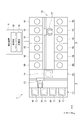
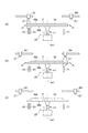
図1は、本実施形態に係る基板処理システムの概略構成を示す図である。以下では、位置関係を明確にするために、互いに直交するX軸、Y軸およびZ軸を規定し、Z軸正方向を鉛直上向き方向とする。図1に示すように、基板処理システム1は、搬入出ステーション2と、処理ステーション3とを備える。搬入出ステーション2と処理ステーション3とは隣接して設けられる。
続いて、基板処理システム1が含む基板処理装置10の構成を例示する。基板処理装置10は、表面にメタル膜等の被膜Fが形成されたウェハWを処理対象とし、被膜FのうちウェハWの周縁部(周縁Wcの近傍部分)に位置する部分を除去する処理を行う。被膜Fの一例としては、タングステンを含有しているタングステン膜が挙げられる。被膜Fの他の例としては、チタン膜、シリサイド膜、チタンオキサイド膜、チタンナイトライド膜、ルテニウム膜、金膜、プラチナ膜等が挙げられる。被膜Fは、多層膜(互いに組成の異なる複数の層を有する膜)であってもよい。
続いて、基板処理方法の一例として、基板処理装置10が実行する基板処理手順を説明する。この基板処理手順は、表面Waに被膜Fが形成されたウェハWを保持して回転させることと、ウェハWの表面Waの周縁部に第一薬液を供給することと、ウェハWの表面Waの周縁部に第一薬液が供給されているときに、ウェハWの裏面Wbの周縁部に第一薬液および第二薬液を供給することと、を含む。
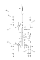
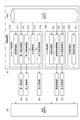
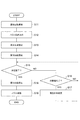
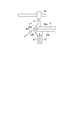
図5は、被膜Fが多層膜である場合のエッチング処理手順を例示するフローチャートである。図5に示すように、エッチング制御部110は、まずステップS11,S12,S13を順に実行する。ステップS11では、回転制御部111が、レシピ記憶部140に記憶されたエッチング処理用の回転速度ω1にてウェハWの回転を開始するように回転保持部20を制御する(図8の(a)参照)。ステップS12では、第一供給制御部112が、ノズル駆動部34によりノズル31をウェハWの表面Waの上方に配置するように第一供給部30を制御する。ステップS13では、比率調節部115が、レシピ記憶部140に記憶された被膜Fの種類の情報を参照し、処理対象の被膜の種類(被膜Fの最上層の種類)に応じて上記目標混合比率を設定する。たとえば比率調節部115は、ウェハWの周縁部の温度が、処理対象の被膜の処理に適した温度となるように、上記目標混合比率を設定する。なお、ステップS11,S12,S13の実行順序は適宜変更可能である。
図6に示すように、エッチング制御部110は、まずステップS31,S32,S33を順に実行する。ステップS31では、回転制御部121が、ウェハWの回転速度をレシピ記憶部140に記憶されたリンス処理用の回転速度ω2に変更するように回転保持部20を制御する(図8の(b)参照)。ステップS32では、第四供給制御部122が、ノズル駆動部64によりノズル61をウェハWの表面Waの上方に配置するように第四供給部60を制御する。ステップS33では、第四供給制御部122が、バルブ63を開いてノズル61からのリンス液の吐出を開始するように第四供給部60を制御する(図8の(b)参照)。なお、ステップS31,S32の実行順序は適宜変更可能である。
図7に示すように、乾燥制御部130は、ステップS41,S42,S43を順に実行する。ステップS41では、回転制御部131が、ウェハWの回転速度をレシピ記憶部140に記憶された乾燥処理用の回転速度ω3に変更するように回転保持部20を制御する(図8の(c)参照)。ステップS42では、回転制御部131が、レシピ記憶部140に記憶された上記乾燥時間の経過を待機する。ステップS43では、回転制御部131が、ウェハWの回転を停止させるように回転保持部20を制御する。以上で乾燥処理手順が完了する。
以上に説明したように、基板処理装置10は、表面Waに被膜Fが形成されたウェハWを保持して回転させる回転保持部20と、回転保持部20により保持されたウェハWの表面Waの周縁部に被膜Fのエッチング処理用の第一薬液を供給する第一供給部30と、ウェハWの裏面Wbの周縁部に第一薬液を供給する第二供給部40と、ウェハWの裏面Wbの周縁部に、第一薬液と発熱反応する第二薬液を供給する第三供給部50と、を備える。
Claims (10)
- 表面に被膜が形成された基板を保持して回転させる回転保持部と、
前記回転保持部により保持された前記基板の表面の周縁部に前記被膜のエッチング処理用の第一薬液を供給する第一供給部と、
前記基板の裏面の周縁部に前記第一薬液を供給する第二供給部と、
前記基板の裏面の周縁部に、前記第一薬液と発熱反応する第二薬液を供給する第三供給部と、
制御装置と、を備え、
前記制御装置は、
前記基板の表面の周縁部に前記第一薬液を供給するように前記第一供給部を制御することと、
前記基板の表面の周縁部に前記第一薬液が供給されているときに、当該基板の裏面の周縁部に前記第一薬液を供給するように前記第二供給部を制御することと、
前記基板の表面の周縁部および裏面の周縁部に前記第一薬液が供給されているときに、当該基板の裏面の周縁部に前記第二薬液を供給するように第三供給部を制御することと、を実行するように構成されている基板処理装置。 - 前記第三供給部は、前記第二供給部からの前記第一薬液が前記基板に到達する位置よりも前記基板の回転中心寄りの位置に前記第二薬液を到達させるように構成されている、請求項1記載の基板処理装置。
- 前記制御装置は、前記基板の裏面に到達する前記第一薬液および前記第二薬液の比率を、処理対象の被膜の種類に応じて調節するように前記第二供給部および前記第三供給部を制御することを更に実行するように構成されている、請求項1または2記載の基板処理装置。
- 前記制御装置は、前記基板の裏面に到達する前記第一薬液および前記第二薬液の比率の目標値を、予め記憶されたテーブルを参照することにより、前記被膜の種類に応じて設定するように構成されている、請求項3記載の基板処理装置。
- 前記被膜は多層膜であり、
前記制御装置は、前記基板の裏面に到達する前記第一薬液および前記第二薬液の比率を、前記多層膜のいずれの層が処理対象であるかに応じて変更するように構成されている、請求項3または4記載の基板処理装置。 - 前記制御装置は、前記第二供給部から供給された前記第一薬液と前記第三供給部から供給された前記第二薬液との混合液が、前記基板の裏面の周縁部から前記基板の表面の周縁部へ回りこみ、前記第一供給部から供給された前記第一薬液と前記基板の表面の周縁部において衝突するように、前記第一供給部、前記第二供給部、および前記第三供給部を制御することを更に実行するように構成されている、請求項1〜5のいずれか一項記載の基板処理装置。
- 前記被膜はタングステンを含有しており、
前記第一薬液は過酸化水素を含有し、前記第二薬液は硫酸を含有している、請求項1〜6のいずれか一項記載の基板処理装置。 - 表面に被膜が形成された基板を保持して回転させることと、
前記基板の表面の周縁部に前記被膜のエッチング処理用の第一薬液を供給することと、
前記基板の表面の周縁部に前記第一薬液が供給されているときに、当該基板の裏面の周縁部に前記第一薬液および前記第一薬液と発熱反応する第二薬液を供給することと、を含む基板処理方法。 - 前記基板の裏面に到達する前記第一薬液および前記第二薬液の比率を、処理対象の被膜の種類に応じて調節することを更に含む、請求項8記載の基板処理方法。
- 請求項8または9記載の基板処理方法を装置に実行させるためのプログラムを記憶した、コンピュータ読み取り可能な記憶媒体。
Priority Applications (4)
| Application Number | Priority Date | Filing Date | Title |
|---|---|---|---|
| JP2017176844A JP6986397B2 (ja) | 2017-09-14 | 2017-09-14 | 基板処理装置、基板処理方法および記憶媒体 |
| KR1020180106111A KR102559412B1 (ko) | 2017-09-14 | 2018-09-05 | 기판 처리 장치, 기판 처리 방법 및 기억 매체 |
| US16/123,525 US10490424B2 (en) | 2017-09-14 | 2018-09-06 | Substrate processing apparatus, substrate processing method, and storage medium |
| CN201811073540.7A CN109509715B (zh) | 2017-09-14 | 2018-09-14 | 基片处理装置、基片处理方法和存储介质 |
Applications Claiming Priority (1)
| Application Number | Priority Date | Filing Date | Title |
|---|---|---|---|
| JP2017176844A JP6986397B2 (ja) | 2017-09-14 | 2017-09-14 | 基板処理装置、基板処理方法および記憶媒体 |
Publications (2)
| Publication Number | Publication Date |
|---|---|
| JP2019054093A JP2019054093A (ja) | 2019-04-04 |
| JP6986397B2 true JP6986397B2 (ja) | 2021-12-22 |
Family
ID=65631441
Family Applications (1)
| Application Number | Title | Priority Date | Filing Date |
|---|---|---|---|
| JP2017176844A Active JP6986397B2 (ja) | 2017-09-14 | 2017-09-14 | 基板処理装置、基板処理方法および記憶媒体 |
Country Status (4)
| Country | Link |
|---|---|
| US (1) | US10490424B2 (ja) |
| JP (1) | JP6986397B2 (ja) |
| KR (1) | KR102559412B1 (ja) |
| CN (1) | CN109509715B (ja) |
Families Citing this family (6)
| Publication number | Priority date | Publication date | Assignee | Title |
|---|---|---|---|---|
| JP7241589B2 (ja) * | 2019-04-04 | 2023-03-17 | 東京エレクトロン株式会社 | 基板処理方法および基板処理装置 |
| CN110600403B (zh) * | 2019-08-27 | 2022-02-08 | 长江存储科技有限责任公司 | 一种晶片刻蚀装置 |
| JP7285741B2 (ja) * | 2019-08-30 | 2023-06-02 | 株式会社Screenホールディングス | 基板処理方法および基板処理装置 |
| JP7471170B2 (ja) * | 2020-08-03 | 2024-04-19 | 東京エレクトロン株式会社 | 基板処理方法、及び基板処理装置 |
| TWI888680B (zh) * | 2020-12-18 | 2025-07-01 | 日商東京威力科創股份有限公司 | 基板處理方法及基板處理裝置 |
| JP7774638B2 (ja) * | 2021-11-04 | 2025-11-21 | 東京エレクトロン株式会社 | 基板処理方法および基板処理装置 |
Family Cites Families (12)
| Publication number | Priority date | Publication date | Assignee | Title |
|---|---|---|---|---|
| JPS6291098A (ja) * | 1985-10-16 | 1987-04-25 | Foster Denki Kk | 電気音響変換器用振動板及びその製造方法 |
| JP3277404B2 (ja) * | 1993-03-31 | 2002-04-22 | ソニー株式会社 | 基板洗浄方法及び基板洗浄装置 |
| US6565928B2 (en) * | 1999-03-08 | 2003-05-20 | Tokyo Electron Limited | Film forming method and film forming apparatus |
| JP2005191511A (ja) * | 2003-12-02 | 2005-07-14 | Dainippon Screen Mfg Co Ltd | 基板処理装置および基板処理方法 |
| JP4906559B2 (ja) * | 2007-03-29 | 2012-03-28 | 大日本スクリーン製造株式会社 | 基板処理装置および基板処理方法 |
| JP5996381B2 (ja) * | 2011-12-28 | 2016-09-21 | 東京エレクトロン株式会社 | 基板処理装置および基板処理方法 |
| JP5792094B2 (ja) * | 2012-02-24 | 2015-10-07 | 東京エレクトロン株式会社 | 液処理装置、液処理方法および液処理方法を実行するためのコンピュータプログラムが記録された記録媒体 |
| JP5917346B2 (ja) * | 2012-09-07 | 2016-05-11 | 株式会社東芝 | エッチング方法、およびエッチング装置 |
| TWI630652B (zh) * | 2014-03-17 | 2018-07-21 | SCREEN Holdings Co., Ltd. | 基板處理裝置及使用基板處理裝置之基板處理方法 |
| JP6195803B2 (ja) * | 2014-05-02 | 2017-09-13 | 東京エレクトロン株式会社 | 基板処理装置、基板処理方法および記憶媒体 |
| JP6246749B2 (ja) * | 2015-01-28 | 2017-12-13 | 東京エレクトロン株式会社 | ウエットエッチング方法、基板液処理装置および記憶媒体 |
| JP6482978B2 (ja) * | 2015-07-23 | 2019-03-13 | 東京エレクトロン株式会社 | 基板処理装置 |
-
2017
- 2017-09-14 JP JP2017176844A patent/JP6986397B2/ja active Active
-
2018
- 2018-09-05 KR KR1020180106111A patent/KR102559412B1/ko active Active
- 2018-09-06 US US16/123,525 patent/US10490424B2/en active Active
- 2018-09-14 CN CN201811073540.7A patent/CN109509715B/zh active Active
Also Published As
| Publication number | Publication date |
|---|---|
| JP2019054093A (ja) | 2019-04-04 |
| US10490424B2 (en) | 2019-11-26 |
| CN109509715B (zh) | 2023-10-13 |
| KR102559412B1 (ko) | 2023-07-26 |
| KR20190030607A (ko) | 2019-03-22 |
| US20190080934A1 (en) | 2019-03-14 |
| CN109509715A (zh) | 2019-03-22 |
Similar Documents
| Publication | Publication Date | Title |
|---|---|---|
| JP6986397B2 (ja) | 基板処理装置、基板処理方法および記憶媒体 | |
| JP5712101B2 (ja) | 基板処理方法及び基板処理装置 | |
| US9255331B2 (en) | Apparatus for plating process | |
| US10185220B2 (en) | Substrate processing method, substrate processing apparatus, and non-transitory computer-readable medium | |
| JP7345401B2 (ja) | 基板処理方法および基板処理装置 | |
| JP2003318152A (ja) | 基板処理装置及び基板処理方法 | |
| JP4843043B2 (ja) | 基板処理装置及び基板処理方法 | |
| TWI576463B (zh) | A coating treatment device, a coating treatment method and a memory medium | |
| US7160416B2 (en) | Substrate treating apparatus | |
| JP2006344907A (ja) | 基板処理方法および基板処理装置 | |
| KR20070055346A (ko) | 액 처리 방법, 액 처리 장치 및 이를 행하는 제어프로그램이 기억된 컴퓨터 판독 가능한 기억 매체 | |
| JP7292120B2 (ja) | 基板処理方法および基板処理装置 | |
| JP7241594B2 (ja) | 基板処理方法および基板処理装置 | |
| JP2020170801A (ja) | 基板処理方法および基板処理装置 | |
| JP7693004B2 (ja) | 基板処理方法および基板処理装置 | |
| JP4680044B2 (ja) | 液処理方法、液処理装置、制御プログラム、およびコンピュータ読取可能な記憶媒体 | |
| WO2013002096A1 (ja) | めっき処理方法、めっき処理装置および記憶媒体 | |
| JP2007234812A (ja) | 基板処理方法および基板処理装置 | |
| JP6513492B2 (ja) | 基板処理方法、基板処理装置及び記憶媒体 | |
| JP7542078B2 (ja) | 基板処理装置、基板処理方法及びコンピュータ読み取り可能な記録媒体 | |
| JP2004356379A (ja) | 基板処理装置 |
Legal Events
| Date | Code | Title | Description |
|---|---|---|---|
| A621 | Written request for application examination |
Free format text: JAPANESE INTERMEDIATE CODE: A621 Effective date: 20200703 |
|
| A131 | Notification of reasons for refusal |
Free format text: JAPANESE INTERMEDIATE CODE: A131 Effective date: 20210601 |
|
| A977 | Report on retrieval |
Free format text: JAPANESE INTERMEDIATE CODE: A971007 Effective date: 20210531 |
|
| A521 | Request for written amendment filed |
Free format text: JAPANESE INTERMEDIATE CODE: A523 Effective date: 20210727 |
|
| TRDD | Decision of grant or rejection written | ||
| A01 | Written decision to grant a patent or to grant a registration (utility model) |
Free format text: JAPANESE INTERMEDIATE CODE: A01 Effective date: 20211102 |
|
| A61 | First payment of annual fees (during grant procedure) |
Free format text: JAPANESE INTERMEDIATE CODE: A61 Effective date: 20211129 |
|
| R150 | Certificate of patent or registration of utility model |
Ref document number: 6986397 Country of ref document: JP Free format text: JAPANESE INTERMEDIATE CODE: R150 |
|
| R250 | Receipt of annual fees |
Free format text: JAPANESE INTERMEDIATE CODE: R250 |
|
| R250 | Receipt of annual fees |
Free format text: JAPANESE INTERMEDIATE CODE: R250 |