JP6878338B2 - 受光装置および受光装置の製造方法 - Google Patents
受光装置および受光装置の製造方法 Download PDFInfo
- Publication number
- JP6878338B2 JP6878338B2 JP2018046725A JP2018046725A JP6878338B2 JP 6878338 B2 JP6878338 B2 JP 6878338B2 JP 2018046725 A JP2018046725 A JP 2018046725A JP 2018046725 A JP2018046725 A JP 2018046725A JP 6878338 B2 JP6878338 B2 JP 6878338B2
- Authority
- JP
- Japan
- Prior art keywords
- semiconductor layer
- light receiving
- type
- receiving device
- epitaxial layer
- Prior art date
- Legal status (The legal status is an assumption and is not a legal conclusion. Google has not performed a legal analysis and makes no representation as to the accuracy of the status listed.)
- Active
Links
- 238000004519 manufacturing process Methods 0.000 title claims description 8
- 238000006243 chemical reaction Methods 0.000 claims description 47
- 239000004065 semiconductor Substances 0.000 claims description 46
- 239000000758 substrate Substances 0.000 claims description 26
- 239000012535 impurity Substances 0.000 claims description 23
- 238000000034 method Methods 0.000 claims description 13
- 230000015572 biosynthetic process Effects 0.000 claims 2
- XUIMIQQOPSSXEZ-UHFFFAOYSA-N Silicon Chemical compound [Si] XUIMIQQOPSSXEZ-UHFFFAOYSA-N 0.000 description 18
- 229910052710 silicon Inorganic materials 0.000 description 18
- 239000010703 silicon Substances 0.000 description 18
- 230000001681 protective effect Effects 0.000 description 15
- 238000000926 separation method Methods 0.000 description 15
- 238000010791 quenching Methods 0.000 description 13
- 230000000171 quenching effect Effects 0.000 description 13
- 230000000052 comparative effect Effects 0.000 description 9
- 229910052751 metal Inorganic materials 0.000 description 9
- 239000002184 metal Substances 0.000 description 9
- 230000035945 sensitivity Effects 0.000 description 9
- 238000000098 azimuthal photoelectron diffraction Methods 0.000 description 7
- VYPSYNLAJGMNEJ-UHFFFAOYSA-N Silicium dioxide Chemical compound O=[Si]=O VYPSYNLAJGMNEJ-UHFFFAOYSA-N 0.000 description 6
- 238000010586 diagram Methods 0.000 description 6
- 229910052814 silicon oxide Inorganic materials 0.000 description 6
- 238000005229 chemical vapour deposition Methods 0.000 description 3
- 239000012528 membrane Substances 0.000 description 3
- 230000000694 effects Effects 0.000 description 2
- 230000005684 electric field Effects 0.000 description 2
- 239000007789 gas Substances 0.000 description 2
- 238000005468 ion implantation Methods 0.000 description 2
- 238000001020 plasma etching Methods 0.000 description 2
- 229910021420 polycrystalline silicon Inorganic materials 0.000 description 2
- RYGMFSIKBFXOCR-UHFFFAOYSA-N Copper Chemical compound [Cu] RYGMFSIKBFXOCR-UHFFFAOYSA-N 0.000 description 1
- VEXZGXHMUGYJMC-UHFFFAOYSA-N Hydrochloric acid Chemical compound Cl VEXZGXHMUGYJMC-UHFFFAOYSA-N 0.000 description 1
- 229910052782 aluminium Inorganic materials 0.000 description 1
- XAGFODPZIPBFFR-UHFFFAOYSA-N aluminium Chemical compound [Al] XAGFODPZIPBFFR-UHFFFAOYSA-N 0.000 description 1
- 229910052785 arsenic Inorganic materials 0.000 description 1
- 230000002238 attenuated effect Effects 0.000 description 1
- 239000012159 carrier gas Substances 0.000 description 1
- 230000015556 catabolic process Effects 0.000 description 1
- 239000004020 conductor Substances 0.000 description 1
- 229910052802 copper Inorganic materials 0.000 description 1
- 239000010949 copper Substances 0.000 description 1
- 239000013078 crystal Substances 0.000 description 1
- 230000002542 deteriorative effect Effects 0.000 description 1
- ZOCHARZZJNPSEU-UHFFFAOYSA-N diboron Chemical compound B#B ZOCHARZZJNPSEU-UHFFFAOYSA-N 0.000 description 1
- BUMGIEFFCMBQDG-UHFFFAOYSA-N dichlorosilicon Chemical compound Cl[Si]Cl BUMGIEFFCMBQDG-UHFFFAOYSA-N 0.000 description 1
- 238000005530 etching Methods 0.000 description 1
- PCHJSUWPFVWCPO-UHFFFAOYSA-N gold Chemical compound [Au] PCHJSUWPFVWCPO-UHFFFAOYSA-N 0.000 description 1
- 229910052737 gold Inorganic materials 0.000 description 1
- 239000010931 gold Substances 0.000 description 1
- 229910052739 hydrogen Inorganic materials 0.000 description 1
- 239000001257 hydrogen Substances 0.000 description 1
- 125000004435 hydrogen atom Chemical class [H]* 0.000 description 1
- 238000009413 insulation Methods 0.000 description 1
- 238000001459 lithography Methods 0.000 description 1
- 239000000463 material Substances 0.000 description 1
- 239000007769 metal material Substances 0.000 description 1
- 238000012986 modification Methods 0.000 description 1
- 230000004048 modification Effects 0.000 description 1
- 238000000059 patterning Methods 0.000 description 1
- 229920005591 polysilicon Polymers 0.000 description 1
Images


Classifications
-
- H—ELECTRICITY
- H01—ELECTRIC ELEMENTS
- H01L—SEMICONDUCTOR DEVICES NOT COVERED BY CLASS H10
- H01L31/00—Semiconductor devices sensitive to infrared radiation, light, electromagnetic radiation of shorter wavelength or corpuscular radiation and specially adapted either for the conversion of the energy of such radiation into electrical energy or for the control of electrical energy by such radiation; Processes or apparatus specially adapted for the manufacture or treatment thereof or of parts thereof; Details thereof
- H01L31/08—Semiconductor devices sensitive to infrared radiation, light, electromagnetic radiation of shorter wavelength or corpuscular radiation and specially adapted either for the conversion of the energy of such radiation into electrical energy or for the control of electrical energy by such radiation; Processes or apparatus specially adapted for the manufacture or treatment thereof or of parts thereof; Details thereof in which radiation controls flow of current through the device, e.g. photoresistors
- H01L31/10—Semiconductor devices sensitive to infrared radiation, light, electromagnetic radiation of shorter wavelength or corpuscular radiation and specially adapted either for the conversion of the energy of such radiation into electrical energy or for the control of electrical energy by such radiation; Processes or apparatus specially adapted for the manufacture or treatment thereof or of parts thereof; Details thereof in which radiation controls flow of current through the device, e.g. photoresistors characterised by at least one potential-jump barrier or surface barrier, e.g. phototransistors
- H01L31/101—Devices sensitive to infrared, visible or ultraviolet radiation
- H01L31/102—Devices sensitive to infrared, visible or ultraviolet radiation characterised by only one potential barrier or surface barrier
- H01L31/107—Devices sensitive to infrared, visible or ultraviolet radiation characterised by only one potential barrier or surface barrier the potential barrier working in avalanche mode, e.g. avalanche photodiode
-
- H—ELECTRICITY
- H01—ELECTRIC ELEMENTS
- H01L—SEMICONDUCTOR DEVICES NOT COVERED BY CLASS H10
- H01L27/00—Devices consisting of a plurality of semiconductor or other solid-state components formed in or on a common substrate
- H01L27/14—Devices consisting of a plurality of semiconductor or other solid-state components formed in or on a common substrate including semiconductor components sensitive to infrared radiation, light, electromagnetic radiation of shorter wavelength or corpuscular radiation and specially adapted either for the conversion of the energy of such radiation into electrical energy or for the control of electrical energy by such radiation
- H01L27/144—Devices controlled by radiation
- H01L27/1443—Devices controlled by radiation with at least one potential jump or surface barrier
-
- H—ELECTRICITY
- H01—ELECTRIC ELEMENTS
- H01L—SEMICONDUCTOR DEVICES NOT COVERED BY CLASS H10
- H01L27/00—Devices consisting of a plurality of semiconductor or other solid-state components formed in or on a common substrate
- H01L27/14—Devices consisting of a plurality of semiconductor or other solid-state components formed in or on a common substrate including semiconductor components sensitive to infrared radiation, light, electromagnetic radiation of shorter wavelength or corpuscular radiation and specially adapted either for the conversion of the energy of such radiation into electrical energy or for the control of electrical energy by such radiation
- H01L27/144—Devices controlled by radiation
- H01L27/1446—Devices controlled by radiation in a repetitive configuration
-
- H—ELECTRICITY
- H01—ELECTRIC ELEMENTS
- H01L—SEMICONDUCTOR DEVICES NOT COVERED BY CLASS H10
- H01L31/00—Semiconductor devices sensitive to infrared radiation, light, electromagnetic radiation of shorter wavelength or corpuscular radiation and specially adapted either for the conversion of the energy of such radiation into electrical energy or for the control of electrical energy by such radiation; Processes or apparatus specially adapted for the manufacture or treatment thereof or of parts thereof; Details thereof
- H01L31/02—Details
- H01L31/0224—Electrodes
- H01L31/022408—Electrodes for devices characterised by at least one potential jump barrier or surface barrier
- H01L31/022425—Electrodes for devices characterised by at least one potential jump barrier or surface barrier for solar cells
-
- H—ELECTRICITY
- H01—ELECTRIC ELEMENTS
- H01L—SEMICONDUCTOR DEVICES NOT COVERED BY CLASS H10
- H01L31/00—Semiconductor devices sensitive to infrared radiation, light, electromagnetic radiation of shorter wavelength or corpuscular radiation and specially adapted either for the conversion of the energy of such radiation into electrical energy or for the control of electrical energy by such radiation; Processes or apparatus specially adapted for the manufacture or treatment thereof or of parts thereof; Details thereof
- H01L31/0248—Semiconductor devices sensitive to infrared radiation, light, electromagnetic radiation of shorter wavelength or corpuscular radiation and specially adapted either for the conversion of the energy of such radiation into electrical energy or for the control of electrical energy by such radiation; Processes or apparatus specially adapted for the manufacture or treatment thereof or of parts thereof; Details thereof characterised by their semiconductor bodies
- H01L31/0352—Semiconductor devices sensitive to infrared radiation, light, electromagnetic radiation of shorter wavelength or corpuscular radiation and specially adapted either for the conversion of the energy of such radiation into electrical energy or for the control of electrical energy by such radiation; Processes or apparatus specially adapted for the manufacture or treatment thereof or of parts thereof; Details thereof characterised by their semiconductor bodies characterised by their shape or by the shapes, relative sizes or disposition of the semiconductor regions
- H01L31/035272—Semiconductor devices sensitive to infrared radiation, light, electromagnetic radiation of shorter wavelength or corpuscular radiation and specially adapted either for the conversion of the energy of such radiation into electrical energy or for the control of electrical energy by such radiation; Processes or apparatus specially adapted for the manufacture or treatment thereof or of parts thereof; Details thereof characterised by their semiconductor bodies characterised by their shape or by the shapes, relative sizes or disposition of the semiconductor regions characterised by at least one potential jump barrier or surface barrier
- H01L31/035281—Shape of the body
-
- H—ELECTRICITY
- H01—ELECTRIC ELEMENTS
- H01L—SEMICONDUCTOR DEVICES NOT COVERED BY CLASS H10
- H01L31/00—Semiconductor devices sensitive to infrared radiation, light, electromagnetic radiation of shorter wavelength or corpuscular radiation and specially adapted either for the conversion of the energy of such radiation into electrical energy or for the control of electrical energy by such radiation; Processes or apparatus specially adapted for the manufacture or treatment thereof or of parts thereof; Details thereof
- H01L31/0248—Semiconductor devices sensitive to infrared radiation, light, electromagnetic radiation of shorter wavelength or corpuscular radiation and specially adapted either for the conversion of the energy of such radiation into electrical energy or for the control of electrical energy by such radiation; Processes or apparatus specially adapted for the manufacture or treatment thereof or of parts thereof; Details thereof characterised by their semiconductor bodies
- H01L31/036—Semiconductor devices sensitive to infrared radiation, light, electromagnetic radiation of shorter wavelength or corpuscular radiation and specially adapted either for the conversion of the energy of such radiation into electrical energy or for the control of electrical energy by such radiation; Processes or apparatus specially adapted for the manufacture or treatment thereof or of parts thereof; Details thereof characterised by their semiconductor bodies characterised by their crystalline structure or particular orientation of the crystalline planes
-
- H—ELECTRICITY
- H01—ELECTRIC ELEMENTS
- H01L—SEMICONDUCTOR DEVICES NOT COVERED BY CLASS H10
- H01L31/00—Semiconductor devices sensitive to infrared radiation, light, electromagnetic radiation of shorter wavelength or corpuscular radiation and specially adapted either for the conversion of the energy of such radiation into electrical energy or for the control of electrical energy by such radiation; Processes or apparatus specially adapted for the manufacture or treatment thereof or of parts thereof; Details thereof
- H01L31/08—Semiconductor devices sensitive to infrared radiation, light, electromagnetic radiation of shorter wavelength or corpuscular radiation and specially adapted either for the conversion of the energy of such radiation into electrical energy or for the control of electrical energy by such radiation; Processes or apparatus specially adapted for the manufacture or treatment thereof or of parts thereof; Details thereof in which radiation controls flow of current through the device, e.g. photoresistors
- H01L31/10—Semiconductor devices sensitive to infrared radiation, light, electromagnetic radiation of shorter wavelength or corpuscular radiation and specially adapted either for the conversion of the energy of such radiation into electrical energy or for the control of electrical energy by such radiation; Processes or apparatus specially adapted for the manufacture or treatment thereof or of parts thereof; Details thereof in which radiation controls flow of current through the device, e.g. photoresistors characterised by at least one potential-jump barrier or surface barrier, e.g. phototransistors
- H01L31/101—Devices sensitive to infrared, visible or ultraviolet radiation
- H01L31/102—Devices sensitive to infrared, visible or ultraviolet radiation characterised by only one potential barrier or surface barrier
- H01L31/103—Devices sensitive to infrared, visible or ultraviolet radiation characterised by only one potential barrier or surface barrier the potential barrier being of the PN homojunction type
-
- H—ELECTRICITY
- H01—ELECTRIC ELEMENTS
- H01L—SEMICONDUCTOR DEVICES NOT COVERED BY CLASS H10
- H01L31/00—Semiconductor devices sensitive to infrared radiation, light, electromagnetic radiation of shorter wavelength or corpuscular radiation and specially adapted either for the conversion of the energy of such radiation into electrical energy or for the control of electrical energy by such radiation; Processes or apparatus specially adapted for the manufacture or treatment thereof or of parts thereof; Details thereof
- H01L31/18—Processes or apparatus specially adapted for the manufacture or treatment of these devices or of parts thereof
- H01L31/1804—Processes or apparatus specially adapted for the manufacture or treatment of these devices or of parts thereof comprising only elements of Group IV of the Periodic System
-
- Y—GENERAL TAGGING OF NEW TECHNOLOGICAL DEVELOPMENTS; GENERAL TAGGING OF CROSS-SECTIONAL TECHNOLOGIES SPANNING OVER SEVERAL SECTIONS OF THE IPC; TECHNICAL SUBJECTS COVERED BY FORMER USPC CROSS-REFERENCE ART COLLECTIONS [XRACs] AND DIGESTS
- Y02—TECHNOLOGIES OR APPLICATIONS FOR MITIGATION OR ADAPTATION AGAINST CLIMATE CHANGE
- Y02E—REDUCTION OF GREENHOUSE GAS [GHG] EMISSIONS, RELATED TO ENERGY GENERATION, TRANSMISSION OR DISTRIBUTION
- Y02E10/00—Energy generation through renewable energy sources
- Y02E10/50—Photovoltaic [PV] energy
- Y02E10/547—Monocrystalline silicon PV cells
Description
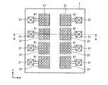
図1は、第1の実施形態による受光装置の構成の一例を模式的に示す平面図である。図2は、第1の実施形態による受光装置の構成の一例を模式的に示す断面図であり、図1のA−A断面図である。受光装置1は、シリコン基板10上に複数の光電変換素子が形成された複数の画素領域21を有する。たとえば、画素領域21は、シリコン基板10の主表面内に2次元的に配置される。シリコン基板10は、たとえば単結晶基板を用いることができる。
第1の実施形態では、光電変換素子の平面視上の形状が矩形状である場合を例に挙げたが、光電変換素子の平面視上の形状は、上記の例の場合に限定されない。第2の実施形態では、光電変換素子の平面視上の形態が他の形状である場合を例に挙げる。
Claims (9)
- 半導体基板の第1主面上に2次元的に設けられる第1導電型の不純物が第1濃度で導入される複数の第1半導体層と、
前記第1半導体層のそれぞれに設けられる光電変換素子と、
隣合う前記光電変換素子の間に設けられる絶縁膜と、
前記第1主面側の前記絶縁膜上に設けられる第1電極と、
前記半導体基板の前記第1主面に対向する第2主面上に設けられる第2電極と、
を備え、
前記光電変換素子は、
前記第1半導体層の前記第1電極が配置される側の上面から所定の深さの範囲に設けられ、第2導電型の不純物が第2濃度で導入される第2半導体層と、
前記第1半導体層内で、前記第1半導体層より浅い範囲の深さで設けられ、前記第2半導体層の側面および下面を囲むように設けられ、前記第1導電型の不純物が前記第1濃度よりも高い第3濃度で導入される第3半導体層と、
を有する受光装置。 - 前記第1半導体層、前記第2半導体層および前記第3半導体層の形状は、平面視上、角部を有さない請求項1に記載の受光装置。
- 前記第1半導体層、前記第2半導体層および前記第3半導体層は、平面視上、丸みを帯びた角部を有する矩形状を有する請求項1に記載の受光装置。
- 前記第1半導体層、前記第2半導体層および前記第3半導体層は、平面視上、円形状を有する請求項1に記載の受光装置。
- 前記第1半導体層、前記第2半導体層および前記第3半導体層は、平面視上、楕円形状を有する請求項1に記載の受光装置。
- 前記第1導電型はP型であり、
前記第2導電型はN型である請求項1から5のいずれか1つに記載の受光装置。 - 前記第1導電型はN型であり、
前記第2導電型はP型である請求項1から5のいずれか1つに記載の受光装置。 - 前記第1半導体層、前記第2半導体層および前記第3半導体層は、エピタキシャル膜によって構成される請求項1に記載の受光装置。
- 半導体基板上に絶縁膜を形成する工程と、
前記絶縁膜に前記半導体基板にまで到達する開口部を形成する工程と、
前記開口部内に、第1導電型の不純物を第1濃度で含む第1半導体層を形成する工程と、
前記第1半導体層の上面から前記半導体基板に到達するまでであってかつ第1深さまでの範囲で、平面視上で前記第1半導体層の形成範囲よりも狭い範囲に、前記第1導電型の不純物を前記第1濃度よりも高い第2濃度で導入して第2半導体層を形成する工程と、
前記第2半導体層の上面から前記第1深さよりも浅い第2深さまでの範囲で、平面視上で前記第2半導体層の形成範囲よりも狭い範囲に、第2導電型の不純物を第3濃度で導入して第3半導体層を形成する工程と、
を含む受光装置の製造方法。
Priority Applications (5)
| Application Number | Priority Date | Filing Date | Title |
|---|---|---|---|
| JP2018046725A JP6878338B2 (ja) | 2018-03-14 | 2018-03-14 | 受光装置および受光装置の製造方法 |
| US16/130,375 US10497823B2 (en) | 2018-03-14 | 2018-09-13 | Light receiving device and method of manufacturing light receiving device |
| EP18200351.7A EP3540788B1 (en) | 2018-03-14 | 2018-10-15 | Light receiving device and method of manufacturing light receiving device |
| KR1020180128944A KR20190108470A (ko) | 2018-03-14 | 2018-10-26 | 수광 장치, 및 수광 장치의 제조 방법 |
| CN201811274379.XA CN110277414A (zh) | 2018-03-14 | 2018-10-30 | 受光装置及受光装置的制造方法 |
Applications Claiming Priority (1)
| Application Number | Priority Date | Filing Date | Title |
|---|---|---|---|
| JP2018046725A JP6878338B2 (ja) | 2018-03-14 | 2018-03-14 | 受光装置および受光装置の製造方法 |
Publications (3)
| Publication Number | Publication Date |
|---|---|
| JP2019161047A JP2019161047A (ja) | 2019-09-19 |
| JP2019161047A5 JP2019161047A5 (ja) | 2020-02-20 |
| JP6878338B2 true JP6878338B2 (ja) | 2021-05-26 |
Family
ID=63857793
Family Applications (1)
| Application Number | Title | Priority Date | Filing Date |
|---|---|---|---|
| JP2018046725A Active JP6878338B2 (ja) | 2018-03-14 | 2018-03-14 | 受光装置および受光装置の製造方法 |
Country Status (5)
| Country | Link |
|---|---|
| US (1) | US10497823B2 (ja) |
| EP (1) | EP3540788B1 (ja) |
| JP (1) | JP6878338B2 (ja) |
| KR (1) | KR20190108470A (ja) |
| CN (1) | CN110277414A (ja) |
Families Citing this family (5)
| Publication number | Priority date | Publication date | Assignee | Title |
|---|---|---|---|---|
| KR20240010101A (ko) | 2017-03-22 | 2024-01-23 | 소니 세미컨덕터 솔루션즈 가부시키가이샤 | 촬상 장치 및 신호 처리 장치 |
| US11393870B2 (en) * | 2018-12-18 | 2022-07-19 | Canon Kabushiki Kaisha | Photoelectric conversion device, imaging system, and mobile apparatus |
| JP7328868B2 (ja) * | 2019-10-30 | 2023-08-17 | 株式会社東芝 | 光検出器、光検出システム、ライダー装置、及び車 |
| JP7325067B2 (ja) * | 2019-10-30 | 2023-08-14 | パナソニックIpマネジメント株式会社 | 光検出器 |
| JP7309647B2 (ja) * | 2020-03-24 | 2023-07-18 | 株式会社東芝 | 受光装置及び半導体装置 |
Family Cites Families (26)
| Publication number | Priority date | Publication date | Assignee | Title |
|---|---|---|---|---|
| JPS6032658B2 (ja) | 1979-07-18 | 1985-07-29 | 住友ノ−ガタック株式会社 | ヒ−トサイクル性に優れる合成樹脂組成物 |
| JPS5911629A (ja) | 1982-07-12 | 1984-01-21 | Toshiba Corp | 表面清浄化方法 |
| JPS5927334A (ja) | 1982-08-06 | 1984-02-13 | Hitachi Ltd | ダイレクトメモリアクセスメモリ装置 |
| US6858829B2 (en) * | 2001-06-20 | 2005-02-22 | Agilent Technologies, Inc. | Avalanche photodiode array biasing device and avalanche photodiode structure |
| JP4841834B2 (ja) * | 2004-12-24 | 2011-12-21 | 浜松ホトニクス株式会社 | ホトダイオードアレイ |
| US7667400B1 (en) * | 2006-06-09 | 2010-02-23 | Array Optronix, Inc. | Back-illuminated Si photomultipliers: structure and fabrication methods |
| CN101484999B (zh) | 2006-07-03 | 2011-09-14 | 浜松光子学株式会社 | 光电二极管阵列 |
| JP5926921B2 (ja) * | 2011-10-21 | 2016-05-25 | 浜松ホトニクス株式会社 | 光検出装置 |
| JP5832852B2 (ja) | 2011-10-21 | 2015-12-16 | 浜松ホトニクス株式会社 | 光検出装置 |
| JP5791461B2 (ja) | 2011-10-21 | 2015-10-07 | 浜松ホトニクス株式会社 | 光検出装置 |
| JP2014241543A (ja) * | 2013-06-12 | 2014-12-25 | 株式会社東芝 | 光検出装置およびct装置 |
| JP6090060B2 (ja) * | 2013-08-23 | 2017-03-08 | 株式会社豊田中央研究所 | シングルフォトンアバランシェダイオード |
| JP2015081863A (ja) | 2013-10-23 | 2015-04-27 | 株式会社東芝 | 光検出器 |
| US9484386B2 (en) | 2013-11-27 | 2016-11-01 | Taiwan Semiconductor Manufacturing Company, Ltd. | Diffraction grating with multiple periodic widths |
| JP2016062996A (ja) * | 2014-09-16 | 2016-04-25 | 株式会社東芝 | 光検出器 |
| JP2016092178A (ja) * | 2014-11-04 | 2016-05-23 | 株式会社リコー | 固体撮像素子 |
| JP6552850B2 (ja) | 2015-03-16 | 2019-07-31 | 株式会社東芝 | 光検出装置 |
| CN114050124A (zh) * | 2015-03-31 | 2022-02-15 | 浜松光子学株式会社 | 半导体装置的制造方法 |
| JP5911629B2 (ja) | 2015-08-04 | 2016-04-27 | 浜松ホトニクス株式会社 | 光検出装置 |
| JP5927334B2 (ja) | 2015-10-28 | 2016-06-01 | 浜松ホトニクス株式会社 | 光検出装置 |
| WO2017169220A1 (ja) * | 2016-03-30 | 2017-10-05 | ソニー株式会社 | 受光装置、撮像装置および電子機器 |
| IT201600079027A1 (it) * | 2016-07-27 | 2018-01-27 | St Microelectronics Srl | Schiera di fotodiodi a valanga operanti in modalita' geiger per la rilevazione di radiazione infrarossa |
| JP6649207B2 (ja) | 2016-08-26 | 2020-02-19 | 株式会社東芝 | 受光装置 |
| JP7058479B2 (ja) * | 2016-10-18 | 2022-04-22 | ソニーセミコンダクタソリューションズ株式会社 | 光検出器 |
| JP6639427B2 (ja) * | 2017-01-13 | 2020-02-05 | 株式会社東芝 | 受光装置 |
| JP6932580B2 (ja) * | 2017-08-04 | 2021-09-08 | ソニーセミコンダクタソリューションズ株式会社 | 固体撮像素子 |
-
2018
- 2018-03-14 JP JP2018046725A patent/JP6878338B2/ja active Active
- 2018-09-13 US US16/130,375 patent/US10497823B2/en not_active Expired - Fee Related
- 2018-10-15 EP EP18200351.7A patent/EP3540788B1/en active Active
- 2018-10-26 KR KR1020180128944A patent/KR20190108470A/ko not_active Application Discontinuation
- 2018-10-30 CN CN201811274379.XA patent/CN110277414A/zh active Pending
Also Published As
| Publication number | Publication date |
|---|---|
| KR20190108470A (ko) | 2019-09-24 |
| CN110277414A (zh) | 2019-09-24 |
| US10497823B2 (en) | 2019-12-03 |
| US20190288149A1 (en) | 2019-09-19 |
| EP3540788B1 (en) | 2021-05-05 |
| EP3540788A1 (en) | 2019-09-18 |
| JP2019161047A (ja) | 2019-09-19 |
Similar Documents
| Publication | Publication Date | Title |
|---|---|---|
| JP6878338B2 (ja) | 受光装置および受光装置の製造方法 | |
| US8871557B2 (en) | Photomultiplier and manufacturing method thereof | |
| EP1840967B1 (en) | Photodiode array | |
| TWI299565B (en) | An image sensing device and fabrication thereof | |
| US8791538B2 (en) | Photodiode array | |
| US8901697B2 (en) | Integrated circuit having a semiconducting via; an integrated circuit including a sensor, such as a photosensitive device, and a method of making said integrated circuit | |
| CN111628034B (zh) | 光电探测装置的制造方法 | |
| JP4703502B2 (ja) | 温度センサおよび赤外線固体撮像装置 | |
| US8664080B2 (en) | Vertical ESD protection device | |
| JP2012174783A (ja) | フォトダイオードおよびフォトダイオードアレイ | |
| KR101768704B1 (ko) | 포토멀티플라이어 및 그의 제조방법 | |
| JP6570750B2 (ja) | 赤外線検出素子および赤外線検出素子の製造方法 | |
| US8569813B2 (en) | Inductive load driving circuit | |
| JP7309647B2 (ja) | 受光装置及び半導体装置 | |
| US20220406823A1 (en) | Image sensor with photosensitivity enhancement region | |
| CN110710000B (zh) | 具有免受环境背光影响的保护的半导体光检测器器件 | |
| US20230042681A1 (en) | Spad pixel for a backside illuminated image sensor | |
| US11049784B2 (en) | Semiconductor device for use in harsh media | |
| US11398572B2 (en) | Semiconductor wafer manufacturing method, method of manufacturing semiconductor energy beam detecting element, and semiconductor wafer | |
| JP4241590B2 (ja) | サージ保護用半導体装置の製造方法 | |
| JP5723135B2 (ja) | 半導体装置の製造方法 | |
| KR20220010947A (ko) | 보호 소자를 갖는 이미지 센싱 장치 | |
| JP2021106196A (ja) | 半導体光検出素子 |
Legal Events
| Date | Code | Title | Description |
|---|---|---|---|
| A521 | Request for written amendment filed |
Free format text: JAPANESE INTERMEDIATE CODE: A523 Effective date: 20200107 |
|
| A621 | Written request for application examination |
Free format text: JAPANESE INTERMEDIATE CODE: A621 Effective date: 20200107 |
|
| A977 | Report on retrieval |
Free format text: JAPANESE INTERMEDIATE CODE: A971007 Effective date: 20201021 |
|
| A131 | Notification of reasons for refusal |
Free format text: JAPANESE INTERMEDIATE CODE: A131 Effective date: 20201208 |
|
| A521 | Request for written amendment filed |
Free format text: JAPANESE INTERMEDIATE CODE: A523 Effective date: 20210205 |
|
| TRDD | Decision of grant or rejection written | ||
| A01 | Written decision to grant a patent or to grant a registration (utility model) |
Free format text: JAPANESE INTERMEDIATE CODE: A01 Effective date: 20210406 |
|
| A61 | First payment of annual fees (during grant procedure) |
Free format text: JAPANESE INTERMEDIATE CODE: A61 Effective date: 20210428 |
|
| R150 | Certificate of patent or registration of utility model |
Ref document number: 6878338 Country of ref document: JP Free format text: JAPANESE INTERMEDIATE CODE: R150 |