JP6878338B2 - Light receiving device and manufacturing method of light receiving device - Google Patents
Light receiving device and manufacturing method of light receiving device Download PDFInfo
- Publication number
- JP6878338B2 JP6878338B2 JP2018046725A JP2018046725A JP6878338B2 JP 6878338 B2 JP6878338 B2 JP 6878338B2 JP 2018046725 A JP2018046725 A JP 2018046725A JP 2018046725 A JP2018046725 A JP 2018046725A JP 6878338 B2 JP6878338 B2 JP 6878338B2
- Authority
- JP
- Japan
- Prior art keywords
- semiconductor layer
- light receiving
- type
- receiving device
- epitaxial layer
- Prior art date
- Legal status (The legal status is an assumption and is not a legal conclusion. Google has not performed a legal analysis and makes no representation as to the accuracy of the status listed.)
- Active
Links
- 238000004519 manufacturing process Methods 0.000 title claims description 8
- 238000006243 chemical reaction Methods 0.000 claims description 47
- 239000004065 semiconductor Substances 0.000 claims description 46
- 239000000758 substrate Substances 0.000 claims description 26
- 239000012535 impurity Substances 0.000 claims description 23
- 238000000034 method Methods 0.000 claims description 13
- 230000015572 biosynthetic process Effects 0.000 claims 2
- XUIMIQQOPSSXEZ-UHFFFAOYSA-N Silicon Chemical compound [Si] XUIMIQQOPSSXEZ-UHFFFAOYSA-N 0.000 description 18
- 229910052710 silicon Inorganic materials 0.000 description 18
- 239000010703 silicon Substances 0.000 description 18
- 230000001681 protective effect Effects 0.000 description 15
- 238000000926 separation method Methods 0.000 description 15
- 238000010791 quenching Methods 0.000 description 13
- 230000000171 quenching effect Effects 0.000 description 13
- 230000000052 comparative effect Effects 0.000 description 9
- 229910052751 metal Inorganic materials 0.000 description 9
- 239000002184 metal Substances 0.000 description 9
- 230000035945 sensitivity Effects 0.000 description 9
- 238000000098 azimuthal photoelectron diffraction Methods 0.000 description 7
- VYPSYNLAJGMNEJ-UHFFFAOYSA-N Silicium dioxide Chemical compound O=[Si]=O VYPSYNLAJGMNEJ-UHFFFAOYSA-N 0.000 description 6
- 238000010586 diagram Methods 0.000 description 6
- 229910052814 silicon oxide Inorganic materials 0.000 description 6
- 238000005229 chemical vapour deposition Methods 0.000 description 3
- 239000012528 membrane Substances 0.000 description 3
- 230000000694 effects Effects 0.000 description 2
- 230000005684 electric field Effects 0.000 description 2
- 239000007789 gas Substances 0.000 description 2
- 238000005468 ion implantation Methods 0.000 description 2
- 238000001020 plasma etching Methods 0.000 description 2
- 229910021420 polycrystalline silicon Inorganic materials 0.000 description 2
- RYGMFSIKBFXOCR-UHFFFAOYSA-N Copper Chemical compound [Cu] RYGMFSIKBFXOCR-UHFFFAOYSA-N 0.000 description 1
- VEXZGXHMUGYJMC-UHFFFAOYSA-N Hydrochloric acid Chemical compound Cl VEXZGXHMUGYJMC-UHFFFAOYSA-N 0.000 description 1
- 229910052782 aluminium Inorganic materials 0.000 description 1
- XAGFODPZIPBFFR-UHFFFAOYSA-N aluminium Chemical compound [Al] XAGFODPZIPBFFR-UHFFFAOYSA-N 0.000 description 1
- 229910052785 arsenic Inorganic materials 0.000 description 1
- 230000002238 attenuated effect Effects 0.000 description 1
- 239000012159 carrier gas Substances 0.000 description 1
- 230000015556 catabolic process Effects 0.000 description 1
- 239000004020 conductor Substances 0.000 description 1
- 229910052802 copper Inorganic materials 0.000 description 1
- 239000010949 copper Substances 0.000 description 1
- 239000013078 crystal Substances 0.000 description 1
- 230000002542 deteriorative effect Effects 0.000 description 1
- ZOCHARZZJNPSEU-UHFFFAOYSA-N diboron Chemical compound B#B ZOCHARZZJNPSEU-UHFFFAOYSA-N 0.000 description 1
- BUMGIEFFCMBQDG-UHFFFAOYSA-N dichlorosilicon Chemical compound Cl[Si]Cl BUMGIEFFCMBQDG-UHFFFAOYSA-N 0.000 description 1
- 238000005530 etching Methods 0.000 description 1
- PCHJSUWPFVWCPO-UHFFFAOYSA-N gold Chemical compound [Au] PCHJSUWPFVWCPO-UHFFFAOYSA-N 0.000 description 1
- 229910052737 gold Inorganic materials 0.000 description 1
- 239000010931 gold Substances 0.000 description 1
- 229910052739 hydrogen Inorganic materials 0.000 description 1
- 239000001257 hydrogen Substances 0.000 description 1
- 125000004435 hydrogen atom Chemical class [H]* 0.000 description 1
- 238000009413 insulation Methods 0.000 description 1
- 238000001459 lithography Methods 0.000 description 1
- 239000000463 material Substances 0.000 description 1
- 239000007769 metal material Substances 0.000 description 1
- 238000012986 modification Methods 0.000 description 1
- 230000004048 modification Effects 0.000 description 1
- 238000000059 patterning Methods 0.000 description 1
- 229920005591 polysilicon Polymers 0.000 description 1
Images


Classifications
-
- H—ELECTRICITY
- H01—ELECTRIC ELEMENTS
- H01L—SEMICONDUCTOR DEVICES NOT COVERED BY CLASS H10
- H01L31/00—Semiconductor devices sensitive to infrared radiation, light, electromagnetic radiation of shorter wavelength or corpuscular radiation and specially adapted either for the conversion of the energy of such radiation into electrical energy or for the control of electrical energy by such radiation; Processes or apparatus specially adapted for the manufacture or treatment thereof or of parts thereof; Details thereof
- H01L31/08—Semiconductor devices sensitive to infrared radiation, light, electromagnetic radiation of shorter wavelength or corpuscular radiation and specially adapted either for the conversion of the energy of such radiation into electrical energy or for the control of electrical energy by such radiation; Processes or apparatus specially adapted for the manufacture or treatment thereof or of parts thereof; Details thereof in which radiation controls flow of current through the device, e.g. photoresistors
- H01L31/10—Semiconductor devices sensitive to infrared radiation, light, electromagnetic radiation of shorter wavelength or corpuscular radiation and specially adapted either for the conversion of the energy of such radiation into electrical energy or for the control of electrical energy by such radiation; Processes or apparatus specially adapted for the manufacture or treatment thereof or of parts thereof; Details thereof in which radiation controls flow of current through the device, e.g. photoresistors characterised by at least one potential-jump barrier or surface barrier, e.g. phototransistors
- H01L31/101—Devices sensitive to infrared, visible or ultraviolet radiation
- H01L31/102—Devices sensitive to infrared, visible or ultraviolet radiation characterised by only one potential barrier or surface barrier
- H01L31/107—Devices sensitive to infrared, visible or ultraviolet radiation characterised by only one potential barrier or surface barrier the potential barrier working in avalanche mode, e.g. avalanche photodiode
-
- H—ELECTRICITY
- H01—ELECTRIC ELEMENTS
- H01L—SEMICONDUCTOR DEVICES NOT COVERED BY CLASS H10
- H01L27/00—Devices consisting of a plurality of semiconductor or other solid-state components formed in or on a common substrate
- H01L27/14—Devices consisting of a plurality of semiconductor or other solid-state components formed in or on a common substrate including semiconductor components sensitive to infrared radiation, light, electromagnetic radiation of shorter wavelength or corpuscular radiation and specially adapted either for the conversion of the energy of such radiation into electrical energy or for the control of electrical energy by such radiation
- H01L27/144—Devices controlled by radiation
- H01L27/1443—Devices controlled by radiation with at least one potential jump or surface barrier
-
- H—ELECTRICITY
- H01—ELECTRIC ELEMENTS
- H01L—SEMICONDUCTOR DEVICES NOT COVERED BY CLASS H10
- H01L27/00—Devices consisting of a plurality of semiconductor or other solid-state components formed in or on a common substrate
- H01L27/14—Devices consisting of a plurality of semiconductor or other solid-state components formed in or on a common substrate including semiconductor components sensitive to infrared radiation, light, electromagnetic radiation of shorter wavelength or corpuscular radiation and specially adapted either for the conversion of the energy of such radiation into electrical energy or for the control of electrical energy by such radiation
- H01L27/144—Devices controlled by radiation
- H01L27/1446—Devices controlled by radiation in a repetitive configuration
-
- H—ELECTRICITY
- H01—ELECTRIC ELEMENTS
- H01L—SEMICONDUCTOR DEVICES NOT COVERED BY CLASS H10
- H01L31/00—Semiconductor devices sensitive to infrared radiation, light, electromagnetic radiation of shorter wavelength or corpuscular radiation and specially adapted either for the conversion of the energy of such radiation into electrical energy or for the control of electrical energy by such radiation; Processes or apparatus specially adapted for the manufacture or treatment thereof or of parts thereof; Details thereof
- H01L31/02—Details
- H01L31/0224—Electrodes
- H01L31/022408—Electrodes for devices characterised by at least one potential jump barrier or surface barrier
- H01L31/022425—Electrodes for devices characterised by at least one potential jump barrier or surface barrier for solar cells
-
- H—ELECTRICITY
- H01—ELECTRIC ELEMENTS
- H01L—SEMICONDUCTOR DEVICES NOT COVERED BY CLASS H10
- H01L31/00—Semiconductor devices sensitive to infrared radiation, light, electromagnetic radiation of shorter wavelength or corpuscular radiation and specially adapted either for the conversion of the energy of such radiation into electrical energy or for the control of electrical energy by such radiation; Processes or apparatus specially adapted for the manufacture or treatment thereof or of parts thereof; Details thereof
- H01L31/0248—Semiconductor devices sensitive to infrared radiation, light, electromagnetic radiation of shorter wavelength or corpuscular radiation and specially adapted either for the conversion of the energy of such radiation into electrical energy or for the control of electrical energy by such radiation; Processes or apparatus specially adapted for the manufacture or treatment thereof or of parts thereof; Details thereof characterised by their semiconductor bodies
- H01L31/0352—Semiconductor devices sensitive to infrared radiation, light, electromagnetic radiation of shorter wavelength or corpuscular radiation and specially adapted either for the conversion of the energy of such radiation into electrical energy or for the control of electrical energy by such radiation; Processes or apparatus specially adapted for the manufacture or treatment thereof or of parts thereof; Details thereof characterised by their semiconductor bodies characterised by their shape or by the shapes, relative sizes or disposition of the semiconductor regions
- H01L31/035272—Semiconductor devices sensitive to infrared radiation, light, electromagnetic radiation of shorter wavelength or corpuscular radiation and specially adapted either for the conversion of the energy of such radiation into electrical energy or for the control of electrical energy by such radiation; Processes or apparatus specially adapted for the manufacture or treatment thereof or of parts thereof; Details thereof characterised by their semiconductor bodies characterised by their shape or by the shapes, relative sizes or disposition of the semiconductor regions characterised by at least one potential jump barrier or surface barrier
- H01L31/035281—Shape of the body
-
- H—ELECTRICITY
- H01—ELECTRIC ELEMENTS
- H01L—SEMICONDUCTOR DEVICES NOT COVERED BY CLASS H10
- H01L31/00—Semiconductor devices sensitive to infrared radiation, light, electromagnetic radiation of shorter wavelength or corpuscular radiation and specially adapted either for the conversion of the energy of such radiation into electrical energy or for the control of electrical energy by such radiation; Processes or apparatus specially adapted for the manufacture or treatment thereof or of parts thereof; Details thereof
- H01L31/0248—Semiconductor devices sensitive to infrared radiation, light, electromagnetic radiation of shorter wavelength or corpuscular radiation and specially adapted either for the conversion of the energy of such radiation into electrical energy or for the control of electrical energy by such radiation; Processes or apparatus specially adapted for the manufacture or treatment thereof or of parts thereof; Details thereof characterised by their semiconductor bodies
- H01L31/036—Semiconductor devices sensitive to infrared radiation, light, electromagnetic radiation of shorter wavelength or corpuscular radiation and specially adapted either for the conversion of the energy of such radiation into electrical energy or for the control of electrical energy by such radiation; Processes or apparatus specially adapted for the manufacture or treatment thereof or of parts thereof; Details thereof characterised by their semiconductor bodies characterised by their crystalline structure or particular orientation of the crystalline planes
-
- H—ELECTRICITY
- H01—ELECTRIC ELEMENTS
- H01L—SEMICONDUCTOR DEVICES NOT COVERED BY CLASS H10
- H01L31/00—Semiconductor devices sensitive to infrared radiation, light, electromagnetic radiation of shorter wavelength or corpuscular radiation and specially adapted either for the conversion of the energy of such radiation into electrical energy or for the control of electrical energy by such radiation; Processes or apparatus specially adapted for the manufacture or treatment thereof or of parts thereof; Details thereof
- H01L31/08—Semiconductor devices sensitive to infrared radiation, light, electromagnetic radiation of shorter wavelength or corpuscular radiation and specially adapted either for the conversion of the energy of such radiation into electrical energy or for the control of electrical energy by such radiation; Processes or apparatus specially adapted for the manufacture or treatment thereof or of parts thereof; Details thereof in which radiation controls flow of current through the device, e.g. photoresistors
- H01L31/10—Semiconductor devices sensitive to infrared radiation, light, electromagnetic radiation of shorter wavelength or corpuscular radiation and specially adapted either for the conversion of the energy of such radiation into electrical energy or for the control of electrical energy by such radiation; Processes or apparatus specially adapted for the manufacture or treatment thereof or of parts thereof; Details thereof in which radiation controls flow of current through the device, e.g. photoresistors characterised by at least one potential-jump barrier or surface barrier, e.g. phototransistors
- H01L31/101—Devices sensitive to infrared, visible or ultraviolet radiation
- H01L31/102—Devices sensitive to infrared, visible or ultraviolet radiation characterised by only one potential barrier or surface barrier
- H01L31/103—Devices sensitive to infrared, visible or ultraviolet radiation characterised by only one potential barrier or surface barrier the potential barrier being of the PN homojunction type
-
- H—ELECTRICITY
- H01—ELECTRIC ELEMENTS
- H01L—SEMICONDUCTOR DEVICES NOT COVERED BY CLASS H10
- H01L31/00—Semiconductor devices sensitive to infrared radiation, light, electromagnetic radiation of shorter wavelength or corpuscular radiation and specially adapted either for the conversion of the energy of such radiation into electrical energy or for the control of electrical energy by such radiation; Processes or apparatus specially adapted for the manufacture or treatment thereof or of parts thereof; Details thereof
- H01L31/18—Processes or apparatus specially adapted for the manufacture or treatment of these devices or of parts thereof
- H01L31/1804—Processes or apparatus specially adapted for the manufacture or treatment of these devices or of parts thereof comprising only elements of Group IV of the Periodic System
-
- Y—GENERAL TAGGING OF NEW TECHNOLOGICAL DEVELOPMENTS; GENERAL TAGGING OF CROSS-SECTIONAL TECHNOLOGIES SPANNING OVER SEVERAL SECTIONS OF THE IPC; TECHNICAL SUBJECTS COVERED BY FORMER USPC CROSS-REFERENCE ART COLLECTIONS [XRACs] AND DIGESTS
- Y02—TECHNOLOGIES OR APPLICATIONS FOR MITIGATION OR ADAPTATION AGAINST CLIMATE CHANGE
- Y02E—REDUCTION OF GREENHOUSE GAS [GHG] EMISSIONS, RELATED TO ENERGY GENERATION, TRANSMISSION OR DISTRIBUTION
- Y02E10/00—Energy generation through renewable energy sources
- Y02E10/50—Photovoltaic [PV] energy
- Y02E10/547—Monocrystalline silicon PV cells
Description
本発明の実施形態は、受光装置および受光装置の製造方法に関する。 An embodiment of the present invention relates to a light receiving device and a method for manufacturing the light receiving device.
従来、クエンチング抵抗およびアバランシェフォトダイオード(以下、APDという)の直列接続を並列に接続し、入射したフォトンの個数を計測する受光装置が開示されている。APDがシリコン(Si)で構成されることからSiPM(Silicon Photomultiplieris)と呼ばれる。このような受光装置で、隣接するAPD間でのクロストークを劣化させないようにしながら、受光感度を上げることが望まれている。 Conventionally, a light receiving device for measuring the number of incident photons by connecting a quenching resistor and an avalanche photodiode (hereinafter referred to as APD) in series in parallel is disclosed. Since APD is composed of silicon (Si), it is called SiPM (Silicon Photomultiplieris). With such a light receiving device, it is desired to increase the light receiving sensitivity while preventing the crosstalk between adjacent APDs from being deteriorated.
本発明の一つの実施形態は、隣接する受光素子間でのクロストークを劣化させずに、受光感度を上げることができる受光素子および受光装置の製造方法を提供することを目的とする。 One object of the present invention is to provide a method for manufacturing a light receiving element and a light receiving device capable of increasing the light receiving sensitivity without deteriorating the crosstalk between adjacent light receiving elements.
本発明の一つの実施形態によれば、半導体基板の第1主面上に2次元的に設けられる第1導電型の不純物が第1濃度で導入される複数の第1半導体層と、第1半導体層のそれぞれに設けられる光電変換素子と、隣合う光電変換素子の間に設けられる絶縁膜と、第1主面側の絶縁膜上に設けられる第1電極と、半導体基板の第1主面に対向する第2主面上に設けられる第2電極と、を備え、光電変換素子は、第1半導体層の第1電極が配置される側の上面から所定の深さの範囲に設けられ、第2導電型の不純物が第2濃度で導入される第2半導体層と、第1半導体層内で、第1半導体層より浅い範囲の深さで設けられ、第2半導体層の側面および下面を囲むように設けられ、第1導電型の不純物が第1濃度よりも高い第3濃度で導入される第3半導体層と、を有する。 According to one embodiment of the present invention, a plurality of first semiconductor layers in which first conductive type impurities provided two-dimensionally on the first main surface of the semiconductor substrate are introduced at a first concentration, and a first semiconductor layer. a photoelectric conversion element provided in each of the semiconductor layers, an insulating film provided between the photoelectric conversion element adjacent a first electrode provided on the first main surface of the insulating film on the first main half-conductor substrate comprising a second electrode provided on the second main surface opposite to the surface, a photoelectric conversion element, arranged from the upper surface of the side where the first electrode of the first semiconductor layer is disposed at a predetermined depth range of The second semiconductor layer, in which the second conductive type impurities are introduced at the second concentration, is provided in the first semiconductor layer at a depth in a range shallower than that of the first semiconductor layer, and the side surface of the second semiconductor layer and provided so as to surround the lower surface, and a third semiconductor layer with impurities of the first conductivity type is introduced at a higher third concentration than the first concentration, the.
以下に添付図面を参照して、実施形態にかかる受光素子および受光装置の製造方法を詳細に説明する。なお、これらの実施形態により本発明が限定されるものではない。また、以下の実施形態で用いられる受光装置の断面図は模式的なものであり、層の厚みと幅との関係や各層の厚みの比率などは現実のものとは異なる場合がある。 The manufacturing method of the light receiving element and the light receiving device according to the embodiment will be described in detail with reference to the accompanying drawings. The present invention is not limited to these embodiments. Further, the cross-sectional view of the light receiving device used in the following embodiments is schematic, and the relationship between the thickness and width of the layers and the ratio of the thickness of each layer may differ from the actual ones.
(第1の実施形態)
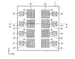
図1は、第1の実施形態による受光装置の構成の一例を模式的に示す平面図である。図2は、第1の実施形態による受光装置の構成の一例を模式的に示す断面図であり、図1のA−A断面図である。受光装置1は、シリコン基板10上に複数の光電変換素子が形成された複数の画素領域21を有する。たとえば、画素領域21は、シリコン基板10の主表面内に2次元的に配置される。シリコン基板10は、たとえば単結晶基板を用いることができる。
(First Embodiment)
FIG. 1 is a plan view schematically showing an example of the configuration of the light receiving device according to the first embodiment. FIG. 2 is a cross-sectional view schematically showing an example of the configuration of the light receiving device according to the first embodiment, and is a cross-sectional view taken along the line AA of FIG. The light receiving device 1 has a plurality of
各画素領域21は、光電変換素子からの出力信号が供給される電極パッド31を有する。画素領域21および電極パッド31は、それぞれ配線41により接続される。電極パッド31は、たとえば外部電極とボンディングワイヤ(図示せず)で接続されるボンディングパッドである。
Each
画素領域21は、シリコン基板10のおもて面(以下、受光面ともいう)上に設けられるSiエピタキシャル層16に形成される。各画素領域21の間には、分離膜13が設けられる。分離膜13として、たとえばシリコン酸化膜が用いられる。各画素領域21のおもて面には、保護膜14が設けられる。保護膜14として、たとえばシリコン酸化膜が用いられる。各画素領域21には、複数の光電変換素子が設けられる。各光電変換素子は、配線61a〜61cを介して、配線41に接続される。
The
シリコン基板10の裏面には金属膜15が形成される。金属膜15は、入射した光を画素領域21側に反射する反射膜としての機能を有する。金属膜15により反射した光が画素領域21に到達することにより、光電変換素子の感度を上げることができる。また、金属膜15は、各光電変換素子の共通電極、ここではアノード電極としての機能を有する。金属膜15として、たとえば、アルミニウム、銅、金などが用いられる。
A
図3は、第1の実施形態による受光装置の画素領域の一部を模式的に示す平面図である。図4は、第1の実施形態による受光装置の断面構造を模式的に示す図であり、図3のB―B断面図である。画素領域21のP型のシリコン基板10上には、P型Siエピタキシャル層161が設けられ、P型Siエピタキシャル層161内に光電変換素子71が設けられる。光電変換素子71は、ガイガーモードで動作するAPDである。ガイガーモードにおいては、各APDのアノードとカソード間にブレークダウン電圧よりも高い逆バイアス電圧が印加される。
FIG. 3 is a plan view schematically showing a part of the pixel region of the light receiving device according to the first embodiment. FIG. 4 is a diagram schematically showing a cross-sectional structure of the light receiving device according to the first embodiment, and is a cross-sectional view taken along the line BB of FIG. A P-type Si
光電変換素子71は、P型Siエピタキシャル層161内に設けられるP+型Siエピタキシャル層162と、P+型Siエピタキシャル層162内に設けられるN+型Siエピタキシャル層163と、を有する。P+型Siエピタキシャル層162およびN+型Siエピタキシャル層163は、光電変換素子71のPN接合を構成する。P+型Siエピタキシャル層162のP型不純物濃度は、P型Siエピタキシャル層161のP型不純物濃度よりも高い。P型Siエピタキシャル層161のP型不純物濃度は、例えば1×10¹⁵/cm3であり、P+型Siエピタキシャル層162のP型不純物濃度は、ピーク濃度で7×1016/cm3であり、N+型Siエピタキシャル層163のN型不純物濃度は、ピーク濃度で1×1019/cm3である。P型Siエピタキシャル層161、P+型Siエピタキシャル層162およびN+型Siエピタキシャル層163は、Siエピタキシャル層16を構成する。
The
光電変換素子71は、図3に示されるように、平面視上で矩形状を有し、シリコン基板10上に2次元的に配置される。図4に示されるように、シリコン基板10上の隣接する光電変換素子71間には、分離膜130が設けられる。分離膜130は、画素領域21間を分離する分離膜13と同じ材料によって構成されてもよく、たとえばシリコン酸化膜からなる。隣接する光電変換素子71間の距離、すなわち分離膜130の幅は、隣接する光電変換素子71で発生した2次光子が減衰して届かない程度の距離とすることができる。光電変換素子71上および分離膜130上には、保護膜14が設けられる。
As shown in FIG. 3, the
図4に示されるように、N+型Siエピタキシャル層163は、上面が保護膜14と接し、他の面がP+型Siエピタキシャル層162と接する。このように、PN接合面積を増やすことで受光感度を上げることができる。
As shown in FIG. 4 , the upper surface of the N + type Si
図3の例では、X方向に延在する保護膜14上の一部には、クエンチング抵抗81が設けられる。クエンチング抵抗81は、光子がAPDに入射し電子雪崩が発生した場合に、その電圧降下によってAPDの増倍作用を終息させる作用を有する。クエンチング抵抗81の抵抗値は、たとえば、数百kΩ程度に設定される。クエンチング抵抗81は、たとえば、多結晶シリコンによって構成される。
In the example of FIG. 3, a
また、Y方向に延在する保護膜14上の一部には、電極膜42が設けられる。電極膜42は、クエンチング抵抗81を介して各光電変換素子71のN+型Siエピタキシャル層163と接続される。具体的には、クエンチング抵抗81の一端から光電変換素子71上の保護膜14に延在する配線91が設けられる。配線91の一方の端部は、クエンチング抵抗81の一端と接続部101を介して接続される。配線91の他方の端部は、光電変換素子71上の保護膜14に設けられる、N+型Siエピタキシャル層163に到達するビアなどの接続部102と接続される。ビアは、たとえば金属材料によって構成される。電極膜42は、各クエンチング抵抗81の他端と接続部103を介して接続される。電極膜42は、光電変換素子71のカソード電極としての機能を有する。なお、上記したように、シリコン基板10の裏面側には、アノード電極としての金属膜15が形成される。
Further, an
図5は、第1の実施形態の受光装置の一部の等価回路を示す図である。各光電変換素子71のアノードは、アノード配線151を介してアノード電極150に接続される。図2および図4に示す金属膜15がアノード配線151として用いられる。なお、アノード配線151は、各画素領域21で共通である。
FIG. 5 is a diagram showing a partial equivalent circuit of the light receiving device of the first embodiment. The anode of each
それぞれの画素領域21内の光電変換素子71のカソードは、クエンチング抵抗81を介してそれぞれの画素領域21毎に設けられる配線41に接続される。配線41は、電極パッド31に電気的に接続される。
The cathode of the
つぎに、このような構成の受光装置1の製造方法について説明する。図6は、第1の実施形態による受光装置の製造方法の一例を模式的に示す断面図である。まず、図6(a)に示されるように、シリコン基板10の主表面に、たとえば、Chemical Vapor Deposition(CVD)法などの成膜法によって絶縁膜131を形成する。絶縁膜131として、シリコン酸化膜などが用いられる。
Next, a method of manufacturing the light receiving device 1 having such a configuration will be described. FIG. 6 is a cross-sectional view schematically showing an example of a method for manufacturing a light receiving device according to the first embodiment. First, as shown in FIG. 6A, an insulating
ついで、絶縁膜131上にレジストを塗布する。その後、図6(b)に示されるように、リソグラフィ技術によって光電変換素子71の形成領域が開口したパターンをレジストに露光し、現像して、レジストパターン141を形成する。
Then, a resist is applied on the insulating
ついで、図6(c)に示されるように、レジストパターン141をマスクとして、Reactive Ion Etching(RIE)法などの異方性エッチングによって、絶縁膜131をエッチングする。これによって、平面視上で矩形状を有する開口300が形成される。上記したように、開口300は、光電変換素子71を形成する領域となる。なお、画素領域21内では、絶縁膜131は、分離膜130となり、画素領域21間では、絶縁膜131は、分離膜13となる。
Then, as shown in FIG. 6C, the insulating
レジストパターン141を除去した後、図6(d)に示されるように、開口300により露出するシリコン基板10の主表面上に、たとえばCVD法によってP型Siエピタキシャル層161を選択的に形成する。キャリアガスとして水素(H2)、ガス種として、たとえばジクロロシラン(SiH2Cl2)、塩化水素(HCl)、P型のドーピングガスとして、ジボラン(B2H6)を用いることができる。P型Siエピタキシャル層161のP型不純物濃度は、例えば1×10¹⁵/cm3である。
After removing the resist
ついで、図6(e)に示されるように、イオン注入法によって、P型Siエピタキシャル層161にさらにP型不純物を導入し、P+型Siエピタキシャル層162を形成する。たとえば、P型不純物濃度がピーク濃度で7×10¹⁶/cm3となるように、BなどのP型不純物をイオン注入する。P+型Siエピタキシャル層162は、P型Siエピタキシャル層161よりも浅い領域に、かつP型Siエピタキシャル層161と同じかP型Siエピタキシャル層161よりも狭い領域に形成される。
Then, as shown in FIG. 6E, a P-type impurity is further introduced into the P-type
さらに、図6(f)に示されるように、イオン注入法によって、P+型Siエピタキシャル層162内にN型不純物を導入し、N+型Siエピタキシャル層163を形成する。たとえば、N型不純物濃度がピーク濃度で1×10¹⁹/cm3となるように、P,AsなどのN型不純物をイオン注入する。また、N+型Siエピタキシャル層163は、P+型Siエピタキシャル層162よりも浅い領域に、かつP+型Siエピタキシャル層162よりも狭い領域に形成される。
Further, as shown in FIG. 6 (f), an N-type impurity is introduced into the P + type Si epitaxial layer 162 by an ion implantation method to form an N + type
その後、シリコン基板10を熱処理することで、P型Siエピタキシャル層161、P+型Siエピタキシャル層162およびN+型Siエピタキシャル層163に導入されたP型不純物およびN型不純物を活性化する。これによって、各開口300にPN接合を有する光電変換素子71が形成される。
Then, the
ついで、光電変換素子71が形成されたシリコン基板10上に、保護膜14を形成する。保護膜14として、たとえばシリコン酸化膜などが用いられる。その後、分離膜130上の所定の位置に、保護膜14を介してクエンチング抵抗81となるポリシリコン膜を形成する。また、N+型Siエピタキシャル層163が形成された領域内の保護膜14に、N+型Siエピタキシャル層163に届くコンタクトホールを形成した後、保護膜14上の全面に導電層を形成する。その後、分離膜130上の所定の位置と、コンタクトホールとクエンチング抵抗81とを結ぶ所定の位置とに、導電膜が残るようにパターニングを行う。これによって、電極膜42と、配線91と、が形成される。そして、シリコン基板10の裏面の全面に、アノード配線となる金属膜15を形成することで、図1〜図3に示される受光装置1が得られる。
Next, the
図7は、比較例による受光装置の画素領域の一部を模式的に示す平面図である。図8は、比較例による受光装置の断面構造を模式的に示す図であり、図7のC―C断面図である。なお、ここでは、光電変換素子よりも上に形成されている保護膜と、カソード配線などの配線層と、を省略している。 FIG. 7 is a plan view schematically showing a part of the pixel region of the light receiving device according to the comparative example. FIG. 8 is a diagram schematically showing a cross-sectional structure of a light receiving device according to a comparative example, and is a cross-sectional view taken along the line CC of FIG. Here, the protective film formed above the photoelectric conversion element and the wiring layer such as the cathode wiring are omitted.
比較例では、P型のシリコン基板10上に、P型Siエピタキシャル層161が配置され、P型Siエピタキシャル層161に光電変換素子71が形成される。光電変換素子71間には、第1の実施形態と同様に、シリコン酸化膜などからなる分離膜130が設けられている。光電変換素子71は、P型Siエピタキシャル層161の上面から所定の深さに設けられるP+型Siエピタキシャル層162と、P+型Siエピタキシャル層162の上面と接し、P+型Siエピタキシャル層162よりも上に設けられるN+型Siエピタキシャル層163と、を有する。P+型Siエピタキシャル層162は、N+型Siエピタキシャル層163よりも基板面内方向のサイズが小さい。また、P+型Siエピタキシャル層162は、N+型Siエピタキシャル層163と上面のみで接している。
In the comparative example, the P-type
受光装置1では、できるだけSN比を高くすることが望まれている。そこで、比較例による受光装置100では、感度を上げるためには、開口率を上げ、受光面積を増やすことが考えられる。受光面積を増やすには、P+型Siエピタキシャル層162の基板面内方向のサイズを増やすことになる。しかし、このようにすると、隣接する光電変換素子71間の距離、すなわち光電変換素子71間に配置される分離膜130の幅が小さくなる。分離膜130の幅が小さくなると、ある光電変換素子71で2次光子が発生すると、隣接する別の光電変換素子71に、2次光子が入射してしまう。つまり、2次光子が発生した光電変換素子71に隣接する別の光電変換素子71では、2次光子を検出するクロストークが劣化し、ノイズが高くなってしまう。その結果、開口率を上げるだけでは、SN比を高くすることができない。このように、比較例の受光装置100では、ノイズを低減することが困難である。
In the light receiving device 1, it is desired to increase the SN ratio as much as possible. Therefore, in the
これに対して、第1の実施形態では、N+型Siエピタキシャル層163の側面および下面を囲むようにP+型Siエピタキシャル層162を配置した光電変換素子71とした。このように、比較例での実効的なPN接合は、面積の小さいP+型Siエピタキシャル層162の上面がN+型Siエピタキシャル層163の下面と接触する部分であるのに対して、第1の実施形態の実効的なPN接合の面積は増加する。その結果、比較例に比して受光感度を上げることができる。また、受光感度を上げることで、隣接する光電変換素子71間の距離を小さくしなくてもよいので、クロストークを劣化させないようにすることもできる。
On the other hand, in the first embodiment, the
なお、N+型Siエピタキシャル層163の側面および下面を囲むようにP+型Siエピタキシャル層162を配置したので、P+型Siエピタキシャル層162の側面および下面を囲むようにN+型Siエピタキシャル層163を配置した場合に比して、受光感度を上げることができる。特に、N+型Siエピタキシャル層163の膜厚を厚くすると、受光面が増加するので、受光感度をより上げることが可能になる。
Since placing the P + -type
(第2の実施形態)
第1の実施形態では、光電変換素子の平面視上の形状が矩形状である場合を例に挙げたが、光電変換素子の平面視上の形状は、上記の例の場合に限定されない。第2の実施形態では、光電変換素子の平面視上の形態が他の形状である場合を例に挙げる。
(Second Embodiment)
In the first embodiment, the case where the photoelectric conversion element has a rectangular shape in a plan view is taken as an example, but the shape of the photoelectric conversion element in a plan view is not limited to the case of the above example. In the second embodiment, a case where the photoelectric conversion element has another shape in a plan view will be taken as an example.
図9は、第2の実施形態による受光装置の画素領域の一部を模式的に示す平面図である。図9(a)では、P型Siエピタキシャル層161、P+型Siエピタキシャル層162およびN+型Siエピタキシャル層163のいずれも、角部が丸みを帯びた矩形状を有している。また、図9(b)では、P型Siエピタキシャル層161、P+型Siエピタキシャル層162およびN+型Siエピタキシャル層163のいずれも円形状を有している。なお、ここに示した形状以外にも、P型Siエピタキシャル層161、P+型Siエピタキシャル層162およびN+型Siエピタキシャル層163が、楕円形上を有していてもよい。なお、その他の構成について、第1の実施形態と同様であるので、その説明を省略する。
FIG. 9 is a plan view schematically showing a part of the pixel region of the light receiving device according to the second embodiment. In FIG. 9A, all of the P-type
第1の実施形態のように、光電変換素子71の平面視上の形状が矩形状を有する場合には、角部において電界集中が生じてしまう。しかし、第2の実施形態では、Siエピタキシャル層16の形状において、角部が生じない形態としたので、電界集中を第1の実施形態に比して抑制することができるという効果を、第1の実施形態の効果に加えて得ることができる。
When the shape of the
なお、上記した説明では、N+型Siエピタキシャル層163の側面および下面を囲むようにP+型Siエピタキシャル層162を配置したが、P+型Siエピタキシャル層162の側面および下面を囲むようにN+型Siエピタキシャル層163を配置してもよい。
In the above description, the P + type
本発明のいくつかの実施形態を説明したが、これらの実施形態は、例として提示したものであり、発明の範囲を限定することは意図していない。これら新規な実施形態は、その他の様々な形態で実施されることが可能であり、発明の要旨を逸脱しない範囲で、種々の省略、置き換え、変更を行うことができる。これら実施形態やその変形は、発明の範囲や要旨に含まれるとともに、特許請求の範囲に記載された発明とその均等の範囲に含まれる。 Although some embodiments of the present invention have been described, these embodiments are presented as examples and are not intended to limit the scope of the invention. These novel embodiments can be implemented in various other embodiments, and various omissions, replacements, and changes can be made without departing from the gist of the invention. These embodiments and modifications thereof are included in the scope and gist of the invention, and are also included in the scope of the invention described in the claims and the equivalent scope thereof.
1 受光装置、10 シリコン基板、13,130 分離膜、14 保護膜、15 金属膜、16 Siエピタキシャル層、21 画素領域、31 電極パッド、41 配線、42 電極膜、61a〜61c 配線、81 クエンチング抵抗、91 配線、101〜103 接続部、131 絶縁膜、141 レジストパターン、150 アノード電極、151 アノード配線、161 P型Siエピタキシャル層、162 P+型Siエピタキシャル層、163 N+型Siエピタキシャル層、300 開口。 1 Light receiving device, 10 Silicon substrate, 13,130 Separation film, 14 Protective film, 15 Metal film, 16 Si epitaxial layer, 21 pixel area, 31 Electrode pad, 41 wiring, 42 electrode film, 61a to 61c wiring, 81 quenching Resistance, 91 wiring, 101-103 connection part, 131 insulation film, 141 resist pattern, 150 anode electrode, 151 anode wiring, 161 P type Si epitaxial layer, 162 P + type Si epitaxial layer, 163 N + type Si epitaxial layer, 300 openings.
Claims (9)
前記第1半導体層のそれぞれに設けられる光電変換素子と、
隣合う前記光電変換素子の間に設けられる絶縁膜と、
前記第1主面側の前記絶縁膜上に設けられる第1電極と、
前記半導体基板の前記第1主面に対向する第2主面上に設けられる第2電極と、
を備え、
前記光電変換素子は、
前記第1半導体層の前記第1電極が配置される側の上面から所定の深さの範囲に設けられ、第2導電型の不純物が第2濃度で導入される第2半導体層と、
前記第1半導体層内で、前記第1半導体層より浅い範囲の深さで設けられ、前記第2半導体層の側面および下面を囲むように設けられ、前記第1導電型の不純物が前記第1濃度よりも高い第3濃度で導入される第3半導体層と、
を有する受光装置。 A plurality of first semiconductor layer a first conductivity type impurity is provided two-dimensionally on the first main surface of the semiconductor substrate is introduced at a first concentration,
A photoelectric conversion element provided in each of the previous SL first semiconductor layer,
An insulating film provided between adjacent photoelectric conversion elements and
The first electrode provided on the insulating film on the first main surface side and
A second electrode provided on the second main surface of the semiconductor substrate facing the first main surface, and
With
The photoelectric conversion element is
A second semiconductor layer provided in a predetermined depth range from the upper surface of the first semiconductor layer on the side where the first electrode is arranged, and a second conductive type impurity is introduced at a second concentration.
In the first semiconductor layer, it is provided at a depth in a range shallower than that of the first semiconductor layer, is provided so as to surround the side surface and the lower surface of the second semiconductor layer, and the first conductive type impurity is the first. A third semiconductor layer introduced at a third concentration higher than the concentration,
A light receiving device having.
前記第2導電型はN型である請求項1から5のいずれか1つに記載の受光装置。 The first conductive type is a P type.
The light receiving device according to any one of claims 1 to 5, wherein the second conductive type is an N type.
前記第2導電型はP型である請求項1から5のいずれか1つに記載の受光装置。 The first conductive type is N type.
The light receiving device according to any one of claims 1 to 5, wherein the second conductive type is a P type.
前記絶縁膜に前記半導体基板にまで到達する開口部を形成する工程と、
前記開口部内に、第1導電型の不純物を第1濃度で含む第1半導体層を形成する工程と、
前記第1半導体層の上面から前記半導体基板に到達するまでであってかつ第1深さまでの範囲で、平面視上で前記第1半導体層の形成範囲よりも狭い範囲に、前記第1導電型の不純物を前記第1濃度よりも高い第2濃度で導入して第2半導体層を形成する工程と、
前記第2半導体層の上面から前記第1深さよりも浅い第2深さまでの範囲で、平面視上で前記第2半導体層の形成範囲よりも狭い範囲に、第2導電型の不純物を第3濃度で導入して第3半導体層を形成する工程と、
を含む受光装置の製造方法。 The process of forming an insulating film on a semiconductor substrate and
A step of forming an opening in the insulating film that reaches the semiconductor substrate, and
A step of forming a first semiconductor layer containing a first conductive type impurity at a first concentration in the opening, and a step of forming the first semiconductor layer.
The first conductive type in a range from the upper surface of the first semiconductor layer to the semiconductor substrate and up to the first depth, in a range narrower than the formation range of the first semiconductor layer in a plan view. To form the second semiconductor layer by introducing the impurities of the above in a second concentration higher than the first concentration.
A third conductive type impurity is placed in a range from the upper surface of the second semiconductor layer to a second depth shallower than the first depth, and in a range narrower than the formation range of the second semiconductor layer in a plan view. The process of introducing at a concentration to form the third semiconductor layer, and
A method for manufacturing a light receiving device including.
Priority Applications (5)
| Application Number | Priority Date | Filing Date | Title |
|---|---|---|---|
| JP2018046725A JP6878338B2 (en) | 2018-03-14 | 2018-03-14 | Light receiving device and manufacturing method of light receiving device |
| US16/130,375 US10497823B2 (en) | 2018-03-14 | 2018-09-13 | Light receiving device and method of manufacturing light receiving device |
| EP18200351.7A EP3540788B1 (en) | 2018-03-14 | 2018-10-15 | Light receiving device and method of manufacturing light receiving device |
| KR1020180128944A KR20190108470A (en) | 2018-03-14 | 2018-10-26 | Light receiving device and manufacturing method of light receiving device |
| CN201811274379.XA CN110277414A (en) | 2018-03-14 | 2018-10-30 | The manufacturing method of light receiving device and light receiving device |
Applications Claiming Priority (1)
| Application Number | Priority Date | Filing Date | Title |
|---|---|---|---|
| JP2018046725A JP6878338B2 (en) | 2018-03-14 | 2018-03-14 | Light receiving device and manufacturing method of light receiving device |
Publications (3)
| Publication Number | Publication Date |
|---|---|
| JP2019161047A JP2019161047A (en) | 2019-09-19 |
| JP2019161047A5 JP2019161047A5 (en) | 2020-02-20 |
| JP6878338B2 true JP6878338B2 (en) | 2021-05-26 |
Family
ID=63857793
Family Applications (1)
| Application Number | Title | Priority Date | Filing Date |
|---|---|---|---|
| JP2018046725A Active JP6878338B2 (en) | 2018-03-14 | 2018-03-14 | Light receiving device and manufacturing method of light receiving device |
Country Status (5)
| Country | Link |
|---|---|
| US (1) | US10497823B2 (en) |
| EP (1) | EP3540788B1 (en) |
| JP (1) | JP6878338B2 (en) |
| KR (1) | KR20190108470A (en) |
| CN (1) | CN110277414A (en) |
Families Citing this family (5)
| Publication number | Priority date | Publication date | Assignee | Title |
|---|---|---|---|---|
| EP3462497A4 (en) * | 2017-03-22 | 2020-04-08 | Sony Semiconductor Solutions Corporation | Imaging device and signal processing device |
| US11393870B2 (en) * | 2018-12-18 | 2022-07-19 | Canon Kabushiki Kaisha | Photoelectric conversion device, imaging system, and mobile apparatus |
| WO2021085484A1 (en) * | 2019-10-30 | 2021-05-06 | パナソニックIpマネジメント株式会社 | Photodetector |
| JP7328868B2 (en) * | 2019-10-30 | 2023-08-17 | 株式会社東芝 | Photodetectors, photodetection systems, lidar devices, and vehicles |
| JP7309647B2 (en) * | 2020-03-24 | 2023-07-18 | 株式会社東芝 | Light receiving device and semiconductor device |
Family Cites Families (26)
| Publication number | Priority date | Publication date | Assignee | Title |
|---|---|---|---|---|
| JPS6032658B2 (en) | 1979-07-18 | 1985-07-29 | 住友ノ−ガタック株式会社 | Synthetic resin composition with excellent heat cycle properties |
| JPS5911629A (en) | 1982-07-12 | 1984-01-21 | Toshiba Corp | Surface cleaning method |
| JPS5927334A (en) | 1982-08-06 | 1984-02-13 | Hitachi Ltd | Direct memory access memory device |
| US6858829B2 (en) * | 2001-06-20 | 2005-02-22 | Agilent Technologies, Inc. | Avalanche photodiode array biasing device and avalanche photodiode structure |
| JP4841834B2 (en) * | 2004-12-24 | 2011-12-21 | 浜松ホトニクス株式会社 | Photodiode array |
| US7667400B1 (en) * | 2006-06-09 | 2010-02-23 | Array Optronix, Inc. | Back-illuminated Si photomultipliers: structure and fabrication methods |
| WO2008004547A1 (en) | 2006-07-03 | 2008-01-10 | Hamamatsu Photonics K.K. | Photodiode array |
| JP5926921B2 (en) * | 2011-10-21 | 2016-05-25 | 浜松ホトニクス株式会社 | Photodetector |
| JP5832852B2 (en) | 2011-10-21 | 2015-12-16 | 浜松ホトニクス株式会社 | Photodetector |
| JP5791461B2 (en) | 2011-10-21 | 2015-10-07 | 浜松ホトニクス株式会社 | Photodetector |
| JP2014241543A (en) * | 2013-06-12 | 2014-12-25 | 株式会社東芝 | Photo-detection device and ct device |
| JP6090060B2 (en) * | 2013-08-23 | 2017-03-08 | 株式会社豊田中央研究所 | Single photon avalanche diode |
| JP2015081863A (en) | 2013-10-23 | 2015-04-27 | 株式会社東芝 | Photodetector |
| US9484386B2 (en) | 2013-11-27 | 2016-11-01 | Taiwan Semiconductor Manufacturing Company, Ltd. | Diffraction grating with multiple periodic widths |
| JP2016062996A (en) * | 2014-09-16 | 2016-04-25 | 株式会社東芝 | Photodetector |
| JP2016092178A (en) * | 2014-11-04 | 2016-05-23 | 株式会社リコー | Solid state imaging device |
| JP6552850B2 (en) | 2015-03-16 | 2019-07-31 | 株式会社東芝 | Light detection device |
| EP3279925B1 (en) * | 2015-03-31 | 2019-12-04 | Hamamatsu Photonics K.K. | Semiconductor device and manufacturing method thereof |
| JP5911629B2 (en) | 2015-08-04 | 2016-04-27 | 浜松ホトニクス株式会社 | Photodetector |
| JP5927334B2 (en) | 2015-10-28 | 2016-06-01 | 浜松ホトニクス株式会社 | Photodetector |
| US20190103501A1 (en) * | 2016-03-30 | 2019-04-04 | Sony Corporation | Light-receiving device, imaging unit, and electronic apparatus |
| IT201600079027A1 (en) * | 2016-07-27 | 2018-01-27 | St Microelectronics Srl | AVALANCHE PHOTOGRAPHING TABLE OPERATING IN GEIGER MODE FOR INFRARED RADIATION DETECTION |
| JP6649207B2 (en) * | 2016-08-26 | 2020-02-19 | 株式会社東芝 | Light receiving device |
| JP7058479B2 (en) * | 2016-10-18 | 2022-04-22 | ソニーセミコンダクタソリューションズ株式会社 | Photodetector |
| JP6639427B2 (en) * | 2017-01-13 | 2020-02-05 | 株式会社東芝 | Light receiving device |
| JP6932580B2 (en) * | 2017-08-04 | 2021-09-08 | ソニーセミコンダクタソリューションズ株式会社 | Solid-state image sensor |
-
2018
- 2018-03-14 JP JP2018046725A patent/JP6878338B2/en active Active
- 2018-09-13 US US16/130,375 patent/US10497823B2/en not_active Expired - Fee Related
- 2018-10-15 EP EP18200351.7A patent/EP3540788B1/en active Active
- 2018-10-26 KR KR1020180128944A patent/KR20190108470A/en not_active Application Discontinuation
- 2018-10-30 CN CN201811274379.XA patent/CN110277414A/en active Pending
Also Published As
| Publication number | Publication date |
|---|---|
| US10497823B2 (en) | 2019-12-03 |
| EP3540788A1 (en) | 2019-09-18 |
| KR20190108470A (en) | 2019-09-24 |
| EP3540788B1 (en) | 2021-05-05 |
| CN110277414A (en) | 2019-09-24 |
| JP2019161047A (en) | 2019-09-19 |
| US20190288149A1 (en) | 2019-09-19 |
Similar Documents
| Publication | Publication Date | Title |
|---|---|---|
| JP6878338B2 (en) | Light receiving device and manufacturing method of light receiving device | |
| US8871557B2 (en) | Photomultiplier and manufacturing method thereof | |
| EP1840967B1 (en) | Photodiode array | |
| TWI299565B (en) | An image sensing device and fabrication thereof | |
| US8791538B2 (en) | Photodiode array | |
| US8901697B2 (en) | Integrated circuit having a semiconducting via; an integrated circuit including a sensor, such as a photosensitive device, and a method of making said integrated circuit | |
| CN111628034B (en) | Method for manufacturing photoelectric detection device | |
| JP4703502B2 (en) | Temperature sensor and infrared solid-state imaging device | |
| US8664080B2 (en) | Vertical ESD protection device | |
| JP2012174783A (en) | Photodiode and photodiode array | |
| KR101768704B1 (en) | photo multiplier and manufacturing method for the same | |
| JP6570750B2 (en) | Infrared detector and method for manufacturing infrared detector | |
| US8569813B2 (en) | Inductive load driving circuit | |
| JP7309647B2 (en) | Light receiving device and semiconductor device | |
| US20220406823A1 (en) | Image sensor with photosensitivity enhancement region | |
| CN110710000B (en) | Semiconductor photodetector device with protection from ambient backlight | |
| US20230042681A1 (en) | Spad pixel for a backside illuminated image sensor | |
| US11049784B2 (en) | Semiconductor device for use in harsh media | |
| US11398572B2 (en) | Semiconductor wafer manufacturing method, method of manufacturing semiconductor energy beam detecting element, and semiconductor wafer | |
| JP4241590B2 (en) | Method of manufacturing a semiconductor device for surge protection | |
| JP5723135B2 (en) | Manufacturing method of semiconductor device | |
| KR20220010947A (en) | Image sensing device having protection device | |
| JP2021106196A (en) | Semiconductor photo detector |
Legal Events
| Date | Code | Title | Description |
|---|---|---|---|
| A521 | Request for written amendment filed |
Free format text: JAPANESE INTERMEDIATE CODE: A523 Effective date: 20200107 |
|
| A621 | Written request for application examination |
Free format text: JAPANESE INTERMEDIATE CODE: A621 Effective date: 20200107 |
|
| A977 | Report on retrieval |
Free format text: JAPANESE INTERMEDIATE CODE: A971007 Effective date: 20201021 |
|
| A131 | Notification of reasons for refusal |
Free format text: JAPANESE INTERMEDIATE CODE: A131 Effective date: 20201208 |
|
| A521 | Request for written amendment filed |
Free format text: JAPANESE INTERMEDIATE CODE: A523 Effective date: 20210205 |
|
| TRDD | Decision of grant or rejection written | ||
| A01 | Written decision to grant a patent or to grant a registration (utility model) |
Free format text: JAPANESE INTERMEDIATE CODE: A01 Effective date: 20210406 |
|
| A61 | First payment of annual fees (during grant procedure) |
Free format text: JAPANESE INTERMEDIATE CODE: A61 Effective date: 20210428 |
|
| R150 | Certificate of patent or registration of utility model |
Ref document number: 6878338 Country of ref document: JP Free format text: JAPANESE INTERMEDIATE CODE: R150 |