JP6737899B2 - プラズマ処理チャンバでのインシトゥチャンバ洗浄効率向上のためのプラズマ処理プロセス - Google Patents
プラズマ処理チャンバでのインシトゥチャンバ洗浄効率向上のためのプラズマ処理プロセス Download PDFInfo
- Publication number
- JP6737899B2 JP6737899B2 JP2018557780A JP2018557780A JP6737899B2 JP 6737899 B2 JP6737899 B2 JP 6737899B2 JP 2018557780 A JP2018557780 A JP 2018557780A JP 2018557780 A JP2018557780 A JP 2018557780A JP 6737899 B2 JP6737899 B2 JP 6737899B2
- Authority
- JP
- Japan
- Prior art keywords
- plasma
- gas
- containing gas
- chamber
- plasma processing
- Prior art date
- Legal status (The legal status is an assumption and is not a legal conclusion. Google has not performed a legal analysis and makes no representation as to the accuracy of the status listed.)
- Expired - Fee Related
Links
- 238000000034 method Methods 0.000 title claims description 127
- 238000012545 processing Methods 0.000 title claims description 115
- 238000004140 cleaning Methods 0.000 title claims description 61
- 238000011065 in-situ storage Methods 0.000 title description 10
- 239000007789 gas Substances 0.000 claims description 165
- 238000009832 plasma treatment Methods 0.000 claims description 47
- 239000000203 mixture Substances 0.000 claims description 40
- 239000000758 substrate Substances 0.000 claims description 38
- 229910052760 oxygen Inorganic materials 0.000 claims description 36
- 235000011194 food seasoning agent Nutrition 0.000 claims description 31
- 239000001257 hydrogen Substances 0.000 claims description 29
- 229910052739 hydrogen Inorganic materials 0.000 claims description 29
- QVGXLLKOCUKJST-UHFFFAOYSA-N atomic oxygen Chemical compound [O] QVGXLLKOCUKJST-UHFFFAOYSA-N 0.000 claims description 27
- 239000001301 oxygen Substances 0.000 claims description 27
- UFHFLCQGNIYNRP-UHFFFAOYSA-N Hydrogen Chemical compound [H][H] UFHFLCQGNIYNRP-UHFFFAOYSA-N 0.000 claims description 25
- 239000000356 contaminant Substances 0.000 claims description 18
- YCKRFDGAMUMZLT-UHFFFAOYSA-N Fluorine atom Chemical compound [F] YCKRFDGAMUMZLT-UHFFFAOYSA-N 0.000 claims description 12
- 239000011737 fluorine Substances 0.000 claims description 12
- 229910052731 fluorine Inorganic materials 0.000 claims description 12
- 229910052751 metal Inorganic materials 0.000 claims description 9
- 239000002184 metal Substances 0.000 claims description 9
- XUIMIQQOPSSXEZ-UHFFFAOYSA-N Silicon Chemical compound [Si] XUIMIQQOPSSXEZ-UHFFFAOYSA-N 0.000 claims description 6
- 229910052710 silicon Inorganic materials 0.000 claims description 6
- 239000010703 silicon Substances 0.000 claims description 6
- 229910002091 carbon monoxide Inorganic materials 0.000 claims description 4
- 229910044991 metal oxide Inorganic materials 0.000 claims description 3
- 150000004706 metal oxides Chemical class 0.000 claims description 3
- 229910018072 Al 2 O 3 Inorganic materials 0.000 claims description 2
- 229910004013 NO 2 Inorganic materials 0.000 claims description 2
- 238000005406 washing Methods 0.000 claims 1
- NJPPVKZQTLUDBO-UHFFFAOYSA-N novaluron Chemical compound C1=C(Cl)C(OC(F)(F)C(OC(F)(F)F)F)=CC=C1NC(=O)NC(=O)C1=C(F)C=CC=C1F NJPPVKZQTLUDBO-UHFFFAOYSA-N 0.000 description 33
- 239000011261 inert gas Substances 0.000 description 15
- 238000009826 distribution Methods 0.000 description 13
- 239000006227 byproduct Substances 0.000 description 12
- 238000000151 deposition Methods 0.000 description 10
- 239000000463 material Substances 0.000 description 10
- 230000008021 deposition Effects 0.000 description 9
- KLZUFWVZNOTSEM-UHFFFAOYSA-K Aluminium flouride Chemical compound F[Al](F)F KLZUFWVZNOTSEM-UHFFFAOYSA-K 0.000 description 7
- 239000012159 carrier gas Substances 0.000 description 7
- 229910052786 argon Inorganic materials 0.000 description 6
- 238000005137 deposition process Methods 0.000 description 6
- 229910052734 helium Inorganic materials 0.000 description 6
- 239000004065 semiconductor Substances 0.000 description 6
- XKRFYHLGVUSROY-UHFFFAOYSA-N Argon Chemical compound [Ar] XKRFYHLGVUSROY-UHFFFAOYSA-N 0.000 description 4
- 238000011109 contamination Methods 0.000 description 4
- 150000002431 hydrogen Chemical class 0.000 description 4
- 239000012686 silicon precursor Substances 0.000 description 4
- IRPGOXJVTQTAAN-UHFFFAOYSA-N 2,2,3,3,3-pentafluoropropanal Chemical compound FC(F)(F)C(F)(F)C=O IRPGOXJVTQTAAN-UHFFFAOYSA-N 0.000 description 3
- 230000002708 enhancing effect Effects 0.000 description 3
- 150000002500 ions Chemical class 0.000 description 3
- 239000000126 substance Substances 0.000 description 3
- 229910016569 AlF 3 Inorganic materials 0.000 description 2
- IJGRMHOSHXDMSA-UHFFFAOYSA-N Atomic nitrogen Chemical compound N#N IJGRMHOSHXDMSA-UHFFFAOYSA-N 0.000 description 2
- VYPSYNLAJGMNEJ-UHFFFAOYSA-N Silicium dioxide Chemical group O=[Si]=O VYPSYNLAJGMNEJ-UHFFFAOYSA-N 0.000 description 2
- BOTDANWDWHJENH-UHFFFAOYSA-N Tetraethyl orthosilicate Chemical compound CCO[Si](OCC)(OCC)OCC BOTDANWDWHJENH-UHFFFAOYSA-N 0.000 description 2
- 229910052782 aluminium Inorganic materials 0.000 description 2
- XAGFODPZIPBFFR-UHFFFAOYSA-N aluminium Chemical compound [Al] XAGFODPZIPBFFR-UHFFFAOYSA-N 0.000 description 2
- 230000003749 cleanliness Effects 0.000 description 2
- 239000011248 coating agent Substances 0.000 description 2
- 238000000576 coating method Methods 0.000 description 2
- PMHQVHHXPFUNSP-UHFFFAOYSA-M copper(1+);methylsulfanylmethane;bromide Chemical compound Br[Cu].CSC PMHQVHHXPFUNSP-UHFFFAOYSA-M 0.000 description 2
- 230000006378 damage Effects 0.000 description 2
- APURLPHDHPNUFL-UHFFFAOYSA-M fluoroaluminum Chemical compound [Al]F APURLPHDHPNUFL-UHFFFAOYSA-M 0.000 description 2
- 239000001307 helium Substances 0.000 description 2
- SWQJXJOGLNCZEY-UHFFFAOYSA-N helium atom Chemical compound [He] SWQJXJOGLNCZEY-UHFFFAOYSA-N 0.000 description 2
- 238000012423 maintenance Methods 0.000 description 2
- 238000004519 manufacturing process Methods 0.000 description 2
- QJGQUHMNIGDVPM-UHFFFAOYSA-N nitrogen group Chemical group [N] QJGQUHMNIGDVPM-UHFFFAOYSA-N 0.000 description 2
- 239000002245 particle Substances 0.000 description 2
- 229910052814 silicon oxide Inorganic materials 0.000 description 2
- 238000003860 storage Methods 0.000 description 2
- JBRZTFJDHDCESZ-UHFFFAOYSA-N AsGa Chemical compound [As]#[Ga] JBRZTFJDHDCESZ-UHFFFAOYSA-N 0.000 description 1
- 229910000599 Cr alloy Inorganic materials 0.000 description 1
- 229910001218 Gallium arsenide Inorganic materials 0.000 description 1
- GPXJNWSHGFTCBW-UHFFFAOYSA-N Indium phosphide Chemical compound [In]#P GPXJNWSHGFTCBW-UHFFFAOYSA-N 0.000 description 1
- 229910018487 Ni—Cr Inorganic materials 0.000 description 1
- CBENFWSGALASAD-UHFFFAOYSA-N Ozone Chemical compound [O-][O+]=O CBENFWSGALASAD-UHFFFAOYSA-N 0.000 description 1
- 229910052581 Si3N4 Inorganic materials 0.000 description 1
- 150000001335 aliphatic alkanes Chemical class 0.000 description 1
- 150000001336 alkenes Chemical class 0.000 description 1
- 238000005513 bias potential Methods 0.000 description 1
- 230000007175 bidirectional communication Effects 0.000 description 1
- 239000000919 ceramic Substances 0.000 description 1
- 229910010293 ceramic material Inorganic materials 0.000 description 1
- 238000006243 chemical reaction Methods 0.000 description 1
- 238000005229 chemical vapour deposition Methods 0.000 description 1
- 239000000788 chromium alloy Substances 0.000 description 1
- BIJOYKCOMBZXAE-UHFFFAOYSA-N chromium iron nickel Chemical compound [Cr].[Fe].[Ni] BIJOYKCOMBZXAE-UHFFFAOYSA-N 0.000 description 1
- VNNRSPGTAMTISX-UHFFFAOYSA-N chromium nickel Chemical compound [Cr].[Ni] VNNRSPGTAMTISX-UHFFFAOYSA-N 0.000 description 1
- 230000001276 controlling effect Effects 0.000 description 1
- 238000010586 diagram Methods 0.000 description 1
- 238000001312 dry etching Methods 0.000 description 1
- 230000009977 dual effect Effects 0.000 description 1
- 239000003344 environmental pollutant Substances 0.000 description 1
- 238000005530 etching Methods 0.000 description 1
- 230000005281 excited state Effects 0.000 description 1
- 239000011521 glass Substances 0.000 description 1
- 230000005484 gravity Effects 0.000 description 1
- 229910001293 incoloy Inorganic materials 0.000 description 1
- TWNQGVIAIRXVLR-UHFFFAOYSA-N oxo(oxoalumanyloxy)alumane Chemical compound O=[Al]O[Al]=O TWNQGVIAIRXVLR-UHFFFAOYSA-N 0.000 description 1
- 230000000737 periodic effect Effects 0.000 description 1
- 229920002120 photoresistant polymer Polymers 0.000 description 1
- 238000005240 physical vapour deposition Methods 0.000 description 1
- 231100000719 pollutant Toxicity 0.000 description 1
- 239000002243 precursor Substances 0.000 description 1
- 230000002028 premature Effects 0.000 description 1
- 239000000047 product Substances 0.000 description 1
- 230000001105 regulatory effect Effects 0.000 description 1
- HQVNEWCFYHHQES-UHFFFAOYSA-N silicon nitride Chemical compound N12[Si]34N5[Si]62N3[Si]51N64 HQVNEWCFYHHQES-UHFFFAOYSA-N 0.000 description 1
- 238000004544 sputter deposition Methods 0.000 description 1
- 230000000087 stabilizing effect Effects 0.000 description 1
- 238000005979 thermal decomposition reaction Methods 0.000 description 1
- 230000003685 thermal hair damage Effects 0.000 description 1
- XLYOFNOQVPJJNP-UHFFFAOYSA-N water Chemical compound O XLYOFNOQVPJJNP-UHFFFAOYSA-N 0.000 description 1
- 238000001039 wet etching Methods 0.000 description 1
Images

Classifications
-
- H—ELECTRICITY
- H01—ELECTRIC ELEMENTS
- H01L—SEMICONDUCTOR DEVICES NOT COVERED BY CLASS H10
- H01L21/00—Processes or apparatus adapted for the manufacture or treatment of semiconductor or solid state devices or of parts thereof
- H01L21/02—Manufacture or treatment of semiconductor devices or of parts thereof
- H01L21/02041—Cleaning
- H01L21/02043—Cleaning before device manufacture, i.e. Begin-Of-Line process
- H01L21/02046—Dry cleaning only
-
- H—ELECTRICITY
- H01—ELECTRIC ELEMENTS
- H01J—ELECTRIC DISCHARGE TUBES OR DISCHARGE LAMPS
- H01J37/00—Discharge tubes with provision for introducing objects or material to be exposed to the discharge, e.g. for the purpose of examination or processing thereof
- H01J37/32—Gas-filled discharge tubes
- H01J37/32009—Arrangements for generation of plasma specially adapted for examination or treatment of objects, e.g. plasma sources
- H01J37/32082—Radio frequency generated discharge
- H01J37/32174—Circuits specially adapted for controlling the RF discharge
-
- H—ELECTRICITY
- H01—ELECTRIC ELEMENTS
- H01J—ELECTRIC DISCHARGE TUBES OR DISCHARGE LAMPS
- H01J37/00—Discharge tubes with provision for introducing objects or material to be exposed to the discharge, e.g. for the purpose of examination or processing thereof
- H01J37/32—Gas-filled discharge tubes
- H01J37/32431—Constructional details of the reactor
- H01J37/32798—Further details of plasma apparatus not provided for in groups H01J37/3244 - H01J37/32788; special provisions for cleaning or maintenance of the apparatus
- H01J37/32853—Hygiene
- H01J37/32862—In situ cleaning of vessels and/or internal parts
-
- H—ELECTRICITY
- H01—ELECTRIC ELEMENTS
- H01L—SEMICONDUCTOR DEVICES NOT COVERED BY CLASS H10
- H01L21/00—Processes or apparatus adapted for the manufacture or treatment of semiconductor or solid state devices or of parts thereof
- H01L21/02—Manufacture or treatment of semiconductor devices or of parts thereof
- H01L21/02104—Forming layers
- H01L21/02107—Forming insulating materials on a substrate
- H01L21/02225—Forming insulating materials on a substrate characterised by the process for the formation of the insulating layer
- H01L21/0226—Forming insulating materials on a substrate characterised by the process for the formation of the insulating layer formation by a deposition process
- H01L21/02263—Forming insulating materials on a substrate characterised by the process for the formation of the insulating layer formation by a deposition process deposition from the gas or vapour phase
- H01L21/02271—Forming insulating materials on a substrate characterised by the process for the formation of the insulating layer formation by a deposition process deposition from the gas or vapour phase deposition by decomposition or reaction of gaseous or vapour phase compounds, i.e. chemical vapour deposition
- H01L21/02274—Forming insulating materials on a substrate characterised by the process for the formation of the insulating layer formation by a deposition process deposition from the gas or vapour phase deposition by decomposition or reaction of gaseous or vapour phase compounds, i.e. chemical vapour deposition in the presence of a plasma [PECVD]
-
- H—ELECTRICITY
- H01—ELECTRIC ELEMENTS
- H01L—SEMICONDUCTOR DEVICES NOT COVERED BY CLASS H10
- H01L21/00—Processes or apparatus adapted for the manufacture or treatment of semiconductor or solid state devices or of parts thereof
- H01L21/02—Manufacture or treatment of semiconductor devices or of parts thereof
- H01L21/04—Manufacture or treatment of semiconductor devices or of parts thereof the devices having at least one potential-jump barrier or surface barrier, e.g. PN junction, depletion layer or carrier concentration layer
- H01L21/18—Manufacture or treatment of semiconductor devices or of parts thereof the devices having at least one potential-jump barrier or surface barrier, e.g. PN junction, depletion layer or carrier concentration layer the devices having semiconductor bodies comprising elements of Group IV of the Periodic System or AIIIBV compounds with or without impurities, e.g. doping materials
- H01L21/30—Treatment of semiconductor bodies using processes or apparatus not provided for in groups H01L21/20 - H01L21/26
- H01L21/302—Treatment of semiconductor bodies using processes or apparatus not provided for in groups H01L21/20 - H01L21/26 to change their surface-physical characteristics or shape, e.g. etching, polishing, cutting
- H01L21/306—Chemical or electrical treatment, e.g. electrolytic etching
- H01L21/3065—Plasma etching; Reactive-ion etching
-
- H—ELECTRICITY
- H01—ELECTRIC ELEMENTS
- H01L—SEMICONDUCTOR DEVICES NOT COVERED BY CLASS H10
- H01L21/00—Processes or apparatus adapted for the manufacture or treatment of semiconductor or solid state devices or of parts thereof
- H01L21/67—Apparatus specially adapted for handling semiconductor or electric solid state devices during manufacture or treatment thereof; Apparatus specially adapted for handling wafers during manufacture or treatment of semiconductor or electric solid state devices or components ; Apparatus not specifically provided for elsewhere
- H01L21/67005—Apparatus not specifically provided for elsewhere
- H01L21/67011—Apparatus for manufacture or treatment
- H01L21/67017—Apparatus for fluid treatment
- H01L21/67028—Apparatus for fluid treatment for cleaning followed by drying, rinsing, stripping, blasting or the like
- H01L21/67034—Apparatus for fluid treatment for cleaning followed by drying, rinsing, stripping, blasting or the like for drying
-
- H—ELECTRICITY
- H01—ELECTRIC ELEMENTS
- H01J—ELECTRIC DISCHARGE TUBES OR DISCHARGE LAMPS
- H01J2237/00—Discharge tubes exposing object to beam, e.g. for analysis treatment, etching, imaging
- H01J2237/32—Processing objects by plasma generation
- H01J2237/33—Processing objects by plasma generation characterised by the type of processing
- H01J2237/334—Etching
-
- H—ELECTRICITY
- H01—ELECTRIC ELEMENTS
- H01J—ELECTRIC DISCHARGE TUBES OR DISCHARGE LAMPS
- H01J2237/00—Discharge tubes exposing object to beam, e.g. for analysis treatment, etching, imaging
- H01J2237/32—Processing objects by plasma generation
- H01J2237/33—Processing objects by plasma generation characterised by the type of processing
- H01J2237/335—Cleaning
Description
Claims (13)
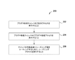
- プラズマ洗浄プロセス後にプラズマ処理プロセスを実行するための方法であって、
基板が内部に配置されていない状態で、プラズマ処理チャンバ内でプラズマ洗浄プロセスを実行することと、
続いて、少なくとも水素含有ガス及び酸素含有ガスを含むプラズマ処理混合ガスを前記プラズマ処理チャンバ内に供給することによって、洗浄後プラズマ処理プロセスを実行することと、ここで前記水素含有ガス及び前記酸素含有ガスは選択的に、別個に前記プラズマ処理チャンバに供給され、
前記プラズマ処理混合ガスからプラズマを形成するために、RFソース電力を前記プラズマ処理チャンバに印加することと、
前記プラズマ処理チャンバの内部表面をプラズマ処理することと、
続いて、前記プラズマ処理チャンバの前記内部表面をプラズマ処理したあとに、シーズニングプロセスを実行することと、を含む方法。 - 前記プラズマ処理混合ガスに供給された前記水素含有ガスが、H2、H2O、NH3又はN2H2を含む、請求項1に記載の方法。
- 前記酸素含有ガスが、O2、H2O、N2O、NO2、O3、CO及びCO2から成る群から選択される、請求項1に記載の方法。
- 前記水素含有ガス及び前記酸素含有ガスが、約1:1から約1:20までの間の流量比で供給される、請求項1に記載の方法。
- 前記水素含有ガスがNH3又はH2であり、前記酸素含有ガスがN2Oである、請求項1に記載の方法。
- 前記シーズニングプロセスを実行することが、
前記プラズマ処理チャンバの前記内部表面にケイ素含有シーズニング膜を形成することを更に含む、請求項1に記載の方法。 - 前記洗浄プロセスを実行することが、
洗浄のために前記プラズマ処理チャンバにフッ素含有ガスを供給することを更に含む、請求項1に記載の方法。 - フッ素含有ガスを供給することが、
前記プラズマ処理チャンバへの供給前に、前記フッ素含有ガスから遠隔プラズマを発生させることを更に含む、請求項7に記載の方法。 - 前記プラズマ処理チャンバの前記内部表面をプラズマ処理することが、
前記プラズマ処理混合ガスから供給された前記水素含有ガスで金属含有汚染物質と反応させることを更に含む、請求項1に記載の方法。 - 前記水素含有ガスで前記金属含有汚染物質と反応させることが、
前記プラズマ処理チャンバの前記プラズマ処理混合ガスからの前記酸素含有ガスによって、前記内部表面に金属酸化物を形成することを更に含む、請求項9に記載の方法。 - 前記金属含有汚染物質がAlFである、請求項9に記載の方法。
- 前記金属酸化物がAl2O3である、請求項10に記載の方法。
- プラズマ洗浄プロセス後にプラズマ処理プロセスを実行するための方法であって、
基板が無い状態でプラズマ処理チャンバに遠隔プラズマ源から供給されたフッ素含有ガスを含む洗浄混合ガスを供給することと、
続いて、プラズマ処理混合ガス内で発生したRFソース電力からプラズマを形成し、前記プラズマ処理チャンバの内部表面から金属汚染物質を除去するために、酸素含有ガス及び水素含有ガスを含むプラズマ処理混合ガスを供給することと、ここで前記水素含有ガス及び前記酸素含有ガスは選択的に、別個に前記プラズマ処理チャンバに供給され、
続いて、前記プラズマ処理チャンバの前記内部表面にシーズニング層を形成するために、シーズニング膜混合ガスを供給することと、を含む方法。
Applications Claiming Priority (3)
| Application Number | Priority Date | Filing Date | Title |
|---|---|---|---|
| US15/145,750 | 2016-05-03 | ||
| US15/145,750 US10002745B2 (en) | 2016-05-03 | 2016-05-03 | Plasma treatment process for in-situ chamber cleaning efficiency enhancement in plasma processing chamber |
| PCT/US2017/027020 WO2017192249A1 (en) | 2016-05-03 | 2017-04-11 | Plasma treatment process for in-situ chamber cleaning efficiency enhancement in plasma processing chamber |
Publications (2)
| Publication Number | Publication Date |
|---|---|
| JP2019515505A JP2019515505A (ja) | 2019-06-06 |
| JP6737899B2 true JP6737899B2 (ja) | 2020-08-12 |
Family
ID=60203108
Family Applications (1)
| Application Number | Title | Priority Date | Filing Date |
|---|---|---|---|
| JP2018557780A Expired - Fee Related JP6737899B2 (ja) | 2016-05-03 | 2017-04-11 | プラズマ処理チャンバでのインシトゥチャンバ洗浄効率向上のためのプラズマ処理プロセス |
Country Status (6)
| Country | Link |
|---|---|
| US (1) | US10002745B2 (ja) |
| JP (1) | JP6737899B2 (ja) |
| KR (1) | KR102158307B1 (ja) |
| CN (1) | CN109075030B (ja) |
| TW (1) | TWI674617B (ja) |
| WO (1) | WO2017192249A1 (ja) |
Families Citing this family (24)
| Publication number | Priority date | Publication date | Assignee | Title |
|---|---|---|---|---|
| WO2018026509A1 (en) * | 2016-08-05 | 2018-02-08 | Applied Materials, Inc. | Aluminum fluoride mitigation by plasma treatment |
| JP6779165B2 (ja) * | 2017-03-29 | 2020-11-04 | 東京エレクトロン株式会社 | 金属汚染防止方法及び成膜装置 |
| US10177017B1 (en) * | 2017-07-05 | 2019-01-08 | Applied Materials, Inc. | Method for conditioning a processing chamber for steady etching rate control |
| CN111919284A (zh) * | 2018-03-01 | 2020-11-10 | 应用材料公司 | 在器件制造中形成金属硬掩模的系统和方法 |
| US20190382889A1 (en) * | 2018-06-15 | 2019-12-19 | Applied Materials, Inc. | Technique to enable high temperature clean for rapid processing of wafers |
| US11355620B2 (en) * | 2018-10-31 | 2022-06-07 | Taiwan Semiconductor Manufacturing Company, Ltd. | FinFET device and method of forming same |
| US20200176232A1 (en) * | 2018-12-04 | 2020-06-04 | Nanya Technology Corporation | Etching device and operating method thereof |
| CN109585276B (zh) * | 2018-12-27 | 2021-06-15 | 上海华力集成电路制造有限公司 | 一种改善多晶硅刻蚀腔体晶圆棍状缺陷的方法 |
| US20210391537A1 (en) * | 2019-01-30 | 2021-12-16 | Applied Materials, Inc. | Method for cleaning a vacuum system, method for vacuum processing of a substrate, and apparatus for vacuum processing a substrate |
| WO2020012693A1 (ja) * | 2019-02-27 | 2020-01-16 | 株式会社 日立ハイテクノロジーズ | プラズマ処理方法及びプラズマ処理装置 |
| TW202119538A (zh) * | 2019-09-19 | 2021-05-16 | 美商應用材料股份有限公司 | 用於清潔基座加熱器的原位dc電漿 |
| WO2021126889A1 (en) * | 2019-12-17 | 2021-06-24 | Applied Materials, Inc. | Surface profiling and texturing of chamber components |
| WO2021161824A1 (ja) * | 2020-02-14 | 2021-08-19 | 東京エレクトロン株式会社 | 基板処理方法および基板処理装置 |
| CN111549325B (zh) * | 2020-06-12 | 2022-10-21 | 北京北方华创微电子装备有限公司 | 一种磁控溅射设备 |
| US11626271B2 (en) * | 2020-06-18 | 2023-04-11 | Tokyo Electron Limited | Surface fluorination remediation for aluminium oxide electrostatic chucks |
| US11674222B2 (en) | 2020-09-29 | 2023-06-13 | Applied Materials, Inc. | Method of in situ ceramic coating deposition |
| TWI779395B (zh) * | 2020-11-16 | 2022-10-01 | 友威科技股份有限公司 | 利用電漿蝕刻去除晶圓缺陷的重工處理設備 |
| CN113481486A (zh) * | 2021-01-20 | 2021-10-08 | 宣城睿晖宣晟企业管理中心合伙企业(有限合伙) | 一种镀膜方法 |
| US11955318B2 (en) | 2021-03-12 | 2024-04-09 | Applied Materials, Inc. | Ash rate recovery method in plasma strip chamber |
| US11837448B2 (en) | 2021-04-27 | 2023-12-05 | Applied Materials, Inc. | High-temperature chamber and chamber component cleaning and maintenance method and apparatus |
| US11699577B2 (en) * | 2021-05-25 | 2023-07-11 | Applied Materials, Inc. | Treatment for high-temperature cleans |
| US11915918B2 (en) * | 2021-06-29 | 2024-02-27 | Applied Materials, Inc. | Cleaning of sin with CCP plasma or RPS clean |
| US11961716B2 (en) * | 2021-12-09 | 2024-04-16 | Industrial Technology Research Institute | Atomic layer deposition method |
| KR20230100595A (ko) | 2021-12-28 | 2023-07-05 | 삼성전기주식회사 | 코일 부품 |
Family Cites Families (19)
| Publication number | Priority date | Publication date | Assignee | Title |
|---|---|---|---|---|
| US5788799A (en) * | 1996-06-11 | 1998-08-04 | Applied Materials, Inc. | Apparatus and method for cleaning of semiconductor process chamber surfaces |
| US6444037B1 (en) * | 1996-11-13 | 2002-09-03 | Applied Materials, Inc. | Chamber liner for high temperature processing chamber |
| WO1998021749A1 (fr) * | 1996-11-14 | 1998-05-22 | Tokyo Electron Limited | Procede de nettoyage d'un dispositif de traitement au plasma et procede de traitement au plasma |
| JP2001335937A (ja) | 2000-05-29 | 2001-12-07 | Mitsubishi Heavy Ind Ltd | 金属汚染低減方法及びプラズマ装置の再生方法 |
| US6868856B2 (en) | 2001-07-13 | 2005-03-22 | Applied Materials, Inc. | Enhanced remote plasma cleaning |
| US20030062064A1 (en) * | 2001-09-28 | 2003-04-03 | Infineon Technologies North America Corp. | Method of removing PECVD residues of fluorinated plasma using in-situ H2 plasma |
| US6872323B1 (en) * | 2001-11-01 | 2005-03-29 | Novellus Systems, Inc. | In situ plasma process to remove fluorine residues from the interior surfaces of a CVD reactor |
| US7097716B2 (en) | 2002-10-17 | 2006-08-29 | Applied Materials, Inc. | Method for performing fluorocarbon chamber cleaning to eliminate fluorine memory effect |
| US7371427B2 (en) * | 2003-05-20 | 2008-05-13 | Applied Materials, Inc. | Reduction of hillocks prior to dielectric barrier deposition in Cu damascene |
| KR100830749B1 (ko) * | 2004-02-19 | 2008-05-20 | 도쿄엘렉트론가부시키가이샤 | 기판 처리 장치에 있어서의 처리실의 클리닝 방법, 기억매체, 플라즈마 처리 장치, 기판 처리 방법 및 클리닝의종점 검출 방법 |
| US20060093756A1 (en) * | 2004-11-03 | 2006-05-04 | Nagarajan Rajagopalan | High-power dielectric seasoning for stable wafer-to-wafer thickness uniformity of dielectric CVD films |
| US7906032B2 (en) * | 2006-03-31 | 2011-03-15 | Tokyo Electron Limited | Method for conditioning a process chamber |
| US7789993B2 (en) * | 2007-02-02 | 2010-09-07 | Applied Materials, Inc. | Internal balanced coil for inductively coupled high density plasma processing chamber |
| US7572647B2 (en) * | 2007-02-02 | 2009-08-11 | Applied Materials, Inc. | Internal balanced coil for inductively coupled high density plasma processing chamber |
| JP5450187B2 (ja) * | 2010-03-16 | 2014-03-26 | 株式会社日立ハイテクノロジーズ | プラズマ処理装置およびプラズマ処理方法 |
| US8999847B2 (en) | 2010-08-16 | 2015-04-07 | Applied Materials, Inc. | a-Si seasoning effect to improve SiN run-to-run uniformity |
| US9533332B2 (en) | 2011-10-06 | 2017-01-03 | Applied Materials, Inc. | Methods for in-situ chamber clean utilized in an etching processing chamber |
| US9269562B2 (en) * | 2013-01-17 | 2016-02-23 | Applied Materials, Inc. | In situ chamber clean with inert hydrogen helium mixture during wafer process |
| JP6476369B2 (ja) * | 2013-03-25 | 2019-03-06 | 株式会社Kokusai Electric | クリーニング方法、半導体装置の製造方法、基板処理装置及びプログラム |
-
2016
- 2016-05-03 US US15/145,750 patent/US10002745B2/en not_active Expired - Fee Related
-
2017
- 2017-04-11 KR KR1020187034567A patent/KR102158307B1/ko active IP Right Grant
- 2017-04-11 JP JP2018557780A patent/JP6737899B2/ja not_active Expired - Fee Related
- 2017-04-11 CN CN201780027736.XA patent/CN109075030B/zh active Active
- 2017-04-11 WO PCT/US2017/027020 patent/WO2017192249A1/en active Application Filing
- 2017-04-25 TW TW106113714A patent/TWI674617B/zh not_active IP Right Cessation
Also Published As
| Publication number | Publication date |
|---|---|
| JP2019515505A (ja) | 2019-06-06 |
| CN109075030A (zh) | 2018-12-21 |
| US20170323768A1 (en) | 2017-11-09 |
| US10002745B2 (en) | 2018-06-19 |
| TWI674617B (zh) | 2019-10-11 |
| KR102158307B1 (ko) | 2020-09-21 |
| KR20180130596A (ko) | 2018-12-07 |
| WO2017192249A1 (en) | 2017-11-09 |
| CN109075030B (zh) | 2023-06-20 |
| TW201804508A (zh) | 2018-02-01 |
Similar Documents
| Publication | Publication Date | Title |
|---|---|---|
| JP6737899B2 (ja) | プラズマ処理チャンバでのインシトゥチャンバ洗浄効率向上のためのプラズマ処理プロセス | |
| JP4514336B2 (ja) | 基板処理装置及びその洗浄方法 | |
| TWI724801B (zh) | 用於具有可重複蝕刻與沉積率之增進效能之調節遠端電漿源的方法 | |
| US6923189B2 (en) | Cleaning of CVD chambers using remote source with cxfyoz based chemistry | |
| KR100447284B1 (ko) | 화학기상증착 챔버의 세정 방법 | |
| TWI254363B (en) | Chamber cleaning method | |
| US20080044593A1 (en) | Method of forming a material layer | |
| JP2006128485A (ja) | 半導体処理装置 | |
| JP2009050854A (ja) | 窒化チタンの除去方法 | |
| JP2016051900A (ja) | 高アスペクト比構造におけるコンタクト洗浄 | |
| KR100786609B1 (ko) | 기구 부품의 반응성 기체 청소 방법 및 공정 | |
| US20210340670A1 (en) | In situ protective coating of chamber components for semiconductor processing | |
| KR102007019B1 (ko) | 플라즈마 처리에 의한 불화 알루미늄 경감 | |
| JP2016086046A (ja) | プラズマ処理方法 | |
| TW202035775A (zh) | 清潔處理腔室的方法 | |
| CN112930580A (zh) | 处理腔室部件的清洁方法 | |
| JP2006319042A (ja) | プラズマクリーニング方法、成膜方法 | |
| JP2020520116A (ja) | 基板及びチャンバ部品上への金属ケイ素化合物層の堆積 | |
| KR20090020925A (ko) | 반도체 장비의 세정방법 | |
| JP2001131752A (ja) | プラズマクリーニング方法 |
Legal Events
| Date | Code | Title | Description |
|---|---|---|---|
| A621 | Written request for application examination |
Free format text: JAPANESE INTERMEDIATE CODE: A621 Effective date: 20190206 |
|
| A977 | Report on retrieval |
Free format text: JAPANESE INTERMEDIATE CODE: A971007 Effective date: 20200122 |
|
| A131 | Notification of reasons for refusal |
Free format text: JAPANESE INTERMEDIATE CODE: A131 Effective date: 20200128 |
|
| A521 | Request for written amendment filed |
Free format text: JAPANESE INTERMEDIATE CODE: A523 Effective date: 20200428 |
|
| TRDD | Decision of grant or rejection written | ||
| A01 | Written decision to grant a patent or to grant a registration (utility model) |
Free format text: JAPANESE INTERMEDIATE CODE: A01 Effective date: 20200623 |
|
| A61 | First payment of annual fees (during grant procedure) |
Free format text: JAPANESE INTERMEDIATE CODE: A61 Effective date: 20200716 |
|
| R150 | Certificate of patent or registration of utility model |
Ref document number: 6737899 Country of ref document: JP Free format text: JAPANESE INTERMEDIATE CODE: R150 |
|
| LAPS | Cancellation because of no payment of annual fees |