JP6737899B2 - Plasma processing process for improving in-situ chamber cleaning efficiency in plasma processing chamber - Google Patents
Plasma processing process for improving in-situ chamber cleaning efficiency in plasma processing chamber Download PDFInfo
- Publication number
- JP6737899B2 JP6737899B2 JP2018557780A JP2018557780A JP6737899B2 JP 6737899 B2 JP6737899 B2 JP 6737899B2 JP 2018557780 A JP2018557780 A JP 2018557780A JP 2018557780 A JP2018557780 A JP 2018557780A JP 6737899 B2 JP6737899 B2 JP 6737899B2
- Authority
- JP
- Japan
- Prior art keywords
- plasma
- gas
- containing gas
- chamber
- plasma processing
- Prior art date
- Legal status (The legal status is an assumption and is not a legal conclusion. Google has not performed a legal analysis and makes no representation as to the accuracy of the status listed.)
- Expired - Fee Related
Links
- 238000000034 method Methods 0.000 title claims description 127
- 238000012545 processing Methods 0.000 title claims description 115
- 238000004140 cleaning Methods 0.000 title claims description 61
- 238000011065 in-situ storage Methods 0.000 title description 10
- 239000007789 gas Substances 0.000 claims description 165
- 238000009832 plasma treatment Methods 0.000 claims description 47
- 239000000203 mixture Substances 0.000 claims description 40
- 239000000758 substrate Substances 0.000 claims description 38
- 229910052760 oxygen Inorganic materials 0.000 claims description 36
- 235000011194 food seasoning agent Nutrition 0.000 claims description 31
- 239000001257 hydrogen Substances 0.000 claims description 29
- 229910052739 hydrogen Inorganic materials 0.000 claims description 29
- QVGXLLKOCUKJST-UHFFFAOYSA-N atomic oxygen Chemical compound [O] QVGXLLKOCUKJST-UHFFFAOYSA-N 0.000 claims description 27
- 239000001301 oxygen Substances 0.000 claims description 27
- UFHFLCQGNIYNRP-UHFFFAOYSA-N Hydrogen Chemical compound [H][H] UFHFLCQGNIYNRP-UHFFFAOYSA-N 0.000 claims description 25
- 239000000356 contaminant Substances 0.000 claims description 18
- YCKRFDGAMUMZLT-UHFFFAOYSA-N Fluorine atom Chemical compound [F] YCKRFDGAMUMZLT-UHFFFAOYSA-N 0.000 claims description 12
- 239000011737 fluorine Substances 0.000 claims description 12
- 229910052731 fluorine Inorganic materials 0.000 claims description 12
- 229910052751 metal Inorganic materials 0.000 claims description 9
- 239000002184 metal Substances 0.000 claims description 9
- XUIMIQQOPSSXEZ-UHFFFAOYSA-N Silicon Chemical compound [Si] XUIMIQQOPSSXEZ-UHFFFAOYSA-N 0.000 claims description 6
- 229910052710 silicon Inorganic materials 0.000 claims description 6
- 239000010703 silicon Substances 0.000 claims description 6
- 229910002091 carbon monoxide Inorganic materials 0.000 claims description 4
- 229910044991 metal oxide Inorganic materials 0.000 claims description 3
- 150000004706 metal oxides Chemical class 0.000 claims description 3
- 229910018072 Al 2 O 3 Inorganic materials 0.000 claims description 2
- 229910004013 NO 2 Inorganic materials 0.000 claims description 2
- 238000005406 washing Methods 0.000 claims 1
- NJPPVKZQTLUDBO-UHFFFAOYSA-N novaluron Chemical compound C1=C(Cl)C(OC(F)(F)C(OC(F)(F)F)F)=CC=C1NC(=O)NC(=O)C1=C(F)C=CC=C1F NJPPVKZQTLUDBO-UHFFFAOYSA-N 0.000 description 33
- 239000011261 inert gas Substances 0.000 description 15
- 238000009826 distribution Methods 0.000 description 13
- 239000006227 byproduct Substances 0.000 description 12
- 238000000151 deposition Methods 0.000 description 10
- 239000000463 material Substances 0.000 description 10
- 230000008021 deposition Effects 0.000 description 9
- KLZUFWVZNOTSEM-UHFFFAOYSA-K Aluminium flouride Chemical compound F[Al](F)F KLZUFWVZNOTSEM-UHFFFAOYSA-K 0.000 description 7
- 239000012159 carrier gas Substances 0.000 description 7
- 229910052786 argon Inorganic materials 0.000 description 6
- 238000005137 deposition process Methods 0.000 description 6
- 229910052734 helium Inorganic materials 0.000 description 6
- 239000004065 semiconductor Substances 0.000 description 6
- XKRFYHLGVUSROY-UHFFFAOYSA-N Argon Chemical compound [Ar] XKRFYHLGVUSROY-UHFFFAOYSA-N 0.000 description 4
- 238000011109 contamination Methods 0.000 description 4
- 150000002431 hydrogen Chemical class 0.000 description 4
- 239000012686 silicon precursor Substances 0.000 description 4
- IRPGOXJVTQTAAN-UHFFFAOYSA-N 2,2,3,3,3-pentafluoropropanal Chemical compound FC(F)(F)C(F)(F)C=O IRPGOXJVTQTAAN-UHFFFAOYSA-N 0.000 description 3
- 230000002708 enhancing effect Effects 0.000 description 3
- 150000002500 ions Chemical class 0.000 description 3
- 239000000126 substance Substances 0.000 description 3
- 229910016569 AlF 3 Inorganic materials 0.000 description 2
- IJGRMHOSHXDMSA-UHFFFAOYSA-N Atomic nitrogen Chemical compound N#N IJGRMHOSHXDMSA-UHFFFAOYSA-N 0.000 description 2
- VYPSYNLAJGMNEJ-UHFFFAOYSA-N Silicium dioxide Chemical group O=[Si]=O VYPSYNLAJGMNEJ-UHFFFAOYSA-N 0.000 description 2
- BOTDANWDWHJENH-UHFFFAOYSA-N Tetraethyl orthosilicate Chemical compound CCO[Si](OCC)(OCC)OCC BOTDANWDWHJENH-UHFFFAOYSA-N 0.000 description 2
- 229910052782 aluminium Inorganic materials 0.000 description 2
- XAGFODPZIPBFFR-UHFFFAOYSA-N aluminium Chemical compound [Al] XAGFODPZIPBFFR-UHFFFAOYSA-N 0.000 description 2
- 230000003749 cleanliness Effects 0.000 description 2
- 239000011248 coating agent Substances 0.000 description 2
- 238000000576 coating method Methods 0.000 description 2
- PMHQVHHXPFUNSP-UHFFFAOYSA-M copper(1+);methylsulfanylmethane;bromide Chemical compound Br[Cu].CSC PMHQVHHXPFUNSP-UHFFFAOYSA-M 0.000 description 2
- 230000006378 damage Effects 0.000 description 2
- APURLPHDHPNUFL-UHFFFAOYSA-M fluoroaluminum Chemical compound [Al]F APURLPHDHPNUFL-UHFFFAOYSA-M 0.000 description 2
- 239000001307 helium Substances 0.000 description 2
- SWQJXJOGLNCZEY-UHFFFAOYSA-N helium atom Chemical compound [He] SWQJXJOGLNCZEY-UHFFFAOYSA-N 0.000 description 2
- 238000012423 maintenance Methods 0.000 description 2
- 238000004519 manufacturing process Methods 0.000 description 2
- QJGQUHMNIGDVPM-UHFFFAOYSA-N nitrogen group Chemical group [N] QJGQUHMNIGDVPM-UHFFFAOYSA-N 0.000 description 2
- 239000002245 particle Substances 0.000 description 2
- 229910052814 silicon oxide Inorganic materials 0.000 description 2
- 238000003860 storage Methods 0.000 description 2
- JBRZTFJDHDCESZ-UHFFFAOYSA-N AsGa Chemical compound [As]#[Ga] JBRZTFJDHDCESZ-UHFFFAOYSA-N 0.000 description 1
- 229910000599 Cr alloy Inorganic materials 0.000 description 1
- 229910001218 Gallium arsenide Inorganic materials 0.000 description 1
- GPXJNWSHGFTCBW-UHFFFAOYSA-N Indium phosphide Chemical compound [In]#P GPXJNWSHGFTCBW-UHFFFAOYSA-N 0.000 description 1
- 229910018487 Ni—Cr Inorganic materials 0.000 description 1
- CBENFWSGALASAD-UHFFFAOYSA-N Ozone Chemical compound [O-][O+]=O CBENFWSGALASAD-UHFFFAOYSA-N 0.000 description 1
- 229910052581 Si3N4 Inorganic materials 0.000 description 1
- 150000001335 aliphatic alkanes Chemical class 0.000 description 1
- 150000001336 alkenes Chemical class 0.000 description 1
- 238000005513 bias potential Methods 0.000 description 1
- 230000007175 bidirectional communication Effects 0.000 description 1
- 239000000919 ceramic Substances 0.000 description 1
- 229910010293 ceramic material Inorganic materials 0.000 description 1
- 238000006243 chemical reaction Methods 0.000 description 1
- 238000005229 chemical vapour deposition Methods 0.000 description 1
- 239000000788 chromium alloy Substances 0.000 description 1
- BIJOYKCOMBZXAE-UHFFFAOYSA-N chromium iron nickel Chemical compound [Cr].[Fe].[Ni] BIJOYKCOMBZXAE-UHFFFAOYSA-N 0.000 description 1
- VNNRSPGTAMTISX-UHFFFAOYSA-N chromium nickel Chemical compound [Cr].[Ni] VNNRSPGTAMTISX-UHFFFAOYSA-N 0.000 description 1
- 230000001276 controlling effect Effects 0.000 description 1
- 238000010586 diagram Methods 0.000 description 1
- 238000001312 dry etching Methods 0.000 description 1
- 230000009977 dual effect Effects 0.000 description 1
- 239000003344 environmental pollutant Substances 0.000 description 1
- 238000005530 etching Methods 0.000 description 1
- 230000005281 excited state Effects 0.000 description 1
- 239000011521 glass Substances 0.000 description 1
- 230000005484 gravity Effects 0.000 description 1
- 229910001293 incoloy Inorganic materials 0.000 description 1
- TWNQGVIAIRXVLR-UHFFFAOYSA-N oxo(oxoalumanyloxy)alumane Chemical compound O=[Al]O[Al]=O TWNQGVIAIRXVLR-UHFFFAOYSA-N 0.000 description 1
- 230000000737 periodic effect Effects 0.000 description 1
- 229920002120 photoresistant polymer Polymers 0.000 description 1
- 238000005240 physical vapour deposition Methods 0.000 description 1
- 231100000719 pollutant Toxicity 0.000 description 1
- 239000002243 precursor Substances 0.000 description 1
- 230000002028 premature Effects 0.000 description 1
- 239000000047 product Substances 0.000 description 1
- 230000001105 regulatory effect Effects 0.000 description 1
- HQVNEWCFYHHQES-UHFFFAOYSA-N silicon nitride Chemical compound N12[Si]34N5[Si]62N3[Si]51N64 HQVNEWCFYHHQES-UHFFFAOYSA-N 0.000 description 1
- 238000004544 sputter deposition Methods 0.000 description 1
- 230000000087 stabilizing effect Effects 0.000 description 1
- 238000005979 thermal decomposition reaction Methods 0.000 description 1
- 230000003685 thermal hair damage Effects 0.000 description 1
- XLYOFNOQVPJJNP-UHFFFAOYSA-N water Chemical compound O XLYOFNOQVPJJNP-UHFFFAOYSA-N 0.000 description 1
- 238000001039 wet etching Methods 0.000 description 1
Images

Classifications
-
- H—ELECTRICITY
- H01—ELECTRIC ELEMENTS
- H01L—SEMICONDUCTOR DEVICES NOT COVERED BY CLASS H10
- H01L21/00—Processes or apparatus adapted for the manufacture or treatment of semiconductor or solid state devices or of parts thereof
- H01L21/02—Manufacture or treatment of semiconductor devices or of parts thereof
- H01L21/02041—Cleaning
- H01L21/02043—Cleaning before device manufacture, i.e. Begin-Of-Line process
- H01L21/02046—Dry cleaning only
-
- H—ELECTRICITY
- H01—ELECTRIC ELEMENTS
- H01J—ELECTRIC DISCHARGE TUBES OR DISCHARGE LAMPS
- H01J37/00—Discharge tubes with provision for introducing objects or material to be exposed to the discharge, e.g. for the purpose of examination or processing thereof
- H01J37/32—Gas-filled discharge tubes
- H01J37/32009—Arrangements for generation of plasma specially adapted for examination or treatment of objects, e.g. plasma sources
- H01J37/32082—Radio frequency generated discharge
- H01J37/32174—Circuits specially adapted for controlling the RF discharge
-
- H—ELECTRICITY
- H01—ELECTRIC ELEMENTS
- H01J—ELECTRIC DISCHARGE TUBES OR DISCHARGE LAMPS
- H01J37/00—Discharge tubes with provision for introducing objects or material to be exposed to the discharge, e.g. for the purpose of examination or processing thereof
- H01J37/32—Gas-filled discharge tubes
- H01J37/32431—Constructional details of the reactor
- H01J37/32798—Further details of plasma apparatus not provided for in groups H01J37/3244 - H01J37/32788; special provisions for cleaning or maintenance of the apparatus
- H01J37/32853—Hygiene
- H01J37/32862—In situ cleaning of vessels and/or internal parts
-
- H—ELECTRICITY
- H01—ELECTRIC ELEMENTS
- H01L—SEMICONDUCTOR DEVICES NOT COVERED BY CLASS H10
- H01L21/00—Processes or apparatus adapted for the manufacture or treatment of semiconductor or solid state devices or of parts thereof
- H01L21/02—Manufacture or treatment of semiconductor devices or of parts thereof
- H01L21/02104—Forming layers
- H01L21/02107—Forming insulating materials on a substrate
- H01L21/02225—Forming insulating materials on a substrate characterised by the process for the formation of the insulating layer
- H01L21/0226—Forming insulating materials on a substrate characterised by the process for the formation of the insulating layer formation by a deposition process
- H01L21/02263—Forming insulating materials on a substrate characterised by the process for the formation of the insulating layer formation by a deposition process deposition from the gas or vapour phase
- H01L21/02271—Forming insulating materials on a substrate characterised by the process for the formation of the insulating layer formation by a deposition process deposition from the gas or vapour phase deposition by decomposition or reaction of gaseous or vapour phase compounds, i.e. chemical vapour deposition
- H01L21/02274—Forming insulating materials on a substrate characterised by the process for the formation of the insulating layer formation by a deposition process deposition from the gas or vapour phase deposition by decomposition or reaction of gaseous or vapour phase compounds, i.e. chemical vapour deposition in the presence of a plasma [PECVD]
-
- H—ELECTRICITY
- H01—ELECTRIC ELEMENTS
- H01L—SEMICONDUCTOR DEVICES NOT COVERED BY CLASS H10
- H01L21/00—Processes or apparatus adapted for the manufacture or treatment of semiconductor or solid state devices or of parts thereof
- H01L21/02—Manufacture or treatment of semiconductor devices or of parts thereof
- H01L21/04—Manufacture or treatment of semiconductor devices or of parts thereof the devices having at least one potential-jump barrier or surface barrier, e.g. PN junction, depletion layer or carrier concentration layer
- H01L21/18—Manufacture or treatment of semiconductor devices or of parts thereof the devices having at least one potential-jump barrier or surface barrier, e.g. PN junction, depletion layer or carrier concentration layer the devices having semiconductor bodies comprising elements of Group IV of the Periodic System or AIIIBV compounds with or without impurities, e.g. doping materials
- H01L21/30—Treatment of semiconductor bodies using processes or apparatus not provided for in groups H01L21/20 - H01L21/26
- H01L21/302—Treatment of semiconductor bodies using processes or apparatus not provided for in groups H01L21/20 - H01L21/26 to change their surface-physical characteristics or shape, e.g. etching, polishing, cutting
- H01L21/306—Chemical or electrical treatment, e.g. electrolytic etching
- H01L21/3065—Plasma etching; Reactive-ion etching
-
- H—ELECTRICITY
- H01—ELECTRIC ELEMENTS
- H01L—SEMICONDUCTOR DEVICES NOT COVERED BY CLASS H10
- H01L21/00—Processes or apparatus adapted for the manufacture or treatment of semiconductor or solid state devices or of parts thereof
- H01L21/67—Apparatus specially adapted for handling semiconductor or electric solid state devices during manufacture or treatment thereof; Apparatus specially adapted for handling wafers during manufacture or treatment of semiconductor or electric solid state devices or components ; Apparatus not specifically provided for elsewhere
- H01L21/67005—Apparatus not specifically provided for elsewhere
- H01L21/67011—Apparatus for manufacture or treatment
- H01L21/67017—Apparatus for fluid treatment
- H01L21/67028—Apparatus for fluid treatment for cleaning followed by drying, rinsing, stripping, blasting or the like
- H01L21/67034—Apparatus for fluid treatment for cleaning followed by drying, rinsing, stripping, blasting or the like for drying
-
- H—ELECTRICITY
- H01—ELECTRIC ELEMENTS
- H01J—ELECTRIC DISCHARGE TUBES OR DISCHARGE LAMPS
- H01J2237/00—Discharge tubes exposing object to beam, e.g. for analysis treatment, etching, imaging
- H01J2237/32—Processing objects by plasma generation
- H01J2237/33—Processing objects by plasma generation characterised by the type of processing
- H01J2237/334—Etching
-
- H—ELECTRICITY
- H01—ELECTRIC ELEMENTS
- H01J—ELECTRIC DISCHARGE TUBES OR DISCHARGE LAMPS
- H01J2237/00—Discharge tubes exposing object to beam, e.g. for analysis treatment, etching, imaging
- H01J2237/32—Processing objects by plasma generation
- H01J2237/33—Processing objects by plasma generation characterised by the type of processing
- H01J2237/335—Cleaning
Description
本開示の実施形態は、概して、プラズマ処理チャンバの洗浄効率をインシトゥ(その場)で向上させるための方法及び装置に関する。特に、本開示の実施形態は、プラズマプロセス後のプラズマ処理チャンバの洗浄効率をインシトゥで高めるために行われるプラズマ処理プロセスのための方法及び装置に関する。 Embodiments of the present disclosure generally relate to methods and apparatus for enhancing cleaning efficiency of plasma processing chambers in-situ. In particular, embodiments of the present disclosure relate to methods and apparatus for plasma processing processes performed to enhance cleaning efficiency of a plasma processing chamber after plasma processing in situ.
半導体処理は、多くの異なる化学的及び物理的プロセスを含み、よって極めて小さな集積回路が基板上で形成される。集積回路を構成する材料の層は、化学気相堆積、物理気相堆積、エピタキシャル成長、化学的処理、電気化学的プロセスなどによって形成される。材料層には、フォトレジストマスク及び湿式又は乾燥エッチング技法を使用してパターン形成されるものもある。集積回路を形成するために利用される基板は、ケイ素、ヒ化ガリウム、リン化インジウム、ガラス、又は他の適切な材料でありうる。 Semiconductor processing involves many different chemical and physical processes, and thus very small integrated circuits are formed on substrates. The layers of material that make up the integrated circuit are formed by chemical vapor deposition, physical vapor deposition, epitaxial growth, chemical treatment, electrochemical processes, and the like. Some material layers are patterned using photoresist masks and wet or dry etching techniques. The substrate utilized to form the integrated circuit can be silicon, gallium arsenide, indium phosphide, glass, or other suitable material.
典型的な半導体処理チャンバは、プロセスゾーンを画定するチャンバ本体と、ガス供給からプロセスゾーンにガスを供給するように適合されたガス分配アセンブリと、プロセスガスを励起して基板支持アセンブリの上に位置付けられた基板を処理するために利用される、プラズマ発生装置といったガス励起器と、ガス排気とを含む。プラズマ処理の間、励起されたガスは、イオン、ラジカル及び処理チャンバ構成要素の露出部分をエッチング及び侵食する高度な反応種、例えば処理中に基板を保持する静電チャックからなることが多い。更に、処理副生成物は、通常、反応性の高いフッ素で定期的に洗浄されなければならないチャンバ構成要素上に堆積されることが多い。したがって、処理チャンバの洗浄性を維持するために、処理チャンバから副生成物を除去するために定期的な洗浄プロセスが実行される。チャンバ構成要素又はチャンバの内壁に堆積した副生成物は、通常、反応性の高い化学物質で定期的に洗浄される。処理及び洗浄中の反応種からの攻撃は、チャンバ構成要素の寿命を短縮し、使用頻度を増加させる。加えて、チャンバ構成要素の侵食された部分からのフッ化アルミニウム(AlF)のようなフレークは、基板処理中の微粒子の汚染源になりうる。更に、洗浄プロセス中に比較的高温の構成要素表面に形成されたAlF3は、洗浄プロセスの後に、昇華するが、後でシャワーヘッドのような比較的低温のチャンバ構成要素表面に堆積する可能性がある。この残留堆積により、早期のチャンバ構成要素の不具合及び頻繁なチャンバのメンテナンスが生じる可能性がある。したがって、処理チャンバの耐用年数を長くし、チャンバの停止時間を短縮し、メンテナンス頻度を低減し、製品歩留まりを改善するために、チャンバ構成要素のプラズマ耐性を促進し、処理及び洗浄中にチャンバ構成要素の損傷を低減することが望ましい。 A typical semiconductor processing chamber includes a chamber body that defines a process zone, a gas distribution assembly that is adapted to supply gas to the process zone from a gas supply, and a process gas that is excited and positioned above the substrate support assembly. A gas exciter, such as a plasma generator, used to process the deposited substrate and a gas exhaust. During plasma processing, the excited gas often consists of ions, radicals and highly reactive species that etch and erode exposed portions of the processing chamber components, such as an electrostatic chuck that holds the substrate during processing. Moreover, process by-products are often deposited on chamber components that typically must be regularly cleaned with highly reactive fluorine. Therefore, in order to maintain the cleanability of the processing chamber, a periodic cleaning process is performed to remove byproducts from the processing chamber. By-products deposited on the chamber components or the inner walls of the chamber are typically periodically cleaned with highly reactive chemicals. Attacks from reactive species during processing and cleaning reduce the life of chamber components and increase their frequency of use. In addition, flakes such as aluminum fluoride (AlF) from the eroded portions of the chamber components can be a source of particulate contamination during substrate processing. In addition, AlF 3 formed on the relatively hot component surfaces during the cleaning process may sublime after the cleaning process but may later be deposited on relatively cold chamber component surfaces such as showerheads. There is. This residual deposition can lead to premature chamber component failure and frequent chamber maintenance. Therefore, in order to prolong the service life of the processing chamber, reduce the down time of the chamber, reduce the maintenance frequency, improve the product yield, promote the plasma resistance of the chamber components, and the chamber configuration during processing and cleaning. It is desirable to reduce element damage.
したがって、処理チャンバの洗浄性を維持するための改善されたプロセス、並びにチャンバ構成要素の寿命を延ばすためにチャンバ構成要素の完全性が必要とされている。 Thus, there is a need for improved processes for maintaining cleanliness of processing chambers, as well as chamber component integrity to extend chamber component life.
本開示の実施形態は、半導体基板製造プロセスに用いられるプラズマ処理チャンバのためのインシトゥチャンバ洗浄効率向上のための方法を含む。1つの実施形態では、プラズマプロセスの洗浄後にプラズマ処理プロセスを実行するための方法は、基板が内部に配置されていない状態で、プラズマ処理チャンバ内で洗浄プロセスを実行することと、続いて、少なくとも水素含有ガス及び/又は酸素含有ガスを含むプラズマ処理混合ガスをプラズマ処理チャンバ内に供給することと、プラズマ処理混合ガスからプラズマを形成するために、RFソース電力を処理チャンバに印加することと、処理チャンバの内部表面をプラズマ処理することとを含む。 Embodiments of the present disclosure include methods for improving in-situ chamber cleaning efficiency for plasma processing chambers used in semiconductor substrate manufacturing processes. In one embodiment, a method for performing a plasma treatment process after cleaning a plasma process includes performing a cleaning process in a plasma treatment chamber without a substrate disposed therein, followed by at least Providing a plasma processing mixture containing a hydrogen-containing gas and/or an oxygen-containing gas into the plasma processing chamber, and applying RF source power to the processing chamber to form a plasma from the plasma processing mixture. Plasma treating the interior surface of the processing chamber.
別の実施形態では、インシトゥチャンバ洗浄のための方法は、基板が内部に配置されていない状態で、プラズマ処理チャンバ内で洗浄プロセスを実行することと、処理チャンバ内でプラズマ処理プロセスをインシトゥで実行することと、処理チャンバ内でのプラズマ処理プロセス後にシーズニングプロセスを実行することとを含み、洗浄プロセス、プラズマ処理プロセス及びシーズニングプロセスは、プラズマ処理チャンバ内で統合された単一の方策によって制御される。 In another embodiment, a method for in-situ chamber cleaning includes performing a cleaning process in a plasma processing chamber with a substrate not disposed therein and in-situ performing the plasma processing process in the processing chamber. Performing and performing a seasoning process after the plasma treatment process in the treatment chamber, the cleaning process, the plasma treatment process and the seasoning process being controlled by a single strategy integrated in the plasma treatment chamber. It
更なる実施形態では、プラズマプロセスの洗浄後にプラズマ処理プロセスを実行するための方法は、プラズマ処理チャンバに遠隔プラズマ源から供給されたフッ素含有ガスを含む洗浄混合ガスを供給することと、プラズマ処理混合ガス内で発生したRFソース電力からプラズマを形成し、前記処理チャンバの内部表面から金属汚染物質を除去するために、酸素含有ガス及び水素含有ガスを含むプラズマ処理混合ガスを供給することと、プラズマ処理チャンバの内部表面にシーズニング層を形成するために、シーズニング膜混合ガスを供給することとを含む。 In a further embodiment, a method for performing a plasma treatment process after cleaning a plasma process includes providing a plasma treatment chamber with a cleaning gas mixture including a fluorine-containing gas supplied from a remote plasma source, and the plasma treatment mixture. Providing a plasma processing mixture gas comprising an oxygen-containing gas and a hydrogen-containing gas to form a plasma from RF source power generated in the gas and remove metal contaminants from the inner surface of the processing chamber; Supplying a seasoning film mixture gas to form a seasoning layer on the inner surface of the processing chamber.
本開示の上述の特徴を詳細に理解できるように、上記で簡単に要約されている本開示のより詳細な説明が、実施形態を参照することによって得られ、それらの実施形態の一部は付随する図面に示されている。しかし、本開示は他の等しく有効な実施形態も許容しうることから、付随する図面は本開示の典型的な実施形態のみを示しており、したがって、本開示の範囲を限定すると見なすべきではないことに、留意されたい。 For a better understanding of the above features of the present disclosure, a more detailed description of the present disclosure, briefly summarized above, may be obtained by reference to the embodiments, some of which are accompanied. Shown in the drawing. However, the accompanying drawings depict only typical embodiments of the present disclosure, as the present disclosure may tolerate other equally effective embodiments, and therefore should not be considered as limiting the scope of the present disclosure. Please note that.
理解を容易にするため、可能な場合には、複数の図に共通する同一の要素を指し示すのに同一の参照番号を使用した。1つの実施形態で開示する要素は、具体的な記述がなくても、他の実施形態で有益に利用できることが企図されている。 For ease of understanding, wherever possible, the same reference numbers have been used to refer to the same elements that are common to multiple figures. It is contemplated that elements disclosed in one embodiment may be beneficially utilized on other embodiments without specific recitation.
本開示の実施形態は、プラズマ処理チャンバ内で実行されるインシトゥ洗浄プロセスの洗浄効率を向上させるための方法及び装置を提供する。1つの例では、洗浄プロセスの洗浄効率は、処理チャンバからプロセス副生成物残留物を除去するためにチャンバ洗浄プロセスの後にプラズマ処理プロセスを実行することによって高められうる。プラズマ処理の間に利用されるプラズマ処理混合ガスの一例は、H2ガスのような水素含有混合ガス、及び/又は酸素含有混合ガスを含む。プラズマ処理プロセスの後に、次いで、処理チャンバの内部表面にシーズニング層をコーティングするために、シーズニングプロセスが実行されてもよい。 Embodiments of the present disclosure provide methods and apparatus for improving the cleaning efficiency of an in-situ cleaning process performed in a plasma processing chamber. In one example, the cleaning efficiency of the cleaning process can be enhanced by performing a plasma processing process after the chamber cleaning process to remove process byproduct residues from the processing chamber. An example of a plasma treatment gas mixture utilized during plasma treatment includes a hydrogen-containing gas mixture, such as H 2 gas, and/or an oxygen-containing gas mixture. After the plasma treatment process, a seasoning process may then be performed to coat the inner surface of the treatment chamber with a seasoning layer.
図1は、半導体デバイス製造のための半導体相互接続構造として利用されうるプラズマプロセスを実行するのに適したプラズマ処理システム132の断面図である。処理システム132は、カリフォルニア州サンタクララの Applied Materials、Inc.から入手可能な適切に適合されたCENTURA(登録商標)、Producer(登録商標)SE又はProducer(登録商標)GT又はProducer(登録商標)XP処理システムでありうる。他の製造業者によって製造されたものを含む他の処理システムは、本明細書に記載された実施形態から恩恵を受けうると考えられる。
FIG. 1 is a cross-sectional view of a
処理システム132は、チャンバ本体151を含む。チャンバ本体151は、内部空間126を画定するリッド125、側壁101及び底壁122を含む。
The
基板支持ペデスタル150が、チャンバ本体151の内部空間126に設けられる。ペデスタル150は、アルミニウム、セラミック、窒化アルミニウム、及び他の適切な材料から製造されうる。1つの実施形態では、ペデスタル150は、ペデスタル150に熱的損傷を引き起こすことなく、プラズマプロセス環境のような高温環境での使用に適した材料である、窒化アルミニウムのようなセラミック材料によって製造される。ペデスタル150は、リフト機構(図示せず)を用いてチャンバ本体151の内部で垂直方向に移動されうる。
The
ペデスタル150は、ペデスタル150上で支持された基板190の温度を制御するのに適した埋め込み式のヒータ要素170を含みうる。1つの実施形態では、ペデスタル150は、電源106からヒータ要素170に電流を印加することによって抵抗加熱されてもよい。1つの実施形態では、ヒータ要素170は、ニッケル−鉄−クロム合金(例えば、INCOLOY(登録商標))シースチューブ内にカプセル化されたニッケル−クロムワイヤから作られてもよい。電源106から供給される電流は、コントローラ110によって調整され、ヒータ要素170によって生成された熱を制御し、それにより、任意の適切な温度範囲での膜堆積中に基板190及びペデスタル150を実質的に一定の温度に維持する。別の実施形態では、ペデスタルは、必要に応じて室温に維持されてもよい。更に別の実施形態では、ペデスタル150はまた、必要に応じて室温よりも低い範囲でペデスタル150を冷却するために、必要に応じてチラー(図示せず)を含みうる。供給される電流は、選択的にペデスタル150の温度を約100℃から約700℃までの間で制御するように調整されうる。
The
熱電対などの温度センサ172は、ペデスタル150の温度を従来の方法でモニタするために、基板支持ペデスタル150に埋め込まれうる。測定された温度は、ヒータ要素170に供給された電力を制御し、基板を所望の温度に維持するために、コントローラ110によって使用される。
A
ペデスタル150は、一般に、それを通して配置されており、従来の方法で、ペデスタル150から基板190を持ち上げ、ロボット(図示せず)で基板190の交換を容易にするように構成されている、複数のリフトピン(図示せず)を含む。
The
ペデスタル150は、ペデスタル150上に基板190を保持するための少なくとも1つの電極192を含む。電極192は、チャック電源108によって駆動され、従来知られているように、基板190をペデスタル表面に保持する静電力を発生させる。代替的には、基板190は、クランプ、真空又は重力によってペデスタル150に保持されてもよい。
The
1つの実施形態では、ペデスタル150は、2つのRFバイアス電源184、186として図1Aに示す、少なくとも1つのRFバイアス電源に結合された電極192が内部に埋め込まれたカソードとして構成される。図1Aに示す例は、2つのRFバイアス電源184、186を示しているが、RFバイアス電源の数は、必要に応じて任意の数でよいことに留意されたい。RFバイアス電源184、186は、ペデスタル150に配置された電極192と、処理システム132のガス分配プレート142又は天井125などの別の電極との間に結合される。RFバイアス電源184、186は、処理システム132の処理領域内に配置されたガスから形成されたプラズマ放電を励起し、維持する。
In one embodiment,
図1に示す実施形態では、デュアルRFバイアス電源184、186は、整合回路104を介してペデスタル150に配置された電極192に結合される。プラズマ処理チャンバ132内に提供された混合ガスをイオン化し、それによって堆積又は他のプラズマ強化処理を実行するために必要なイオンエネルギーを提供するために、RFバイアス電源184、186によって生成された信号が、単一フィードを通じて、整合回路104を通ってペデスタル150に供給される。RFバイアス電源184、186は、一般に、約50kHzから約200MHzの周波数及び約0ワットから約5000ワットの間の電力を有するRF信号を生成することができる。
In the embodiment shown in FIG. 1, dual RF bias
真空ポンプ102は、チャンバ本体151の底部122に形成されたポートに結合される。真空ポンプ102は、チャンバ本体151内に所望のガス圧力を維持するために使用される。真空ポンプ102はまた、後処理ガス及びプロセスの副生成物をチャンバ本体151から排出する。
The
処理システム132は、処理システム132のリッド125を通して結合された一又は複数のガス供給通路144を含む。ガス供給通路144及び真空ポンプ102は、内部空間126内に層流を誘導して粒子汚染を最小にするために、処理システム132の両端に位置付けられる。
The
ガス供給通路144は、遠隔プラズマ源(RPS)148を通してガスパネル193に結合され、混合ガスを内部空間126内に供給する。1つの実施形態では、ガス供給通路144を介して供給される混合ガスは、ガス供給通路144の下方に配置されたガス分配プレート142を通って更に供給されうる。1つの例では、複数の開孔143を有するガス分配プレート142は、ペデスタル150の上方のチャンバ本体151のリッド125に結合される。ガス分配プレート142の開孔143は、プロセスガスをガスパネル193からチャンバ本体151内に導入するために利用される。開孔143は、異なるプロセス要件のための様々なプロセスガスの流れを容易にするために、異なるサイズ、数、分布、形状、設計、及び直径を有しうる。プラズマは、ガス分配プレート142を出るプロセス混合ガスから形成され、プロセスガスの熱分解を高め、基板190の表面191上に材料を堆積させる。
The
ガス分配プレート142及び基板支持ペデスタル150は、内部空間126に一対の離間した電極を形成しうる。一又は複数のRFソース147は、ガス分配プレート142とペデスタル150との間でのプラズマ発生を容易にするために、整合ネットワーク145を介してガス分配プレート142にバイアス電位を供給する。代替的に、RFソース147及び整合ネットワーク145は、ガス分配プレート142、基板支持ペデスタル150に結合されてもよく、又はガス分配プレート142及び基板支持ペデスタル150の両方に結合されてもよく、又はチャンバ本体151の外側に配置されたアンテナ(図示せず)に結合されてもよい。1つの実施形態では、RFソース147は、約30kHzから約13.6MHzの周波数で約10ワットから約3000ワットまでを供給しうる。代替的に、RFソース147は、内部空間126内にプラズマの発生を助けるマイクロ波電力をガス分配プレート142に供給するマイクロ波発振器であってもよい。
The
ガスパネル193から供給されうるガスの例は、ケイ素含有ガス、フッ素連続ガス、酸素含有ガス、水素含有ガス、不活性ガス、及びキャリアガスを含みうる。反応性ガスの適切な例は、SiH4、Si2H6、SiF4、SiH2Cl2、Si4H10、Si5H12、TEOSなどのケイ素含有ガスを含む。適切なキャリアガスは、窒素(N2)、アルゴン(Ar)、水素(H2)、アルカン、アルケン、ヘリウム(He)、酸素(O2)、オゾン(O3)、水蒸気(H2O)などを含む。
Examples of gases that may be supplied from the
1つの実施形態では、遠隔プラズマ源(RPS)148は、代替的には、ガスパネル193から内部空間126内に供給されるガスからプラズマを形成するのを助けるために、ガス供給通路144に結合されうる。遠隔プラズマ源148は、ガスパネル193によって提供される混合ガスから形成されたプラズマを処理システム132に供給する。
In one embodiment, a remote plasma source (RPS) 148 is alternatively coupled to the
コントローラ110は、中央処理装置(CPU)112、メモリ116、及び処理シーケンスを制御し、ガスパネル193からのガス流を調整するために利用される支持回路114を含む。CPU112は、産業用の設定で使用されうる任意の形態の汎用コンピュータプロセッサでありうる。ソフトウェアルーチンは、ランダムアクセスメモリ、読み出し専用メモリ、フロッピー、若しくはハードディスクドライブ、又は他の形態のデジタル記憶ストレージなどのメモリ116に記憶させることができる。サポート回路114は、通常、CPU112に接続され、キャッシュ、クロック回路、入力/出力システム、電源などを含みうる。コントローラ110と処理システム132の様々な構成要素との間の双方向通信は、信号バス118と総称される多数の信号ケーブルを通して処理され、そのいくつかが図1に示される。
The
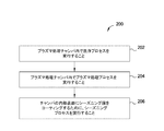
図2は、図1に示すプラズマ処理システム132のようなプラズマ処理チャンバを洗浄した後の洗浄効率を高めるための方法200を示す。方法200は、本開示の実施形態による単一の洗浄ステップ(例えば、単一の洗浄方策)で洗浄効率向上プロセスを統合しうるインシトゥチャンバ洗浄プロセスを含む。
FIG. 2 illustrates a
方法200は、プラズマ処理チャンバ内で洗浄プロセスを実行することにより、動作202で開始する。プラズマ処理システム132が一定期間アイドリングされた後、又はプラズマプロセス(堆積、エッチング、スパッタリング、又は任意のプラズマ関連プロセスを含む)がプラズマ処理システム132において実行された後に、チャンバの残留物若しくは他の汚染物質を除去するために、洗浄プロセスが実行されうる。チャンバ壁、基板ペデスタル、又はプラズマ処理システム132内に配置された他の構成要素を含むプラズマ処理チャンバの内部が、以前のプラズマプロセスから残った状態でその上部に存在する膜の蓄積、副生成物若しくは汚染、又はアイドリング又はラズマ処理中にチャンバの内壁から落ちたフレークを有しうるため、基板が処理システム132から除去された後、または後続の処理のためにプラズマ処理チャンバ内に基板を提供する前に、プラズマ処理チャンバの内部表面を洗浄するために、洗浄プロセスが実行されうる。
洗浄プロセスは、プラズマ処理チャンバの内部から蓄積された汚染物質及び/又は膜を除去し、したがって、後続のプラズマプロセス中に望ましくない粒子が基板ペデスタル上に配置された基板の上に落下することを防止する。動作202で洗浄プロセスを実行している間、例えば、基板が内部に配置されていない際には、基板はプラズマ処理システム132内に存在しない。洗浄プロセスは、プラズマ処理システム132内のチャンバ構成要素又は内壁/構造体を洗浄するために主に実行される。場合によっては、必要に応じて基板ペデスタルの表面を保護するために、その上に配置された膜スタックのないクリーンなケイ素基板などのダミー基板が、処理チャンバ内に配置されうる。
The cleaning process removes accumulated contaminants and/or films from the interior of the plasma processing chamber, thus preventing unwanted particles from falling onto a substrate disposed on the substrate pedestal during a subsequent plasma process. To prevent. During the cleaning process in
1つの例では、プラズマ処理チャンバの内部を洗浄するために、処理システム132に洗浄混合ガスを供給することによって、洗浄プロセスが実行される。洗浄混合ガスは、少なくともフッ素含有ガス及び不活性ガスを含む。1つの実施形態では、洗浄混合ガスに使用されるフッ素含有ガスは、NF3、SF6、HF、CF4などからなる群から選択されうる。不活性ガスは、He又はArなどであってもよい。1つの例では、洗浄混合ガス中に供給されるフッ素含有ガスはNF3ガスであり、不活性ガスはArである。
In one example, the cleaning process is performed by supplying a cleaning gas mixture to the
動作202での洗浄プロセス中に、いくつかのプロセスパラメータが制御されうる。1つの実施形態では、遠隔プラズマ源(図1に示すRPS源148)は、約5000ワットから約20000ワットの間、例えば約10000ワットなどで、プラズマ処理システム132に供給されうる。RPS電力は、RFソース及びバイアス電力の有無にかかわらず処理チャンバに印加されうる。処理チャンバの圧力は、約0.1Torrから約10Torr、例えば約4Torrなど、10Torr未満の圧力範囲で制御されうる。洗浄プロセス中の低圧制御は、洗浄反応の自発性を可能にしうると考えられる。
During the cleaning process at
洗浄混合ガス中に供給されるフッ素含有ガスは、約1sccmから約12000sccmの間、例えば約2800sccmの流量で、処理チャンバに供給されうる。洗浄混合ガス中に供給される不活性ガスは、約1sccmから約300sccmの間、例えば約500sccmの流量で処理チャンバに供給されてうる。 The fluorine-containing gas provided in the cleaning gas mixture may be provided to the processing chamber at a flow rate between about 1 sccm and about 12000 sccm, such as about 2800 sccm. The inert gas provided in the cleaning gas mixture may be provided to the processing chamber at a flow rate between about 1 sccm and about 300 sccm, for example about 500 sccm.
動作202での洗浄プロセスの後、動作204において、プラズマ処理プロセスが次に実行され、処理チャンバ内で行われるプラズマプロセスの別のサイクルの前に、処理システム132に残っている残留物が除去される。上述のように、チャンバ構成要素の過剰洗浄に起因するチャンバフレークのような、洗浄プロセスからの望ましくない残留物が、処理チャンバ内に生成されるか又は残留することがある。処理システム132の洗浄度を高めるために、処理システム132からそのような残留物、特にフッ化アルミニウム(AlF3)、又は他の汚染物質を除去するのを助けるために、動作204でのプラズマ処理プロセスが実行されうる。
After the cleaning process in
実験結果は、プラズマ処理混合ガスからの水素元素及び酸素元素、特に水素元素が、金属含有汚染物質をプラズマ処理チャンバの内部から効率的に除去するために、処理室内に存在するフッ化アルミニウム(AlF3)などの金属含有汚染物質と反応するのを助けることを示した。 The experimental results show that elemental hydrogen and oxygen, especially elemental hydrogen, from the plasma processing mixture gas can effectively remove metal-containing contaminants from the interior of the plasma processing chamber, such as aluminum fluoride (AlF) present in the processing chamber. 3 ) It has been shown to help react with metal-containing contaminants such as.
処理システム132の内部表面をプラズマ処理してフッ化アルミニウム(AlF3)又は他の汚染源と効率的に反応させるために、プラズマ処理混合ガスから形成されたプラズマが使用される。AlF3のような汚染物質は、ラジカル形態のような励起状態に励起され、プラズマ処理混合ガスと容易に反応して、AlH3又はHF*のような揮発性ガス副生成物を形成し、処理システム132から容易にポンピングされる。1つの例では、プラズマ処理混合ガスは、少なくとも1つの水素含有ガス及び/又は酸素含有ガスを含みうる。別の例では、プラズマ処理混合ガスは、複数のサイクルがプラズマ処理プロセスを実行するために、選択的に水素含有ガス及び酸素含有ガスを供給することを含みうる。選択的に水素含有ガスと酸素含有ガスとをプラズマ処理混合ガス中に供給すると、水素含有ガス及び酸素含有ガスは、He又はArのような不活性ガスの有無にかかわらず、別々にかつ個々に供給されうる。
A plasma formed from the plasma treatment gas mixture is used to plasma treat the interior surface of the
水素含有ガスの適切な例は、H2、H2O、NH3、N2H2などである。酸素含有ガスの適切な例は、O2、H2O、O3、H2O2、N2O、NO2、CO、CO2などである。1つの特定の例では、キャリアガス又は不活性ガスはまた、プラズマ処理混合ガス内に供給されてもよい。キャリアガスの適切な例には、窒素(N2)、水素(H2)などが含まれ、不活性ガスの適切な例には、He又はArが含まれる。 Suitable examples of the hydrogen-containing gas, H 2, H 2 O, and the like NH 3, N 2 H 2. Suitable examples of the oxygen-containing gas, and the like O 2, H 2 O, O 3, H 2 O 2, N 2 O, NO 2, CO, CO 2. In one particular example, a carrier gas or an inert gas may also be provided in the plasma processing gas mixture. Suitable examples of carrier gases include nitrogen (N 2 ), hydrogen (H 2 ), etc. Suitable examples of inert gases include He or Ar.
1つの特定の例では、プラズマ処理混合ガスに使用される水素含有ガスは、H2又はNH3である。プラズマ処理混合ガスで使用される酸素含有ガスは、N2O又はO2である。プラズマ混合ガスに使用されるキャリアガスはN2であり、プラズマ処理混合ガスに使用される不活性ガスはArである。 In one particular example, the hydrogen-containing gas used in the plasma treatment gas mixture is H 2 or NH 3 . The oxygen-containing gas used in the plasma treatment mixed gas is N 2 O or O 2 . The carrier gas used for the plasma mixed gas is N 2 and the inert gas used for the plasma treated mixed gas is Ar.
プラズマ処理プロセス中にプラズマ処理混合ガスに含まれる水素含有ガスは、大量の水素元素を供給し、水素元素は、フッ化アルミニウムのような金属含有汚染物質中のフッ素元素と反応して、AlH3又はHFなどの揮発性ガス副生成物を形成し、処理システム132から容易にポンピングされると考えられる。その後、AlH3のような揮発性ガス副生成物は、処理チャンバ内でAl*又はH2ガスとして更に分解されうる。更に、酸素含有ガスからの酸素元素は、次いでアルミニウム活性種(Al*又はAl−など)などの活性金属汚染物質と反応することがあり、酸化アルミニウム(Al2O3)などの金属酸化物を形成し、したがって、チャンバ構成要素の表面上の薄層を安定化処理し、チャンバ構成要素の表面が更に損傷又は攻撃するのを防止する。従って、少なくとも水素含有ガスと酸素含有ガスとを含むプラズマ処理混合ガスを利用することによって、処理チャンバの内面が効率的に洗浄されうる。
The hydrogen-containing gas contained in the plasma treatment mixture during the plasma treatment process supplies a large amount of elemental hydrogen, which reacts with elemental fluorine in metal-containing contaminants such as aluminum fluoride to produce AlH 3 Alternatively, it may form volatile gas byproducts such as HF and be easily pumped from the
いくつかの実施形態では、不活性ガス(Ar又はHeなど)又はキャリアガス(N2又はN2Oなど)が、プラズマ処理混合ガス中に供給されうる。プラズマ処理混合ガス中に供給される不活性ガスは、プラズマ処理混合ガスから形成されたプラズマ中のイオンの寿命を延ばすのを助けうると考えられる。イオンの寿命の増加は、フッ化アルミニウム(AlF3)又は他の汚染物質源をより完全に反応及び活性化させるのを助けることがあり、フッ化アルミニウム(AlF3)又は処理システム132からの他の汚染物質源の除去が高められる。
In some embodiments, an inert gas (such as Ar or He) or a carrier gas (such as N 2 or N 2 O) can be provided in the plasma treatment gas mixture. It is believed that the inert gas provided in the plasma-treated mixed gas can help extend the life of the ions in the plasma formed from the plasma-treated mixed gas. Increasing ionic lifespan, it may help to aluminum fluoride (AlF 3) or another source of contaminants more completely reacted and activated, other from aluminum fluoride (AlF 3) or
動作204におけるプラズマ処理プロセス中に、いくつかのプロセスパラメータが制御されうる。1つの実施形態では、RFソース147によって供給される電力などのRFソース電力は、約50ワットから約2500ワット、例えば約750ワットなどが供給されうる。RFソース電力は、RPS電力又はRFソースバイアス電力の有無にかかわらず、処理チャンバに印加されうる。処理チャンバの圧力は、約0.1Torrから約10Torrまでの間、例えば約4.5Torrのなど、10Torr未満の圧力範囲で制御されうる。
Several process parameters may be controlled during the plasma treatment process in
プラズマ処理混合ガス中に供給される水素含有ガスは、約1sccmから約5000sccmまでの間、例えば約700sccmの流量で、処理チャンバ内に供給されうる。プラズマ処理混合ガス物中に供給される不活性ガス、例えばArガスは、約100sccmから約8000sccmまでの間、例えば約3600sccmの流量で、処理チャンバに供給されうる。プラズマ処理混合ガス中に供給されるN2ガスなどのキャリアガスは、約100sccmから約5000sccmまでの間、例えば約1500sccmの流量で、処理チャンバに供給されうる。プラズマ処理混合ガス中に供給されるN2Oのような酸素含有ガスは、約50sccmから約50000sccmまでの間、例えば約11000sccmの流量で、処理チャンバに供給されうる。一又は複数の実施形態では、水素含有ガス対酸素含有ガスの少なくとも1:30の流量比、例えば、約1:1から1:20までの間、例えば約1:15の比などを有するプラズマ処理混合ガスを供給するために、ガスが加えられる。 The hydrogen-containing gas provided in the plasma processing mixture may be provided in the processing chamber at a flow rate between about 1 sccm and about 5000 sccm, for example about 700 sccm. The inert gas, such as Ar gas, provided in the plasma treatment mixture may be provided to the treatment chamber at a flow rate between about 100 seem and about 8000 seem, for example about 3600 seem. A carrier gas, such as N 2 gas, supplied in the plasma processing mixture may be supplied to the processing chamber at a flow rate between about 100 sccm and about 5000 sccm, for example about 1500 sccm. An oxygen-containing gas, such as N 2 O, supplied in the plasma processing gas mixture may be supplied to the processing chamber at a flow rate between about 50 sccm and about 50,000 sccm, for example about 11000 sccm. In one or more embodiments, plasma treatment having a flow ratio of hydrogen-containing gas to oxygen-containing gas of at least 1:30, such as between about 1:1 and 1:20, such as about 1:15. Gas is added to provide the mixed gas.
処理チャンバに導入される各ガスの量は、例えば、除去されるチャンバ残留物の厚さ又は量、洗浄される基板の形状寸法、プラズマの空間容量、チャンバ本体の空間容量、及びチャンバ本体に結合された真空システムの能力に適応するように、変更及び調整されうる。 The amount of each gas introduced into the processing chamber depends on, for example, the thickness or amount of chamber residue to be removed, the geometry of the substrate to be cleaned, the spatial volume of the plasma, the spatial volume of the chamber body, and the chamber body. Can be modified and adjusted to accommodate the capabilities of the vacuum system in place.
動作206では、動作204のプラズマ処理プロセスの後、シーズニングプロセスが実行されうる。上述のように、一又は複数の基板が処理システム132で処理された後、典型的には、チャンバ壁に堆積され蓄積された堆積副生成物を除去するために、動作202における洗浄プロセスが実行される。チャンバ壁が洗浄ガスによって十分に洗浄された後、動作204におけるプラズマ処理プロセスが実行され、処理チャンバから洗浄後副生成物(after clean byproduct:AlF)又は他の汚染物質が除去され、洗浄効率が高まる。洗浄副生成物がチャンバから排出された後、動作206でシーズニングプロセスがプロセスチャンバ内で実行される。シーズニングプロセスは、シーズニング膜をチャンバの構成要素上に堆積させて処理チャンバ構成要素の洗浄され又は粗くされた表面を密封して、プロセス中にチャンバ壁から発生又は剥離しうる汚染を低減するために行われる。
At
シーズニングプロセスは、後続の堆積プロセス方策に従って、シーズニング膜のような材料をチャンバの内部表面にコーティングすることを含む。換言すれば、シーズニング膜の材料は、基板上に続いて堆積される膜の類似の組成物又は膜特性を有するように選択されうる。本明細書に記載の1つの実施形態では、処理チャンバの内部表面にコーティングされたシーズニング膜は、酸化ケイ素層である。 The seasoning process involves coating a material, such as a seasoning film, on the interior surface of the chamber according to a subsequent deposition process strategy. In other words, the material of the seasoning film can be selected to have similar composition or film properties of the subsequently deposited film on the substrate. In one embodiment described herein, the seasoning film coated on the inner surface of the processing chamber is a silicon oxide layer.
1つの実施形態では、シーズニングプロセス後にプラズマ処理システム132で行われる以下の堆積プロセスで使用される混合ガスと実質的に同一の堆積混合ガスを使用して、シーズニング膜をチャンバ内部表面上に堆積させてもよい。シーズニング膜をコーティングするためのプロセスパラメータは、異なるプロセス要件を満たすために後続の堆積プロセスと同じであっても同じでなくてもよい。シーズニングプロセス中に、ケイ素前駆体ガス、酸素又は窒素含有ガス及び不活性ガスがプラズマ処理システム132内に流され、RFバイアス電源147、184、186が、高周波エネルギーを供給して、前駆体ガスを活性化し、シーズン膜堆積プロセスを可能にする。
In one embodiment, a seasoning film is deposited on the chamber inner surface using a deposition gas mixture that is substantially the same as the gas mixture used in the deposition process below performed in
堆積プロセスが酸化ケイ素膜を堆積するように構成されている例示的な実施形態では、少なくともケイ素前駆体、酸素含有ガス及びアルゴン又はヘリウムガスのような不活性ガスを含む混合ガスが、シーズニング膜堆積のために処理システム132に供給されうる。利用されるケイ素前駆体は、SiH4ガス又はTEOSガスでありうる。代替的には、堆積プロセスが窒化ケイ素膜を堆積させるように構成された別の例示的な実施形態では、少なくともケイ素前駆体、窒素含有ガス及び不活性ガスを含む混合ガスが、シーズニング膜堆積のために処理システム132に供給されうる。
In an exemplary embodiment in which the deposition process is configured to deposit a silicon oxide film, a gas mixture containing at least a silicon precursor, an oxygen-containing gas and an inert gas such as argon or helium gas is used for the seasoning film deposition. Can be supplied to the
RF電力及びガス流量は、異なるケイ素対酸化物比を有するシーズニング膜を堆積させるように調整され、それにより、後続の堆積される堆積膜への良好な接着を提供する。更に、RF電力及びガス流量は、シーズニング膜の堆積速度を制御するように調整されてもよく、これにより、シーズニング膜を所望の範囲の厚さで効率的に堆積させて、下にあるチャンバ構成要素、チャンバ部品及び被堆積物に良好な保護及び接着を提供する。1つの実施形態では、シーズニングプロセスは、20000Aを超える厚さを有するシーズニング膜を形成するために、約1秒から約200秒間実行されうる。 The RF power and gas flow rate are adjusted to deposit seasoning films with different silicon to oxide ratios, thereby providing good adhesion to subsequently deposited deposited films. In addition, the RF power and gas flow rate may be adjusted to control the deposition rate of the seasoning film, which allows the seasoning film to be efficiently deposited in a desired range of thicknesses to allow the underlying chamber configuration. Provides good protection and adhesion to elements, chamber parts and deposits. In one embodiment, the seasoning process may be performed for about 1 second to about 200 seconds to form a seasoning film having a thickness of greater than 20000A.
したがって、真空を破壊せずにプラズマ処理チャンバの洗浄効率を高めるために、洗浄プロセスの後にインシトゥプラズマ処理プロセスを実行するための方法及び装置が提供される。方法は、プラズマ洗浄プロセスが実行された後であるが、チャンバシーズニングプロセスの前に、処理チャンバ内の過剰洗浄残留物又は他の汚染物質源の除去を助けるために、水素含有ガス及び酸素含有ガスを利用するプラズマ処理プロセスを含む。インシトゥプラズマ処理プロセスは、AlFなどの金属汚染物質を含む残留物をプラズマ処理チャンバの内部から効率的に除去し、それによってプラズマ処理チャンバを所望のクリーンな状態に維持し、特別な汚染なく高品質の半導体デバイスを製造しうる。 Accordingly, there is provided a method and apparatus for performing an in-situ plasma treatment process after the cleaning process to increase the cleaning efficiency of the plasma treatment chamber without breaking the vacuum. The method includes a hydrogen-containing gas and an oxygen-containing gas after the plasma cleaning process has been performed, but prior to the chamber seasoning process to assist in removing excess cleaning residue or other sources of contaminants in the processing chamber. Including a plasma treatment process utilizing. The in-situ plasma treatment process efficiently removes residues containing metallic contaminants such as AlF from the inside of the plasma treatment chamber, thereby keeping the plasma treatment chamber in a desired clean state and high temperature without any special contamination. Quality semiconductor devices can be manufactured.
以上の説明は本開示の実施形態を対象としているが、本開示の基本的な範囲を逸脱することなく本開示の他の実施形態及び更なる実施形態が考案されてもよく、本開示の範囲は、以下の特許請求の範囲によって決定される。 While the above description is directed to embodiments of the present disclosure, other and further embodiments of the present disclosure may be devised without departing from the basic scope of the present disclosure. Is determined by the following claims.
Claims (13)
基板が内部に配置されていない状態で、プラズマ処理チャンバ内でプラズマ洗浄プロセスを実行することと、
続いて、少なくとも水素含有ガス及び酸素含有ガスを含むプラズマ処理混合ガスを前記プラズマ処理チャンバ内に供給することによって、洗浄後プラズマ処理プロセスを実行することと、ここで前記水素含有ガス及び前記酸素含有ガスは選択的に、別個に前記プラズマ処理チャンバに供給され、
前記プラズマ処理混合ガスからプラズマを形成するために、RFソース電力を前記プラズマ処理チャンバに印加することと、
前記プラズマ処理チャンバの内部表面をプラズマ処理することと、
続いて、前記プラズマ処理チャンバの前記内部表面をプラズマ処理したあとに、シーズニングプロセスを実行することと、を含む方法。 A method for performing a plasma treatment process after a plasma cleaning process , comprising:
Performing a plasma cleaning process in the plasma processing chamber with the substrate not placed therein;
Subsequently, by supplying the plasma process gas mixture containing at least hydrogen-containing gas及beauty oxygen-containing gas into the plasma processing chamber, and performing washing after the plasma treatment process, the hydrogen-containing gas and said here The oxygen-containing gas is selectively supplied separately to the plasma processing chamber,
Applying RF source power to the plasma processing chamber to form a plasma from the plasma processing gas mixture;
Plasma treating the inner surface of the plasma treatment chamber ;
And subsequently performing a seasoning process after plasma treating the interior surface of the plasma treatment chamber .
前記プラズマ処理チャンバの前記内部表面にケイ素含有シーズニング膜を形成することを更に含む、請求項1に記載の方法。 Performing the seasoning process,
Further comprising the method of claim 1 to form a silicon-containing seasoning layer on the interior surface of the plasma processing chamber.
洗浄のために前記プラズマ処理チャンバにフッ素含有ガスを供給することを更に含む、請求項1に記載の方法。 Performing the cleaning process comprises:
The method of claim 1, further comprising providing a fluorine-containing gas to the plasma processing chamber for cleaning.
前記プラズマ処理チャンバへの供給前に、前記フッ素含有ガスから遠隔プラズマを発生させることを更に含む、請求項7に記載の方法。 Supplying a fluorine-containing gas,
8. The method of claim 7 , further comprising generating a remote plasma from the fluorine containing gas prior to supplying to the plasma processing chamber.
前記プラズマ処理混合ガスから供給された前記水素含有ガスで金属含有汚染物質と反応させることを更に含む、請求項1に記載の方法。 Plasma treating the interior surface of the plasma treatment chamber,
The method of claim 1, further comprising reacting metal-containing contaminants with the hydrogen-containing gas provided from the plasma treatment gas mixture.
前記プラズマ処理チャンバの前記プラズマ処理混合ガスからの前記酸素含有ガスによって、前記内部表面に金属酸化物を形成することを更に含む、請求項9に記載の方法。 Reacting the metal-containing contaminant with the hydrogen-containing gas,
10. The method of claim 9 , further comprising forming a metal oxide on the interior surface with the oxygen-containing gas from the plasma processing gas mixture of the plasma processing chamber.
基板が無い状態でプラズマ処理チャンバに遠隔プラズマ源から供給されたフッ素含有ガスを含む洗浄混合ガスを供給することと、
続いて、プラズマ処理混合ガス内で発生したRFソース電力からプラズマを形成し、前記プラズマ処理チャンバの内部表面から金属汚染物質を除去するために、酸素含有ガス及び水素含有ガスを含むプラズマ処理混合ガスを供給することと、ここで前記水素含有ガス及び前記酸素含有ガスは選択的に、別個に前記プラズマ処理チャンバに供給され、
続いて、前記プラズマ処理チャンバの前記内部表面にシーズニング層を形成するために、シーズニング膜混合ガスを供給することと、を含む方法。 A method for performing a plasma treatment process after a plasma cleaning process , comprising:
Supplying a cleaning gas mixture containing a fluorine-containing gas supplied from a remote plasma source to the plasma processing chamber in the absence of the substrate ;
Subsequently, a plasma treatment mixed gas containing an oxygen-containing gas and a hydrogen-containing gas for forming a plasma from the RF source power generated in the plasma treatment mixed gas and removing metal contaminants from the inner surface of the plasma treatment chamber. And wherein the hydrogen-containing gas and the oxygen-containing gas are selectively and separately supplied to the plasma processing chamber,
Subsequently, in order to form a seasoning layer on the interior surface of said plasma processing chamber, the method comprising, the method comprising: supplying a seasoning film mixed gas.
Applications Claiming Priority (3)
| Application Number | Priority Date | Filing Date | Title |
|---|---|---|---|
| US15/145,750 US10002745B2 (en) | 2016-05-03 | 2016-05-03 | Plasma treatment process for in-situ chamber cleaning efficiency enhancement in plasma processing chamber |
| US15/145,750 | 2016-05-03 | ||
| PCT/US2017/027020 WO2017192249A1 (en) | 2016-05-03 | 2017-04-11 | Plasma treatment process for in-situ chamber cleaning efficiency enhancement in plasma processing chamber |
Publications (2)
| Publication Number | Publication Date |
|---|---|
| JP2019515505A JP2019515505A (en) | 2019-06-06 |
| JP6737899B2 true JP6737899B2 (en) | 2020-08-12 |
Family
ID=60203108
Family Applications (1)
| Application Number | Title | Priority Date | Filing Date |
|---|---|---|---|
| JP2018557780A Expired - Fee Related JP6737899B2 (en) | 2016-05-03 | 2017-04-11 | Plasma processing process for improving in-situ chamber cleaning efficiency in plasma processing chamber |
Country Status (6)
| Country | Link |
|---|---|
| US (1) | US10002745B2 (en) |
| JP (1) | JP6737899B2 (en) |
| KR (1) | KR102158307B1 (en) |
| CN (1) | CN109075030B (en) |
| TW (1) | TWI674617B (en) |
| WO (1) | WO2017192249A1 (en) |
Families Citing this family (23)
| Publication number | Priority date | Publication date | Assignee | Title |
|---|---|---|---|---|
| CN109844904B (en) * | 2016-08-05 | 2023-04-28 | 应用材料公司 | Aluminum fluoride reduction by plasma treatment |
| JP6779165B2 (en) * | 2017-03-29 | 2020-11-04 | 東京エレクトロン株式会社 | Metal contamination prevention method and film forming equipment |
| US10177017B1 (en) * | 2017-07-05 | 2019-01-08 | Applied Materials, Inc. | Method for conditioning a processing chamber for steady etching rate control |
| SG11202007853RA (en) * | 2018-03-01 | 2020-09-29 | Applied Materials Inc | Systems and methods of formation of a metal hardmask in device fabrication |
| US20190382889A1 (en) * | 2018-06-15 | 2019-12-19 | Applied Materials, Inc. | Technique to enable high temperature clean for rapid processing of wafers |
| US11355620B2 (en) * | 2018-10-31 | 2022-06-07 | Taiwan Semiconductor Manufacturing Company, Ltd. | FinFET device and method of forming same |
| US20200176232A1 (en) * | 2018-12-04 | 2020-06-04 | Nanya Technology Corporation | Etching device and operating method thereof |
| CN109585276B (en) * | 2018-12-27 | 2021-06-15 | 上海华力集成电路制造有限公司 | Method for improving rod-shaped defect of wafer of polycrystalline silicon etching cavity |
| WO2020156659A1 (en) * | 2019-01-30 | 2020-08-06 | Applied Materials, Inc. | Method for cleaning a vacuum system, method for vacuum processing of a substrate, and apparatus for vacuum processing a substrate |
| US20200273683A1 (en) * | 2019-02-27 | 2020-08-27 | Hitachi High-Technologies Corporation | Plasma processing method and plasma processing apparatus |
| KR20220056877A (en) * | 2019-09-19 | 2022-05-06 | 어플라이드 머티어리얼스, 인코포레이티드 | In-situ DC plasma for cleaning pedestal heaters |
| EP4078665A4 (en) * | 2019-12-17 | 2024-01-17 | Applied Materials Inc | Surface profiling and texturing of chamber components |
| WO2021161824A1 (en) * | 2020-02-14 | 2021-08-19 | 東京エレクトロン株式会社 | Substrate processing method and substrate processing device |
| CN111549325B (en) * | 2020-06-12 | 2022-10-21 | 北京北方华创微电子装备有限公司 | Magnetron sputtering equipment |
| US11626271B2 (en) * | 2020-06-18 | 2023-04-11 | Tokyo Electron Limited | Surface fluorination remediation for aluminium oxide electrostatic chucks |
| US11674222B2 (en) | 2020-09-29 | 2023-06-13 | Applied Materials, Inc. | Method of in situ ceramic coating deposition |
| TWI779395B (en) * | 2020-11-16 | 2022-10-01 | 友威科技股份有限公司 | Rework processing apparatus for removing wafer flaw by plasma etching |
| CN113481486A (en) * | 2021-01-20 | 2021-10-08 | 宣城睿晖宣晟企业管理中心合伙企业(有限合伙) | Film coating method |
| US11955318B2 (en) | 2021-03-12 | 2024-04-09 | Applied Materials, Inc. | Ash rate recovery method in plasma strip chamber |
| US11837448B2 (en) | 2021-04-27 | 2023-12-05 | Applied Materials, Inc. | High-temperature chamber and chamber component cleaning and maintenance method and apparatus |
| US11699577B2 (en) * | 2021-05-25 | 2023-07-11 | Applied Materials, Inc. | Treatment for high-temperature cleans |
| US11915918B2 (en) * | 2021-06-29 | 2024-02-27 | Applied Materials, Inc. | Cleaning of sin with CCP plasma or RPS clean |
| KR20230100595A (en) | 2021-12-28 | 2023-07-05 | 삼성전기주식회사 | Coil component |
Family Cites Families (19)
| Publication number | Priority date | Publication date | Assignee | Title |
|---|---|---|---|---|
| US5788799A (en) * | 1996-06-11 | 1998-08-04 | Applied Materials, Inc. | Apparatus and method for cleaning of semiconductor process chamber surfaces |
| US6444037B1 (en) * | 1996-11-13 | 2002-09-03 | Applied Materials, Inc. | Chamber liner for high temperature processing chamber |
| WO1998021749A1 (en) * | 1996-11-14 | 1998-05-22 | Tokyo Electron Limited | Method for cleaning plasma treatment device and method for plasma treatment |
| JP2001335937A (en) | 2000-05-29 | 2001-12-07 | Mitsubishi Heavy Ind Ltd | Method for reducing metal contamination, and method for regenerating plasma system |
| US6868856B2 (en) | 2001-07-13 | 2005-03-22 | Applied Materials, Inc. | Enhanced remote plasma cleaning |
| US20030062064A1 (en) * | 2001-09-28 | 2003-04-03 | Infineon Technologies North America Corp. | Method of removing PECVD residues of fluorinated plasma using in-situ H2 plasma |
| US6872323B1 (en) * | 2001-11-01 | 2005-03-29 | Novellus Systems, Inc. | In situ plasma process to remove fluorine residues from the interior surfaces of a CVD reactor |
| US7097716B2 (en) | 2002-10-17 | 2006-08-29 | Applied Materials, Inc. | Method for performing fluorocarbon chamber cleaning to eliminate fluorine memory effect |
| US7371427B2 (en) * | 2003-05-20 | 2008-05-13 | Applied Materials, Inc. | Reduction of hillocks prior to dielectric barrier deposition in Cu damascene |
| WO2005081302A1 (en) * | 2004-02-19 | 2005-09-01 | Tokyo Electron Limited | Method for cleaning treatment chamber in substrate treating apparatus and method for detecting endpoint of cleaning |
| US20060093756A1 (en) * | 2004-11-03 | 2006-05-04 | Nagarajan Rajagopalan | High-power dielectric seasoning for stable wafer-to-wafer thickness uniformity of dielectric CVD films |
| US7906032B2 (en) * | 2006-03-31 | 2011-03-15 | Tokyo Electron Limited | Method for conditioning a process chamber |
| US7789993B2 (en) * | 2007-02-02 | 2010-09-07 | Applied Materials, Inc. | Internal balanced coil for inductively coupled high density plasma processing chamber |
| US7572647B2 (en) * | 2007-02-02 | 2009-08-11 | Applied Materials, Inc. | Internal balanced coil for inductively coupled high density plasma processing chamber |
| JP5450187B2 (en) * | 2010-03-16 | 2014-03-26 | 株式会社日立ハイテクノロジーズ | Plasma processing apparatus and plasma processing method |
| US8999847B2 (en) | 2010-08-16 | 2015-04-07 | Applied Materials, Inc. | a-Si seasoning effect to improve SiN run-to-run uniformity |
| US9533332B2 (en) | 2011-10-06 | 2017-01-03 | Applied Materials, Inc. | Methods for in-situ chamber clean utilized in an etching processing chamber |
| US9269562B2 (en) * | 2013-01-17 | 2016-02-23 | Applied Materials, Inc. | In situ chamber clean with inert hydrogen helium mixture during wafer process |
| JP6476369B2 (en) * | 2013-03-25 | 2019-03-06 | 株式会社Kokusai Electric | Cleaning method, semiconductor device manufacturing method, substrate processing apparatus, and program |
-
2016
- 2016-05-03 US US15/145,750 patent/US10002745B2/en not_active Expired - Fee Related
-
2017
- 2017-04-11 CN CN201780027736.XA patent/CN109075030B/en active Active
- 2017-04-11 KR KR1020187034567A patent/KR102158307B1/en active IP Right Grant
- 2017-04-11 JP JP2018557780A patent/JP6737899B2/en not_active Expired - Fee Related
- 2017-04-11 WO PCT/US2017/027020 patent/WO2017192249A1/en active Application Filing
- 2017-04-25 TW TW106113714A patent/TWI674617B/en not_active IP Right Cessation
Also Published As
| Publication number | Publication date |
|---|---|
| KR102158307B1 (en) | 2020-09-21 |
| US20170323768A1 (en) | 2017-11-09 |
| CN109075030A (en) | 2018-12-21 |
| KR20180130596A (en) | 2018-12-07 |
| TW201804508A (en) | 2018-02-01 |
| WO2017192249A1 (en) | 2017-11-09 |
| US10002745B2 (en) | 2018-06-19 |
| JP2019515505A (en) | 2019-06-06 |
| CN109075030B (en) | 2023-06-20 |
| TWI674617B (en) | 2019-10-11 |
Similar Documents
| Publication | Publication Date | Title |
|---|---|---|
| JP6737899B2 (en) | Plasma processing process for improving in-situ chamber cleaning efficiency in plasma processing chamber | |
| JP4514336B2 (en) | Substrate processing apparatus and cleaning method thereof | |
| TWI724801B (en) | Conditioning remote plasma source for enhanced performance having repeatable etch and deposition rates | |
| US6923189B2 (en) | Cleaning of CVD chambers using remote source with cxfyoz based chemistry | |
| KR100447284B1 (en) | Method of cleaning chemical vapor deposition chamber | |
| TWI254363B (en) | Chamber cleaning method | |
| US20080044593A1 (en) | Method of forming a material layer | |
| JP2006128485A (en) | Semiconductor processing apparatus | |
| JP2009050854A (en) | Process of removing titanium nitride | |
| JP2016051900A (en) | Contact clean in high-aspect ratio structures | |
| KR100786609B1 (en) | Method and Process for Reactive Gas Cleaning of Tool Parts | |
| US20210340670A1 (en) | In situ protective coating of chamber components for semiconductor processing | |
| KR102007019B1 (en) | Aluminum fluoride mitigation by plasma treatment | |
| JP2016086046A (en) | Plasma processing method | |
| TW202035775A (en) | Method for cleaning process chamber | |
| CN112930580A (en) | Method of cleaning processing chamber components | |
| JP2006319042A (en) | Plasma cleaning method and method for forming film | |
| JP2020520116A (en) | Deposition of metallic silicon compound layers on substrate and chamber components | |
| KR20090020925A (en) | Cleaning methods for semiconductor manufacturing apparatus | |
| JP2001131752A (en) | Plasma cleaning method |
Legal Events
| Date | Code | Title | Description |
|---|---|---|---|
| A621 | Written request for application examination |
Free format text: JAPANESE INTERMEDIATE CODE: A621 Effective date: 20190206 |
|
| A977 | Report on retrieval |
Free format text: JAPANESE INTERMEDIATE CODE: A971007 Effective date: 20200122 |
|
| A131 | Notification of reasons for refusal |
Free format text: JAPANESE INTERMEDIATE CODE: A131 Effective date: 20200128 |
|
| A521 | Request for written amendment filed |
Free format text: JAPANESE INTERMEDIATE CODE: A523 Effective date: 20200428 |
|
| TRDD | Decision of grant or rejection written | ||
| A01 | Written decision to grant a patent or to grant a registration (utility model) |
Free format text: JAPANESE INTERMEDIATE CODE: A01 Effective date: 20200623 |
|
| A61 | First payment of annual fees (during grant procedure) |
Free format text: JAPANESE INTERMEDIATE CODE: A61 Effective date: 20200716 |
|
| R150 | Certificate of patent or registration of utility model |
Ref document number: 6737899 Country of ref document: JP Free format text: JAPANESE INTERMEDIATE CODE: R150 |
|
| LAPS | Cancellation because of no payment of annual fees |