JP6590772B2 - 弾性波デバイスとその製造方法 - Google Patents
弾性波デバイスとその製造方法 Download PDFInfo
- Publication number
- JP6590772B2 JP6590772B2 JP2016174064A JP2016174064A JP6590772B2 JP 6590772 B2 JP6590772 B2 JP 6590772B2 JP 2016174064 A JP2016174064 A JP 2016174064A JP 2016174064 A JP2016174064 A JP 2016174064A JP 6590772 B2 JP6590772 B2 JP 6590772B2
- Authority
- JP
- Japan
- Prior art keywords
- region
- wiring layer
- acoustic wave
- substrate
- bonding
- Prior art date
- Legal status (The legal status is an assumption and is not a legal conclusion. Google has not performed a legal analysis and makes no representation as to the accuracy of the status listed.)
- Expired - Fee Related
Links
Images


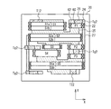

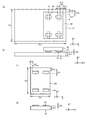


Classifications
-
- H—ELECTRICITY
- H03—ELECTRONIC CIRCUITRY
- H03H—IMPEDANCE NETWORKS, e.g. RESONANT CIRCUITS; RESONATORS
- H03H9/00—Networks comprising electromechanical or electro-acoustic elements; Electromechanical resonators
- H03H9/02—Details
- H03H9/05—Holders or supports
- H03H9/058—Holders or supports for surface acoustic wave devices
- H03H9/059—Holders or supports for surface acoustic wave devices consisting of mounting pads or bumps
-
- H—ELECTRICITY
- H03—ELECTRONIC CIRCUITRY
- H03H—IMPEDANCE NETWORKS, e.g. RESONANT CIRCUITS; RESONATORS
- H03H3/00—Apparatus or processes specially adapted for the manufacture of impedance networks, resonating circuits, resonators
- H03H3/007—Apparatus or processes specially adapted for the manufacture of impedance networks, resonating circuits, resonators for the manufacture of electromechanical resonators or networks
- H03H3/08—Apparatus or processes specially adapted for the manufacture of impedance networks, resonating circuits, resonators for the manufacture of electromechanical resonators or networks for the manufacture of resonators or networks using surface acoustic waves
-
- H—ELECTRICITY
- H03—ELECTRONIC CIRCUITRY
- H03H—IMPEDANCE NETWORKS, e.g. RESONANT CIRCUITS; RESONATORS
- H03H9/00—Networks comprising electromechanical or electro-acoustic elements; Electromechanical resonators
- H03H9/25—Constructional features of resonators using surface acoustic waves
-
- H—ELECTRICITY
- H10—SEMICONDUCTOR DEVICES; ELECTRIC SOLID-STATE DEVICES NOT OTHERWISE PROVIDED FOR
- H10N—ELECTRIC SOLID-STATE DEVICES NOT OTHERWISE PROVIDED FOR
- H10N30/00—Piezoelectric or electrostrictive devices
- H10N30/01—Manufacture or treatment
- H10N30/07—Forming of piezoelectric or electrostrictive parts or bodies on an electrical element or another base
- H10N30/072—Forming of piezoelectric or electrostrictive parts or bodies on an electrical element or another base by laminating or bonding of piezoelectric or electrostrictive bodies
- H10N30/073—Forming of piezoelectric or electrostrictive parts or bodies on an electrical element or another base by laminating or bonding of piezoelectric or electrostrictive bodies by fusion of metals or by adhesives
-
- H—ELECTRICITY
- H10—SEMICONDUCTOR DEVICES; ELECTRIC SOLID-STATE DEVICES NOT OTHERWISE PROVIDED FOR
- H10N—ELECTRIC SOLID-STATE DEVICES NOT OTHERWISE PROVIDED FOR
- H10N30/00—Piezoelectric or electrostrictive devices
- H10N30/80—Constructional details
- H10N30/85—Piezoelectric or electrostrictive active materials
- H10N30/853—Ceramic compositions
- H10N30/8542—Alkali metal based oxides, e.g. lithium, sodium or potassium niobates
-
- H—ELECTRICITY
- H10—SEMICONDUCTOR DEVICES; ELECTRIC SOLID-STATE DEVICES NOT OTHERWISE PROVIDED FOR
- H10N—ELECTRIC SOLID-STATE DEVICES NOT OTHERWISE PROVIDED FOR
- H10N30/00—Piezoelectric or electrostrictive devices
- H10N30/80—Constructional details
- H10N30/88—Mounts; Supports; Enclosures; Casings
- H10N30/883—Additional insulation means preventing electrical, physical or chemical damage, e.g. protective coatings
-
- H—ELECTRICITY
- H03—ELECTRONIC CIRCUITRY
- H03H—IMPEDANCE NETWORKS, e.g. RESONANT CIRCUITS; RESONATORS
- H03H9/00—Networks comprising electromechanical or electro-acoustic elements; Electromechanical resonators
- H03H9/46—Filters
- H03H9/64—Filters using surface acoustic waves
- H03H9/6423—Means for obtaining a particular transfer characteristic
- H03H9/6433—Coupled resonator filters
- H03H9/6483—Ladder SAW filters
-
- H—ELECTRICITY
- H10—SEMICONDUCTOR DEVICES; ELECTRIC SOLID-STATE DEVICES NOT OTHERWISE PROVIDED FOR
- H10N—ELECTRIC SOLID-STATE DEVICES NOT OTHERWISE PROVIDED FOR
- H10N30/00—Piezoelectric or electrostrictive devices
- H10N30/80—Constructional details
- H10N30/87—Electrodes or interconnections, e.g. leads or terminals
-
- H—ELECTRICITY
- H10—SEMICONDUCTOR DEVICES; ELECTRIC SOLID-STATE DEVICES NOT OTHERWISE PROVIDED FOR
- H10W—GENERIC PACKAGES, INTERCONNECTIONS, CONNECTORS OR OTHER CONSTRUCTIONAL DETAILS OF DEVICES COVERED BY CLASS H10
- H10W70/00—Package substrates; Interposers; Redistribution layers [RDL]
- H10W70/60—Insulating or insulated package substrates; Interposers; Redistribution layers
- H10W70/62—Insulating or insulated package substrates; Interposers; Redistribution layers characterised by their interconnections
- H10W70/65—Shapes or dispositions of interconnections
- H10W70/654—Top-view layouts
- H10W70/655—Fan-out layouts
-
- H—ELECTRICITY
- H10—SEMICONDUCTOR DEVICES; ELECTRIC SOLID-STATE DEVICES NOT OTHERWISE PROVIDED FOR
- H10W—GENERIC PACKAGES, INTERCONNECTIONS, CONNECTORS OR OTHER CONSTRUCTIONAL DETAILS OF DEVICES COVERED BY CLASS H10
- H10W90/00—Package configurations
- H10W90/701—Package configurations characterised by the relative positions of pads or connectors relative to package parts
- H10W90/721—Package configurations characterised by the relative positions of pads or connectors relative to package parts of bump connectors
- H10W90/724—Package configurations characterised by the relative positions of pads or connectors relative to package parts of bump connectors between a chip and a stacked insulating package substrate, interposer or RDL
Landscapes
- Physics & Mathematics (AREA)
- Acoustics & Sound (AREA)
- Engineering & Computer Science (AREA)
- Manufacturing & Machinery (AREA)
- Chemical & Material Sciences (AREA)
- Materials Engineering (AREA)
- Ceramic Engineering (AREA)
- Surface Acoustic Wave Elements And Circuit Networks Thereof (AREA)
Priority Applications (2)
| Application Number | Priority Date | Filing Date | Title |
|---|---|---|---|
| JP2016174064A JP6590772B2 (ja) | 2016-09-06 | 2016-09-06 | 弾性波デバイスとその製造方法 |
| US15/686,621 US11271542B2 (en) | 2016-09-06 | 2017-08-25 | Acoustic wave device and method of fabricating the same |
Applications Claiming Priority (1)
| Application Number | Priority Date | Filing Date | Title |
|---|---|---|---|
| JP2016174064A JP6590772B2 (ja) | 2016-09-06 | 2016-09-06 | 弾性波デバイスとその製造方法 |
Publications (3)
| Publication Number | Publication Date |
|---|---|
| JP2018042072A JP2018042072A (ja) | 2018-03-15 |
| JP2018042072A5 JP2018042072A5 (enExample) | 2018-04-26 |
| JP6590772B2 true JP6590772B2 (ja) | 2019-10-16 |
Family
ID=61280945
Family Applications (1)
| Application Number | Title | Priority Date | Filing Date |
|---|---|---|---|
| JP2016174064A Expired - Fee Related JP6590772B2 (ja) | 2016-09-06 | 2016-09-06 | 弾性波デバイスとその製造方法 |
Country Status (2)
| Country | Link |
|---|---|
| US (1) | US11271542B2 (enExample) |
| JP (1) | JP6590772B2 (enExample) |
Families Citing this family (3)
| Publication number | Priority date | Publication date | Assignee | Title |
|---|---|---|---|---|
| JP7541324B2 (ja) * | 2020-04-13 | 2024-08-28 | 三安ジャパンテクノロジー株式会社 | 弾性波デバイスパッケージ |
| US12199584B2 (en) | 2021-04-16 | 2025-01-14 | Murata Manufacturing Co., Ltd. | Transversely-excited film bulk acoustic resonator fabrication using wafer-to-wafer bonding |
| US12308818B2 (en) * | 2023-01-03 | 2025-05-20 | Win Semiconductors Corp. | Surface acoustic wave device |
Family Cites Families (10)
| Publication number | Priority date | Publication date | Assignee | Title |
|---|---|---|---|---|
| JPH1079638A (ja) | 1996-09-05 | 1998-03-24 | Oki Electric Ind Co Ltd | 表面弾性波フィルタ及びその製造方法 |
| JP2004304622A (ja) | 2003-03-31 | 2004-10-28 | Fujitsu Media Device Kk | 弾性表面波デバイス及びその製造方法 |
| JP2005026630A (ja) | 2003-07-03 | 2005-01-27 | Nec Electronics Corp | 半導体装置及びその製造方法 |
| JP2006319211A (ja) | 2005-05-13 | 2006-11-24 | Sharp Corp | 半導体チップの実装構造 |
| JP5686943B2 (ja) * | 2008-09-17 | 2015-03-18 | 太陽誘電株式会社 | 弾性波デバイス及びその製造方法 |
| WO2013078438A1 (en) * | 2011-11-23 | 2013-05-30 | Microvention, Inc. | Embolic device with shaped wire |
| JP2013121711A (ja) * | 2011-12-12 | 2013-06-20 | Canon Inc | 記録装置、および記録方法 |
| JP2013131711A (ja) * | 2011-12-22 | 2013-07-04 | Taiyo Yuden Co Ltd | 電子部品 |
| JP6106404B2 (ja) * | 2012-10-30 | 2017-03-29 | 太陽誘電株式会社 | 電子部品モジュール |
| JP6472945B2 (ja) * | 2013-06-13 | 2019-02-20 | 太陽誘電株式会社 | 弾性波デバイス |
-
2016
- 2016-09-06 JP JP2016174064A patent/JP6590772B2/ja not_active Expired - Fee Related
-
2017
- 2017-08-25 US US15/686,621 patent/US11271542B2/en active Active
Also Published As
| Publication number | Publication date |
|---|---|
| JP2018042072A (ja) | 2018-03-15 |
| US20180069526A1 (en) | 2018-03-08 |
| US11271542B2 (en) | 2022-03-08 |
Similar Documents
| Publication | Publication Date | Title |
|---|---|---|
| JP6454299B2 (ja) | 弾性波デバイス | |
| JP6556663B2 (ja) | 弾性波デバイス | |
| JP6461036B2 (ja) | 弾性波デバイス | |
| JP4377500B2 (ja) | 弾性表面波装置及び弾性表面波装置の製造方法 | |
| JP6801783B2 (ja) | 電子部品およびそれを備えるモジュール | |
| JP6315650B2 (ja) | 電子デバイス | |
| JP7231360B2 (ja) | 弾性波デバイス | |
| JP2019125871A (ja) | 弾性波装置 | |
| JP6430977B2 (ja) | 弾性波デバイス | |
| JP6963445B2 (ja) | 電子部品 | |
| JP3913700B2 (ja) | 弾性表面波デバイス及びその製造方法 | |
| WO2016199645A1 (ja) | 圧電振動デバイス | |
| JP6433930B2 (ja) | 弾性波デバイス | |
| KR20010081032A (ko) | 탄성 표면파 디바이스 및 그 제조방법 | |
| JP2019021998A (ja) | 電子部品 | |
| JP2018125773A (ja) | 弾性波デバイス | |
| JP7370146B2 (ja) | 弾性波デバイス、フィルタおよびマルチプレクサ | |
| CN109494212B (zh) | 电子部件 | |
| JP2018042072A (ja) | 弾性波デバイスとその製造方法 | |
| JP2018101955A (ja) | 弾性波デバイス | |
| JP6733492B2 (ja) | 圧電振動デバイス | |
| JP2018042072A5 (enExample) | ||
| JP4722204B2 (ja) | 弾性表面波装置及び弾性表面波装置の製造方法 | |
| JP6793009B2 (ja) | 弾性波デバイス及び多面取り基板 | |
| JP7577535B2 (ja) | 電子部品 |
Legal Events
| Date | Code | Title | Description |
|---|---|---|---|
| A521 | Request for written amendment filed |
Free format text: JAPANESE INTERMEDIATE CODE: A523 Effective date: 20180305 |
|
| A621 | Written request for application examination |
Free format text: JAPANESE INTERMEDIATE CODE: A621 Effective date: 20180305 |
|
| A977 | Report on retrieval |
Free format text: JAPANESE INTERMEDIATE CODE: A971007 Effective date: 20190212 |
|
| A131 | Notification of reasons for refusal |
Free format text: JAPANESE INTERMEDIATE CODE: A131 Effective date: 20190305 |
|
| A521 | Request for written amendment filed |
Free format text: JAPANESE INTERMEDIATE CODE: A523 Effective date: 20190417 |
|
| TRDD | Decision of grant or rejection written | ||
| A01 | Written decision to grant a patent or to grant a registration (utility model) |
Free format text: JAPANESE INTERMEDIATE CODE: A01 Effective date: 20190820 |
|
| A61 | First payment of annual fees (during grant procedure) |
Free format text: JAPANESE INTERMEDIATE CODE: A61 Effective date: 20190917 |
|
| R150 | Certificate of patent or registration of utility model |
Ref document number: 6590772 Country of ref document: JP Free format text: JAPANESE INTERMEDIATE CODE: R150 |
|
| R250 | Receipt of annual fees |
Free format text: JAPANESE INTERMEDIATE CODE: R250 |
|
| R250 | Receipt of annual fees |
Free format text: JAPANESE INTERMEDIATE CODE: R250 |
|
| LAPS | Cancellation because of no payment of annual fees |