JP6495291B2 - 集積回路の静電放電保護 - Google Patents
集積回路の静電放電保護 Download PDFInfo
- Publication number
- JP6495291B2 JP6495291B2 JP2016542015A JP2016542015A JP6495291B2 JP 6495291 B2 JP6495291 B2 JP 6495291B2 JP 2016542015 A JP2016542015 A JP 2016542015A JP 2016542015 A JP2016542015 A JP 2016542015A JP 6495291 B2 JP6495291 B2 JP 6495291B2
- Authority
- JP
- Japan
- Prior art keywords
- diode
- drain
- gate
- voltage
- input transistor
- Prior art date
- Legal status (The legal status is an assumption and is not a legal conclusion. Google has not performed a legal analysis and makes no representation as to the accuracy of the status listed.)
- Expired - Fee Related
Links
Images

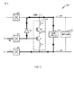
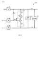


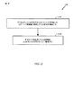

Classifications
-
- H—ELECTRICITY
- H10—SEMICONDUCTOR DEVICES; ELECTRIC SOLID-STATE DEVICES NOT OTHERWISE PROVIDED FOR
- H10D—INORGANIC ELECTRIC SEMICONDUCTOR DEVICES
- H10D89/00—Aspects of integrated devices not covered by groups H10D84/00 - H10D88/00
- H10D89/60—Integrated devices comprising arrangements for electrical or thermal protection, e.g. protection circuits against electrostatic discharge [ESD]
- H10D89/601—Integrated devices comprising arrangements for electrical or thermal protection, e.g. protection circuits against electrostatic discharge [ESD] for devices having insulated gate electrodes, e.g. for IGFETs or IGBTs
- H10D89/611—Integrated devices comprising arrangements for electrical or thermal protection, e.g. protection circuits against electrostatic discharge [ESD] for devices having insulated gate electrodes, e.g. for IGFETs or IGBTs using diodes as protective elements
-
- H—ELECTRICITY
- H02—GENERATION; CONVERSION OR DISTRIBUTION OF ELECTRIC POWER
- H02H—EMERGENCY PROTECTIVE CIRCUIT ARRANGEMENTS
- H02H9/00—Emergency protective circuit arrangements for limiting excess current or voltage without disconnection
- H02H9/04—Emergency protective circuit arrangements for limiting excess current or voltage without disconnection responsive to excess voltage
- H02H9/045—Emergency protective circuit arrangements for limiting excess current or voltage without disconnection responsive to excess voltage adapted to a particular application and not provided for elsewhere
- H02H9/046—Emergency protective circuit arrangements for limiting excess current or voltage without disconnection responsive to excess voltage adapted to a particular application and not provided for elsewhere responsive to excess voltage appearing at terminals of integrated circuits
-
- H—ELECTRICITY
- H03—ELECTRONIC CIRCUITRY
- H03F—AMPLIFIERS
- H03F1/00—Details of amplifiers with only discharge tubes, only semiconductor devices or only unspecified devices as amplifying elements
- H03F1/08—Modifications of amplifiers to reduce detrimental influences of internal impedances of amplifying elements
- H03F1/22—Modifications of amplifiers to reduce detrimental influences of internal impedances of amplifying elements by use of cascode coupling, i.e. earthed cathode or emitter stage followed by earthed grid or base stage respectively
- H03F1/223—Modifications of amplifiers to reduce detrimental influences of internal impedances of amplifying elements by use of cascode coupling, i.e. earthed cathode or emitter stage followed by earthed grid or base stage respectively with MOSFET's
-
- H—ELECTRICITY
- H03—ELECTRONIC CIRCUITRY
- H03F—AMPLIFIERS
- H03F1/00—Details of amplifiers with only discharge tubes, only semiconductor devices or only unspecified devices as amplifying elements
- H03F1/52—Circuit arrangements for protecting such amplifiers
- H03F1/523—Circuit arrangements for protecting such amplifiers for amplifiers using field-effect devices
-
- H—ELECTRICITY
- H03—ELECTRONIC CIRCUITRY
- H03F—AMPLIFIERS
- H03F2200/00—Indexing scheme relating to amplifiers
- H03F2200/336—A I/Q, i.e. phase quadrature, modulator or demodulator being used in an amplifying circuit
-
- H—ELECTRICITY
- H03—ELECTRONIC CIRCUITRY
- H03F—AMPLIFIERS
- H03F2200/00—Indexing scheme relating to amplifiers
- H03F2200/429—Two or more amplifiers or one amplifier with filters for different frequency bands are coupled in parallel at the input or output
-
- H—ELECTRICITY
- H03—ELECTRONIC CIRCUITRY
- H03F—AMPLIFIERS
- H03F2200/00—Indexing scheme relating to amplifiers
- H03F2200/441—Protection of an amplifier being implemented by clamping means
-
- H—ELECTRICITY
- H03—ELECTRONIC CIRCUITRY
- H03F—AMPLIFIERS
- H03F2200/00—Indexing scheme relating to amplifiers
- H03F2200/444—Diode used as protection means in an amplifier, e.g. as a limiter or as a switch
Landscapes
- Engineering & Computer Science (AREA)
- Power Engineering (AREA)
- Microelectronics & Electronic Packaging (AREA)
- Semiconductor Integrated Circuits (AREA)
- Amplifiers (AREA)
Applications Claiming Priority (3)
| Application Number | Priority Date | Filing Date | Title |
|---|---|---|---|
| US14/024,833 | 2013-09-12 | ||
| US14/024,833 US9608437B2 (en) | 2013-09-12 | 2013-09-12 | Electro-static discharge protection for integrated circuits |
| PCT/US2014/054104 WO2015038402A1 (en) | 2013-09-12 | 2014-09-04 | Electro-static discharge protection for integrated circuits |
Publications (3)
| Publication Number | Publication Date |
|---|---|
| JP2016534577A JP2016534577A (ja) | 2016-11-04 |
| JP2016534577A5 JP2016534577A5 (enExample) | 2017-09-21 |
| JP6495291B2 true JP6495291B2 (ja) | 2019-04-03 |
Family
ID=51541383
Family Applications (1)
| Application Number | Title | Priority Date | Filing Date |
|---|---|---|---|
| JP2016542015A Expired - Fee Related JP6495291B2 (ja) | 2013-09-12 | 2014-09-04 | 集積回路の静電放電保護 |
Country Status (6)
| Country | Link |
|---|---|
| US (1) | US9608437B2 (enExample) |
| EP (1) | EP3044810B1 (enExample) |
| JP (1) | JP6495291B2 (enExample) |
| KR (1) | KR20160055201A (enExample) |
| CN (1) | CN105556666B (enExample) |
| WO (1) | WO2015038402A1 (enExample) |
Families Citing this family (14)
| Publication number | Priority date | Publication date | Assignee | Title |
|---|---|---|---|---|
| EP3118992A1 (en) * | 2015-07-16 | 2017-01-18 | Nxp B.V. | An rf amplifier |
| GB2572711A (en) * | 2017-02-22 | 2019-10-09 | Mitsubishi Electric Corp | High frequency amplifier |
| JP6761374B2 (ja) * | 2017-05-25 | 2020-09-23 | 株式会社東芝 | 半導体装置 |
| CN110138375B (zh) * | 2018-02-02 | 2021-08-27 | 华为技术有限公司 | 一种用于芯片管脚的电路 |
| DE102019121271A1 (de) * | 2018-08-30 | 2020-03-05 | Taiwan Semiconductor Manufacturing Company, Ltd. | ESD-Schutzschaltung, Halbleitersystem, das diese aufweist, und Verfahren zum Betreiben derselben |
| US11774561B2 (en) | 2019-02-08 | 2023-10-03 | Luminar Technologies, Inc. | Amplifier input protection circuits |
| CN109830478B (zh) * | 2019-02-19 | 2021-05-04 | 杭州晶华微电子股份有限公司 | 一种超低漏电流的芯片输入引脚esd保护电路架构 |
| TWI756639B (zh) * | 2020-02-26 | 2022-03-01 | 瑞昱半導體股份有限公司 | 支援消費性電子產品控制通訊協定之控制晶片與相關的耐高壓輸出電路 |
| TWI753751B (zh) * | 2021-01-19 | 2022-01-21 | 旺宏電子股份有限公司 | 靜電放電保護裝置及其操作方法 |
| WO2022218392A1 (zh) * | 2021-04-14 | 2022-10-20 | 南方科技大学 | 静电放电esd保护电路 |
| CN118648236A (zh) * | 2022-02-04 | 2024-09-13 | Qorvo美国公司 | 用于功率放大器的偏置电路 |
| US12034000B2 (en) * | 2022-03-23 | 2024-07-09 | Nxp B.V. | Double IO pad cell including electrostatic discharge protection scheme with reduced latch-up risk |
| US20250286518A1 (en) * | 2024-03-11 | 2025-09-11 | Psemi Corporation | ESD Protection Circuit |
| CN121585100B (zh) * | 2026-01-29 | 2026-07-10 | 成都嘉纳海威科技有限责任公司 | 一种增益可调且具管芯保护功能的宽带放大器电路 |
Family Cites Families (40)
| Publication number | Priority date | Publication date | Assignee | Title |
|---|---|---|---|---|
| US4683443A (en) * | 1986-01-27 | 1987-07-28 | The United States Of America As Represented By The Secretary Of The Air Force | Monolithic low noise amplifier with limiting |
| US5005061A (en) * | 1990-02-05 | 1991-04-02 | Motorola, Inc. | Avalanche stress protected semiconductor device having variable input impedance |
| GB9115699D0 (en) * | 1991-07-19 | 1991-09-04 | Philips Electronic Associated | An overvoltage protected semiconductor switch |
| US5521783A (en) * | 1993-09-17 | 1996-05-28 | Analog Devices, Inc. | Electrostatic discharge protection circuit |
| US5589799A (en) * | 1994-09-29 | 1996-12-31 | Tibbetts Industries, Inc. | Low noise amplifier for microphone |
| JP3805543B2 (ja) * | 1998-11-19 | 2006-08-02 | 三菱電機株式会社 | 半導体集積回路 |
| US6249410B1 (en) * | 1999-08-23 | 2001-06-19 | Taiwan Semiconductor Manufacturing Company | ESD protection circuit without overstress gate-driven effect |
| JP2001358297A (ja) * | 2000-06-14 | 2001-12-26 | Nec Corp | 静電保護回路 |
| EP1217662A1 (en) * | 2000-12-21 | 2002-06-26 | Universite Catholique De Louvain | Ultra-low power basic blocks and their uses |
| US6617649B2 (en) | 2000-12-28 | 2003-09-09 | Industrial Technology Research Institute | Low substrate-noise electrostatic discharge protection circuits with bi-directional silicon diodes |
| US6894567B2 (en) * | 2001-12-04 | 2005-05-17 | Koninklijke Philips Electronics N.V. | ESD protection circuit for use in RF CMOS IC design |
| US20050045952A1 (en) * | 2003-08-27 | 2005-03-03 | International Business Machines Corporation | Pfet-based esd protection strategy for improved external latch-up robustness |
| JP2008502300A (ja) * | 2004-06-08 | 2008-01-24 | サーノフ コーポレーション | 電流制御型静電放電保護を提供する方法および装置 |
| US7336459B2 (en) * | 2004-07-29 | 2008-02-26 | United Microelectronics Corp. | Electrostatic discharge protection device and circuit thereof |
| JP2008514010A (ja) * | 2004-09-16 | 2008-05-01 | サーノフ コーポレーション | Esd保護用の装置 |
| US7145204B2 (en) * | 2005-04-15 | 2006-12-05 | Texas Instruments Incorporated | Guardwall structures for ESD protection |
| US7649722B2 (en) | 2005-09-14 | 2010-01-19 | Interuniversitair Microelektronica Centrum (Imec) | Electrostatic discharge protected circuits |
| US7382593B2 (en) * | 2005-09-14 | 2008-06-03 | Fairchild Semiconductor | Method of linearizing ESD capacitance |
| DE102006019888B4 (de) * | 2006-04-28 | 2012-10-04 | Infineon Technologies Ag | Verstärker mit ESD-Schutz |
| US7593204B1 (en) | 2006-06-06 | 2009-09-22 | Rf Micro Devices, Inc. | On-chip ESD protection circuit for radio frequency (RF) integrated circuits |
| US7848068B2 (en) * | 2006-09-07 | 2010-12-07 | Industrial Technology Research Institute | ESD protection circuit using self-biased current trigger technique and pumping source mechanism |
| US7583034B2 (en) * | 2006-09-26 | 2009-09-01 | Semiconductor Components Industries, L.L.C. | LED controller and method therefor |
| CN101287304B (zh) * | 2006-12-18 | 2013-02-06 | 桑尼奥公司 | 具有厚氧化物输入级晶体管的深亚微米mos前置放大器 |
| KR20080076411A (ko) * | 2007-02-15 | 2008-08-20 | 주식회사 하이닉스반도체 | 정전기 보호 회로 |
| JP4303761B2 (ja) * | 2007-03-07 | 2009-07-29 | Necエレクトロニクス株式会社 | 半導体回路及びその動作方法 |
| KR100878439B1 (ko) * | 2007-08-30 | 2009-01-13 | 주식회사 실리콘웍스 | 출력 드라이버단의 esd 보호 장치 |
| JP2010103274A (ja) * | 2008-10-23 | 2010-05-06 | Nec Electronics Corp | 半導体パッケージ |
| US8089873B2 (en) * | 2008-10-28 | 2012-01-03 | Kyungpook National University Industry-Academic Cooperation Foundation | Method and system of managing QoS-guaranteed multimode fast mobility in wireless networks |
| US8213142B2 (en) * | 2008-10-29 | 2012-07-03 | Qualcomm, Incorporated | Amplifier with improved ESD protection circuitry |
| US8331068B2 (en) | 2009-02-19 | 2012-12-11 | Taiwan Semiconductor Manufacturing Company, Ltd. | ESD protection for FinFETs |
| TWI463792B (zh) * | 2009-10-29 | 2014-12-01 | Novatek Microelectronics Corp | 具有過衝抑制功能的放大電路 |
| US8482888B2 (en) * | 2010-05-20 | 2013-07-09 | Taiwan Semiconductor Manufacturing Co. Ltd. | ESD block with shared noise optimization and CDM ESD protection for RF circuits |
| US8564917B2 (en) * | 2011-06-02 | 2013-10-22 | GlobalFoundries, Inc. | Integrated circuit having electrostatic discharge protection |
| JP5896682B2 (ja) * | 2011-10-18 | 2016-03-30 | ルネサスエレクトロニクス株式会社 | 半導体集積回路装置 |
| FR2982416B1 (fr) * | 2011-11-03 | 2014-01-03 | St Microelectronics Sa | Dispositif electronique de protection contre les decharges electrostatiques |
| KR20130072090A (ko) * | 2011-12-21 | 2013-07-01 | 에스케이하이닉스 주식회사 | 반도체 집적회로 |
| EP2677540A1 (en) * | 2012-06-19 | 2013-12-25 | Nxp B.V. | Electronic device and method of manufacturing the same |
| US9590571B2 (en) * | 2012-10-02 | 2017-03-07 | Knowles Electronics, Llc | Single stage buffer with filter |
| US9929698B2 (en) * | 2013-03-15 | 2018-03-27 | Qualcomm Incorporated | Radio frequency integrated circuit (RFIC) charged-device model (CDM) protection |
| US20140268446A1 (en) * | 2013-03-15 | 2014-09-18 | Qualcomm Incorporated | Radio frequency integrated circuit (rfic) charged-device model (cdm) protection |
-
2013
- 2013-09-12 US US14/024,833 patent/US9608437B2/en active Active
-
2014
- 2014-09-04 WO PCT/US2014/054104 patent/WO2015038402A1/en not_active Ceased
- 2014-09-04 KR KR1020167009193A patent/KR20160055201A/ko not_active Withdrawn
- 2014-09-04 JP JP2016542015A patent/JP6495291B2/ja not_active Expired - Fee Related
- 2014-09-04 EP EP14766354.6A patent/EP3044810B1/en active Active
- 2014-09-04 CN CN201480049879.7A patent/CN105556666B/zh active Active
Also Published As
| Publication number | Publication date |
|---|---|
| US9608437B2 (en) | 2017-03-28 |
| CN105556666B (zh) | 2018-11-06 |
| EP3044810A1 (en) | 2016-07-20 |
| WO2015038402A1 (en) | 2015-03-19 |
| KR20160055201A (ko) | 2016-05-17 |
| JP2016534577A (ja) | 2016-11-04 |
| CN105556666A (zh) | 2016-05-04 |
| US20150070803A1 (en) | 2015-03-12 |
| EP3044810B1 (en) | 2020-11-11 |
Similar Documents
| Publication | Publication Date | Title |
|---|---|---|
| EP3044810B1 (en) | Electro-static discharge protection for integrated circuits | |
| JP6584955B2 (ja) | 増幅器カスコードデバイスの静電放電保護 | |
| KR101346543B1 (ko) | 개선된 esd 보호 회로를 갖는 증폭기 | |
| JP5437534B2 (ja) | エリア効率の良い同時整合トランシーバ | |
| CN110311630A (zh) | 用于旁路低噪声放大器的系统和方法 | |
| WO2019078994A1 (en) | PROTECTION AGAINST THE REINFORCED BY A PASSIVE EQUALIZATION T-COIL | |
| TWI279903B (en) | ESD protection circuit for use in RF CMOS IC design | |
| JP2016501501A5 (enExample) | ||
| CN102474246A (zh) | 具有可变控制电压的开关 | |
| CN104185955A (zh) | 具有集成rx/tx可配置无源网络的收发器 | |
| KR101770786B1 (ko) | 무선 트랜시버의 송수신 스위치 | |
| US9425853B2 (en) | Amplifier utilizing a configurable interface to a front end module | |
| US8643427B2 (en) | Switching device | |
| US11005173B2 (en) | ESD protection for antenna port | |
| JP5743983B2 (ja) | 送受切替回路、無線装置および送受切替方法 | |
| CN105097799A (zh) | 信号接收电路和信号收发电路 | |
| US20170092637A1 (en) | Semiconductor ESD Protection Device and Method | |
| JP2015154485A (ja) | 増幅回路の帯域幅を改善するための方法及び回路 | |
| JP5348050B2 (ja) | 雑音発生回路及び受信回路 | |
| CN115882878A (zh) | 支持天线分集的发射机设备 | |
| JP2015154483A (ja) | 受信回路、光受信機及びリターンロス削減方法 | |
| EP3732544B1 (en) | Voltage protection circuit | |
| US20250175202A1 (en) | Switch circuits, attenuation circuits, receivers, base station and mobile device | |
| JP2015062268A (ja) | 無線周波数通信システム及びその無線周波数通信システムに応用されるノイズアイソレーション方法 | |
| US8937501B1 (en) | Active field effect transistor limiter |
Legal Events
| Date | Code | Title | Description |
|---|---|---|---|
| A521 | Request for written amendment filed |
Free format text: JAPANESE INTERMEDIATE CODE: A523 Effective date: 20170808 |
|
| A621 | Written request for application examination |
Free format text: JAPANESE INTERMEDIATE CODE: A621 Effective date: 20170808 |
|
| A977 | Report on retrieval |
Free format text: JAPANESE INTERMEDIATE CODE: A971007 Effective date: 20180427 |
|
| A131 | Notification of reasons for refusal |
Free format text: JAPANESE INTERMEDIATE CODE: A131 Effective date: 20180508 |
|
| A601 | Written request for extension of time |
Free format text: JAPANESE INTERMEDIATE CODE: A601 Effective date: 20180808 |
|
| A521 | Request for written amendment filed |
Free format text: JAPANESE INTERMEDIATE CODE: A523 Effective date: 20180829 |
|
| TRDD | Decision of grant or rejection written | ||
| A01 | Written decision to grant a patent or to grant a registration (utility model) |
Free format text: JAPANESE INTERMEDIATE CODE: A01 Effective date: 20190205 |
|
| A61 | First payment of annual fees (during grant procedure) |
Free format text: JAPANESE INTERMEDIATE CODE: A61 Effective date: 20190306 |
|
| R150 | Certificate of patent or registration of utility model |
Ref document number: 6495291 Country of ref document: JP Free format text: JAPANESE INTERMEDIATE CODE: R150 |
|
| LAPS | Cancellation because of no payment of annual fees |