US5589799A - Low noise amplifier for microphone - Google Patents
Low noise amplifier for microphone Download PDFInfo
- Publication number
- US5589799A US5589799A US08/447,349 US44734995A US5589799A US 5589799 A US5589799 A US 5589799A US 44734995 A US44734995 A US 44734995A US 5589799 A US5589799 A US 5589799A
- Authority
- US
- United States
- Prior art keywords
- jfet
- stage
- source
- gate
- ground
- Prior art date
- Legal status (The legal status is an assumption and is not a legal conclusion. Google has not performed a legal analysis and makes no representation as to the accuracy of the status listed.)
- Expired - Fee Related
Links
- 239000003990 capacitor Substances 0.000 claims abstract description 15
- 238000007493 shaping process Methods 0.000 claims abstract description 5
- 230000008878 coupling Effects 0.000 claims description 7
- 238000010168 coupling process Methods 0.000 claims description 7
- 238000005859 coupling reaction Methods 0.000 claims description 7
- 230000004044 response Effects 0.000 claims description 5
- 230000001681 protective effect Effects 0.000 claims description 2
- 230000005669 field effect Effects 0.000 abstract description 11
- 230000009467 reduction Effects 0.000 description 5
- 230000003321 amplification Effects 0.000 description 4
- 238000003199 nucleic acid amplification method Methods 0.000 description 4
- 230000007423 decrease Effects 0.000 description 3
- 230000006872 improvement Effects 0.000 description 3
- 239000004065 semiconductor Substances 0.000 description 3
- 230000009286 beneficial effect Effects 0.000 description 2
- 230000001939 inductive effect Effects 0.000 description 2
- 230000005534 acoustic noise Effects 0.000 description 1
- 230000008901 benefit Effects 0.000 description 1
- 239000000872 buffer Substances 0.000 description 1
- 238000006243 chemical reaction Methods 0.000 description 1
- 238000013016 damping Methods 0.000 description 1
- 230000003247 decreasing effect Effects 0.000 description 1
- 230000000694 effects Effects 0.000 description 1
- 238000001914 filtration Methods 0.000 description 1
- 230000006870 function Effects 0.000 description 1
- 230000010354 integration Effects 0.000 description 1
- 229910044991 metal oxide Inorganic materials 0.000 description 1
- 150000004706 metal oxides Chemical class 0.000 description 1
Images
Classifications
-
- H—ELECTRICITY
- H03—ELECTRONIC CIRCUITRY
- H03F—AMPLIFIERS
- H03F3/00—Amplifiers with only discharge tubes or only semiconductor devices as amplifying elements
- H03F3/181—Low-frequency amplifiers, e.g. audio preamplifiers
- H03F3/183—Low-frequency amplifiers, e.g. audio preamplifiers with semiconductor devices only
- H03F3/185—Low-frequency amplifiers, e.g. audio preamplifiers with semiconductor devices only with field-effect devices
- H03F3/1855—Low-frequency amplifiers, e.g. audio preamplifiers with semiconductor devices only with field-effect devices with junction-FET devices
-
- H—ELECTRICITY
- H03—ELECTRONIC CIRCUITRY
- H03F—AMPLIFIERS
- H03F2200/00—Indexing scheme relating to amplifiers
- H03F2200/03—Indexing scheme relating to amplifiers the amplifier being designed for audio applications
-
- H—ELECTRICITY
- H03—ELECTRONIC CIRCUITRY
- H03F—AMPLIFIERS
- H03F2200/00—Indexing scheme relating to amplifiers
- H03F2200/372—Noise reduction and elimination in amplifier
-
- H—ELECTRICITY
- H03—ELECTRONIC CIRCUITRY
- H03F—AMPLIFIERS
- H03F2200/00—Indexing scheme relating to amplifiers
- H03F2200/54—Two or more capacitor coupled amplifier stages in cascade
-
- H—ELECTRICITY
- H04—ELECTRIC COMMUNICATION TECHNIQUE
- H04R—LOUDSPEAKERS, MICROPHONES, GRAMOPHONE PICK-UPS OR LIKE ACOUSTIC ELECTROMECHANICAL TRANSDUCERS; DEAF-AID SETS; PUBLIC ADDRESS SYSTEMS
- H04R25/00—Deaf-aid sets, i.e. electro-acoustic or electro-mechanical hearing aids; Electric tinnitus maskers providing an auditory perception
- H04R25/50—Customised settings for obtaining desired overall acoustical characteristics
- H04R25/502—Customised settings for obtaining desired overall acoustical characteristics using analog signal processing
Definitions
- This invention relates generally to audio frequency amplification circuits used as the preamplifier stages of microphone transducers. More particularly, the invention relates to circuits employing field effect transistors operating with low voltage sources, suitable for use with electret based condenser microphones.
- the signal-to-noise ratio for electret based condenser microphones has not significantly improved in the past 25 years. During that time there has been a decrease in transducer size, with the signal-to-noise ratio either remaining the same or, in the case of the later smaller transducers, actually declining along with the signal.
- JFET N channel junction field effect transistor
- U.S. Pat. No. 4,151,480 issued on Apr. 24, 1979 to Carlson et al discloses an amplification circuit employing, in addition to a field effect transistor connected in follower mode, a second field effect transistor used as a current source in lieu of a source resistor, thus providing a much higher ac load impedance than would a simple resistor with the same dc current flowing through it.
- U.S. Pat. No. 3,512,100 issued May 12, 1970 to Burkhard et al discloses a pair of diodes of opposite polarity connected in parallel as the gate bias of a field effect transistor connected in follower mode.
- a resistor of large impedance used for gate bias can introduce noise at low frequencies (up to about 1000 Hz)
- the use of diodes dramatically reduces noise at those frequencies because the diodes act as resistors of very much larger values.
- such diodes can be prone to failure due to electrostatic discharge.
- U.S. Pat. No. 5,083,095 issued Jan. 21, 1992 to the present applicant discloses a preamplifier that reduces the effective gate to drain interelectrode capacitance by the use of active feedback in a cascode arrangement of two JFETs. This application reduces signal loading and attenuation at the input, but the use of the second transistor in the cascode arrangement decreases the available operating voltage for the first JFET, used at the input. This is in addition to the substantial voltage drop in the source resistor.
- the present invention recognizes two causes that are basically responsible for the previous lack of progress.
- the first is a misconception of the noise sources in a modem transducer.
- the second misconception is a failure to match transistor design to transducer design.
- the present invention provides a low noise, low input capacitance impedance converter using field effect transistors for the active devices, capable of operation from low power supply voltages as small as a single cell.
- the circuit is suited as the preamplifier for transducers, especially electret based condenser microphones used in hearing aids.
- the preferred embodiments of the invention include two N channel junction JFET follower stages connected by two capacitors, one used for coupling between the stages and one for frequency shaping.
- the first stage affords low input capacitance, improved power supply feedthrough reduction, frequency shaping of the input signal and moderate impedance conversion.
- the second stage which buffers between the first stage and the load, further reduces output impedance while maintaining low power supply feedthrough.
- Power gain is achieved through the current amplification of the two stages with the beneficial aspects of the first stage achieved by a reduction in the geometry of the active device, and the beneficial aspects of the second stage achieved by a magnification of the geometry.
- this circuit provides electrical attenuation of the electro-acoustic transducer resonance, reducing the requirement for acoustic damping, a factor which, along with the ultra high impedance gate bias circuit, provides a significant improvement in the overall signal-to-noise ratio.
- the preamplifier of this invention reduces the noise level and therefore improves the signal-to-noise ratio of conventionally sized transducer devices. Furthermore, when this preamplifier is used with extremely small transducers, the smaller geometry of the first stage causes a lessened attenuation of the input signal and decreased power supply feedthrough due to capacitive coupling at the gate to the high side of the power supply.
- a feature of this invention resides in the reduced size of the input JFET as compared with the geometry hitherto employed in the above described prior art circuits, thereby reducing the capacitances between the gate and drain and between the gate and source, respectively. On the other hand, the size of the second stage JFET is substantially greater than the size hitherto normally employed in such prior art circuits.
- a further feature is the use of a resistor in series with parallel connected opposed diodes to form the gate bias for each of the first and second stage JFETs.
- This resistor acts to limit current if the amplifier is accidentally reverse biased.
- the effect of the diodes and protective resistor is to bias the gate above ground.
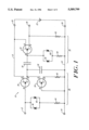
- FIG. 1 illustrates a presently preferred embodiment of the invention.
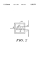
- FIG. 2 illustrates an alternative form of JFET transistor having an asymmetric source and drain configuration.
- the presently preferred embodiment of this invention is a preamplifier designated generally at 10, which is provided with input terminals 12 and 14 for connection to an electroacoustic transducer, for example an electret based condenser microphone used in hearing aids.
- an electroacoustic transducer for example an electret based condenser microphone used in hearing aids.
- Such transducers are characterized by a high output impedance and generally by some acoustic source noise, for example noise caused by acoustic resistive losses.
- One of these terminals is connected to the ground rail 16 of the circuit.
- An upper power supply rail 18 is connected to a terminal 20, and a dc source 22 which may be as low as 0.9 volt, for example, is connected between the terminal 20 and a terminal 24 which is connected to the rail 16.
- the output signal appears between the terminal 24 and a terminal 26.
- the circuit generally comprises a first stage 28 having a first JFET 30 connected in follower mode, and a second stage 32 having a second JFET 34 also connected in follower mode.
- the stages are interconnected by a shunt capacitor 36 and a coupling capacitor 38 the functions of which are respectively described below.
- the source, gate and drain terminals of the respective field effect transistors are correspondingly labeled "S,” “G” and “D,” respectively.
- the gate bias impedance circuit for the JFET 30 comprise a pair of parallel connected diodes 40 and 42 of opposite polarity and a resistor 44 connected in series therewith.
- the diodes act as resistors whose value is hundreds of giga-ohms.
- the gate bias impedance circuit for the JFET 34 comprises a pair of parallel connected diodes 46 and 48 of opposite polarity and a resistor 50 in series therewith.
- the load impedance of the circuit connected between the source of the JFET 34 and the ground rail 16 comprises a resistor 52.
- a resistor may be similarly connected between the source of the JFET 30 and ground, it is preferred to provide a third JFET 54 having its gate connected to ground and having its source connected through a resistor 56 to ground. Alternatively, its source may be connected directly to ground. As so connected the JFET 54 acts as a current source.
- a characteristic of the present invention is that the first stage or input JFET 30 is very much smaller in size than the output or second stage JFET 34.
- the size of a conventional transistor such as the 2N4338 manufactured by Siliconix, National Semiconductor, and others.
- the JFET 30 is less than half and preferably less than one-third the size of the conventional 2N4338, and the JFET 34 is on the order of two or more times the size of the conventional 2N4338 transistor.
- the ratio of sizes of the two JFETS is preferably six to one, and may be much greater in some cases.
- the size of the JFET 54 is typically smaller than that of the JFET 30.
- the pinch off voltage for the JFET 54 is equal to or lower than that for the JFET 30.
- the JFET 54 operates as the load by acting substantially as a current source, and limits the current to approximately one microampere. Because of the small size of the JFET 30 and the low current of the JFET 54, the output impedance of the first stage 28 is much higher than that found in conventional JFET circuits connected in follower mode, and the transconductance of the JFET 30 is lower.
- the capacitor 36 in shunt with the output impedance of the first stage, acts to roll off the higher frequencies.
- the capacitor 38 couples the signal to the gate of the JFET 34, and may be on the order of 50 pfd, but notwithstanding its small size it does not attenuate the low audio frequencies because the JFET 34 has a very high input impedance.
- the JFET 34 is larger than a normal transistor used in such circuits, so that the output impedance is low without excessive current draw.
- the size of the diodes employed in the circuit is conveniently compared with that of a conventional 1N4148 small signal diode manufactured by National Semiconductor, taken as a standard for reference.
- the diodes 40 and 42 are much smaller than the reference diode, for example one-tenth the size thereof, so as to minimize shunt capacitance and maximize shunt resistance.
- the value of the shunt capacitor 36 is chosen such that the combination of the first stage output impedance and the capacitor 36 forms an RC roll off at frequencies above a characteristic frequency f o .
- the latter frequency is chosen to coincide approximately with the incipient peaking of the acoustic circuit, resulting in a substantially flat overall response within the desired frequency pass band and an attenuation of the peak. Above the pass band, it results in an additional 6 dB per octave roll off beyond that which normally occurs from acoustic elements. The overall result is therefore a decrease in the total acoustic noise contribution of the source transducer.
- RC roll off has the further advantage that it can attenuate ultrasonic acoustic pickup and reduce the tendency for overload.
- circuits herein described may be constructed, in which the condenser 36 is replaced by an impedance network specifically designed to produce band acceptance, band rejection, high pass or low pass filtering, as dictated by the particular frequency shaping requirements of the application.
- impedance network specifically designed to produce band acceptance, band rejection, high pass or low pass filtering, as dictated by the particular frequency shaping requirements of the application.
- such networks may include inductive and resistive impedances or inductive, resistive and capacitive impedances.
- a further improvement may be made in the above-described circuit by employing a JFET 30 of asymmetric source and drain configuration, shown in FIG. 2 as a JFET 30A.
- the drain has fewer "fingers” 58 than the "fingers" 60 of the source, with the result that when compared to a symmetric geometry the device will have a lower gate-to-drain capacitance and hence a lower power supply feedthrough.
Landscapes
- Engineering & Computer Science (AREA)
- Multimedia (AREA)
- Power Engineering (AREA)
- Amplifiers (AREA)
Abstract
Description
Claims (12)
Priority Applications (6)
| Application Number | Priority Date | Filing Date | Title |
|---|---|---|---|
| US08/447,349 US5589799A (en) | 1994-09-29 | 1995-05-23 | Low noise amplifier for microphone |
| PCT/US1995/011838 WO1996010291A1 (en) | 1994-09-29 | 1995-09-19 | Low noise amplifier for microphone |
| DE69506727T DE69506727T2 (en) | 1994-09-29 | 1995-09-19 | SILENT AMPLIFIERS FOR MICROPHONES |
| AU35913/95A AU3591395A (en) | 1994-09-29 | 1995-09-19 | Low noise amplifier for microphone |
| DK95933142T DK0783795T3 (en) | 1994-09-29 | 1995-09-19 | Quiet amplifier for microphone |
| EP95933142A EP0783795B1 (en) | 1994-09-29 | 1995-09-19 | Low noise amplifier for microphone |
Applications Claiming Priority (2)
| Application Number | Priority Date | Filing Date | Title |
|---|---|---|---|
| US31469494A | 1994-09-29 | 1994-09-29 | |
| US08/447,349 US5589799A (en) | 1994-09-29 | 1995-05-23 | Low noise amplifier for microphone |
Related Parent Applications (1)
| Application Number | Title | Priority Date | Filing Date |
|---|---|---|---|
| US31469494A Continuation | 1994-09-29 | 1994-09-29 |
Publications (1)
| Publication Number | Publication Date |
|---|---|
| US5589799A true US5589799A (en) | 1996-12-31 |
Family
ID=26979502
Family Applications (1)
| Application Number | Title | Priority Date | Filing Date |
|---|---|---|---|
| US08/447,349 Expired - Fee Related US5589799A (en) | 1994-09-29 | 1995-05-23 | Low noise amplifier for microphone |
Country Status (6)
| Country | Link |
|---|---|
| US (1) | US5589799A (en) |
| EP (1) | EP0783795B1 (en) |
| AU (1) | AU3591395A (en) |
| DE (1) | DE69506727T2 (en) |
| DK (1) | DK0783795T3 (en) |
| WO (1) | WO1996010291A1 (en) |
Cited By (28)
| Publication number | Priority date | Publication date | Assignee | Title |
|---|---|---|---|---|
| EP0880225A2 (en) * | 1997-05-23 | 1998-11-25 | Tibbetts Industries, Inc. | Amplifier with reduced input capacitance |
| EP0969695A1 (en) * | 1998-07-02 | 2000-01-05 | Microtronic Nederland B.V. | System consisting of a microphone and a preamplifier |
| WO2000041432A2 (en) * | 1999-01-07 | 2000-07-13 | Sarnoff Corporation | Hearing aid with large diaphragm microphone element including a printed circuit board |
| US6147556A (en) * | 1997-11-04 | 2000-11-14 | Nec Corporation | Solid-state image sensor |
| US6392491B1 (en) * | 1999-02-25 | 2002-05-21 | Fujitsu Limited | High-frequency amplifier and amplification element |
| US20020125949A1 (en) * | 2001-03-09 | 2002-09-12 | Stenberg Lars J. | Electret condensor microphone preamplifier that is insensitive to leakage currents at the input |
| WO2002078177A1 (en) * | 2001-03-26 | 2002-10-03 | Georg Neumann Gmbh | Amplifying circuit |
| US20030076967A1 (en) * | 2001-09-24 | 2003-04-24 | Andres Hohendahl | Microphone preamplifier |
| US6577187B1 (en) | 2000-06-15 | 2003-06-10 | Upstate Audio | Powered transducer preamplifier with DC level shifting circuit |
| US20030193354A1 (en) * | 2002-04-15 | 2003-10-16 | Potter Robert C. | Switched microphone buffer |
| US20030194100A1 (en) * | 2002-04-15 | 2003-10-16 | Boor Steven E. | Microphone input buffer biasing circuit |
| US20030202669A1 (en) * | 2002-04-24 | 2003-10-30 | Boor Steven E. | Electret microphone buffer circuit with significantly enhanced power supply rejection |
| US20040085137A1 (en) * | 2002-08-27 | 2004-05-06 | Furst Claus Erdmann | Preamplifier for two terminal electret condenser microphones |
| US7003127B1 (en) | 1999-01-07 | 2006-02-21 | Sarnoff Corporation | Hearing aid with large diaphragm microphone element including a printed circuit board |
| US20060109998A1 (en) * | 2004-11-24 | 2006-05-25 | Mwm Acoustics, Llc (An Indiana Limited Liability Company) | System and method for RF immunity of electret condenser microphone |
| US7292700B1 (en) | 1999-04-13 | 2007-11-06 | Sonion Nederland B.V. | Microphone for a hearing aid |
| US20070297623A1 (en) * | 2006-06-26 | 2007-12-27 | Nokia Corporation | Apparatus and method to provide advanced microphone bias |
| US20080258816A1 (en) * | 2006-11-21 | 2008-10-23 | Industrial Technology Research Institute | Low frequency analog circuit and design method thereof |
| US20090268926A1 (en) * | 2008-03-17 | 2009-10-29 | Nec Electronics Corporation | Semiconductor integrated circuit and condenser microphone |
| EP2461605A1 (en) * | 2010-12-06 | 2012-06-06 | Research In Motion Limited | Differential microphone circuit |
| US20140097906A1 (en) * | 2012-10-02 | 2014-04-10 | Knowles Electronics, Llc | Single Stage Buffer With Filter |
| US8750537B2 (en) | 2010-12-06 | 2014-06-10 | Blackberry Limited | Differential microphone circuit |
| US8831263B2 (en) | 2003-10-31 | 2014-09-09 | Bose Corporation | Porting |
| US20150070803A1 (en) * | 2013-09-12 | 2015-03-12 | Qualcomm Incorporated | Electro-static discharge protection for integrated circuits |
| WO2015097681A3 (en) * | 2013-12-25 | 2015-11-12 | Wizedsp Ltd | Systems and methods for using electrostatic microphone |
| WO2016185426A1 (en) * | 2015-05-20 | 2016-11-24 | Wizedsp Ltd. | An ultra-low-power and low-noise amplifier |
| CN107231140A (en) * | 2017-06-07 | 2017-10-03 | 广州致远电子有限公司 | A kind of impedance transformer network circuit structure |
| US10356507B1 (en) * | 2009-10-09 | 2019-07-16 | Cloud Microphones, LLC. | Phantom powered JFET circuit for audio application |
Families Citing this family (2)
| Publication number | Priority date | Publication date | Assignee | Title |
|---|---|---|---|---|
| US6353344B1 (en) | 2000-05-22 | 2002-03-05 | Microtronic Us, Inc. | High impedance bias circuit |
| US7149317B2 (en) | 2002-04-18 | 2006-12-12 | Sonionmicrotronic Nederland B.V. | CMOS high impedance circuit |
Citations (11)
| Publication number | Priority date | Publication date | Assignee | Title |
|---|---|---|---|---|
| US3512100A (en) * | 1968-07-03 | 1970-05-12 | Intern Research Products Inc | Audio frequency amplification circuit |
| US3801933A (en) * | 1972-04-17 | 1974-04-02 | Rca Ltd | Low noise detector amplifier |
| US3927383A (en) * | 1972-04-21 | 1975-12-16 | Rca Corp | Low noise wide band transducer system |
| US3993869A (en) * | 1972-03-02 | 1976-11-23 | Sony Corporation | Amplifying circuit for use with a high impedance source transducer |
| US4151480A (en) * | 1976-12-30 | 1979-04-24 | Industrial Research Products, Inc. | FET Amplifier with protective circuit |
| US5017887A (en) * | 1988-12-09 | 1991-05-21 | U.S. Philips Corporation | High frequency IC power amplifier |
| US5027080A (en) * | 1989-07-06 | 1991-06-25 | Sumitomo Electric Industries, Ltd. | Source follower light reception circuit |
| US5083095A (en) * | 1990-08-22 | 1992-01-21 | Knowles Electronics, Inc. | Plural source follower amplifier |
| US5097224A (en) * | 1991-04-11 | 1992-03-17 | Telex Communications, Inc. | Self-biasing, low noise amplifier of extended dynamic range |
| US5214709A (en) * | 1990-07-13 | 1993-05-25 | Viennatone Gesellschaft M.B.H. | Hearing aid for persons with an impaired hearing faculty |
| US5337011A (en) * | 1992-12-14 | 1994-08-09 | Knowles Electronics, Inc. | Pre-amplifier |
-
1995
- 1995-05-23 US US08/447,349 patent/US5589799A/en not_active Expired - Fee Related
- 1995-09-19 WO PCT/US1995/011838 patent/WO1996010291A1/en active IP Right Grant
- 1995-09-19 AU AU35913/95A patent/AU3591395A/en not_active Abandoned
- 1995-09-19 EP EP95933142A patent/EP0783795B1/en not_active Expired - Lifetime
- 1995-09-19 DE DE69506727T patent/DE69506727T2/en not_active Expired - Fee Related
- 1995-09-19 DK DK95933142T patent/DK0783795T3/en active
Patent Citations (11)
| Publication number | Priority date | Publication date | Assignee | Title |
|---|---|---|---|---|
| US3512100A (en) * | 1968-07-03 | 1970-05-12 | Intern Research Products Inc | Audio frequency amplification circuit |
| US3993869A (en) * | 1972-03-02 | 1976-11-23 | Sony Corporation | Amplifying circuit for use with a high impedance source transducer |
| US3801933A (en) * | 1972-04-17 | 1974-04-02 | Rca Ltd | Low noise detector amplifier |
| US3927383A (en) * | 1972-04-21 | 1975-12-16 | Rca Corp | Low noise wide band transducer system |
| US4151480A (en) * | 1976-12-30 | 1979-04-24 | Industrial Research Products, Inc. | FET Amplifier with protective circuit |
| US5017887A (en) * | 1988-12-09 | 1991-05-21 | U.S. Philips Corporation | High frequency IC power amplifier |
| US5027080A (en) * | 1989-07-06 | 1991-06-25 | Sumitomo Electric Industries, Ltd. | Source follower light reception circuit |
| US5214709A (en) * | 1990-07-13 | 1993-05-25 | Viennatone Gesellschaft M.B.H. | Hearing aid for persons with an impaired hearing faculty |
| US5083095A (en) * | 1990-08-22 | 1992-01-21 | Knowles Electronics, Inc. | Plural source follower amplifier |
| US5097224A (en) * | 1991-04-11 | 1992-03-17 | Telex Communications, Inc. | Self-biasing, low noise amplifier of extended dynamic range |
| US5337011A (en) * | 1992-12-14 | 1994-08-09 | Knowles Electronics, Inc. | Pre-amplifier |
Non-Patent Citations (4)
| Title |
|---|
| Edwin S. Oxner, FET Technology and Application, An Introduction , pp. 98, 99, published by Marcel Dekker, Inc., New York, 1989. * |
| Edwin S. Oxner, FET Technology and Application, An Introduction, pp. 98, 99, published by Marcel Dekker, Inc., New York, 1989. |
| Instruments and Experimental Techniques, vol. 16, No. 3, May Jun. 1973, pp. 837 838, article A Thermally Durable Preamplifier by I. N. Poznyak et al. * |
| Instruments and Experimental Techniques, vol. 16, No. 3, May-Jun. 1973, pp. 837-838, article "A Thermally Durable Preamplifier" by I. N. Poznyak et al. |
Cited By (58)
| Publication number | Priority date | Publication date | Assignee | Title |
|---|---|---|---|---|
| US6023194A (en) * | 1997-05-23 | 2000-02-08 | Tibbetts Industries, Inc. | Amplifier with reduced input capacitance |
| EP0880225A3 (en) * | 1997-05-23 | 2001-01-24 | Tibbetts Industries, Inc. | Amplifier with reduced input capacitance |
| EP0880225A2 (en) * | 1997-05-23 | 1998-11-25 | Tibbetts Industries, Inc. | Amplifier with reduced input capacitance |
| US6147556A (en) * | 1997-11-04 | 2000-11-14 | Nec Corporation | Solid-state image sensor |
| EP0969695A1 (en) * | 1998-07-02 | 2000-01-05 | Microtronic Nederland B.V. | System consisting of a microphone and a preamplifier |
| US20060177083A1 (en) * | 1999-01-07 | 2006-08-10 | Sjursen Walter P | Hearing aid with large diaphragm microphone element including a printed circuit board |
| WO2000041432A2 (en) * | 1999-01-07 | 2000-07-13 | Sarnoff Corporation | Hearing aid with large diaphragm microphone element including a printed circuit board |
| WO2000041432A3 (en) * | 1999-01-07 | 2000-11-30 | Sarnoff Corp | Hearing aid with large diaphragm microphone element including a printed circuit board |
| US7003127B1 (en) | 1999-01-07 | 2006-02-21 | Sarnoff Corporation | Hearing aid with large diaphragm microphone element including a printed circuit board |
| US7221768B2 (en) | 1999-01-07 | 2007-05-22 | Sarnoff Corporation | Hearing aid with large diaphragm microphone element including a printed circuit board |
| US20070121967A1 (en) * | 1999-01-07 | 2007-05-31 | Sjursen Walter P | Hearing aid with large diaphragm microphone element including a printed circuit board |
| US6392491B1 (en) * | 1999-02-25 | 2002-05-21 | Fujitsu Limited | High-frequency amplifier and amplification element |
| US8824713B2 (en) | 1999-04-13 | 2014-09-02 | Sonion Nederland B.V. | Microphone for a hearing aid |
| US8369552B2 (en) | 1999-04-13 | 2013-02-05 | Sonion Nederland B.V. | Microphone for a hearing aid |
| US20070258610A1 (en) * | 1999-04-13 | 2007-11-08 | Sonionmicrotronic Nederland B.V. | Microphone for a hearing aid |
| US7292700B1 (en) | 1999-04-13 | 2007-11-06 | Sonion Nederland B.V. | Microphone for a hearing aid |
| US6577187B1 (en) | 2000-06-15 | 2003-06-10 | Upstate Audio | Powered transducer preamplifier with DC level shifting circuit |
| US20020125949A1 (en) * | 2001-03-09 | 2002-09-12 | Stenberg Lars J. | Electret condensor microphone preamplifier that is insensitive to leakage currents at the input |
| US7110560B2 (en) * | 2001-03-09 | 2006-09-19 | Sonion A/S | Electret condensor microphone preamplifier that is insensitive to leakage currents at the input |
| US20040131210A1 (en) * | 2001-03-26 | 2004-07-08 | Otmar Kern | Amplifying circuit |
| US6812788B2 (en) | 2001-03-26 | 2004-11-02 | Georg Neumann Gmbh | Amplifying circuit |
| WO2002078177A1 (en) * | 2001-03-26 | 2002-10-03 | Georg Neumann Gmbh | Amplifying circuit |
| US20030076967A1 (en) * | 2001-09-24 | 2003-04-24 | Andres Hohendahl | Microphone preamplifier |
| US7072478B2 (en) * | 2001-09-24 | 2006-07-04 | Taylor Hohendahl Engineering Llp | Microphone preamplifier |
| EP1355417A1 (en) * | 2002-04-15 | 2003-10-22 | Knowles Electronics, LLC | Microphone input buffer biasing circuit |
| US20030194100A1 (en) * | 2002-04-15 | 2003-10-16 | Boor Steven E. | Microphone input buffer biasing circuit |
| US20030193354A1 (en) * | 2002-04-15 | 2003-10-16 | Potter Robert C. | Switched microphone buffer |
| US7092538B2 (en) | 2002-04-15 | 2006-08-15 | Knowles Electronics, Llc | Switched microphone buffer |
| US7221766B2 (en) | 2002-04-15 | 2007-05-22 | Knowles Electronics, Llc | Microphone input buffer biasing circuit |
| US20030202669A1 (en) * | 2002-04-24 | 2003-10-30 | Boor Steven E. | Electret microphone buffer circuit with significantly enhanced power supply rejection |
| EP1359664A1 (en) * | 2002-04-24 | 2003-11-05 | Knowles Electronics, LLC | Electret microphone buffer circuit with significantly enhanced power supply rejection |
| US7688987B2 (en) | 2002-04-24 | 2010-03-30 | Knowles Electronics, Llc | Electret microphone buffer circuit with significantly enhanced power supply rejection |
| US20040085137A1 (en) * | 2002-08-27 | 2004-05-06 | Furst Claus Erdmann | Preamplifier for two terminal electret condenser microphones |
| US6888408B2 (en) * | 2002-08-27 | 2005-05-03 | Sonion Tech A/S | Preamplifier for two terminal electret condenser microphones |
| US8831263B2 (en) | 2003-10-31 | 2014-09-09 | Bose Corporation | Porting |
| US20060109998A1 (en) * | 2004-11-24 | 2006-05-25 | Mwm Acoustics, Llc (An Indiana Limited Liability Company) | System and method for RF immunity of electret condenser microphone |
| US7787643B2 (en) * | 2004-11-24 | 2010-08-31 | Mwm Acoustics, Llc | System and method for RF immunity of electret condenser microphone |
| US20070297623A1 (en) * | 2006-06-26 | 2007-12-27 | Nokia Corporation | Apparatus and method to provide advanced microphone bias |
| US7978863B2 (en) | 2006-06-26 | 2011-07-12 | Nokia Corporation | Apparatus and method to provide advanced microphone bias |
| US20080258816A1 (en) * | 2006-11-21 | 2008-10-23 | Industrial Technology Research Institute | Low frequency analog circuit and design method thereof |
| US7719358B2 (en) | 2006-11-21 | 2010-05-18 | Industrial Technology Research Institute | Low frequency analog circuit and design method thereof |
| US8111844B2 (en) * | 2008-03-17 | 2012-02-07 | Renesas Electronics Corporation | Semiconductor integrated circuit and condenser microphone |
| US20090268926A1 (en) * | 2008-03-17 | 2009-10-29 | Nec Electronics Corporation | Semiconductor integrated circuit and condenser microphone |
| US10721552B1 (en) * | 2009-10-09 | 2020-07-21 | Cloud Microphones, Llc | Phantom powered FET circuit for audio application |
| US10356507B1 (en) * | 2009-10-09 | 2019-07-16 | Cloud Microphones, LLC. | Phantom powered JFET circuit for audio application |
| US8750537B2 (en) | 2010-12-06 | 2014-06-10 | Blackberry Limited | Differential microphone circuit |
| EP2461605A1 (en) * | 2010-12-06 | 2012-06-06 | Research In Motion Limited | Differential microphone circuit |
| US9590571B2 (en) * | 2012-10-02 | 2017-03-07 | Knowles Electronics, Llc | Single stage buffer with filter |
| US20140097906A1 (en) * | 2012-10-02 | 2014-04-10 | Knowles Electronics, Llc | Single Stage Buffer With Filter |
| US9608437B2 (en) * | 2013-09-12 | 2017-03-28 | Qualcomm Incorporated | Electro-static discharge protection for integrated circuits |
| US20150070803A1 (en) * | 2013-09-12 | 2015-03-12 | Qualcomm Incorporated | Electro-static discharge protection for integrated circuits |
| US20160337751A1 (en) * | 2013-12-25 | 2016-11-17 | Wizedsp Ltd. | Systems and methods for using electrostatic microphone |
| CN105981405A (en) * | 2013-12-25 | 2016-09-28 | 怀斯迪斯匹有限公司 | Systems and methods for using electrostatic microphone |
| US9961440B2 (en) * | 2013-12-25 | 2018-05-01 | Wizedsp Ltd. | Systems and methods for using electrostatic microphone |
| WO2015097681A3 (en) * | 2013-12-25 | 2015-11-12 | Wizedsp Ltd | Systems and methods for using electrostatic microphone |
| WO2016185426A1 (en) * | 2015-05-20 | 2016-11-24 | Wizedsp Ltd. | An ultra-low-power and low-noise amplifier |
| CN107231140A (en) * | 2017-06-07 | 2017-10-03 | 广州致远电子有限公司 | A kind of impedance transformer network circuit structure |
| CN107231140B (en) * | 2017-06-07 | 2020-12-04 | 广州致远电子有限公司 | Impedance transformation network circuit structure |
Also Published As
| Publication number | Publication date |
|---|---|
| DE69506727D1 (en) | 1999-01-28 |
| EP0783795A1 (en) | 1997-07-16 |
| WO1996010291A1 (en) | 1996-04-04 |
| DK0783795T3 (en) | 1999-08-23 |
| DE69506727T2 (en) | 1999-06-10 |
| EP0783795B1 (en) | 1998-12-16 |
| AU3591395A (en) | 1996-04-19 |
Similar Documents
| Publication | Publication Date | Title |
|---|---|---|
| US5589799A (en) | Low noise amplifier for microphone | |
| US5083095A (en) | Plural source follower amplifier | |
| US6822507B2 (en) | Adaptive speech filter | |
| EP0664605B1 (en) | Amplifier device | |
| US8890615B2 (en) | Buffering apparatus and method | |
| JPS6134749Y2 (en) | ||
| US20090021293A1 (en) | Low-Power Integrated-Circuit Signal Processor With Wide Dynamic Range | |
| JPH08505753A (en) | Device and method for frequency compensating operational amplifiers | |
| US6023194A (en) | Amplifier with reduced input capacitance | |
| US5327027A (en) | Circuit for multiplying the value of a capacitor | |
| US4521741A (en) | Impedance transformer circuit | |
| US7688987B2 (en) | Electret microphone buffer circuit with significantly enhanced power supply rejection | |
| US5459792A (en) | Audio input circuit for voice recognition | |
| JP3148348B2 (en) | Pre-attenuator for displacement proportional transducer | |
| US5745587A (en) | Hearing aid amplifier circuitry | |
| JPH10150328A (en) | Electronic circuit converting differential input voltage into single end output voltage | |
| US20230327614A1 (en) | Super source follower | |
| CN114928335A (en) | Low-noise audio amplifier and equipment | |
| CN210629837U (en) | Audio control circuit and equipment | |
| US3014995A (en) | Transistor hearing aid | |
| EP0362219B1 (en) | Asymmetrical dual input amplifier | |
| JP3057397B2 (en) | Displacement proportional transducer | |
| US3683290A (en) | Automatic volume control through preamplifier supply voltages | |
| JP2515821B2 (en) | Control amplifier | |
| KR100188108B1 (en) | Noise decreasing method of filter combining amplifier |
Legal Events
| Date | Code | Title | Description |
|---|---|---|---|
| AS | Assignment |
Owner name: TIBBETTS INDUSTRIES, INC., MAINE Free format text: ASSIGNMENT OF ASSIGNORS INTEREST;ASSIGNORS:MADAFFARI, PETER L.;COLLINS, JAMES S.;REEL/FRAME:007493/0048 Effective date: 19950522 |
|
| FEPP | Fee payment procedure |
Free format text: PAYOR NUMBER ASSIGNED (ORIGINAL EVENT CODE: ASPN); ENTITY STATUS OF PATENT OWNER: SMALL ENTITY |
|
| CC | Certificate of correction | ||
| REMI | Maintenance fee reminder mailed | ||
| FEPP | Fee payment procedure |
Free format text: PETITION RELATED TO MAINTENANCE FEES GRANTED (ORIGINAL EVENT CODE: PMFG); ENTITY STATUS OF PATENT OWNER: SMALL ENTITY |
|
| FPAY | Fee payment |
Year of fee payment: 4 |
|
| SULP | Surcharge for late payment | ||
| FP | Lapsed due to failure to pay maintenance fee |
Effective date: 20001231 |
|
| PRDP | Patent reinstated due to the acceptance of a late maintenance fee |
Effective date: 20010223 |
|
| FPAY | Fee payment |
Year of fee payment: 8 |
|
| REMI | Maintenance fee reminder mailed | ||
| LAPS | Lapse for failure to pay maintenance fees | ||
| STCH | Information on status: patent discontinuation |
Free format text: PATENT EXPIRED DUE TO NONPAYMENT OF MAINTENANCE FEES UNDER 37 CFR 1.362 |
|
| FP | Lapsed due to failure to pay maintenance fee |
Effective date: 20081231 |