US7221766B2 - Microphone input buffer biasing circuit - Google Patents
Microphone input buffer biasing circuit Download PDFInfo
- Publication number
- US7221766B2 US7221766B2 US10/411,556 US41155603A US7221766B2 US 7221766 B2 US7221766 B2 US 7221766B2 US 41155603 A US41155603 A US 41155603A US 7221766 B2 US7221766 B2 US 7221766B2
- Authority
- US
- United States
- Prior art keywords
- input
- transistor
- circuit
- operably connected
- biasing
- Prior art date
- Legal status (The legal status is an assumption and is not a legal conclusion. Google has not performed a legal analysis and makes no representation as to the accuracy of the status listed.)
- Expired - Fee Related, expires
Links
- 239000000872 buffer Substances 0.000 title claims description 45
- 230000003071 parasitic effect Effects 0.000 claims description 11
- 238000002955 isolation Methods 0.000 claims 1
- 230000008901 benefit Effects 0.000 description 3
- 238000004519 manufacturing process Methods 0.000 description 3
- 238000000034 method Methods 0.000 description 3
- 230000009467 reduction Effects 0.000 description 3
- 230000001052 transient effect Effects 0.000 description 3
- 230000002411 adverse Effects 0.000 description 2
- 230000003139 buffering effect Effects 0.000 description 2
- 230000015556 catabolic process Effects 0.000 description 2
- 238000006731 degradation reaction Methods 0.000 description 2
- 230000007613 environmental effect Effects 0.000 description 2
- 238000012986 modification Methods 0.000 description 2
- 230000004048 modification Effects 0.000 description 2
- 238000012545 processing Methods 0.000 description 2
- 230000006978 adaptation Effects 0.000 description 1
- 238000005513 bias potential Methods 0.000 description 1
- 238000013461 design Methods 0.000 description 1
- 238000011161 development Methods 0.000 description 1
- 230000006870 function Effects 0.000 description 1
- 238000010348 incorporation Methods 0.000 description 1
- 238000011084 recovery Methods 0.000 description 1
- 238000011160 research Methods 0.000 description 1
- 230000035945 sensitivity Effects 0.000 description 1
- 230000005236 sound signal Effects 0.000 description 1
Images


Classifications
-
- H—ELECTRICITY
- H03—ELECTRONIC CIRCUITRY
- H03F—AMPLIFIERS
- H03F1/00—Details of amplifiers with only discharge tubes, only semiconductor devices or only unspecified devices as amplifying elements
- H03F1/30—Modifications of amplifiers to reduce influence of variations of temperature or supply voltage or other physical parameters
- H03F1/305—Modifications of amplifiers to reduce influence of variations of temperature or supply voltage or other physical parameters in case of switching on or off of a power supply
-
- H—ELECTRICITY
- H03—ELECTRONIC CIRCUITRY
- H03F—AMPLIFIERS
- H03F1/00—Details of amplifiers with only discharge tubes, only semiconductor devices or only unspecified devices as amplifying elements
- H03F1/30—Modifications of amplifiers to reduce influence of variations of temperature or supply voltage or other physical parameters
- H03F1/301—Modifications of amplifiers to reduce influence of variations of temperature or supply voltage or other physical parameters in MOSFET amplifiers
-
- H—ELECTRICITY
- H03—ELECTRONIC CIRCUITRY
- H03F—AMPLIFIERS
- H03F1/00—Details of amplifiers with only discharge tubes, only semiconductor devices or only unspecified devices as amplifying elements
- H03F1/52—Circuit arrangements for protecting such amplifiers
- H03F1/523—Circuit arrangements for protecting such amplifiers for amplifiers using field-effect devices
-
- H—ELECTRICITY
- H03—ELECTRONIC CIRCUITRY
- H03F—AMPLIFIERS
- H03F3/00—Amplifiers with only discharge tubes or only semiconductor devices as amplifying elements
- H03F3/181—Low-frequency amplifiers, e.g. audio preamplifiers
- H03F3/183—Low-frequency amplifiers, e.g. audio preamplifiers with semiconductor devices only
- H03F3/185—Low-frequency amplifiers, e.g. audio preamplifiers with semiconductor devices only with field-effect devices
-
- H—ELECTRICITY
- H03—ELECTRONIC CIRCUITRY
- H03F—AMPLIFIERS
- H03F2200/00—Indexing scheme relating to amplifiers
- H03F2200/03—Indexing scheme relating to amplifiers the amplifier being designed for audio applications
-
- H—ELECTRICITY
- H03—ELECTRONIC CIRCUITRY
- H03F—AMPLIFIERS
- H03F2200/00—Indexing scheme relating to amplifiers
- H03F2200/18—Indexing scheme relating to amplifiers the bias of the gate of a FET being controlled by a control signal
Definitions
- the present invention relates to microphones. More specifically, the present invention is directed to a biasing circuit utilized in an input buffer for a microphone.
- Hearing aid performance continues to be enhanced by technological advances in audio signal processing capabilities, e.g. primarily via digital signal processing, environmental adaptation, programmability, and noise cancellation techniques. As part of these on-going advancement efforts, hearing aid manufacturers often request performance improvements from suppliers of microphone transducers.
- the anti-parallel diode biasing circuitry coupled to the signal input of the microphone will effectively limit the transducer output to the turn-on voltage, V on , of the diodes, e.g., +/ ⁇ 0.3V, relative to the zero-bias potential.
- diode biasing has been a major factor leading to significantly improved microphone noise performance, it has been noted that diode biasing also results in undesirable audible artifacts and performance degradation in directional hearing aids. Frequently, such performance degradation occurs under loud acoustic transient conditions, i.e., when the signal level voltage from the transducer would normally exceed V on .
- an alternative input biasing configuration is desirable to adapt the microphone buffer to accommodate environmental conditions for alleviating these audible artifacts without compromising overall noise performance in the transducer.
- One embodiment of the present invention is directed to an input buffer biasing circuit for a microphone assembly.
- the circuit comprises an input transistor being operably connected between an input and an output.
- a biasing circuit is operably connected to the input and the input transistor.
- a resistor is operably connected to the input transistor and the output. The resistor and the input transistor cooperate to provide a buffered version of a voltage signal received at the input to the output.
- Another object of the present invention is to limit the impedance reduction and the amount of current flow through an input biasing circuit of an input buffer for an assisted-listening system and/or device, e.g., hearing aid.
- Yet another object of the present invention is to provide the ability to completely integrate the current limiting circuitry of an input buffer onto an integrated circuit.
- Another further object of the present invention is to reduce manufacturing costs, improve reliability, and improve hearing aid performance by reducing and/or eliminating the need to use large, external, discrete, components in a microphone input buffer for the hearing aid.
- FIG. 1 a depicts a prior art input buffer circuit for a microphone incorporating a commonly known input biasing technique utilizing anti-parallel input bias diodes to attain ultra-low noise circuit performance;
- FIG. 1 b depicts another prior art input buffer circuit for a microphone utilizing an externally connected Giga-ohm valued resistor to introduce a lower limit to the impedance of the input biasing circuitry;
- FIG. 1 c depicts an input buffer circuit for a microphone in accordance with one embodiment of the present invention
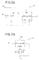
- FIG. 2 a depicts one embodiment of a biasing circuit of the present invention
- FIG. 2 b depicts another embodiment of a biasing circuit of the present invention
- FIG. 3 a depicts a partial schematic drawing of one embodiment of the input buffer biasing circuit of the present invention utilizing the biasing circuit shown in FIG. 2 a;
- FIG. 3 b depicts a partial schematic drawing of another embodiment of the input buffer biasing circuit of the present invention utilizing the biasing circuit shown in FIG. 2 b;
- FIG. 4 is a graph depicting the square law characteristic of the buffer input transistor 16 in FIG. 1 c ;
- FIG. 5 is a graphical comparison of electrical characteristics of various input biasing circuits for a microphone.
- FIG. 1 a One known embodiment of an input buffer circuit for a microphone commonly utilized to obtain ultra-low noise circuit performance is shown in FIG. 1 a .
- the circuit utilizes anti-parallel input bias diodes for input biasing the input transistor of the buffer circuit.
- Another commonly used technique to input bias the input transistor incorporates externally connected Giga-ohm resistor(s) to introduce a lower limit to the impedance of the input biasing circuit, such as shown in FIG. 1 b . See also, U.S. Pat. Nos. 5,097,224 and 5,589,799.
- the design of these input buffers require costly manufacturing processes that may adversely affect the performance and reliability of the input buffer circuit.
- FIG. 1 c An input buffer biasing circuit 10 of the present invention is illustrated in FIG. 1 c .
- the circuit 10 includes a signal input terminal 12 operably connected to a signal output terminal 14 .
- the circuit 10 further includes an input transistor 16 operably connected to the input 12 and output 14 .
- a biasing circuit 18 is connected to the input 12 and the input transistor 16 .
- a resistor 20 connects the output terminal 14 and the input transistor 16 to ground.
- the biasing circuit 18 DC biases the gate terminal of the input transistor 16 .
- the input transistor 16 buffers the impedance between the high impedance of a transducer of an electret microphone (not shown) and the relatively lower impedance of a hearing aid circuit (not shown), e.g., amplifier, signal processor.
- the resistor 20 cooperates with the input transistor 16 , preferably Depletion NMOS, to provide the desired amount of voltage signal, e.g., received from a transducer, to the hearing aid circuit.
- FIG. 2 a depicts one embodiment of the biasing circuit 18 .
- a current limiter 22 is operably connected to a pair of diodes 24 , 26 .
- Each diode 24 , 26 is operably connected in series to the current limiting device 22 .
- the current limiting device 22 limits the amount of current flowing into and out of the biasing circuit 18 and through the diodes 24 , 26 . Without some means of limiting the current through the input biasing circuitry, increased current levels through the input biasing circuitry (resulting from an increase in the input signal voltage) will adversely affect the transient recovery characteristics of a completed microphone assembly, usually resulting in undesirable artificial acoustic sound artifacts.
- FIG. 3 a One embodiment of the current limiter 22 capable of being utilized with the biasing circuit 18 of the present invention is depicted in FIG. 3 a . Since each diode 24 , 26 conducts current in one direction only, a pair of transistors 28 , 30 are utilized for current limiting in each direction, i.e., during forward biasing of each respective diode.
- a buffering circuit 32 is operably connected to the input terminal 12 and the first and second transistors 28 , 30 to buffer the parasitic junction capacitance associated with isolating the P-well regions of the transistors.
- the first and second transistors 28 , 30 are Natural NMOS type devices and have a threshold voltage near 0 volts.
- the first and second transistors 28 , 30 perform the current limiting function of the biasing limiter circuit 18 .
- the buffer circuit 32 is comprised of a resistor 34 and three operably connected enhancement PMOS transistors 36 , 38 , 40 .
- FIG. 3 a also shows a pair of diodes 42 , 44 that are parasitic structures in the physical implementation of the current limiting circuitry.
- the capacitance associated with these parasitic diodes 42 , 44 are guarded-out by the PMOS buffer portion of the circuit.
- the square law characteristic of the input transistor 16 for the input buffer 10 of the present invention is shown in FIG. 4 .
- Current flowing through the input transistor 16 from its drain to its source, I DS is represented on the vertical axis of the graph.
- Voltage at the output terminal 14 is represented on the horizontal axis of the graph.
- the parabolic curves in the center portion of the graph represent the input transistor I DS characteristic for various input voltages, i.e., ⁇ 0.1, 0.0, and 0.1 volts.
- the intersection of the load line of the resistor 20 with the parabolic curve represents the drain-source current of the input transistor 16 and the voltage at the terminal output 14 .
- FIGS. 2 b and 3 b An alternative embodiment of the current limiter 22 capable of being utilized with the biasing circuit 18 of the present invention is depicted in FIGS. 2 b and 3 b .
- the current limiter 22 shown in FIG. 2 b is operably connected to a pair of anti-parallel diodes 24 , 26 .
- the current limiter 22 is a bi-directional current limiting circuit that symmetrically limits the amount of current flowing into and out of the biasing circuit 18 and through the anti-parallel diodes 24 , 26 .
- the first transistor 28 and second transistor 30 are operably connected between the input terminal 12 and the pair of anti-parallel diodes 24 , 26 of the biasing circuit 18 of FIG. 2 b .
- the buffering circuitry 32 includes a resistor 34 and three operably connected enhancement PMOS transistors 36 , 38 , 40 , and is operably connected to the input terminal 12 and the first and second transistors 28 , 30 to buffer the parasitic junction capacitance associated with isolating the P-well regions of the transistors.
- the present invention is structurally different and offers significant advantages over biasing circuits of prior art input buffers.
- Utilization of the input transistor 16 in cooperation with the Natural MOS transistors 28 , 30 allows for the incorporation of all the input buffer circuit components onto the same integrated circuit, which lowers manufacturing costs, improves reliability, and reduces the parasitic capacitances that degrade the overall microphone sensitivity.
- FIG. 5 The relationship between the output current, I out , and the input voltage, V in , for the biasing circuit 18 of the present invention and other known biasing circuits that incorporate anti-parallel diodes is shown in FIG. 5 .
- the solid line represents the preferred embodiment of the present invention.
- the remaining lines represent two commonly known art input bias circuits—the dotted line represents an input biasing circuit utilizing the anti-parallel diodes alone, e.g., FIG. 1 a , and the scored line represents an input buffer circuit utilizing the anti-parallel diodes in series with a discrete resistor(s) in the Giga-ohm range, e.g., FIG. 1 b . It is shown in FIG.
- the input buffer 10 of the present invention is functionally comparable to the input bias circuits used in FIG. 1 b , in that it effectively limits the current through the input bias circuitry to substantially the same level. It has been found that limiting the current flow through the input biasing circuitry to pico-Amp levels, and not limiting the impedance reduction of the input biasing circuitry per se, is the most critical factor in eliminating the acoustic artifact problem for large transient sound inputs. Moreover, the buffer circuit 10 of the present invention includes the additional economic, reliability, and performance advantages that result from the ability to completely integrate all circuitry onto the same IC.
Landscapes
- Engineering & Computer Science (AREA)
- Power Engineering (AREA)
- Multimedia (AREA)
- Amplifiers (AREA)
Abstract
Description
Claims (8)
Priority Applications (1)
| Application Number | Priority Date | Filing Date | Title |
|---|---|---|---|
| US10/411,556 US7221766B2 (en) | 2002-04-15 | 2003-04-10 | Microphone input buffer biasing circuit |
Applications Claiming Priority (2)
| Application Number | Priority Date | Filing Date | Title |
|---|---|---|---|
| US37254702P | 2002-04-15 | 2002-04-15 | |
| US10/411,556 US7221766B2 (en) | 2002-04-15 | 2003-04-10 | Microphone input buffer biasing circuit |
Publications (2)
| Publication Number | Publication Date |
|---|---|
| US20030194100A1 US20030194100A1 (en) | 2003-10-16 |
| US7221766B2 true US7221766B2 (en) | 2007-05-22 |
Family
ID=28675596
Family Applications (1)
| Application Number | Title | Priority Date | Filing Date |
|---|---|---|---|
| US10/411,556 Expired - Fee Related US7221766B2 (en) | 2002-04-15 | 2003-04-10 | Microphone input buffer biasing circuit |
Country Status (4)
| Country | Link |
|---|---|
| US (1) | US7221766B2 (en) |
| EP (1) | EP1355417B1 (en) |
| DE (1) | DE60309092T2 (en) |
| DK (1) | DK1355417T3 (en) |
Cited By (13)
| Publication number | Priority date | Publication date | Assignee | Title |
|---|---|---|---|---|
| CN101924525A (en) * | 2009-06-11 | 2010-12-22 | 音频专用集成电路公司 | High performance voice frequency amplifying circuit |
| US20110026739A1 (en) * | 2009-06-11 | 2011-02-03 | Audioasics A/S | High level capable audio amplification circuit |
| US20110029109A1 (en) * | 2009-06-11 | 2011-02-03 | Audioasics A/S | Audio signal controller |
| US9402131B2 (en) | 2013-10-30 | 2016-07-26 | Knowles Electronics, Llc | Push-pull microphone buffer |
| US9485594B2 (en) | 2014-08-06 | 2016-11-01 | Knowles Electronics, Llc | Connector arrangement in hearing instruments |
| US9590571B2 (en) | 2012-10-02 | 2017-03-07 | Knowles Electronics, Llc | Single stage buffer with filter |
| US9859879B2 (en) | 2015-09-11 | 2018-01-02 | Knowles Electronics, Llc | Method and apparatus to clip incoming signals in opposing directions when in an off state |
| EP3324646A1 (en) | 2016-11-18 | 2018-05-23 | Sonion Nederland B.V. | A circuit for providing a high and a low impedance and a system comprising the circuit |
| US10264361B2 (en) | 2016-11-18 | 2019-04-16 | Sonion Nederland B.V. | Transducer with a high sensitivity |
| US10327072B2 (en) | 2016-11-18 | 2019-06-18 | Sonion Nederland B.V. | Phase correcting system and a phase correctable transducer system |
| US10656006B2 (en) | 2016-11-18 | 2020-05-19 | Sonion Nederland B.V. | Sensing circuit comprising an amplifying circuit and an amplifying circuit |
| US11115744B2 (en) | 2018-04-02 | 2021-09-07 | Knowles Electronics, Llc | Audio device with conduit connector |
| US11536757B2 (en) | 2020-06-19 | 2022-12-27 | Knowles Electronics, Llc | Capacitive sensor assemblies and electrical circuits therefor |
Families Citing this family (6)
| Publication number | Priority date | Publication date | Assignee | Title |
|---|---|---|---|---|
| DE602005010129D1 (en) | 2004-01-12 | 2008-11-20 | Sonion As | Amplifier circuit for capacitive converters |
| TWI327032B (en) * | 2006-12-29 | 2010-07-01 | Ind Tech Res Inst | Alternative sensing circuit for mems microphone and sensing method therefor |
| US8401208B2 (en) * | 2007-11-14 | 2013-03-19 | Infineon Technologies Ag | Anti-shock methods for processing capacitive sensor signals |
| DE102008032852A1 (en) * | 2008-07-14 | 2010-01-21 | T-Mobile International Ag | Communication device with functionality of a hearing aid |
| US8644529B2 (en) | 2009-10-13 | 2014-02-04 | Cad Audio, Llc | Fully differential low-noise capacitor microphone circuit |
| DE112012006395T5 (en) | 2012-05-21 | 2015-03-05 | Epcos Ag | amplifier circuit |
Citations (8)
| Publication number | Priority date | Publication date | Assignee | Title |
|---|---|---|---|---|
| US3512100A (en) | 1968-07-03 | 1970-05-12 | Intern Research Products Inc | Audio frequency amplification circuit |
| US4151480A (en) | 1976-12-30 | 1979-04-24 | Industrial Research Products, Inc. | FET Amplifier with protective circuit |
| US5083095A (en) | 1990-08-22 | 1992-01-21 | Knowles Electronics, Inc. | Plural source follower amplifier |
| US5097224A (en) | 1991-04-11 | 1992-03-17 | Telex Communications, Inc. | Self-biasing, low noise amplifier of extended dynamic range |
| US5589799A (en) | 1994-09-29 | 1996-12-31 | Tibbetts Industries, Inc. | Low noise amplifier for microphone |
| EP0880225A2 (en) | 1997-05-23 | 1998-11-25 | Tibbetts Industries, Inc. | Amplifier with reduced input capacitance |
| EP0969695A1 (en) | 1998-07-02 | 2000-01-05 | Microtronic Nederland B.V. | System consisting of a microphone and a preamplifier |
| EP1061427A1 (en) | 1999-06-15 | 2000-12-20 | STMicroelectronics S.r.l. | Controlled current, voltage mode driving stage |
-
2003
- 2003-04-10 US US10/411,556 patent/US7221766B2/en not_active Expired - Fee Related
- 2003-04-15 DE DE60309092T patent/DE60309092T2/en not_active Expired - Lifetime
- 2003-04-15 DK DK03252383T patent/DK1355417T3/en active
- 2003-04-15 EP EP03252383A patent/EP1355417B1/en not_active Expired - Lifetime
Patent Citations (9)
| Publication number | Priority date | Publication date | Assignee | Title |
|---|---|---|---|---|
| US3512100A (en) | 1968-07-03 | 1970-05-12 | Intern Research Products Inc | Audio frequency amplification circuit |
| GB1219299A (en) | 1968-07-03 | 1971-01-13 | Industrial Res Prod Inc | Improvements in audio frequency amplification circuits |
| US4151480A (en) | 1976-12-30 | 1979-04-24 | Industrial Research Products, Inc. | FET Amplifier with protective circuit |
| US5083095A (en) | 1990-08-22 | 1992-01-21 | Knowles Electronics, Inc. | Plural source follower amplifier |
| US5097224A (en) | 1991-04-11 | 1992-03-17 | Telex Communications, Inc. | Self-biasing, low noise amplifier of extended dynamic range |
| US5589799A (en) | 1994-09-29 | 1996-12-31 | Tibbetts Industries, Inc. | Low noise amplifier for microphone |
| EP0880225A2 (en) | 1997-05-23 | 1998-11-25 | Tibbetts Industries, Inc. | Amplifier with reduced input capacitance |
| EP0969695A1 (en) | 1998-07-02 | 2000-01-05 | Microtronic Nederland B.V. | System consisting of a microphone and a preamplifier |
| EP1061427A1 (en) | 1999-06-15 | 2000-12-20 | STMicroelectronics S.r.l. | Controlled current, voltage mode driving stage |
Non-Patent Citations (1)
| Title |
|---|
| European Search Report for Application No. 03 25 2383.9 dated Jun. 5, 2003. |
Cited By (17)
| Publication number | Priority date | Publication date | Assignee | Title |
|---|---|---|---|---|
| CN101924525A (en) * | 2009-06-11 | 2010-12-22 | 音频专用集成电路公司 | High performance voice frequency amplifying circuit |
| US20110026739A1 (en) * | 2009-06-11 | 2011-02-03 | Audioasics A/S | High level capable audio amplification circuit |
| US20110029109A1 (en) * | 2009-06-11 | 2011-02-03 | Audioasics A/S | Audio signal controller |
| US9071214B2 (en) | 2009-06-11 | 2015-06-30 | Invensense, Inc. | Audio signal controller |
| US9083288B2 (en) * | 2009-06-11 | 2015-07-14 | Invensense, Inc. | High level capable audio amplification circuit |
| CN101924525B (en) * | 2009-06-11 | 2016-06-22 | 应美盛股份有限公司 | High performance voice frequency amplifying circuit |
| US9590571B2 (en) | 2012-10-02 | 2017-03-07 | Knowles Electronics, Llc | Single stage buffer with filter |
| US9402131B2 (en) | 2013-10-30 | 2016-07-26 | Knowles Electronics, Llc | Push-pull microphone buffer |
| US9485594B2 (en) | 2014-08-06 | 2016-11-01 | Knowles Electronics, Llc | Connector arrangement in hearing instruments |
| US9859879B2 (en) | 2015-09-11 | 2018-01-02 | Knowles Electronics, Llc | Method and apparatus to clip incoming signals in opposing directions when in an off state |
| EP3324646A1 (en) | 2016-11-18 | 2018-05-23 | Sonion Nederland B.V. | A circuit for providing a high and a low impedance and a system comprising the circuit |
| US10243521B2 (en) | 2016-11-18 | 2019-03-26 | Sonion Nederland B.V. | Circuit for providing a high and a low impedance and a system comprising the circuit |
| US10264361B2 (en) | 2016-11-18 | 2019-04-16 | Sonion Nederland B.V. | Transducer with a high sensitivity |
| US10327072B2 (en) | 2016-11-18 | 2019-06-18 | Sonion Nederland B.V. | Phase correcting system and a phase correctable transducer system |
| US10656006B2 (en) | 2016-11-18 | 2020-05-19 | Sonion Nederland B.V. | Sensing circuit comprising an amplifying circuit and an amplifying circuit |
| US11115744B2 (en) | 2018-04-02 | 2021-09-07 | Knowles Electronics, Llc | Audio device with conduit connector |
| US11536757B2 (en) | 2020-06-19 | 2022-12-27 | Knowles Electronics, Llc | Capacitive sensor assemblies and electrical circuits therefor |
Also Published As
| Publication number | Publication date |
|---|---|
| DK1355417T3 (en) | 2007-02-19 |
| EP1355417A1 (en) | 2003-10-22 |
| EP1355417B1 (en) | 2006-10-18 |
| DE60309092T2 (en) | 2007-06-06 |
| US20030194100A1 (en) | 2003-10-16 |
| DE60309092D1 (en) | 2006-11-30 |
Similar Documents
| Publication | Publication Date | Title |
|---|---|---|
| US7221766B2 (en) | Microphone input buffer biasing circuit | |
| US5446413A (en) | Impedance circuit for a miniature hearing aid | |
| US8890615B2 (en) | Buffering apparatus and method | |
| CN101287304B (en) | Deep sub-micron MOS preamplifier with thick-oxide input stage transistor | |
| US6316993B1 (en) | Analog circuitry for start-up glitch suppression | |
| US6353344B1 (en) | High impedance bias circuit | |
| JP3002555B2 (en) | Signal processing device | |
| US7149317B2 (en) | CMOS high impedance circuit | |
| JP2792475B2 (en) | Input buffer | |
| EP0753239B1 (en) | Mos circuit with dynamically reduced threshold voltage, as for use in an output buffer of a hearing aid amplifier | |
| US4336503A (en) | Driver circuit having reduced cross-over distortion | |
| US7688987B2 (en) | Electret microphone buffer circuit with significantly enhanced power supply rejection | |
| US20050078841A1 (en) | Method and apparatus for resetting a buffer amplifier | |
| US8526635B2 (en) | Grounding switch method and apparatus | |
| EP1726184A2 (en) | Input signal dependent signal conditioning | |
| US5442309A (en) | Low distortion output stage | |
| US11284202B2 (en) | Microphone assembly with improved overload performance | |
| US6774726B2 (en) | Amplifier with a MOS output stage | |
| CN116009633B (en) | Feedback circuit, voltage control method, source follower and medium | |
| JPH11205048A (en) | Semiconductor circuit | |
| JPS59146300A (en) | Automatic gain adjusting device for hearing aid | |
| CN118042328A (en) | Microphone amplifying circuit, microphone circuit and electronic equipment | |
| JP2000252430A (en) | Semiconductor integrated circuit | |
| JP2006005546A (en) | Voice signal attenuation circuit |
Legal Events
| Date | Code | Title | Description |
|---|---|---|---|
| AS | Assignment |
Owner name: KNOWLES ELECTRONICS, LLC, ILLINOIS Free format text: ASSIGNMENT OF ASSIGNORS INTEREST;ASSIGNOR:BOOR, STEVEN E.;REEL/FRAME:014459/0594 Effective date: 20030805 |
|
| AS | Assignment |
Owner name: JPMORGAN CHASE BANK AS ADMINISTRATIVE AGENT, NEW Y Free format text: SECURITY INTEREST;ASSIGNOR:KNOWLES ELECTRONICS LLC;REEL/FRAME:015469/0426 Effective date: 20040408 Owner name: JPMORGAN CHASE BANK AS ADMINISTRATIVE AGENT,NEW YO Free format text: SECURITY INTEREST;ASSIGNOR:KNOWLES ELECTRONICS LLC;REEL/FRAME:015469/0426 Effective date: 20040408 |
|
| STCF | Information on status: patent grant |
Free format text: PATENTED CASE |
|
| CC | Certificate of correction | ||
| FEPP | Fee payment procedure |
Free format text: PAYOR NUMBER ASSIGNED (ORIGINAL EVENT CODE: ASPN); ENTITY STATUS OF PATENT OWNER: LARGE ENTITY |
|
| REMI | Maintenance fee reminder mailed | ||
| FPAY | Fee payment |
Year of fee payment: 4 |
|
| SULP | Surcharge for late payment | ||
| FPAY | Fee payment |
Year of fee payment: 8 |
|
| AS | Assignment |
Owner name: KNOWLES ELECTRONICS HOLDINGS, INC., ILLINOIS Free format text: RELEASE BY SECURED PARTY;ASSIGNOR:JP MORGAN CHASE BANK N.A.;REEL/FRAME:041108/0474 Effective date: 20050927 |
|
| FEPP | Fee payment procedure |
Free format text: MAINTENANCE FEE REMINDER MAILED (ORIGINAL EVENT CODE: REM.); ENTITY STATUS OF PATENT OWNER: LARGE ENTITY |
|
| LAPS | Lapse for failure to pay maintenance fees |
Free format text: PATENT EXPIRED FOR FAILURE TO PAY MAINTENANCE FEES (ORIGINAL EVENT CODE: EXP.); ENTITY STATUS OF PATENT OWNER: LARGE ENTITY |
|
| STCH | Information on status: patent discontinuation |
Free format text: PATENT EXPIRED DUE TO NONPAYMENT OF MAINTENANCE FEES UNDER 37 CFR 1.362 |
|
| FP | Lapsed due to failure to pay maintenance fee |
Effective date: 20190522 |