JP6376600B2 - 結晶積層構造体の製造方法 - Google Patents
結晶積層構造体の製造方法 Download PDFInfo
- Publication number
- JP6376600B2 JP6376600B2 JP2015058518A JP2015058518A JP6376600B2 JP 6376600 B2 JP6376600 B2 JP 6376600B2 JP 2015058518 A JP2015058518 A JP 2015058518A JP 2015058518 A JP2015058518 A JP 2015058518A JP 6376600 B2 JP6376600 B2 JP 6376600B2
- Authority
- JP
- Japan
- Prior art keywords
- gas
- single crystal
- crystal film
- gacl
- concentration
- Prior art date
- Legal status (The legal status is an assumption and is not a legal conclusion. Google has not performed a legal analysis and makes no representation as to the accuracy of the status listed.)
- Active
Links
Images


Classifications
-
- C—CHEMISTRY; METALLURGY
- C30—CRYSTAL GROWTH
- C30B—SINGLE-CRYSTAL GROWTH; UNIDIRECTIONAL SOLIDIFICATION OF EUTECTIC MATERIAL OR UNIDIRECTIONAL DEMIXING OF EUTECTOID MATERIAL; REFINING BY ZONE-MELTING OF MATERIAL; PRODUCTION OF A HOMOGENEOUS POLYCRYSTALLINE MATERIAL WITH DEFINED STRUCTURE; SINGLE CRYSTALS OR HOMOGENEOUS POLYCRYSTALLINE MATERIAL WITH DEFINED STRUCTURE; AFTER-TREATMENT OF SINGLE CRYSTALS OR A HOMOGENEOUS POLYCRYSTALLINE MATERIAL WITH DEFINED STRUCTURE; APPARATUS THEREFOR
- C30B29/00—Single crystals or homogeneous polycrystalline material with defined structure characterised by the material or by their shape
- C30B29/10—Inorganic compounds or compositions
- C30B29/16—Oxides
-
- C—CHEMISTRY; METALLURGY
- C30—CRYSTAL GROWTH
- C30B—SINGLE-CRYSTAL GROWTH; UNIDIRECTIONAL SOLIDIFICATION OF EUTECTIC MATERIAL OR UNIDIRECTIONAL DEMIXING OF EUTECTOID MATERIAL; REFINING BY ZONE-MELTING OF MATERIAL; PRODUCTION OF A HOMOGENEOUS POLYCRYSTALLINE MATERIAL WITH DEFINED STRUCTURE; SINGLE CRYSTALS OR HOMOGENEOUS POLYCRYSTALLINE MATERIAL WITH DEFINED STRUCTURE; AFTER-TREATMENT OF SINGLE CRYSTALS OR A HOMOGENEOUS POLYCRYSTALLINE MATERIAL WITH DEFINED STRUCTURE; APPARATUS THEREFOR
- C30B25/00—Single-crystal growth by chemical reaction of reactive gases, e.g. chemical vapour-deposition growth
- C30B25/02—Epitaxial-layer growth
- C30B25/18—Epitaxial-layer growth characterised by the substrate
- C30B25/20—Epitaxial-layer growth characterised by the substrate the substrate being of the same materials as the epitaxial layer
- C30B25/205—Epitaxial-layer growth characterised by the substrate the substrate being of the same materials as the epitaxial layer the substrate being of insulating material
-
- H—ELECTRICITY
- H01—ELECTRIC ELEMENTS
- H01L—SEMICONDUCTOR DEVICES NOT COVERED BY CLASS H10
- H01L21/00—Processes or apparatus adapted for the manufacture or treatment of semiconductor or solid state devices or of parts thereof
- H01L21/02—Manufacture or treatment of semiconductor devices or of parts thereof
- H01L21/02104—Forming layers
- H01L21/02365—Forming inorganic semiconducting materials on a substrate
- H01L21/02367—Substrates
- H01L21/0237—Materials
- H01L21/02414—Oxide semiconducting materials not being Group 12/16 materials, e.g. ternary compounds
-
- H—ELECTRICITY
- H01—ELECTRIC ELEMENTS
- H01L—SEMICONDUCTOR DEVICES NOT COVERED BY CLASS H10
- H01L21/00—Processes or apparatus adapted for the manufacture or treatment of semiconductor or solid state devices or of parts thereof
- H01L21/02—Manufacture or treatment of semiconductor devices or of parts thereof
- H01L21/02104—Forming layers
- H01L21/02365—Forming inorganic semiconducting materials on a substrate
- H01L21/02518—Deposited layers
- H01L21/02521—Materials
- H01L21/02565—Oxide semiconducting materials not being Group 12/16 materials, e.g. ternary compounds
-
- H—ELECTRICITY
- H01—ELECTRIC ELEMENTS
- H01L—SEMICONDUCTOR DEVICES NOT COVERED BY CLASS H10
- H01L21/00—Processes or apparatus adapted for the manufacture or treatment of semiconductor or solid state devices or of parts thereof
- H01L21/02—Manufacture or treatment of semiconductor devices or of parts thereof
- H01L21/02104—Forming layers
- H01L21/02365—Forming inorganic semiconducting materials on a substrate
- H01L21/02518—Deposited layers
- H01L21/0257—Doping during depositing
- H01L21/02573—Conductivity type
- H01L21/02576—N-type
-
- H—ELECTRICITY
- H01—ELECTRIC ELEMENTS
- H01L—SEMICONDUCTOR DEVICES NOT COVERED BY CLASS H10
- H01L21/00—Processes or apparatus adapted for the manufacture or treatment of semiconductor or solid state devices or of parts thereof
- H01L21/02—Manufacture or treatment of semiconductor devices or of parts thereof
- H01L21/02104—Forming layers
- H01L21/02365—Forming inorganic semiconducting materials on a substrate
- H01L21/02612—Formation types
- H01L21/02617—Deposition types
- H01L21/0262—Reduction or decomposition of gaseous compounds, e.g. CVD
-
- H—ELECTRICITY
- H01—ELECTRIC ELEMENTS
- H01L—SEMICONDUCTOR DEVICES NOT COVERED BY CLASS H10
- H01L21/00—Processes or apparatus adapted for the manufacture or treatment of semiconductor or solid state devices or of parts thereof
- H01L21/02—Manufacture or treatment of semiconductor devices or of parts thereof
- H01L21/02104—Forming layers
- H01L21/02365—Forming inorganic semiconducting materials on a substrate
- H01L21/02518—Deposited layers
- H01L21/0257—Doping during depositing
- H01L21/02573—Conductivity type
- H01L21/02579—P-type
-
- H—ELECTRICITY
- H01—ELECTRIC ELEMENTS
- H01L—SEMICONDUCTOR DEVICES NOT COVERED BY CLASS H10
- H01L21/00—Processes or apparatus adapted for the manufacture or treatment of semiconductor or solid state devices or of parts thereof
- H01L21/02—Manufacture or treatment of semiconductor devices or of parts thereof
- H01L21/02104—Forming layers
- H01L21/02365—Forming inorganic semiconducting materials on a substrate
- H01L21/02518—Deposited layers
- H01L21/0257—Doping during depositing
- H01L21/02573—Conductivity type
- H01L21/02581—Transition metal or rare earth elements
-
- Y—GENERAL TAGGING OF NEW TECHNOLOGICAL DEVELOPMENTS; GENERAL TAGGING OF CROSS-SECTIONAL TECHNOLOGIES SPANNING OVER SEVERAL SECTIONS OF THE IPC; TECHNICAL SUBJECTS COVERED BY FORMER USPC CROSS-REFERENCE ART COLLECTIONS [XRACs] AND DIGESTS
- Y10—TECHNICAL SUBJECTS COVERED BY FORMER USPC
- Y10T—TECHNICAL SUBJECTS COVERED BY FORMER US CLASSIFICATION
- Y10T428/00—Stock material or miscellaneous articles
- Y10T428/24—Structurally defined web or sheet [e.g., overall dimension, etc.]
- Y10T428/24942—Structurally defined web or sheet [e.g., overall dimension, etc.] including components having same physical characteristic in differing degree
- Y10T428/24992—Density or compression of components
Description
[2]前記P 0 SiCl4 /(P 0 GaCl +P 0 SiCl4 )の値に応じて、前記ドーパントの濃度を直線状に制御する、前記[1]に記載の結晶積層構造体の製造方法。
[3]前記ドーパントの濃度を6.5×10¹⁵atoms/cm3以上2.1×1020atoms/cm3以下の範囲で制御する、前記[1]又は[2]に記載の結晶積層構造体の製造方法。
(結晶積層構造体の構成)
図1は、実施の形態に係る結晶積層構造体1の垂直断面図である。結晶積層構造体1は、Ga2O3系基板10と、Ga2O3系基板10の主面11上にエピタキシャル結晶成長により形成されたβ−Ga2O3系単結晶膜12を有する。
以下に、本実施の形態に係るβ−Ga2O3系単結晶膜12の成長に用いる気相成長装置の構造の一例について説明する。
β−Ga2O3系単結晶膜12の成長には、特願2014−088589に開示されたβ−Ga2O3系単結晶膜の成長技術を用いることができる。以下に、本実施の形態に係るβ−Ga2O3系単結晶膜12の成長工程の一例について説明する。
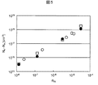
以下の表1〜表3に、異なる成長条件で形成した複数のβ−Ga2O3系単結晶膜12のSi濃度及びキャリア密度の測定結果を示す。

上記実施の形態によれば、HVPE法を用いてβ−Ga2O3系単結晶を成長させながらドーパントを添加することにより、MBE法やEFG法を用いる場合よりも広い範囲でβ−Ga2O3系単結晶のドーパントの濃度を制御することができる。また、イオン注入法を用いる場合のように、ドーパントの注入深さが限定されたり、イオンビームにより結晶性が劣化したりするという問題が生じない。
Claims (3)
- Ga2O3系基板の主面上に、HVPE法により、ドーパントをドーピングしながらβ−Ga2O3系単結晶膜を成長させる工程、
を含み、
前記ドーパントがSiであり、
前記ドーパントの原料ガスがSiCl4ガスであり、
前記β−Ga 2 O 3 系単結晶膜のGa原料ガスがGaClガスであり、
前記SiCl 4 ガスの供給分圧、前記GaClガスの供給分圧をそれぞれP 0 SiCl4 、P 0 GaCl としたとき、P 0 SiCl4 /(P 0 GaCl +P 0 SiCl4 )の値に基づいて前記β−Ga 2 O 3 系単結晶膜の前記ドーパントの濃度を濃度1×10 13 atoms/cm 3 以上5.0×10 20 atoms/cm 3 以下の範囲で制御する、
結晶積層構造体の製造方法。 - 前記P 0 SiCl4 /(P 0 GaCl +P 0 SiCl4 )の値に応じて、前記ドーパントの濃度を直線状に制御する、
請求項1に記載の結晶積層構造体の製造方法。 - 前記ドーパントの濃度を6.5×10¹⁵atoms/cm3以上2.1×1020atoms/cm3以下の範囲で制御する、
請求項1又は2に記載の結晶積層構造体の製造方法。
Priority Applications (7)
| Application Number | Priority Date | Filing Date | Title |
|---|---|---|---|
| JP2015058518A JP6376600B2 (ja) | 2015-03-20 | 2015-03-20 | 結晶積層構造体の製造方法 |
| PCT/JP2016/054620 WO2016152335A1 (ja) | 2015-03-20 | 2016-02-17 | 結晶積層構造体 |
| CN201680016988.8A CN107532326B (zh) | 2015-03-20 | 2016-02-17 | 晶体层叠结构体 |
| EP16768238.4A EP3272915B1 (en) | 2015-03-20 | 2016-02-17 | Method for providing a crystal laminate structure |
| US15/559,167 US10538862B2 (en) | 2015-03-20 | 2016-02-17 | Crystal laminate structure |
| TW105105677A TWI684662B (zh) | 2015-03-20 | 2016-02-25 | 結晶積層構造體 |
| US16/702,186 US11047067B2 (en) | 2015-03-20 | 2019-12-03 | Crystal laminate structure |
Applications Claiming Priority (1)
| Application Number | Priority Date | Filing Date | Title |
|---|---|---|---|
| JP2015058518A JP6376600B2 (ja) | 2015-03-20 | 2015-03-20 | 結晶積層構造体の製造方法 |
Publications (3)
| Publication Number | Publication Date |
|---|---|
| JP2016175807A JP2016175807A (ja) | 2016-10-06 |
| JP2016175807A5 JP2016175807A5 (ja) | 2017-03-09 |
| JP6376600B2 true JP6376600B2 (ja) | 2018-08-22 |
Family
ID=56977171
Family Applications (1)
| Application Number | Title | Priority Date | Filing Date |
|---|---|---|---|
| JP2015058518A Active JP6376600B2 (ja) | 2015-03-20 | 2015-03-20 | 結晶積層構造体の製造方法 |
Country Status (6)
| Country | Link |
|---|---|
| US (2) | US10538862B2 (ja) |
| EP (1) | EP3272915B1 (ja) |
| JP (1) | JP6376600B2 (ja) |
| CN (1) | CN107532326B (ja) |
| TW (1) | TWI684662B (ja) |
| WO (1) | WO2016152335A1 (ja) |
Families Citing this family (13)
| Publication number | Priority date | Publication date | Assignee | Title |
|---|---|---|---|---|
| JP6376600B2 (ja) * | 2015-03-20 | 2018-08-22 | 株式会社タムラ製作所 | 結晶積層構造体の製造方法 |
| WO2018052097A1 (ja) * | 2016-09-15 | 2018-03-22 | 株式会社Flosfia | 半導体膜の製造方法及び半導体膜並びにドーピング用錯化合物及びドーピング方法 |
| CN110325671A (zh) * | 2017-01-25 | 2019-10-11 | 中国科学院上海光学精密机械研究所 | 掺杂氧化镓晶态材料及其制备方法和应用 |
| JP7008293B2 (ja) * | 2017-04-27 | 2022-01-25 | 国立研究開発法人情報通信研究機構 | Ga2O3系半導体素子 |
| CN109423690B (zh) | 2017-08-21 | 2022-09-16 | 株式会社Flosfia | 用于制造结晶膜的方法 |
| JP7141849B2 (ja) | 2018-05-16 | 2022-09-26 | 株式会社サイオクス | 窒化物結晶基板および窒化物結晶基板の製造方法 |
| US11535951B1 (en) * | 2018-06-06 | 2022-12-27 | United States Of America As Represented By The Secretary Of The Air Force | Optimized thick heteroepitaxial growth of semiconductors with in-situ substrate pretreatment |
| CN110323291B (zh) * | 2019-04-22 | 2020-07-10 | 湖北大学 | 基于(GaY)2O3非晶薄膜的高增益日盲紫外光探测器及其制备方法 |
| KR20220052931A (ko) * | 2019-08-27 | 2022-04-28 | 신에쓰 가가꾸 고교 가부시끼가이샤 | 적층구조체 및 적층구조체의 제조방법 |
| JP7093329B2 (ja) * | 2019-09-02 | 2022-06-29 | 信越化学工業株式会社 | 積層構造体、半導体装置及び半導体システム |
| JP7097861B2 (ja) * | 2019-09-03 | 2022-07-08 | 信越化学工業株式会社 | 積層構造体、半導体装置及び半導体システム |
| JP2021170579A (ja) * | 2020-04-14 | 2021-10-28 | 株式会社ノベルクリスタルテクノロジー | 半導体膜及びその製造方法 |
| CN112853468A (zh) * | 2020-12-31 | 2021-05-28 | 杭州富加镓业科技有限公司 | 一种基于深度学习和热交换法的导电型氧化镓制备方法 |
Family Cites Families (15)
| Publication number | Priority date | Publication date | Assignee | Title |
|---|---|---|---|---|
| JP2001253794A (ja) * | 2000-03-10 | 2001-09-18 | Mitsubishi Chemicals Corp | 半導体バルク単結晶の製造方法 |
| JP4734786B2 (ja) * | 2001-07-04 | 2011-07-27 | 日亜化学工業株式会社 | 窒化ガリウム系化合物半導体基板、及びその製造方法 |
| US7008839B2 (en) * | 2002-03-08 | 2006-03-07 | Matsushita Electric Industrial Co., Ltd. | Method for manufacturing semiconductor thin film |
| JP2006193348A (ja) | 2005-01-11 | 2006-07-27 | Sumitomo Electric Ind Ltd | Iii族窒化物半導体基板およびその製造方法 |
| JP2009126723A (ja) | 2007-11-20 | 2009-06-11 | Sumitomo Electric Ind Ltd | Iii族窒化物半導体結晶の成長方法、iii族窒化物半導体結晶基板の製造方法およびiii族窒化物半導体結晶基板 |
| JP5392708B2 (ja) * | 2008-06-30 | 2014-01-22 | 国立大学法人東京農工大学 | ヘテロエピタキシャル成長方法 |
| US8822263B2 (en) | 2008-06-30 | 2014-09-02 | National University Corporation Tokyo University Of Agriculture And Technology | Epitaxial growth method of a zinc oxide based semiconductor layer, epitaxial crystal structure, epitaxial crystal growth apparatus, and semiconductor device |
| JP5948581B2 (ja) | 2011-09-08 | 2016-07-06 | 株式会社Flosfia | Ga2O3系半導体素子 |
| EP3151285B1 (en) | 2011-09-08 | 2023-11-22 | Tamura Corporation | Ga2o3-based semiconductor element |
| JP2013056803A (ja) | 2011-09-08 | 2013-03-28 | Tamura Seisakusho Co Ltd | β−Ga2O3系単結晶膜の製造方法 |
| WO2013035464A1 (ja) * | 2011-09-08 | 2013-03-14 | 株式会社タムラ製作所 | 結晶積層構造体及びその製造方法 |
| CN103765593B (zh) | 2011-09-08 | 2017-06-09 | 株式会社田村制作所 | Ga2O3系半导体元件 |
| JP5864998B2 (ja) | 2011-10-11 | 2016-02-17 | 株式会社タムラ製作所 | β−Ga2O3系単結晶の成長方法 |
| JP5984069B2 (ja) | 2013-09-30 | 2016-09-06 | 株式会社タムラ製作所 | β−Ga2O3系単結晶膜の成長方法、及び結晶積層構造体 |
| JP6376600B2 (ja) * | 2015-03-20 | 2018-08-22 | 株式会社タムラ製作所 | 結晶積層構造体の製造方法 |
-
2015
- 2015-03-20 JP JP2015058518A patent/JP6376600B2/ja active Active
-
2016
- 2016-02-17 CN CN201680016988.8A patent/CN107532326B/zh active Active
- 2016-02-17 WO PCT/JP2016/054620 patent/WO2016152335A1/ja active Application Filing
- 2016-02-17 EP EP16768238.4A patent/EP3272915B1/en active Active
- 2016-02-17 US US15/559,167 patent/US10538862B2/en active Active
- 2016-02-25 TW TW105105677A patent/TWI684662B/zh active
-
2019
- 2019-12-03 US US16/702,186 patent/US11047067B2/en active Active
Also Published As
| Publication number | Publication date |
|---|---|
| JP2016175807A (ja) | 2016-10-06 |
| WO2016152335A1 (ja) | 2016-09-29 |
| EP3272915B1 (en) | 2023-08-23 |
| CN107532326A (zh) | 2018-01-02 |
| US11047067B2 (en) | 2021-06-29 |
| TWI684662B (zh) | 2020-02-11 |
| CN107532326B (zh) | 2021-09-14 |
| US20200102667A1 (en) | 2020-04-02 |
| TW201641735A (zh) | 2016-12-01 |
| EP3272915A4 (en) | 2018-11-14 |
| US20180073164A1 (en) | 2018-03-15 |
| US10538862B2 (en) | 2020-01-21 |
| EP3272915A1 (en) | 2018-01-24 |
Similar Documents
| Publication | Publication Date | Title |
|---|---|---|
| JP6376600B2 (ja) | 結晶積層構造体の製造方法 | |
| JP5984069B2 (ja) | β−Ga2O3系単結晶膜の成長方法、及び結晶積層構造体 | |
| US8795624B2 (en) | Monocrystalline silicon carbide ingot, monocrystalline silicon carbide wafer and method of manufacturing the same | |
| CN107534062B (zh) | 高耐压肖特基势垒二极管 | |
| US10985016B2 (en) | Semiconductor substrate, and epitaxial wafer and method for producing same | |
| JP6875708B2 (ja) | 結晶積層構造体、及びそれを製造する方法 | |
| CN106471163B (zh) | 半导体衬底、外延片及其制造方法 | |
| EP3929336A1 (en) | Gan crystal and substrate | |
| JPWO2015005064A1 (ja) | 炭化珪素半導体装置の製造方法および炭化珪素半導体装置 | |
| JP2005306723A (ja) | 窒化ガリウム基板、エピタキシャル基板、および窒化ガリウムを形成する方法 | |
| JP2012111677A (ja) | Iii族窒化物結晶の製造方法、iii族窒化物テンプレートの製造方法、iii族窒化物結晶及びiii族窒化物テンプレート | |
| WO2022059669A1 (ja) | β-Ga2O3系単結晶膜及びその製造方法 |
Legal Events
| Date | Code | Title | Description |
|---|---|---|---|
| A521 | Request for written amendment filed |
Free format text: JAPANESE INTERMEDIATE CODE: A523 Effective date: 20170203 |
|
| A621 | Written request for application examination |
Free format text: JAPANESE INTERMEDIATE CODE: A621 Effective date: 20170309 |
|
| A521 | Request for written amendment filed |
Free format text: JAPANESE INTERMEDIATE CODE: A821 Effective date: 20170309 |
|
| A871 | Explanation of circumstances concerning accelerated examination |
Free format text: JAPANESE INTERMEDIATE CODE: A871 Effective date: 20170419 |
|
| RD02 | Notification of acceptance of power of attorney |
Free format text: JAPANESE INTERMEDIATE CODE: A7422 Effective date: 20170419 |
|
| A521 | Request for written amendment filed |
Free format text: JAPANESE INTERMEDIATE CODE: A821 Effective date: 20170421 |
|
| A975 | Report on accelerated examination |
Free format text: JAPANESE INTERMEDIATE CODE: A971005 Effective date: 20170630 |
|
| A131 | Notification of reasons for refusal |
Free format text: JAPANESE INTERMEDIATE CODE: A131 Effective date: 20170711 |
|
| A601 | Written request for extension of time |
Free format text: JAPANESE INTERMEDIATE CODE: A601 Effective date: 20170907 |
|
| A521 | Request for written amendment filed |
Free format text: JAPANESE INTERMEDIATE CODE: A523 Effective date: 20171019 |
|
| A131 | Notification of reasons for refusal |
Free format text: JAPANESE INTERMEDIATE CODE: A131 Effective date: 20180109 |
|
| A601 | Written request for extension of time |
Free format text: JAPANESE INTERMEDIATE CODE: A601 Effective date: 20180307 |
|
| RD04 | Notification of resignation of power of attorney |
Free format text: JAPANESE INTERMEDIATE CODE: A7424 Effective date: 20180327 |
|
| A521 | Request for written amendment filed |
Free format text: JAPANESE INTERMEDIATE CODE: A523 Effective date: 20180419 |
|
| TRDD | Decision of grant or rejection written | ||
| A01 | Written decision to grant a patent or to grant a registration (utility model) |
Free format text: JAPANESE INTERMEDIATE CODE: A01 Effective date: 20180703 |
|
| A61 | First payment of annual fees (during grant procedure) |
Free format text: JAPANESE INTERMEDIATE CODE: A61 Effective date: 20180719 |
|
| R150 | Certificate of patent or registration of utility model |
Ref document number: 6376600 Country of ref document: JP Free format text: JAPANESE INTERMEDIATE CODE: R150 |
|
| R250 | Receipt of annual fees |
Free format text: JAPANESE INTERMEDIATE CODE: R250 |
|
| R250 | Receipt of annual fees |
Free format text: JAPANESE INTERMEDIATE CODE: R250 |
|
| R250 | Receipt of annual fees |
Free format text: JAPANESE INTERMEDIATE CODE: R250 |