JP6310312B2 - 光電変換素子およびその製造方法 - Google Patents
光電変換素子およびその製造方法 Download PDFInfo
- Publication number
- JP6310312B2 JP6310312B2 JP2014086800A JP2014086800A JP6310312B2 JP 6310312 B2 JP6310312 B2 JP 6310312B2 JP 2014086800 A JP2014086800 A JP 2014086800A JP 2014086800 A JP2014086800 A JP 2014086800A JP 6310312 B2 JP6310312 B2 JP 6310312B2
- Authority
- JP
- Japan
- Prior art keywords
- photoelectric conversion
- layer
- conversion element
- element according
- particles
- Prior art date
- Legal status (The legal status is an assumption and is not a legal conclusion. Google has not performed a legal analysis and makes no representation as to the accuracy of the status listed.)
- Expired - Fee Related
Links
Images

Classifications
-
- H—ELECTRICITY
- H10—SEMICONDUCTOR DEVICES; ELECTRIC SOLID-STATE DEVICES NOT OTHERWISE PROVIDED FOR
- H10F—INORGANIC SEMICONDUCTOR DEVICES SENSITIVE TO INFRARED RADIATION, LIGHT, ELECTROMAGNETIC RADIATION OF SHORTER WAVELENGTH OR CORPUSCULAR RADIATION
- H10F39/00—Integrated devices, or assemblies of multiple devices, comprising at least one element covered by group H10F30/00, e.g. radiation detectors comprising photodiode arrays
- H10F39/011—Manufacture or treatment of image sensors covered by group H10F39/12
- H10F39/024—Manufacture or treatment of image sensors covered by group H10F39/12 of coatings or optical elements
-
- H—ELECTRICITY
- H10—SEMICONDUCTOR DEVICES; ELECTRIC SOLID-STATE DEVICES NOT OTHERWISE PROVIDED FOR
- H10F—INORGANIC SEMICONDUCTOR DEVICES SENSITIVE TO INFRARED RADIATION, LIGHT, ELECTROMAGNETIC RADIATION OF SHORTER WAVELENGTH OR CORPUSCULAR RADIATION
- H10F39/00—Integrated devices, or assemblies of multiple devices, comprising at least one element covered by group H10F30/00, e.g. radiation detectors comprising photodiode arrays
- H10F39/10—Integrated devices
- H10F39/12—Image sensors
- H10F39/18—Complementary metal-oxide-semiconductor [CMOS] image sensors; Photodiode array image sensors
-
- H—ELECTRICITY
- H10—SEMICONDUCTOR DEVICES; ELECTRIC SOLID-STATE DEVICES NOT OTHERWISE PROVIDED FOR
- H10F—INORGANIC SEMICONDUCTOR DEVICES SENSITIVE TO INFRARED RADIATION, LIGHT, ELECTROMAGNETIC RADIATION OF SHORTER WAVELENGTH OR CORPUSCULAR RADIATION
- H10F39/00—Integrated devices, or assemblies of multiple devices, comprising at least one element covered by group H10F30/00, e.g. radiation detectors comprising photodiode arrays
- H10F39/80—Constructional details of image sensors
- H10F39/806—Optical elements or arrangements associated with the image sensors
Landscapes
- Solid State Image Pick-Up Elements (AREA)
- Drying Of Semiconductors (AREA)
- Light Receiving Elements (AREA)
Description
前記半導体基板の前記光電変換部と前記周辺回路部の少なくとも一部との上に設けられた第1層と、 前記第1層の上に設けられており、有機物および前記有機物に分散した粒子を含み、表面粗さがRMS50nm以上である第2層と、を備え、前記第1層は、前記周辺回路部に設けられた電極パッドの上方に位置する部分に開口を有し、前記第2層は、前記電極パッドの上方に位置する部分と前記光電変換部の上方に位置する部分とに開口を有することを特徴とする。
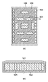
本実施例の光電変換素子を図1により説明する。光電変換素子100は、光電変換部が配置された光電変換領域101、反射防止領域102、電極パッドが配置された電極パッド領域103を有している。光電変換部は、光を電気信号に変換する。反射防止領域102は、光電変換領域101と電極パッド領域103以外の領域に設けられている。反射防止領域102は後述する反射防止層で覆われている。例えば光電変換部の一部の遮光された領域や、光電変換部から信号を読み出すための駆動や読み出した信号の処理等を行う周辺回路部などが配置された領域は反射防止領域102である。本実施例の光電変換領域101は、例えば図1(b)に示すような、複数の光電変換部104が一次元に配置されたAFセンサーやイメージセンサなどである。
・圧力:15 mTorr
・高周波電力:500 W
・エッチングガス:CF4/O2=100/10 sccm
・時間:60sec
エッチング条件は、圧力が1〜100mTorrの範囲内、高周波電力が100〜1000Wの範囲内、エッチングガスとしてCF4及びO2を、流量をそれぞれ0〜500sccm及び1〜500sccmの範囲内で用いればよい。
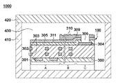
次に、実施例2について図4により説明する。図4は、図1のA−A’の線に対応した光電変換素子100の一部の断面を示す。実施例1と同じ構成には同じ参照番号を付し、重複する説明は省略する。実施例1と同じく、図4(a)に示すように、フォトダイオード301や周辺回路(不図示)などが形成された半導体基板300に層間絶縁膜302、配線303などが形成された部材を準備する。次に、部材にパッシベーション層305を形成し、その後、開口306を形成する。
・圧力:15 mTorr
・高周波電力:500 W
・エッチングガス:O2/N2/Ar=80/20/100 sccm
・時間:60sec
エッチング条件は、圧力が1〜100mTorrの範囲内、高周波電力が100〜1000Wの範囲内、エッチングガスとしてO2、N2及びArを、流量をそれぞれ0〜100sccm、1〜50sccm及び1〜200sccmの範囲内であればよい。
Claims (19)
- 光電変換部および周辺回路部を有する部材の上に、前記光電変換部と前記周辺回路部の少なくとも一部とを覆うように第1層を形成する工程と、
前記第1層の上に、前記光電変換部および前記周辺回路部を覆うように、有機物および前記有機物中に分散した粒子を含む膜を形成する工程と、
前記膜のうち前記光電変換部の上方に位置する部分を少なくとも除去することによって、前記膜から第2層を形成する工程と、
前記第2層を形成した後に、前記第1層をエッチング阻止層としたドライエッチングにより前記第2層の表面を粗面化する工程と、を含むことを特徴とする光電変換素子の製造方法。 - 前記ドライエッチングにより前記第2層の表面に前記粒子を露出させることを特徴とする請求項1に記載の光電変換素子の製造方法。
- 前記膜をパターニングすることにより、前記第2層を形成することを特徴とする請求項1又は2に記載の光電変換素子の製造方法。
- 前記膜は感光性を有しており、前記膜の露光および現像によって前記膜をパターニングすることを特徴とする請求項3に記載の光電変換素子の製造方法。
- 前記粒子が分散した有機材料を塗布することにより、前記膜を形成することを特徴とする請求項1乃至4の何れか1項に記載の光電変換素子の製造方法。
- 前記ドライエッチングは、1〜100mTorrの範囲内の圧力、100〜1000Wの範囲内の高周波電力で、エッチングガスとして流量が0〜500sccmのCF4及び流量が1〜500sccmのO2を使用して行われることを特徴とする請求項1乃至5のいずれか1項に記載の光電変換素子の製造方法。
- 前記ドライエッチングでは、前記第2層をマスクとして前記第2層の下地をパターニングすることを特徴とする請求項1乃至6のいずれか1項に記載の光電変換素子の製造方法。
- 前記ドライエッチングは、1〜100mTorrの範囲内の圧力、100〜1000Wの範囲内の高周波電力で、エッチングガスとして流量が0〜100sccmのO2、流量が1〜50sccmのN2及び流量が1〜200sccmのArを使用して行われることを特徴とする請求項1乃至7のいずれか1項に記載の光電変換素子の製造方法。
- 前記粒子は、顔料であることを特徴とする請求項1乃至8のいずれか1項に記載の光電変換素子の製造方法。
- 前記粒子の粒径はメジアン径で30〜100nmであることを特徴とする請求項1乃至9のいずれか1項に記載の光電変換素子の製造方法。
- 前記有機物のエッチング選択性と前記粒子のエッチング選択性とは異なることを特徴とする請求項1乃至10のいずれか1項に記載の光電変換素子の製造方法。
- 前記膜を形成する前に、前記第1層の上に、前記光電変換部および前記周辺回路部を覆うように第3層を形成する工程を更に有することを特徴とする請求項1乃至11のいずれか1項に記載の光電変換素子の製造方法。
- 前記ドライエッチングによって、前記第3層のうち前記光電変換部の上方に位置する部分を少なくとも除去することを特徴とする請求項12に記載の光電変換素子の製造方法。
- 光電変換部および周辺回路部を有する半導体基板と、
前記半導体基板の前記光電変換部と前記周辺回路部の少なくとも一部との上に設けられた第1層と、
前記第1層の上に設けられており、有機物および前記有機物に分散した粒子を含み、表面粗さがRMS50nm以上である第2層と、を備え、
前記第1層は、前記周辺回路部に設けられた電極パッドの上方に位置する部分に開口を有し、
前記第2層は、前記電極パッドの上方に位置する部分と前記光電変換部の上方に位置する部分とに開口を有することを特徴とする光電変換素子。 - 前記第2層が前記光電変換素子の表面を構成することを特徴とする請求項14に記載の光電変換素子。
- 前記粒子は、顔料であることを特徴とする請求項14または15に記載の光電変換素子。
- 前記粒子の粒径はメジアン径で30〜100nmであることを特徴とする請求項14乃至16のいずれか1項に記載の光電変換素子。
- 前記第1層と前記第2層との間に、前記光電変換部および前記周辺回路部を覆う第3層を更に備えることを特徴とする請求項14乃至17のいずれか1項に記載の光電変換素子。
- 前記第3層は、前記電極パッドの上方に位置する部分と前記光電変換部の上方に位置する部分とに開口を有することを特徴とする請求項18に記載の光電変換素子。
Priority Applications (2)
| Application Number | Priority Date | Filing Date | Title |
|---|---|---|---|
| JP2014086800A JP6310312B2 (ja) | 2014-04-18 | 2014-04-18 | 光電変換素子およびその製造方法 |
| US14/680,291 US9502460B2 (en) | 2014-04-18 | 2015-04-07 | Photoelectric conversion element and method of manufacturing the same |
Applications Claiming Priority (1)
| Application Number | Priority Date | Filing Date | Title |
|---|---|---|---|
| JP2014086800A JP6310312B2 (ja) | 2014-04-18 | 2014-04-18 | 光電変換素子およびその製造方法 |
Publications (3)
| Publication Number | Publication Date |
|---|---|
| JP2015207638A JP2015207638A (ja) | 2015-11-19 |
| JP2015207638A5 JP2015207638A5 (ja) | 2017-05-25 |
| JP6310312B2 true JP6310312B2 (ja) | 2018-04-11 |
Family
ID=54322678
Family Applications (1)
| Application Number | Title | Priority Date | Filing Date |
|---|---|---|---|
| JP2014086800A Expired - Fee Related JP6310312B2 (ja) | 2014-04-18 | 2014-04-18 | 光電変換素子およびその製造方法 |
Country Status (2)
| Country | Link |
|---|---|
| US (1) | US9502460B2 (ja) |
| JP (1) | JP6310312B2 (ja) |
Families Citing this family (7)
| Publication number | Priority date | Publication date | Assignee | Title |
|---|---|---|---|---|
| JP6168915B2 (ja) * | 2013-08-22 | 2017-07-26 | キヤノン株式会社 | 半導体装置の製造方法 |
| EP3724920B1 (en) * | 2017-12-12 | 2022-05-11 | LFoundry S.r.l. | Semiconductor optical sensor for visible and ultraviolet light detection and corresponding manufacturing process |
| KR102633533B1 (ko) * | 2018-11-09 | 2024-02-06 | 주식회사 엘지화학 | 파라데이 상자를 이용한 플라즈마 식각 방법 |
| US11661332B2 (en) * | 2019-02-20 | 2023-05-30 | Invensense, Inc. | Stiction reduction system and method thereof |
| TWI856837B (zh) * | 2019-03-21 | 2024-09-21 | 美商應用材料股份有限公司 | 監視化學機械拋光中的拋光墊紋理 |
| JP2021150473A (ja) * | 2020-03-19 | 2021-09-27 | ソニーセミコンダクタソリューションズ株式会社 | 固体撮像装置及び電子機器 |
| JP7624806B2 (ja) * | 2020-04-03 | 2025-01-31 | 浜松ホトニクス株式会社 | 固体撮像装置 |
Family Cites Families (20)
| Publication number | Priority date | Publication date | Assignee | Title |
|---|---|---|---|---|
| JPH01164073A (ja) * | 1987-09-11 | 1989-06-28 | Canon Inc | 光電変換装置 |
| JP2774006B2 (ja) * | 1991-12-25 | 1998-07-09 | 三菱電機株式会社 | 半導体受光装置及びその製造方法 |
| JPH06302845A (ja) * | 1993-04-19 | 1994-10-28 | Olympus Optical Co Ltd | 反射防止膜の形成方法 |
| JP3921952B2 (ja) | 2001-02-28 | 2007-05-30 | 凸版印刷株式会社 | 撮像素子及びその製造方法 |
| TWI234885B (en) * | 2002-03-26 | 2005-06-21 | Fujikura Ltd | Electroconductive glass and photovoltaic cell using the same |
| JP4587772B2 (ja) * | 2004-10-22 | 2010-11-24 | イビデン株式会社 | 多層プリント配線板 |
| US7687326B2 (en) * | 2004-12-17 | 2010-03-30 | Semiconductor Energy Laboratory Co., Ltd. | Semiconductor device and manufacturing method thereof |
| US7977669B2 (en) * | 2005-02-10 | 2011-07-12 | Semiconductor Energy Laboratory Co., Ltd. | Semiconductor memory device having a liquid-repellent layer |
| JP2007053153A (ja) * | 2005-08-16 | 2007-03-01 | Toppan Printing Co Ltd | 固体撮像素子及びその製造方法 |
| JP2009168872A (ja) * | 2008-01-11 | 2009-07-30 | Sony Corp | レンズの製造方法および固体撮像装置の製造方法 |
| JP2009283902A (ja) | 2008-04-25 | 2009-12-03 | Panasonic Corp | 光学デバイスとこれを備えた電子機器 |
| JP2010085754A (ja) * | 2008-09-30 | 2010-04-15 | Fujifilm Corp | カラーフィルタの製造方法及び固体撮像装置 |
| JP2010134228A (ja) * | 2008-12-05 | 2010-06-17 | Fujifilm Corp | カラーフィルタの製造方法及び固体撮像装置 |
| JP5446387B2 (ja) * | 2009-03-31 | 2014-03-19 | ソニー株式会社 | 反射防止構造体の製造方法および固体撮像装置の製造方法 |
| JP2010272612A (ja) * | 2009-05-20 | 2010-12-02 | Sony Corp | 固体撮像装置とその製造方法および撮像装置 |
| JP5657337B2 (ja) * | 2009-10-19 | 2015-01-21 | 富士フイルム株式会社 | ウエハレベルレンズ用チタンブラック分散物、それを含有する感光性樹脂組成物、及び、ウエハレベルレンズ |
| US8268058B2 (en) * | 2009-11-16 | 2012-09-18 | Fu-Chi Wu | High-performance labyrinth type air treatment apparatus |
| JP2012204402A (ja) * | 2011-03-23 | 2012-10-22 | Toshiba Corp | 固体撮像装置及びその製造方法 |
| JP2012203083A (ja) * | 2011-03-24 | 2012-10-22 | Sumitomo Osaka Cement Co Ltd | 可視近赤外光遮蔽黒色膜、可視近赤外光遮蔽黒色膜付き基材、及び固体撮像素子 |
| JP5681597B2 (ja) * | 2011-09-20 | 2015-03-11 | 富士フイルム株式会社 | 固体撮像素子の製造方法 |
-
2014
- 2014-04-18 JP JP2014086800A patent/JP6310312B2/ja not_active Expired - Fee Related
-
2015
- 2015-04-07 US US14/680,291 patent/US9502460B2/en not_active Expired - Fee Related
Also Published As
| Publication number | Publication date |
|---|---|
| US20150303226A1 (en) | 2015-10-22 |
| US9502460B2 (en) | 2016-11-22 |
| JP2015207638A (ja) | 2015-11-19 |
Similar Documents
| Publication | Publication Date | Title |
|---|---|---|
| JP6310312B2 (ja) | 光電変換素子およびその製造方法 | |
| TWI278991B (en) | Solid image-pickup device and method of manufacturing the same | |
| JP2001208902A (ja) | 固体撮像素子及びその製造方法 | |
| US10178286B2 (en) | Method for forming color filter array, method for manufacturing imaging apparatus, and imaging apparatus | |
| KR100664790B1 (ko) | 이미지 센서의 제조 방법 | |
| US7898049B2 (en) | Touching microlens structure for a pixel sensor and method of fabrication | |
| TW202236696A (zh) | 光譜芯片及其製備方法、光譜分析裝置 | |
| CN102270651B (zh) | 装置和图像传感器 | |
| JP2007053153A (ja) | 固体撮像素子及びその製造方法 | |
| JP2011171328A (ja) | 固体撮像素子およびその製造方法 | |
| CN106298829A (zh) | 一种金属栅格的形成方法 | |
| JP5836637B2 (ja) | パターン形成方法、固体撮像装置及び固体撮像装置の製造方法 | |
| JP2000307090A (ja) | 固体撮像素子用マイクロレンズアレイ及びそれを用いた固体撮像素子並びにそれらの製造方法 | |
| TW201944585A (zh) | 光學感測器及其形成方法 | |
| JP4175169B2 (ja) | 固体撮像素子及びその製造方法 | |
| JPH01270362A (ja) | 固体撮像装置の製造方法 | |
| JP4984400B2 (ja) | 固体撮像素子及びその製造方法 | |
| JP2017118065A (ja) | 固体撮像素子およびその製造方法 | |
| JP2009152314A (ja) | イメージセンサーおよびその製造方法 | |
| CN100405606C (zh) | 具有减小应力的滤色层的图像传感器及其制造方法 | |
| JPH06302794A (ja) | 固体撮像素子の製法 | |
| JP6499741B2 (ja) | 光学センサおよびその製造方法 | |
| KR20100057993A (ko) | 이미지 센서 및 그 제조방법 | |
| JP2006190944A (ja) | 画像センサ・ダイ | |
| JP2016219703A (ja) | 固体撮像素子及び固体撮像素子の製造方法 |
Legal Events
| Date | Code | Title | Description |
|---|---|---|---|
| A521 | Request for written amendment filed |
Free format text: JAPANESE INTERMEDIATE CODE: A523 Effective date: 20170404 |
|
| A621 | Written request for application examination |
Free format text: JAPANESE INTERMEDIATE CODE: A621 Effective date: 20170404 |
|
| A977 | Report on retrieval |
Free format text: JAPANESE INTERMEDIATE CODE: A971007 Effective date: 20171109 |
|
| A131 | Notification of reasons for refusal |
Free format text: JAPANESE INTERMEDIATE CODE: A131 Effective date: 20171117 |
|
| A521 | Request for written amendment filed |
Free format text: JAPANESE INTERMEDIATE CODE: A523 Effective date: 20180116 |
|
| TRDD | Decision of grant or rejection written | ||
| A01 | Written decision to grant a patent or to grant a registration (utility model) |
Free format text: JAPANESE INTERMEDIATE CODE: A01 Effective date: 20180216 |
|
| A61 | First payment of annual fees (during grant procedure) |
Free format text: JAPANESE INTERMEDIATE CODE: A61 Effective date: 20180316 |
|
| R151 | Written notification of patent or utility model registration |
Ref document number: 6310312 Country of ref document: JP Free format text: JAPANESE INTERMEDIATE CODE: R151 |
|
| LAPS | Cancellation because of no payment of annual fees |