JP6310312B2 - Photoelectric conversion element and manufacturing method thereof - Google Patents
Photoelectric conversion element and manufacturing method thereof Download PDFInfo
- Publication number
- JP6310312B2 JP6310312B2 JP2014086800A JP2014086800A JP6310312B2 JP 6310312 B2 JP6310312 B2 JP 6310312B2 JP 2014086800 A JP2014086800 A JP 2014086800A JP 2014086800 A JP2014086800 A JP 2014086800A JP 6310312 B2 JP6310312 B2 JP 6310312B2
- Authority
- JP
- Japan
- Prior art keywords
- photoelectric conversion
- layer
- conversion element
- element according
- particles
- Prior art date
- Legal status (The legal status is an assumption and is not a legal conclusion. Google has not performed a legal analysis and makes no representation as to the accuracy of the status listed.)
- Expired - Fee Related
Links
- 238000006243 chemical reaction Methods 0.000 title claims description 99
- 238000004519 manufacturing process Methods 0.000 title claims description 19
- 239000002245 particle Substances 0.000 claims description 35
- 238000005530 etching Methods 0.000 claims description 27
- 239000011368 organic material Substances 0.000 claims description 25
- 230000002093 peripheral effect Effects 0.000 claims description 19
- 239000000126 substance Substances 0.000 claims description 16
- 238000000034 method Methods 0.000 claims description 14
- 239000000049 pigment Substances 0.000 claims description 14
- 238000001312 dry etching Methods 0.000 claims description 10
- 230000003746 surface roughness Effects 0.000 claims description 10
- 238000007788 roughening Methods 0.000 claims description 9
- 239000004065 semiconductor Substances 0.000 claims description 8
- 239000000758 substrate Substances 0.000 claims description 8
- 230000000903 blocking effect Effects 0.000 claims description 2
- 238000000059 patterning Methods 0.000 claims description 2
- 206010034972 Photosensitivity reaction Diseases 0.000 claims 1
- 239000004744 fabric Substances 0.000 claims 1
- 239000005416 organic matter Substances 0.000 claims 1
- 230000036211 photosensitivity Effects 0.000 claims 1
- 239000010410 layer Substances 0.000 description 88
- 239000006185 dispersion Substances 0.000 description 19
- 238000002161 passivation Methods 0.000 description 14
- 239000011229 interlayer Substances 0.000 description 7
- 239000007789 gas Substances 0.000 description 6
- 239000000463 material Substances 0.000 description 5
- 230000000694 effects Effects 0.000 description 4
- 239000011347 resin Substances 0.000 description 3
- 229920005989 resin Polymers 0.000 description 3
- 239000004925 Acrylic resin Substances 0.000 description 2
- 229920000178 Acrylic resin Polymers 0.000 description 2
- VYPSYNLAJGMNEJ-UHFFFAOYSA-N Silicium dioxide Chemical compound O=[Si]=O VYPSYNLAJGMNEJ-UHFFFAOYSA-N 0.000 description 2
- GWEVSGVZZGPLCZ-UHFFFAOYSA-N Titan oxide Chemical compound O=[Ti]=O GWEVSGVZZGPLCZ-UHFFFAOYSA-N 0.000 description 2
- 238000010586 diagram Methods 0.000 description 2
- 239000007788 liquid Substances 0.000 description 2
- 230000003287 optical effect Effects 0.000 description 2
- PNEYBMLMFCGWSK-UHFFFAOYSA-N aluminium oxide Inorganic materials [O-2].[O-2].[O-2].[Al+3].[Al+3] PNEYBMLMFCGWSK-UHFFFAOYSA-N 0.000 description 1
- 230000015572 biosynthetic process Effects 0.000 description 1
- 239000011248 coating agent Substances 0.000 description 1
- 238000000576 coating method Methods 0.000 description 1
- 238000001514 detection method Methods 0.000 description 1
- 239000002612 dispersion medium Substances 0.000 description 1
- 238000001035 drying Methods 0.000 description 1
- 238000003384 imaging method Methods 0.000 description 1
- 239000001023 inorganic pigment Substances 0.000 description 1
- 230000007257 malfunction Effects 0.000 description 1
- 238000005259 measurement Methods 0.000 description 1
- 239000011146 organic particle Substances 0.000 description 1
- 239000012860 organic pigment Substances 0.000 description 1
- 238000000206 photolithography Methods 0.000 description 1
- 239000000377 silicon dioxide Substances 0.000 description 1
- 238000004528 spin coating Methods 0.000 description 1
- 239000002344 surface layer Substances 0.000 description 1
- 239000012780 transparent material Substances 0.000 description 1
Images

Classifications
-
- H—ELECTRICITY
- H01—ELECTRIC ELEMENTS
- H01L—SEMICONDUCTOR DEVICES NOT COVERED BY CLASS H10
- H01L27/00—Devices consisting of a plurality of semiconductor or other solid-state components formed in or on a common substrate
- H01L27/14—Devices consisting of a plurality of semiconductor or other solid-state components formed in or on a common substrate including semiconductor components sensitive to infrared radiation, light, electromagnetic radiation of shorter wavelength or corpuscular radiation and specially adapted either for the conversion of the energy of such radiation into electrical energy or for the control of electrical energy by such radiation
- H01L27/144—Devices controlled by radiation
- H01L27/146—Imager structures
- H01L27/14683—Processes or apparatus peculiar to the manufacture or treatment of these devices or parts thereof
- H01L27/14685—Process for coatings or optical elements
-
- H—ELECTRICITY
- H01—ELECTRIC ELEMENTS
- H01L—SEMICONDUCTOR DEVICES NOT COVERED BY CLASS H10
- H01L27/00—Devices consisting of a plurality of semiconductor or other solid-state components formed in or on a common substrate
- H01L27/14—Devices consisting of a plurality of semiconductor or other solid-state components formed in or on a common substrate including semiconductor components sensitive to infrared radiation, light, electromagnetic radiation of shorter wavelength or corpuscular radiation and specially adapted either for the conversion of the energy of such radiation into electrical energy or for the control of electrical energy by such radiation
- H01L27/144—Devices controlled by radiation
- H01L27/146—Imager structures
- H01L27/14601—Structural or functional details thereof
- H01L27/14625—Optical elements or arrangements associated with the device
-
- H—ELECTRICITY
- H01—ELECTRIC ELEMENTS
- H01L—SEMICONDUCTOR DEVICES NOT COVERED BY CLASS H10
- H01L27/00—Devices consisting of a plurality of semiconductor or other solid-state components formed in or on a common substrate
- H01L27/14—Devices consisting of a plurality of semiconductor or other solid-state components formed in or on a common substrate including semiconductor components sensitive to infrared radiation, light, electromagnetic radiation of shorter wavelength or corpuscular radiation and specially adapted either for the conversion of the energy of such radiation into electrical energy or for the control of electrical energy by such radiation
- H01L27/144—Devices controlled by radiation
- H01L27/146—Imager structures
- H01L27/14643—Photodiode arrays; MOS imagers
Description
本発明は、光電変換素子および光電変換素子の製造方法に関する。 The present invention relates to a photoelectric conversion element and a method for manufacturing the photoelectric conversion element.
光電変換素子のフォトダイオードが配置される画素アレイ部に、光が入射する領域と遮光された領域とを設けた光電変換素子がある。遮光された領域はオプティカルブラック領域(OB)とも呼ばれ、イメージセンサの基準となる信号を発生するための領域として使用される。遮光された領域の表面に凸凹を形成したものがある。特許文献1では、配線のためのパッド部分を開口するためにイメージセンサの表面をエッチングするとき、同時に遮光された領域の上方の領域をエッチングして凸凹な表面を形成することが開示されている。 There is a photoelectric conversion element in which a light incident region and a light-shielded region are provided in a pixel array portion where a photodiode of the photoelectric conversion element is disposed. The shaded area is also called an optical black area (OB), and is used as an area for generating a signal serving as a reference for the image sensor. There is one in which unevenness is formed on the surface of the shielded region. Patent Document 1 discloses that when etching the surface of an image sensor to open a pad portion for wiring, a region above the light-shielded region is simultaneously etched to form an uneven surface. .
特許文献1では、遮光された領域の表面はマイクロレンズと同じ材料で形成されているので、エッチングにより表面に凸凹を形成する上で、好適なエッチング条件が見いだせなかった。そのためにマイクロレンズ部分にレジストマスクを用意する等の工程が増え、エッチング工程が長くなった。本発明は、光電変換素子の上の層の表面での光の反射の影響を低減する光電変換素子およびその製造方法を提供することを目的とする。 In Patent Document 1, since the surface of the light-shielded region is formed of the same material as the microlens, no suitable etching conditions were found for forming irregularities on the surface by etching. Therefore, the number of processes such as preparing a resist mask in the microlens portion has increased, and the etching process has become longer. An object of this invention is to provide the photoelectric conversion element which reduces the influence of the reflection of the light in the surface of the layer on a photoelectric conversion element, and its manufacturing method.
本発明の光電変換素子の製造方法は、光電変換部および周辺回路部を有する部材の上に、前記光電変換部と前記周辺回路部の少なくとも一部とを覆うように第1層を形成する工程と、前記第1層の上に、前記光電変換部および前記周辺回路部を覆うように、有機物および前記有機物中に分散した粒子を含む膜を形成する工程と、前記膜のうち前記光電変換部の上方に位置する部分を少なくとも除去することによって、前記膜から第2層を形成する工程と、ドライエッチングにより前記第2層の表面を粗面化する工程とを含むことを特徴とする。 In the method for producing a photoelectric conversion element of the present invention, a step of forming a first layer on a member having a photoelectric conversion unit and a peripheral circuit unit so as to cover at least a part of the photoelectric conversion unit and the peripheral circuit unit. And forming a film containing an organic substance and particles dispersed in the organic substance so as to cover the photoelectric conversion part and the peripheral circuit part on the first layer, and the photoelectric conversion part of the film The method includes a step of forming a second layer from the film by removing at least a portion located above and a step of roughening the surface of the second layer by dry etching.
また、本発明の光電変換素子は、光電変換部および周辺回路部を有する半導体基板と、
前記半導体基板の前記光電変換部と前記周辺回路部の少なくとも一部との上に設けられた第1層と、 前記第1層の上に設けられており、有機物および前記有機物に分散した粒子を含み、表面粗さがRMS50nm以上である第2層と、を備え、前記第1層は、前記周辺回路部に設けられた電極パッドの上方に位置する部分に開口を有し、前記第2層は、前記電極パッドの上方に位置する部分と前記光電変換部の上方に位置する部分とに開口を有することを特徴とする。
Further, the photoelectric conversion element of the present invention includes a semiconductor substrate having a photoelectric conversion part and a peripheral circuit part ,
A first layer provided on the photoelectric conversion part and at least a part of the peripheral circuit part of the semiconductor substrate; and an organic substance and particles dispersed in the organic substance provided on the first layer. And a second layer having a surface roughness of RMS 50 nm or more , wherein the first layer has an opening in a portion located above the electrode pad provided in the peripheral circuit portion, and the second layer Has an opening in a portion located above the electrode pad and a portion located above the photoelectric conversion unit .
本発明によれば、光電変換部の上の層の表面での光の反射の影響を低減する光電変換素子及びその製造方法を提供することができる。 ADVANTAGE OF THE INVENTION According to this invention, the photoelectric conversion element which reduces the influence of the reflection of the light in the surface of the layer on a photoelectric conversion part, and its manufacturing method can be provided.
[実施例1]
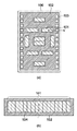
本実施例の光電変換素子を図1により説明する。光電変換素子100は、光電変換部が配置された光電変換領域101、反射防止領域102、電極パッドが配置された電極パッド領域103を有している。光電変換部は、光を電気信号に変換する。反射防止領域102は、光電変換領域101と電極パッド領域103以外の領域に設けられている。反射防止領域102は後述する反射防止層で覆われている。例えば光電変換部の一部の遮光された領域や、光電変換部から信号を読み出すための駆動や読み出した信号の処理等を行う周辺回路部などが配置された領域は反射防止領域102である。本実施例の光電変換領域101は、例えば図1(b)に示すような、複数の光電変換部104が一次元に配置されたAFセンサーやイメージセンサなどである。
[Example 1]
The photoelectric conversion element of this example will be described with reference to FIG. The
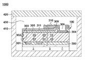
次に、本実施例の光電変換素子を備える光電変換装置について図2により説明する。図2では、図1(a)のA−A’の線に対応した光電変換素子100の一部の断面を示す。光電変換部301や周辺回路(不図示)などが形成された半導体基板300に層間絶縁膜302、配線303などが形成された部材が示されている。説明の便宜上、この部材を図2に示すように、3つの領域A,B,C分ける。領域Aは、半導体基板300にフォトダイオードなどの光電変換部301が複数形成されており、光が入射される開口を有する領域である。領域Bは、光電変換部301の一部が遮光されたオプティカルブラック部(OB部)や、光電変換部301から信号を読み出すための駆動、読み出した信号の処理等を行う周辺回路部などが形成されている領域である。領域Cは、層間絶縁膜302の表面に電極パッド304が配置されている領域である。領域Aは、図1(a)の光電変換領域101に対応し、領域Bは図1(a)の反射防止領域102に対応し、領域Cは図1(a)の電極パッド領域103に対応している。
Next, a photoelectric conversion device including the photoelectric conversion element of this embodiment will be described with reference to FIG. FIG. 2 shows a partial cross section of the
層間絶縁膜302の表面に、パッシベーション層305が設けられている。パッシベーション層305の上には平坦化層311を介して反射防止層309が設けられている。反射防止層309は、樹脂などの有機物およびこの有機物に分散した粒子を含む層である。反射防止層309の表面は粗面310である。反射防止層309の表面粗さはRMS50nm以上である。反射防止層309は光電変換素子100の表面層を成しうるが、反射防止層309の上にさらにカラーフィルタ層やマイクロレンズ層、平坦化層などを有していてもよい。
A
図2に示すように、光電変換素子100はパッケージに収容されることで光電変換装置1000として用いられる。パッケージの種類としては、本例のように凹部(キャビティ)を有する基体410と凹部を塞ぐ蓋体420を有する中空パッケージを用いることができる。中空パッケージでは基体410の凹部に光電変換素子100が搭載されて光電変換素子100と蓋体420との間には中空部430が形成される。光電変換素子100の表面が中空部430に面することになる。本例では、反射防止層309の粗面310が中空部430に面している。このほか、光電変換素子100を透明樹脂でモールドしたパッケージなどを用いることもできる。光電変換装置1000は、さらに回路基板に搭載されたり、取り扱いやすくするための保持部材に搭載されたりして使用され、カメラなどの撮像システムを構成する。
As shown in FIG. 2, the
反射防止層309は、光電変換部301と電極パッド304との上の部分に開口部を有する。電極パッド304は、光電変換素子100の内部の回路に接続されている。電極パッド304は、光電変換素子100をパッケージに実装したときに、パッケージの端子との間をワイヤボンディングにより接続するためなどに使用される。反射防止層309は、分散された粒子を含む有機材料で形成されており、表面が粗面処理されている。例えば、焦点検出用の光電変換素子においては、光電変換素子の表面や内部の界面で反射した光が、光電変換素子のパッケージに設けられた蓋体420等で反射して再び光電変換部301に入射することがあった。反射光が入射するとノイズとなって焦点の誤計測が発生した。反射防止層309は、入射光の吸収及び/又は散乱による遮光と、光電変換素子100内部の界面で反射した光を吸収、散乱させることにより、反射を低減し、反射光による誤動作を低減する機能を有する。
The
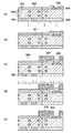
本実施例の光電変換素子100の製造方法について図3により説明する。まず、光電変換部301や周辺回路(不図示)などが形成された半導体基板300の上に層間絶縁膜302、配線303などが形成された部材を準備する。層間絶縁膜302の表面に、パッシベーション層305を形成し、その後、電極パッド304が配置される領域に形成されたパッシベーション層305を選択的にエッチングし、電極パッド304の上部が露出するように開口306を形成する。
A method for manufacturing the
次に図3(b)に示すように、光電変換部301が複数配置されている領域Aの上部の開口308および領域Cの電極パッド304の上部の開口306以外の領域に分散層307を形成する。分散層307は、樹脂などの有機物およびこの有機物に分散した粒子を含む層である。分散層307においては、有機物が分散媒、粒子が分散質である。分散質としての粒子は顔料が好ましい。粒子を含有する分散層307の形成は、粒子が分散された感光性の液体有機材料をパッシベーション層305に塗布する。その後、乾燥処理などを経て有機材料の塗膜である有機材料膜を形成する。この有機材料膜をパターン露光し、現像処理することにより、フォトリソグラフィ技術によりパターニングして形成する。このパターニングでは、有機材料膜の電極パッド304の上に位置する部分を除去することで、開口306を形成する。また、有機材料膜の光電変換部301の上に位置する部分を除去することで、開口308を形成する。以上のようにして光電変換部301上の開口308および電極パッド304上の開口306以外の部分に分散層307を形成する。分散層307は上述した液体有機材料が硬化した有機物と、この有機物に分散した粒子を含む。
Next, as shown in FIG. 3B, a
有機材料には例えばアクリル系樹脂を使用できる。また、顔料には、有機顔料でも無機顔料でも使用できる。有色の材料、特に青色や黒色の顔料が反射光を吸収するのに有利である。分散層307において分散している粒子は、顔料に限らず、シリカ、チタニア又はアルミナなどでもよい。次に、図3(c)に示すように、ドライエッチングを行い、パターニングされた、粒子を含有する分散層307の上部表面の粗面化処理を行う。エッチング条件は以下とした。
・圧力:15 mTorr
・高周波電力:500 W
・エッチングガス:CF4/O2=100/10 sccm
・時間:60sec
エッチング条件は、圧力が1〜100mTorrの範囲内、高周波電力が100〜1000Wの範囲内、エッチングガスとしてCF4及びO2を、流量をそれぞれ0〜500sccm及び1〜500sccmの範囲内で用いればよい。
As the organic material, for example, an acrylic resin can be used. As the pigment, either an organic pigment or an inorganic pigment can be used. Colored materials, especially blue and black pigments, are advantageous for absorbing reflected light. The particles dispersed in the
・ Pressure: 15 mTorr
・ High frequency power: 500 W
Etching gas: CF 4 / O 2 = 100/10 sccm
・ Time: 60 sec
Etching conditions are such that the pressure is in the range of 1 to 100 mTorr, the high-frequency power is in the range of 100 to 1000 W, the etching gas is CF 4 and O 2 , and the flow rates are in the range of 0 to 500 sccm and 1 to 500 sccm, respectively. .
光電変換部301上の開口308および該電極パッド上の開口306の領域は、それぞれパッシベーション層305及び電極パッド304によりエッチングが阻止される。しかし、図3(d)に示すように、粒子を含有する有機物からなる分散層307の上部表面は粗面化されて凸凹な粗面310が形成される。これにより、粗面310を有する反射防止層309が形成される。SIIナノテクノロジー(株)社製の原子間力顕微鏡L−traceIIにて粗面化された反射防止層309の表面粗さを測定したところRMS(二乗平均平方根)で60.7nmであった。なお、粗面化処理前の分散層307の表面粗さは43.5nmであった。上記のようにして、粒子と有機物による粗面化された粗面310を表面の一部に有する光電変換素子を作製した。界面での光の反射を低減するのに適した反射防止層309の凸凹な粗面310の表面粗さはRMSで50nm以上がよい。RMSで50nm未満の表面粗さを有する分散層307に対してこのような粗面化処理を行うことが有用である。このような表面粗さを実現するために有機材料に含有させる粒子の粒径はメジアン径で30〜100nmがよい。粒子を含んだ有機材料を使うことにより、エッチング選択比を高めることができ、凸凹を形成しやすい。例えば、ドライエッチングでは、エッチング選択比の違いによって粒子に比べて有機物がエッチングされやすい。そのため、分散した粒子が分散層307の表面に露出する。粒子の持つ形状によって凸凹が強調されることで、反射防止に十分な凸凹が得られる。そのため、反射防止層309の粗面310は、粒子と有機物との双方が露出した状態で構成されている形態が望ましいと云える。
Etching of the regions of the
本実施例では反射防止層309を形成するための材料に粒子を分散して含有する有機材料を用いることによりエッチングによる粗面化処理の工程を短縮し、反射防止効果を向上させた。本実施例では光電変換素子の最上面に粗面を形成したが、粗面は平坦化層や透明材料で覆われていてもよい。顔料を含む有機材料には、カラーフィルタに使用する材料を使うことができる。この場合、カラーフィルタを形成するときに、反射防止層を形成する領域にもカラーフィルタと同じ材質の層を形成し、反射防止層とする領域の表面を選択的にエッチングして粗面化して反射防止層を形成してもよい。この場合、反射防止層の上にマイクロレンズや透明層を配置してもよい。
In this embodiment, the use of an organic material in which particles are dispersed in the material for forming the
[実施例2]
次に、実施例2について図4により説明する。図4は、図1のA−A’の線に対応した光電変換素子100の一部の断面を示す。実施例1と同じ構成には同じ参照番号を付し、重複する説明は省略する。実施例1と同じく、図4(a)に示すように、フォトダイオード301や周辺回路(不図示)などが形成された半導体基板300に層間絶縁膜302、配線303などが形成された部材を準備する。次に、部材にパッシベーション層305を形成し、その後、開口306を形成する。
[Example 2]
Next, Example 2 will be described with reference to FIG. FIG. 4 shows a partial cross section of the
次に図4(b)に示すように、パッシベーション層305の上部に平坦化層311を形成する。本実施例の平坦化層311は、アクリル系の樹脂を用い、スピンコートにて塗布後、ベークして形成した。この時点で平坦化層311の表面粗さはRMSで13.5nmであった。
Next, as shown in FIG. 4B, a
次に図4(c)に示すように、光電変換部301が配置されている領域Aの上部の開口308と領域Cの電極パッド304の上部の開口306以外の領域に顔料などの粒子を含む分散層307を形成した。具体的には、実施例1と同様に有機材料を塗布、露光、現像を行いパターニングし、光電変換部上の開口308および電極パッド上の開口306以外の部分に分散層307を形成した。
Next, as shown in FIG. 4C, particles such as pigment are included in a region other than the
次に図4(d)に示すように、ドライエッチングを行った。顔料を含有する分散層307の表面の粗面化処理がエッチングにより行われる。粗面化処理と同時に、分散層307をマスクとして、該開口308、309の底部に露出している下地の平坦化層311をエッチングにより除去した。なおエッチング条件は以下とした。
・圧力:15 mTorr
・高周波電力:500 W
・エッチングガス:O2/N2/Ar=80/20/100 sccm
・時間:60sec
エッチング条件は、圧力が1〜100mTorrの範囲内、高周波電力が100〜1000Wの範囲内、エッチングガスとしてO2、N2及びArを、流量をそれぞれ0〜100sccm、1〜50sccm及び1〜200sccmの範囲内であればよい。
Next, as shown in FIG. 4D, dry etching was performed. The surface of the
・ Pressure: 15 mTorr
・ High frequency power: 500 W
Etching gas: O 2 / N 2 / Ar = 80/20/100 sccm
・ Time: 60 sec
The etching conditions are as follows: the pressure is in the range of 1 to 100 mTorr, the high frequency power is in the range of 100 to 1000 W, the etching gases are O 2 , N 2 and Ar, and the flow rates are 0 to 100 sccm, 1 to 50 sccm and 1 to 200 sccm, respectively. It may be within the range.
図4の(e)に示すように、粗面化処理後の顔料を含有する有機材料の上部表面は粗面化されて粗面310が形成される。SIIナノテクノロジー(株)社製の原子間力顕微鏡L−traceIIにて粗面化された分散層307の表面粗さを測定したところRMSで65.2nmとなった。上記のようにして、顔料を含んだ有機材料による粗面化された表面を一部に有する光電変換素子を作製した。
As shown in FIG. 4E, the upper surface of the organic material containing the pigment after the roughening treatment is roughened to form a
本実施例でエッチングに使用したガス種は実施例1と異なる。本実施例では平坦化層が形成されている。顔料を含有する有機材料の表面の粗面化処理と同時に、電極パッド上の平坦化層をエッチング除去する場合、電極パッド上に平坦化層が残らないように十分オーバーエッチングを行う必要がある。実施例1のようにCF系のガスが混合していると電極パッドあるいは光電変換部上のパッシベーション層がエッチングされてしまう可能性を抑制するためである。 The gas species used for etching in this example is different from that in Example 1. In this embodiment, a planarizing layer is formed. When the planarizing layer on the electrode pad is etched away simultaneously with the roughening treatment of the surface of the organic material containing the pigment, it is necessary to perform over-etching sufficiently so that the planarizing layer does not remain on the electrode pad. This is to suppress the possibility that the passivation layer on the electrode pad or the photoelectric conversion portion is etched when the CF gas is mixed as in the first embodiment.
本実施例では反射防止層に光を吸収する粒子を含有する有機材料を用い、更に、分散層の上部表面をエッチングにより粗面化処理を行い、該上部表面に微小な凸凹を形成することにより反射防止効果を向上させた。さらに、本実施例ではパッシベーション層上に平坦化層を配置している。パッシベーション層下部の配線層等により段差が大きい場合は、平坦化層がないと顔料を含有する有機材料をスピン塗布する際、ストリエーションが発生する可能性がある。そのために反射防止の効果にムラが発生し反射防止効果を低減させる可能性がある。また、パッシベーション層と顔料を含有する有機材料との密着性が低い場合、膜剥れを発生させる可能性がある。パッシベーション層上に平坦化層を配置することにより上記懸念は抑制できる。 In this embodiment, an organic material containing light-absorbing particles is used for the antireflection layer, and the upper surface of the dispersion layer is roughened by etching to form minute irregularities on the upper surface. Improved antireflection effect. Further, in this embodiment, a planarizing layer is disposed on the passivation layer. When the level difference is large due to the wiring layer or the like below the passivation layer, striation may occur when an organic material containing a pigment is spin-coated without a planarizing layer. For this reason, unevenness occurs in the antireflection effect, which may reduce the antireflection effect. Further, when the adhesion between the passivation layer and the organic material containing the pigment is low, film peeling may occur. The concern can be suppressed by disposing a planarizing layer on the passivation layer.
更に、平坦化層をエッチング除去する際、粒子を含有する有機材料は平坦化層に対してエッチングの選択比が高いため、エッチングが容易である。 Furthermore, when the planarizing layer is removed by etching, the organic material containing particles has a high etching selectivity with respect to the planarizing layer, so that the etching is easy.
300:光電変換素子、301:フォトダイオード、302:層間絶縁膜、303:配線、304:電極パッド、305:パッシベーション層、306:開口、307:分散層、308:開口、309:反射防止層、310:粗面 300: photoelectric conversion element, 301: photodiode, 302: interlayer insulating film, 303: wiring, 304: electrode pad, 305: passivation layer, 306: opening, 307: dispersion layer, 308: opening, 309: antireflection layer, 310: Rough surface
Claims (19)
前記第1層の上に、前記光電変換部および前記周辺回路部を覆うように、有機物および前記有機物中に分散した粒子を含む膜を形成する工程と、
前記膜のうち前記光電変換部の上方に位置する部分を少なくとも除去することによって、前記膜から第2層を形成する工程と、
前記第2層を形成した後に、前記第1層をエッチング阻止層としたドライエッチングにより前記第2層の表面を粗面化する工程と、を含むことを特徴とする光電変換素子の製造方法。 On a member having a photoelectric conversion portion and the peripheral circuit portion, and forming a first layer to cover at least a part of the peripheral circuit portion and the photoelectric conversion unit,
Forming a film containing an organic substance and particles dispersed in the organic substance on the first layer so as to cover the photoelectric conversion part and the peripheral circuit part ;
Forming a second layer from the film by removing at least a portion of the film located above the photoelectric conversion unit;
After forming the second layer, producing how the photoelectric conversion device characterized by comprising a step of roughening the surface of the second layer by dry etching the first layer as an etching blocking layer .
前記半導体基板の前記光電変換部と前記周辺回路部の少なくとも一部との上に設けられた第1層と、
前記第1層の上に設けられており、有機物および前記有機物に分散した粒子を含み、表面粗さがRMS50nm以上である第2層と、を備え、
前記第1層は、前記周辺回路部に設けられた電極パッドの上方に位置する部分に開口を有し、
前記第2層は、前記電極パッドの上方に位置する部分と前記光電変換部の上方に位置する部分とに開口を有することを特徴とする光電変換素子。 A semiconductor substrate having a photoelectric conversion part and a peripheral circuit part ;
A first layer provided on the photoelectric conversion unit and at least a part of the peripheral circuit unit of the semiconductor substrate;
Provided on the first layer includes particles dispersed organic matter and the organic material comprises a second layer surface roughness is more than RMS50nm, a,
The first layer has an opening in a portion located above the electrode pad provided in the peripheral circuit portion,
The second layer has an opening in a portion located above the electrode pad and a portion located above the photoelectric conversion unit .
Priority Applications (2)
| Application Number | Priority Date | Filing Date | Title |
|---|---|---|---|
| JP2014086800A JP6310312B2 (en) | 2014-04-18 | 2014-04-18 | Photoelectric conversion element and manufacturing method thereof |
| US14/680,291 US9502460B2 (en) | 2014-04-18 | 2015-04-07 | Photoelectric conversion element and method of manufacturing the same |
Applications Claiming Priority (1)
| Application Number | Priority Date | Filing Date | Title |
|---|---|---|---|
| JP2014086800A JP6310312B2 (en) | 2014-04-18 | 2014-04-18 | Photoelectric conversion element and manufacturing method thereof |
Publications (3)
| Publication Number | Publication Date |
|---|---|
| JP2015207638A JP2015207638A (en) | 2015-11-19 |
| JP2015207638A5 JP2015207638A5 (en) | 2017-05-25 |
| JP6310312B2 true JP6310312B2 (en) | 2018-04-11 |
Family
ID=54322678
Family Applications (1)
| Application Number | Title | Priority Date | Filing Date |
|---|---|---|---|
| JP2014086800A Expired - Fee Related JP6310312B2 (en) | 2014-04-18 | 2014-04-18 | Photoelectric conversion element and manufacturing method thereof |
Country Status (2)
| Country | Link |
|---|---|
| US (1) | US9502460B2 (en) |
| JP (1) | JP6310312B2 (en) |
Families Citing this family (6)
| Publication number | Priority date | Publication date | Assignee | Title |
|---|---|---|---|---|
| JP6168915B2 (en) * | 2013-08-22 | 2017-07-26 | キヤノン株式会社 | Manufacturing method of semiconductor device |
| CN111712921A (en) * | 2017-12-12 | 2020-09-25 | 拉芳德利责任有限公司 | Semiconductor optical sensor for visible and ultraviolet light detection and corresponding manufacturing process |
| KR102633533B1 (en) * | 2018-11-09 | 2024-02-06 | 주식회사 엘지화학 | Method for plasma etching process using faraday box |
| US11661332B2 (en) * | 2019-02-20 | 2023-05-30 | Invensense, Inc. | Stiction reduction system and method thereof |
| TWI820308B (en) * | 2019-03-21 | 2023-11-01 | 美商應用材料股份有限公司 | Monitoring of polishing pad texture in chemical mechanical polishing |
| JP2021150473A (en) * | 2020-03-19 | 2021-09-27 | ソニーセミコンダクタソリューションズ株式会社 | Solid-state imaging device and electronic apparatus |
Family Cites Families (20)
| Publication number | Priority date | Publication date | Assignee | Title |
|---|---|---|---|---|
| JPH01164073A (en) * | 1987-09-11 | 1989-06-28 | Canon Inc | Optoelectric conversion device |
| JP2774006B2 (en) * | 1991-12-25 | 1998-07-09 | 三菱電機株式会社 | Semiconductor light receiving device and method of manufacturing the same |
| JPH06302845A (en) * | 1993-04-19 | 1994-10-28 | Olympus Optical Co Ltd | Formation of antireflection film |
| JP3921952B2 (en) | 2001-02-28 | 2007-05-30 | 凸版印刷株式会社 | Image sensor and manufacturing method thereof |
| TWI234885B (en) * | 2002-03-26 | 2005-06-21 | Fujikura Ltd | Electroconductive glass and photovoltaic cell using the same |
| JP4587772B2 (en) * | 2004-10-22 | 2010-11-24 | イビデン株式会社 | Multilayer printed wiring board |
| US7687326B2 (en) * | 2004-12-17 | 2010-03-30 | Semiconductor Energy Laboratory Co., Ltd. | Semiconductor device and manufacturing method thereof |
| WO2006085634A1 (en) * | 2005-02-10 | 2006-08-17 | Semiconductor Energy Laboratory Co., Ltd. | Semiconductor device and manufacturing method of the same |
| JP2007053153A (en) * | 2005-08-16 | 2007-03-01 | Toppan Printing Co Ltd | Solid imaging element and its manufacturing method |
| JP2009168872A (en) * | 2008-01-11 | 2009-07-30 | Sony Corp | Method for manufacturing lens and solid state imaging apparatus |
| JP2009283902A (en) * | 2008-04-25 | 2009-12-03 | Panasonic Corp | Optical device and electronic apparatus including the same |
| JP2010085754A (en) * | 2008-09-30 | 2010-04-15 | Fujifilm Corp | Method of manufacturing color filter and solid-state imaging device |
| JP2010134228A (en) * | 2008-12-05 | 2010-06-17 | Fujifilm Corp | Method for producing color filter and solid-state imaging apparatus |
| JP5446387B2 (en) * | 2009-03-31 | 2014-03-19 | ソニー株式会社 | Method for manufacturing antireflection structure and method for manufacturing solid-state imaging device |
| JP2010272612A (en) * | 2009-05-20 | 2010-12-02 | Sony Corp | Solid-state imaging device, method of manufacturing the same, and imaging device |
| JP5657337B2 (en) * | 2009-10-19 | 2015-01-21 | 富士フイルム株式会社 | Titanium black dispersion for wafer level lens, photosensitive resin composition containing the same, and wafer level lens |
| US8268058B2 (en) * | 2009-11-16 | 2012-09-18 | Fu-Chi Wu | High-performance labyrinth type air treatment apparatus |
| JP2012204402A (en) * | 2011-03-23 | 2012-10-22 | Toshiba Corp | Solid-state imaging device and method of manufacturing the same |
| JP2012203083A (en) * | 2011-03-24 | 2012-10-22 | Sumitomo Osaka Cement Co Ltd | Visible and near-infrared light shielding black film, substrate with visible and near-infrared light shielding black film, and solid-state imaging device |
| JP5681597B2 (en) * | 2011-09-20 | 2015-03-11 | 富士フイルム株式会社 | Manufacturing method of solid-state imaging device |
-
2014
- 2014-04-18 JP JP2014086800A patent/JP6310312B2/en not_active Expired - Fee Related
-
2015
- 2015-04-07 US US14/680,291 patent/US9502460B2/en active Active
Also Published As
| Publication number | Publication date |
|---|---|
| US9502460B2 (en) | 2016-11-22 |
| US20150303226A1 (en) | 2015-10-22 |
| JP2015207638A (en) | 2015-11-19 |
Similar Documents
| Publication | Publication Date | Title |
|---|---|---|
| JP6310312B2 (en) | Photoelectric conversion element and manufacturing method thereof | |
| TWI278991B (en) | Solid image-pickup device and method of manufacturing the same | |
| JP6298394B2 (en) | Double lens structure and manufacturing method thereof | |
| US7898049B2 (en) | Touching microlens structure for a pixel sensor and method of fabrication | |
| JP2007053153A (en) | Solid imaging element and its manufacturing method | |
| US10178286B2 (en) | Method for forming color filter array, method for manufacturing imaging apparatus, and imaging apparatus | |
| JP2011171328A (en) | Solid-state image pickup element and method of manufacturing the same | |
| JP2013012518A (en) | Solid state imaging device | |
| JP4984400B2 (en) | Solid-state imaging device and manufacturing method thereof | |
| TW202236696A (en) | Spectrum chip and preparation method therefor, and spectrum analysis device | |
| TWI222178B (en) | Manufacturing method of image sensor device | |
| TW201944585A (en) | Optical sensors and methods for forming the same | |
| JP5836637B2 (en) | PATTERN FORMING METHOD, SOLID-STATE IMAGING DEVICE, AND SOLID-STATE IMAGING DEVICE MANUFACTURING METHOD | |
| JP5564751B2 (en) | Manufacturing method of image sensor | |
| US20200075651A1 (en) | Double-layer color filter and method for forming the same | |
| JP2006190944A (en) | Image sensor die | |
| JP2000307090A (en) | Solid-state image sensing device microlens array, solid- state image sensing device provided with it, and method of manufacturing them | |
| JPH01270362A (en) | Solid-state image sensing device and manufacture thereof | |
| JP6499741B2 (en) | Optical sensor and manufacturing method thereof | |
| JP4935118B2 (en) | Image sensor manufacturing method and image sensor | |
| JP2009152315A (en) | Image sensor and its manufacturing method | |
| JPH06302794A (en) | Manufacture of solid-state image sensing element | |
| JP2010054923A (en) | Color imaging device and manufacturing method of same | |
| JP2016219703A (en) | Solid-state imaging element and method for manufacturing solid-state imaging element | |
| JP2014103299A (en) | Solid state image sensor |
Legal Events
| Date | Code | Title | Description |
|---|---|---|---|
| A521 | Request for written amendment filed |
Free format text: JAPANESE INTERMEDIATE CODE: A523 Effective date: 20170404 |
|
| A621 | Written request for application examination |
Free format text: JAPANESE INTERMEDIATE CODE: A621 Effective date: 20170404 |
|
| A977 | Report on retrieval |
Free format text: JAPANESE INTERMEDIATE CODE: A971007 Effective date: 20171109 |
|
| A131 | Notification of reasons for refusal |
Free format text: JAPANESE INTERMEDIATE CODE: A131 Effective date: 20171117 |
|
| A521 | Request for written amendment filed |
Free format text: JAPANESE INTERMEDIATE CODE: A523 Effective date: 20180116 |
|
| TRDD | Decision of grant or rejection written | ||
| A01 | Written decision to grant a patent or to grant a registration (utility model) |
Free format text: JAPANESE INTERMEDIATE CODE: A01 Effective date: 20180216 |
|
| A61 | First payment of annual fees (during grant procedure) |
Free format text: JAPANESE INTERMEDIATE CODE: A61 Effective date: 20180316 |
|
| R151 | Written notification of patent or utility model registration |
Ref document number: 6310312 Country of ref document: JP Free format text: JAPANESE INTERMEDIATE CODE: R151 |
|
| LAPS | Cancellation because of no payment of annual fees |