JP2012204402A - Solid-state imaging device and method of manufacturing the same - Google Patents

Solid-state imaging device and method of manufacturing the same Download PDF

Info

Publication number
JP2012204402A
JP2012204402A JP2011064929A JP2011064929A JP2012204402A JP 2012204402 A JP2012204402 A JP 2012204402A JP 2011064929 A JP2011064929 A JP 2011064929A JP 2011064929 A JP2011064929 A JP 2011064929A JP 2012204402 A JP2012204402 A JP 2012204402A
Authority
JP
Japan
Prior art keywords
black reference
film
light
region
semiconductor substrate
Prior art date
Legal status (The legal status is an assumption and is not a legal conclusion. Google has not performed a legal analysis and makes no representation as to the accuracy of the status listed.)
Withdrawn
Application number
JP2011064929A
Other languages
Japanese (ja)
Inventor
Hiromichi Seki
弘道 関
Current Assignee (The listed assignees may be inaccurate. Google has not performed a legal analysis and makes no representation or warranty as to the accuracy of the list.)
Toshiba Corp
Original Assignee
Toshiba Corp
Priority date (The priority date is an assumption and is not a legal conclusion. Google has not performed a legal analysis and makes no representation as to the accuracy of the date listed.)
Filing date
Publication date
Application filed by Toshiba Corp filed Critical Toshiba Corp
Priority to JP2011064929A priority Critical patent/JP2012204402A/en
Publication of JP2012204402A publication Critical patent/JP2012204402A/en
Withdrawn legal-status Critical Current

Links

Images

Abstract

PROBLEM TO BE SOLVED: To improve the image quality of a solid-state imaging device.SOLUTION: A solid-state imaging device comprises: unit cells that are provided in an imaging region 21 of a semiconductor substrate 10 and include at least one photoelectric conversion element 30; black reference cells that are provided in a black reference region 29 of the semiconductor substrate 10 and include at least one photoelectric conversion element 40; lenses 60 that are provided above the unit cells via an insulating film 71 on the semiconductor substrate 10; and a first light-shielding film 61 that is provided above the black reference cells via the insulating film 71 and has a concave-convex portion 62 on its surface.

Description

本発明の実施形態は、固体撮像装置及びその製造方法に関する。   Embodiments described herein relate generally to a solid-state imaging device and a method for manufacturing the same.

CCDイメージセンサやCOMSイメージセンサなどの固体撮像装置は、デジタルスチルカメラ、ビデオカメラ、或いは、監視カメラ等、多様な用途で使われている。   Solid-state imaging devices such as CCD image sensors and COMS image sensors are used in various applications such as digital still cameras, video cameras, and surveillance cameras.

イメージセンサの光電変換部には、例えば、フォトダイオードが用いられている。フォトダイオードに入射された光が、光電変換され、画像(被写体)に対応した電気信号が得られる。   For example, a photodiode is used in the photoelectric conversion unit of the image sensor. Light incident on the photodiode is photoelectrically converted to obtain an electrical signal corresponding to the image (subject).

イメージセンサは、フォトダイオードが設けられる画素アレイ内に、被写体に対応する入射光を取り込む撮像領域と、入射光を取り込まないように遮光された遮光領域とを含んでいる。   The image sensor includes, in a pixel array provided with a photodiode, an imaging region that captures incident light corresponding to a subject, and a light shielding region that is shielded so as not to capture incident light.

遮光領域は、イメージセンサの特性の基準となる黒を形成するために設けられ、黒基準領域ともよばれる。遮光領域は、画素アレイ内のフォトダイオード上方に、金属膜を設け、フォトダイオードに対する入射光を、金属膜によって遮ることによって、形成されている。   The light shielding area is provided to form black which is a reference for the characteristics of the image sensor, and is also referred to as a black reference area. The light shielding region is formed by providing a metal film above the photodiode in the pixel array and blocking incident light on the photodiode with the metal film.

特開2007−53153号公報JP 2007-53153 A

形成される画像の画質を向上する技術を提案する。   A technique for improving the image quality of the formed image is proposed.

本実施形態の固体撮像装置は、半導体基板の撮像領域内に設けられ、少なくとも1つの光電変換素子を含む単位セルと、前記半導体基板の黒基準領域内に設けられ、少なくとも1つの光電変換素子を含む黒基準セルと、前記半導体基板上の絶縁膜を介して、前記単位セルの上方に設けられるレンズと、前記絶縁膜上を介して、前記黒基準セルの上方に設けられ、表面に凸凹部を有する第1の遮光膜と、を含む。   The solid-state imaging device of the present embodiment is provided in an imaging region of a semiconductor substrate, and includes a unit cell including at least one photoelectric conversion element, and a black reference region of the semiconductor substrate, and includes at least one photoelectric conversion element. Including a black reference cell, a lens provided above the unit cell via an insulating film on the semiconductor substrate, and provided above the black reference cell via the insulating film, and having a concave and convex surface And a first light-shielding film.

固体撮像装置の構造を示す平面図。The top view which shows the structure of a solid-state imaging device. 画素アレイの構成を示す等価回路図。The equivalent circuit diagram which shows the structure of a pixel array. 第1の実施形態の固体撮像装置の構造を示す断面図。1 is a cross-sectional view illustrating a structure of a solid-state imaging device according to a first embodiment. 第1の実施形態の固体撮像装置の製造方法の一工程を示す断面図。Sectional drawing which shows 1 process of the manufacturing method of the solid-state imaging device of 1st Embodiment. 第1の実施形態の固体撮像装置の製造方法の一工程を示す断面図。Sectional drawing which shows 1 process of the manufacturing method of the solid-state imaging device of 1st Embodiment. 第1の実施形態の固体撮像装置の製造方法の一工程を示す断面図。Sectional drawing which shows 1 process of the manufacturing method of the solid-state imaging device of 1st Embodiment. 第1の実施形態の固体撮像装置の製造方法の一工程を示す断面図。Sectional drawing which shows 1 process of the manufacturing method of the solid-state imaging device of 1st Embodiment. 第2の実施形態の固体撮像装置の構造を示す断面図。Sectional drawing which shows the structure of the solid-state imaging device of 2nd Embodiment. 実施形態の固体撮像装置の変形例を示す断面図。Sectional drawing which shows the modification of the solid-state imaging device of embodiment. 実施形態の固体撮像装置の変形例を示す断面図。Sectional drawing which shows the modification of the solid-state imaging device of embodiment.

[実施形態]
以下、図面を参照しながら、本実施形態について詳細に説明する。以下の説明において、同一の機能及び構成を有する要素については、同一符号を付し、重複する説明は必要に応じて行う。
[Embodiment]
Hereinafter, this embodiment will be described in detail with reference to the drawings. In the following description, elements having the same function and configuration are denoted by the same reference numerals, and redundant description will be given as necessary.

(1) 第1の実施形態
図1乃至図7を参照して、第1の実施形態に係る固体撮像装置及びその製造方法について説明する。
(1) First embodiment
A solid-state imaging device and a method for manufacturing the same according to the first embodiment will be described with reference to FIGS.

(a) 構造
図1乃至図3を用いて、第1の実施形態に係る固体撮像装置の構造について、説明する。
(A) Structure
The structure of the solid-state imaging device according to the first embodiment will be described with reference to FIGS. 1 to 3.

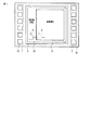
図1は、固体撮像装置(以下、イメージセンサとよぶ)のチップのレイアウト例を示す模式図である。
図1に示されるように、本実施形態のイメージセンサにおいて、画素アレイ2及びそれを制御するための回路(アナログ回路又はロジック回路)が、1つの半導体基板(チップ)10内に設けられている。
FIG. 1 is a schematic diagram illustrating a chip layout example of a solid-state imaging device (hereinafter referred to as an image sensor).
As shown in FIG. 1, in the image sensor of this embodiment, a pixel array 2 and a circuit (analog circuit or logic circuit) for controlling the pixel array 2 are provided in one semiconductor substrate (chip) 10. .

半導体基板10内の画素アレイ2は、画像(被写体)に対応する光を取得するための撮像領域(有効領域ともよばれる)21を含んでいる。
撮像領域21は、有効画素を含む単位セル3を複数個有する。以下では、有効画素を含む単位セル3のことを、単に、単位セルとよぶ。各単位セル3は、少なくとも1つの画素(有効画素、光電変換部)を含んでいる。光電変換部は、マイクロレンズ及びカラーフィルタを介して入射された光を電気信号へ変換する。光電変換部によって、CMOSセンサ或いはCCDセンサが形成される。互いに隣接する単位セル3及び互いに隣接する光電変換部は、素子分離領域によって、分離されている。
The pixel array 2 in the semiconductor substrate 10 includes an imaging region (also referred to as an effective region) 21 for acquiring light corresponding to an image (subject).
The imaging region 21 has a plurality of unit cells 3 including effective pixels. Hereinafter, the unit cell 3 including the effective pixel is simply referred to as a unit cell. Each unit cell 3 includes at least one pixel (effective pixel, photoelectric conversion unit). The photoelectric conversion unit converts light incident through the microlens and the color filter into an electric signal. A CMOS sensor or a CCD sensor is formed by the photoelectric conversion unit. The unit cells 3 adjacent to each other and the photoelectric conversion units adjacent to each other are separated by an element isolation region.

画素アレイ2は、黒基準領域29を含んでいる。黒基準領域29は、光電変換された信号に対する基準電位(暗電圧又はリセット電圧)を形成するために、画素アレイ2内に設けられている。黒基準領域29は、OB(Optical Black)領域、遮光領域、あるいは、無効領域ともよばれる。   The pixel array 2 includes a black reference area 29. The black reference region 29 is provided in the pixel array 2 in order to form a reference potential (dark voltage or reset voltage) for the photoelectrically converted signal. The black reference area 29 is also called an OB (Optical Black) area, a light shielding area, or an invalid area.

黒基準領域29は、画素アレイ2内において、撮像領域21に隣接している。例えば、黒基準領域29は、撮像領域21の周囲を取り囲むように、画素アレイ2内にレイアウトされている。
黒基準領域29は、複数の黒基準画素を含む単位セル4を有している。以下では、黒基準領域29内の黒基準画素を含む単位セル4のことを、単に、黒基準セル4とよぶ。黒基準セル4は、単位セル20と実質的に同じ構造を有し、画素を含んでいる。光の入射を遮る遮光膜が、黒基準セル4上方に、設けられていることによって、黒基準領域29が、形成される。尚、黒基準セル4は、ダミーセルとよばれる場合もある。
The black reference area 29 is adjacent to the imaging area 21 in the pixel array 2. For example, the black reference area 29 is laid out in the pixel array 2 so as to surround the imaging area 21.
The black reference area 29 has a unit cell 4 including a plurality of black reference pixels. Hereinafter, the unit cell 4 including the black reference pixel in the black reference region 29 is simply referred to as the black reference cell 4. The black reference cell 4 has substantially the same structure as the unit cell 20 and includes pixels. A black reference region 29 is formed by providing a light-shielding film that blocks the incidence of light above the black reference cell 4. The black reference cell 4 is sometimes called a dummy cell.

半導体基板10内には、アナログ回路又はロジック回路を配置するための領域(以下、周辺領域)7が設けられている。周辺領域7は、画素アレイ2に隣接するように設けられている。例えば、イメージセンサチップと他の装置とを接続するためのパッド70は、周辺領域7上方に設けられている。パッド70は、半導体基板10上の層間絶縁膜上に設けられている。   In the semiconductor substrate 10, a region (hereinafter referred to as a peripheral region) 7 for arranging an analog circuit or a logic circuit is provided. The peripheral region 7 is provided so as to be adjacent to the pixel array 2. For example, the pad 70 for connecting the image sensor chip and another device is provided above the peripheral region 7. The pad 70 is provided on the interlayer insulating film on the semiconductor substrate 10.

図2は、画素アレイ2及びその近傍の回路の回路構成の一例を示す図である。   FIG. 2 is a diagram illustrating an example of a circuit configuration of the pixel array 2 and a circuit in the vicinity thereof.

図2に示されるように、複数の単位セル20は、画素アレイ2内に、マトリクス状に配置されている。   As shown in FIG. 2, the plurality of unit cells 20 are arranged in a matrix in the pixel array 2.

単位セル20は、光電変換部(フォトダイオード)5及び信号走査回路部を含む。
セル20の信号走査回路部は、例えば、4つの電界効果トランジスタ132,133,134,135によって形成される。各電界効果トランジスタ132,133,134,135は、例えば、nチャネル型MOSトランジスタである。以下では、セル20に含まれる4つの電界効果トランジスタのことを、トランスファゲート(リードトランジスタ)132、アンプトランジスタ133、アドレストランジスタ134及びリセットトランジスタ135とそれぞれよぶ。
The unit cell 20 includes a photoelectric conversion unit (photodiode) 5 and a signal scanning circuit unit.
The signal scanning circuit section of the cell 20 is formed by, for example, four field effect transistors 132, 133, 134, and 135. Each field effect transistor 132, 133, 134, 135 is, for example, an n-channel MOS transistor. Hereinafter, the four field effect transistors included in the cell 20 are referred to as a transfer gate (read transistor) 132, an amplifier transistor 133, an address transistor 134, and a reset transistor 135, respectively.

図2に示される単位セル20において、フォトダイオード30のアノードは接地されている。フォトダイオード30のカソードは、トランスファゲート132の電流経路を介して、信号検出部としてのフローティングディフュージョン(浮遊拡散層)FDに、接続されている。   In the unit cell 20 shown in FIG. 2, the anode of the photodiode 30 is grounded. The cathode of the photodiode 30 is connected to a floating diffusion (floating diffusion layer) FD as a signal detection unit via a current path of the transfer gate 132.

トランスファゲート132は、フォトダイオード30の信号電荷の蓄積及び放出を制御する。トランスファゲート132のゲートは読み出し信号線TRFに接続されている。トランスファゲート132のソースは、フォトダイオード30のカソードに接続され、トランスファゲート132のドレインは、フローティングディフュージョンFDに接続されている。   The transfer gate 132 controls the accumulation and emission of signal charges of the photodiode 30. The gate of the transfer gate 132 is connected to the read signal line TRF. The source of the transfer gate 132 is connected to the cathode of the photodiode 30, and the drain of the transfer gate 132 is connected to the floating diffusion FD.

アンプトランジスタ133は、フローティングディフュージョンFDからの信号を増幅する。アンプトランジスタ133のゲートは、フローティングディフュージョンFDに接続されている。アンプトランジスタ133のドレインは、垂直信号線VSLに接続され、アンプトランジスタ133のソースは、アドレストランジスタ134のドレインに接続されている。アンプトランジスタ133によって増幅された信号は、垂直信号線VSLに出力される。アンプトランジスタ133は、単位セル20内において、ソースフォロワとして機能する。   The amplifier transistor 133 amplifies the signal from the floating diffusion FD. The gate of the amplifier transistor 133 is connected to the floating diffusion FD. The drain of the amplifier transistor 133 is connected to the vertical signal line VSL, and the source of the amplifier transistor 133 is connected to the drain of the address transistor 134. The signal amplified by the amplifier transistor 133 is output to the vertical signal line VSL. The amplifier transistor 133 functions as a source follower in the unit cell 20.

リセットトランジスタ135は、アンプトランジスタ133のゲート電位(フローティングディフュージョンFDの電位)をリセットする。リセットトランジスタ135のゲートは、リセット信号線RSTに接続されている。リセットトランジスタ135のドレインは、フローティングディフュージョンFDに接続され、リセットトランジスタ135のソースは、基準電位が印加される端子124に接続されている。以下では、この端子124のことを、基準電位端子とよぶ。   The reset transistor 135 resets the gate potential of the amplifier transistor 133 (the potential of the floating diffusion FD). The gate of the reset transistor 135 is connected to the reset signal line RST. The drain of the reset transistor 135 is connected to the floating diffusion FD, and the source of the reset transistor 135 is connected to a terminal 124 to which a reference potential is applied. Hereinafter, the terminal 124 is referred to as a reference potential terminal.

アドレストランジスタ134のゲートは、アドレス信号線ADRに接続されている。アドレストランジスタ134のドレインは、アンプトランジスタ133のソースに接続され、アドレストランジスタ134のソースは、基準電位端子124に接続されている。   The gate of the address transistor 134 is connected to the address signal line ADR. The drain of the address transistor 134 is connected to the source of the amplifier transistor 133, and the source of the address transistor 134 is connected to the reference potential terminal 124.

1つの単位セル20が、1つのフォトダイオード30を含む回路構成は、1画素1セル構造とよばれる。これに対して、1つの単位セル20が、2つのフォトダイオードを含む回路構成は、2画素1セル構造とよばれる。2画素1セル構造の場合、2つのフォトダイオードは、それぞれ異なるトランスファゲートを経由して、共通のフローティングディフュージョンFDに接続される。2画素1セル構造において、2つのフォトダイオードは、アンプトランジスタ133、アドレストランジスタ134及びリセットトランジスタ135を共有する。   A circuit configuration in which one unit cell 20 includes one photodiode 30 is called a one-pixel one-cell structure. On the other hand, a circuit configuration in which one unit cell 20 includes two photodiodes is called a two-pixel one-cell structure. In the case of the two-pixel one-cell structure, the two photodiodes are connected to a common floating diffusion FD via different transfer gates. In the 2-pixel 1-cell structure, the two photodiodes share the amplifier transistor 133, the address transistor 134, and the reset transistor 135.

尚、各単位セル20は、アドレストランジスタ134を含まなくともよい。この場合、セル20は、3つのトランジスタ132,133,135を含み、リセットトランジスタ135のドレインが、アンプトランジスタ133のソースに接続された構成となる。また、この場合、アドレス信号線ADRも設けられない。   Each unit cell 20 may not include the address transistor 134. In this case, the cell 20 includes three transistors 132, 133, and 135, and the drain of the reset transistor 135 is connected to the source of the amplifier transistor 133. In this case, the address signal line ADR is not provided.

垂直シフトレジスタ89は、読み出し信号線TRF、アドレス信号線ADR及びリセット信号線RSTに接続されている。垂直シフトレジスタ89は、読み出し信号線TRF、アドレス信号線ADR及びリセット信号線RSTの電位を制御することによって、画素アレイ2内の複数の単位セル20をロウ単位で制御及び選択する。垂直シフトレジスタ89は、各トランジスタ132,134,135のオン及びオフを制御するための制御信号(電圧パルス)を、各信号線TRF,ADR,RSTに出力する。   The vertical shift register 89 is connected to the read signal line TRF, the address signal line ADR, and the reset signal line RST. The vertical shift register 89 controls and selects the plurality of unit cells 20 in the pixel array 2 in units of rows by controlling the potentials of the read signal line TRF, the address signal line ADR, and the reset signal line RST. The vertical shift register 89 outputs a control signal (voltage pulse) for controlling on and off of the transistors 132, 134, and 135 to the signal lines TRF, ADR, and RST.

AD変換回路80は、垂直信号線VSLに接続されている。AD変換回路80は、複数のCDS(Corrected Double Sampling:相関二重サンプリング)ユニット85を含む。1つのCDSユニット85が、1本の垂直信号線VSLに接続されている。AD変換回路80は、垂直信号線VSLに出力された単位セル20からの信号をデジタル値に変換する。AD変換回路80は、CDSユニット85によるCDS処理によって、各単位セル(画素)が含むノイズを除去する。   The AD conversion circuit 80 is connected to the vertical signal line VSL. The AD conversion circuit 80 includes a plurality of CDS (Corrected Double Sampling) units 85. One CDS unit 85 is connected to one vertical signal line VSL. The AD conversion circuit 80 converts the signal from the unit cell 20 output to the vertical signal line VSL into a digital value. The AD conversion circuit 80 removes noise included in each unit cell (pixel) by CDS processing by the CDS unit 85.

負荷トランジスタ121は、垂直信号線VSLに対する電流源として用いられる。負荷トランジスタ121のゲートは選択信号線SFに接続されている。負荷トランジスタ121のドレインは、垂直信号線VSLを介して、アンプトランジスタ133のドレインに接続される。負荷トランジスタ121のソースは、制御信号線DCに接続されている。   The load transistor 121 is used as a current source for the vertical signal line VSL. The gate of the load transistor 121 is connected to the selection signal line SF. The drain of the load transistor 121 is connected to the drain of the amplifier transistor 133 via the vertical signal line VSL. The source of the load transistor 121 is connected to the control signal line DC.

画素アレイ2のセル20からの信号(電荷)の読み出し動作は、次のように実行される。
画素アレイ2の所定のロウが、垂直シフトレジスタ89によって選択され、選択されたロウに属する複数のセル20が活性化される。
選択されたロウに属するアドレストランジスタ134が、垂直シフトレジスタ89からのロウ選択パルスによって、オン状態になる。また、垂直シフトレジスタ89からのリセットパルスによって、リセットトランジスタ135が、オン状態になる。これによって、基準電位端子124からの電位が、フローティングディフュージョンFD及び各トランジスタ133,134,135に印加される。
A signal (charge) reading operation from the cell 20 of the pixel array 2 is performed as follows.
A predetermined row of the pixel array 2 is selected by the vertical shift register 89, and a plurality of cells 20 belonging to the selected row are activated.
The address transistor 134 belonging to the selected row is turned on by a row selection pulse from the vertical shift register 89. Further, the reset transistor 135 is turned on by the reset pulse from the vertical shift register 89. As a result, the potential from the reference potential terminal 124 is applied to the floating diffusion FD and the transistors 133, 134, and 135.

垂直信号線VSLの電位は、ソースフォロワを形成しているアンプトランジスタ133によって、フローティングディフュージョンFDの電位に近い電圧(リセット電圧)に、リセットされる。単位セル20からのリセット電圧は、AD変換回路80に入力される。リセット電圧が垂直信号線VSLに出力された後、リセットトランジスタ135は、オフ状態にされる。   The potential of the vertical signal line VSL is reset to a voltage (reset voltage) close to the potential of the floating diffusion FD by the amplifier transistor 133 forming the source follower. The reset voltage from the unit cell 20 is input to the AD conversion circuit 80. After the reset voltage is output to the vertical signal line VSL, the reset transistor 135 is turned off.

続いて、トランスファゲート132が、垂直シフトレジスタ89からの読み出しパルスによってオン状態になり、フォトダイオード30に蓄積された電荷(信号電荷)が、オン状態のトランスファゲート132を経由して、フローティングディフュージョンFDに放出される。フローティングディフュージョンFDの電位は、フォトダイオードから出力された信号電荷に応じて変調される。変調された電位(信号電圧)が、ソースフォロワを形成しているアンプトランジスタ133によって垂直信号線VSLに出力される。信号電圧は、AD変換回路80に入力される。   Subsequently, the transfer gate 132 is turned on by a read pulse from the vertical shift register 89, and the charge (signal charge) accumulated in the photodiode 30 passes through the transfer gate 132 in the on state, and the floating diffusion FD. To be released. The potential of the floating diffusion FD is modulated according to the signal charge output from the photodiode. The modulated potential (signal voltage) is output to the vertical signal line VSL by the amplifier transistor 133 forming the source follower. The signal voltage is input to the AD conversion circuit 80.

リセット電圧及び信号電圧は、AD変換回路80によって、アナログ値からデジタル値へ順次変換される。これらの電圧値のAD変換とともに、リセット電圧及び信号電圧に対するCDS処理が、CDSユニット85によって実行される。リセット電圧と信号電圧との差分値が画素データDsigとして、後段の回路(例えば、画像処理回路)へ出力される。   The reset voltage and the signal voltage are sequentially converted from an analog value to a digital value by the AD conversion circuit 80. Along with AD conversion of these voltage values, CDS processing for the reset voltage and signal voltage is executed by the CDS unit 85. A difference value between the reset voltage and the signal voltage is output as pixel data Dsig to a subsequent circuit (for example, an image processing circuit).

これによって、所定のロウに属する複数のセル(画素)からの信号の読み出し動作が、完了する。   As a result, the signal reading operation from a plurality of cells (pixels) belonging to a predetermined row is completed.

このような、画素アレイ2に対するロウ単位の読み出し動作が順次繰り返されて、所定の画像が形成される。   Such row-unit readout operations for the pixel array 2 are sequentially repeated to form a predetermined image.

例えば、黒基準領域29からの電位が、リセット電圧を生成するために基準電位として、基準電位端子124から単位セル20に印加されたり、黒基準領域29からの電位に対応するデータ(信号)が、後段の画像処理回路によって画素データDsigと比較されたりする。このように、黒基準領域29の黒基準セルから出力される電位を用いて、画素データDsigによって形成される画像の色調が、判定される。   For example, the potential from the black reference region 29 is applied to the unit cell 20 from the reference potential terminal 124 as a reference potential for generating a reset voltage, or data (signal) corresponding to the potential from the black reference region 29 is received. The image data is compared with the pixel data Dsig by the subsequent image processing circuit. Thus, the color tone of the image formed by the pixel data Dsig is determined using the potential output from the black reference cell in the black reference region 29.

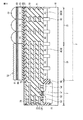
図3は、本実施形態のイメージセンサの画素アレイ2の断面構造を示している。
上述のように、単位セル3は、光電変換部として、少なくとも1つのフォトダイオード30(PD)を含む。フォトダイオード30において、入射光の光量に応じて、フォトダイオード内部に電荷が発生し、フォトダイオード30の端子間に電位差が生じる。フォトダイオード30は発生した電荷を蓄積できる。
FIG. 3 shows a cross-sectional structure of the pixel array 2 of the image sensor of this embodiment.
As described above, the unit cell 3 includes at least one photodiode 30 (PD) as a photoelectric conversion unit. In the photodiode 30, charges are generated inside the photodiode according to the amount of incident light, and a potential difference is generated between the terminals of the photodiode 30. The photodiode 30 can accumulate the generated charges.

画素アレイ2の撮像領域21内において、単位セル3のフォトダイオード30は、半導体基板10内に形成されている。フォトダイオード30は、半導体基板10内に形成された少なくとも1つの不純物層(拡散層)30を含んでいる。   In the imaging region 21 of the pixel array 2, the photodiode 30 of the unit cell 3 is formed in the semiconductor substrate 10. The photodiode 30 includes at least one impurity layer (diffusion layer) 30 formed in the semiconductor substrate 10.

例えば、半導体基板10が、P型の導電型を有する場合、不純物層30は、N型の導電型を有する。尚、フォトダイオードPDの特性(例えば、感度)を向上させるために、フォトダイオード30は、不純物濃度の異なる複数のN型及びP型不純物層を含んでいてもよい。   For example, when the semiconductor substrate 10 has a P-type conductivity type, the impurity layer 30 has an N-type conductivity type. In order to improve the characteristics (for example, sensitivity) of the photodiode PD, the photodiode 30 may include a plurality of N-type and P-type impurity layers having different impurity concentrations.

複数のフォトダイオードPDは、半導体基板10内に設けられた素子分離層90によって、互いに電気的に分離されている。素子分離層90は、例えば、不純物層であってもよいし、STI構造の絶縁膜でもよい。   The plurality of photodiodes PD are electrically isolated from each other by an element isolation layer 90 provided in the semiconductor substrate 10. The element isolation layer 90 may be, for example, an impurity layer or an insulating film having an STI structure.

尚、図3において、素子分離層90に囲まれた領域内において、図示の簡略化のため、フォトダイオード30のみが図示されているが、同じ領域内に、単位セルを構成するトランジスタ132,133,134,135やフローティングディフュージョン(浮遊拡散層)FDが設けられている。   In FIG. 3, only the photodiode 30 is shown in the region surrounded by the element isolation layer 90 for simplification of illustration, but the transistors 132 and 133 constituting the unit cell are shown in the same region. , 134, 135 and a floating diffusion (floating diffusion layer) FD are provided.

黒基準領域29の黒基準セル4は、撮像領域21内の単位セル3と実質的に同じ構造を有する。黒基準セル4は、少なくとも1つのフォトダイオード40を含む。単位セル3及び黒基準セル4内のフォトダイオード30,40を区別するために、黒基準セル4内のフォトダイオード40のことを、ダミーダイオードとよぶ。   The black reference cell 4 in the black reference region 29 has substantially the same structure as the unit cell 3 in the imaging region 21. The black reference cell 4 includes at least one photodiode 40. In order to distinguish the photodiodes 30 and 40 in the unit cell 3 and the black reference cell 4, the photodiode 40 in the black reference cell 4 is called a dummy diode.

ダミーダイオード40は、フォトダイオード30と実質的に同じ構造を有し、半導体基板10内に形成された少なくとも1つの不純物層(例えば、N型不純物層)40によって形成される。ダミーダイオード40は、後述の遮光膜によって、ほとんど光が照射されない。ダミーダイオード40は、基準電位としての暗電圧(暗電流)を、生成及び出力する。ダミーダイオード40から出力される電圧に基づいて、リセット電圧が生成される。   The dummy diode 40 has substantially the same structure as the photodiode 30 and is formed by at least one impurity layer (for example, an N-type impurity layer) 40 formed in the semiconductor substrate 10. The dummy diode 40 is hardly irradiated with light by a light shielding film described later. The dummy diode 40 generates and outputs a dark voltage (dark current) as a reference potential. A reset voltage is generated based on the voltage output from the dummy diode 40.

周辺領域7内において、電界効果トランジスタ(例えば、MOSトランジスタ)Trは、半導体基板10内のウェル領域15内に設けられている。ウェル領域15内に、2つの拡散層(不純物層)53が設けられている。これらの2つの拡散層53は、トランジスタTrのソース/ドレインとして、機能する。2つの拡散層53間のウェル領域(チャネル領域)表面に、ゲート絶縁膜52を介して、ゲート電極51が設けられる。   In the peripheral region 7, a field effect transistor (for example, a MOS transistor) Tr is provided in the well region 15 in the semiconductor substrate 10. Two diffusion layers (impurity layers) 53 are provided in the well region 15. These two diffusion layers 53 function as the source / drain of the transistor Tr. A gate electrode 51 is provided on the surface of the well region (channel region) between the two diffusion layers 53 via the gate insulating film 52.

電界効果トランジスタTrが、Pチャネル型であるかNチャネル型であるかは、そのトランジスタTrが設けられるウェル領域15の導電型及びソース/ドレインとなる拡散層73の導電型によって、決まる。   Whether the field effect transistor Tr is a P-channel type or an N-channel type depends on the conductivity type of the well region 15 in which the transistor Tr is provided and the conductivity type of the diffusion layer 73 serving as the source / drain.

尚、図示の簡単化のために、周辺領域7内に形成される素子として、電界効果トランジスタTrのみが図示されているが、周辺領域7内に、抵抗素子、容量素子、ダイオード又はバイポーラトランジスタなどが、設けられている。   For simplification of illustration, only the field effect transistor Tr is shown as an element formed in the peripheral region 7. However, in the peripheral region 7, a resistor element, a capacitive element, a diode, a bipolar transistor, etc. Is provided.

半導体基板10上に、層間絶縁膜71が設けられている。層間絶縁膜71は、半導体基板10内に形成された素子を、覆っている。層間絶縁膜71を挟んで、画素アレイ2の上方に、カラーフィルタ65及びマイクロレンズ60が設けられている。   An interlayer insulating film 71 is provided on the semiconductor substrate 10. The interlayer insulating film 71 covers elements formed in the semiconductor substrate 10. A color filter 65 and a micro lens 60 are provided above the pixel array 2 with the interlayer insulating film 71 interposed therebetween.

層間絶縁膜71内に、複数の金属膜72,73,75が、設けられている。層間絶縁膜71及び金属膜72,73,75は、多層配線技術によって形成され、所定の配線レベル(基板表面からの高さ)内にそれぞれ設けられている。例えば、層間絶縁膜71は、酸化シリコンを用いて、形成される。金属膜72,73,75は、アルミニウム(Al)或いは銅(Cu)を用いて、形成される。   A plurality of metal films 72, 73, and 75 are provided in the interlayer insulating film 71. The interlayer insulating film 71 and the metal films 72, 73, and 75 are formed by a multilayer wiring technique and are provided within a predetermined wiring level (height from the substrate surface). For example, the interlayer insulating film 71 is formed using silicon oxide. The metal films 72, 73, and 75 are formed using aluminum (Al) or copper (Cu).

撮像領域21内の金属膜72は、マイクロレンズ60及びカラーフィルタ65を透過した光が、マイクロレンズ60及びカラーフィルタ65に対応する画素30のみに入射されるように、隣接する画素間における光の漏れを防止するための遮光膜72として用いられる。   The metal film 72 in the imaging region 21 is configured to transmit light between adjacent pixels so that light transmitted through the microlens 60 and the color filter 65 is incident only on the pixels 30 corresponding to the microlens 60 and the color filter 65. Used as a light shielding film 72 for preventing leakage.

黒基準領域29内において、黒基準セル4のダミーダイオード40に対する光の照射を防止するために、金属膜73は、遮光膜73として用いられている。遮光膜73の膜厚は、例えば、100nm〜400nm程度である。尚、遮光膜72,73,75は、Al及びCu以外の金属によって、形成されてもよい。   In the black reference region 29, the metal film 73 is used as the light shielding film 73 in order to prevent light irradiation to the dummy diode 40 of the black reference cell 4. The thickness of the light shielding film 73 is, for example, about 100 nm to 400 nm. The light shielding films 72, 73, and 75 may be formed of a metal other than Al and Cu.

図3に示される例では、各配線レベルの遮光膜73は、例えば、黒基準領域29の全体を覆っている。ただし、遮光膜73は、黒基準領域29内の各配線レベルにそれぞれ設けられてもよいし、1つの配線レベルのみに設けられてもよい。また、複数の配線レベルのうち1つの配線レベルの遮光膜73が、黒基準領域29の全体を覆い、残りの配線レベルの遮光膜73は、撮像領域の遮光膜72と同じレイアウトを有していてもよい。なお、ある領域とその領域内のパターン(ここでは、金属膜)との間に所定の面積比(以下、被覆率とよぶ)が設定されている場合、所定の被覆率が満たされるように、1つの配線レベル内において金属膜が分割される。この場合、複数の遮光膜73が、各配線レベルにそれぞれ設けられる。   In the example shown in FIG. 3, the light shielding film 73 at each wiring level covers, for example, the entire black reference region 29. However, the light shielding film 73 may be provided at each wiring level in the black reference region 29, or may be provided only at one wiring level. The light shielding film 73 at one wiring level among the plurality of wiring levels covers the entire black reference region 29, and the light shielding film 73 at the remaining wiring level has the same layout as the light shielding film 72 in the imaging region. May be. In addition, when a predetermined area ratio (hereinafter referred to as a coverage) is set between a certain region and a pattern in the region (here, a metal film), the predetermined coverage is satisfied. The metal film is divided within one wiring level. In this case, a plurality of light shielding films 73 are provided at each wiring level.

周辺領域7内において、金属膜75は、主に、素子間を接続するための配線75として用いられている。形成される回路に応じて、所定の配線パターンを有する配線75が、複数の配線レベル内に設けられている。金属膜75は、被覆率を調整するためのダミー層であってもよい。
異なる配線レベルの配線75は、層間絶縁膜71内に埋め込まれたプラグCP,79によって、接続されている。
In the peripheral region 7, the metal film 75 is mainly used as a wiring 75 for connecting elements. Depending on the circuit to be formed, a wiring 75 having a predetermined wiring pattern is provided in a plurality of wiring levels. The metal film 75 may be a dummy layer for adjusting the coverage.
Wirings 75 of different wiring levels are connected by plugs CP and 79 embedded in the interlayer insulating film 71.

最下層の配線レベル内の配線75は、コンタクトプラグCPによって、半導体基板10内の拡散層53に接続される。ビアプラグ79は、上層の配線75と下層の配線75とを接続する。   The wiring 75 in the lowermost wiring level is connected to the diffusion layer 53 in the semiconductor substrate 10 by the contact plug CP. The via plug 79 connects the upper layer wiring 75 and the lower layer wiring 75.

例えば、再配線形成技術によって、パッド70が層間絶縁膜71上に設けられる。ただし、層間絶縁膜71の最上層の配線75が、パッドとして用いられてもよい。パッド70は、層間絶縁膜71上の絶縁層(例えば、樹脂層)77に隣接する。   For example, the pad 70 is provided on the interlayer insulating film 71 by a rewiring formation technique. However, the uppermost wiring 75 of the interlayer insulating film 71 may be used as a pad. The pad 70 is adjacent to an insulating layer (for example, resin layer) 77 on the interlayer insulating film 71.

また、半導体基板10を貫通するビア(貫通ビア)によって、層間絶縁膜が設けられた半導体基板10の面に対して反対側の面に、パッドが設けられてもよい。貫通ビア(図示せず)は、TSV(Through Substrate Via)技術によって、形成される。   Further, a pad may be provided on the surface opposite to the surface of the semiconductor substrate 10 on which the interlayer insulating film is provided by a via (through via) penetrating the semiconductor substrate 10. The through via (not shown) is formed by a TSV (Through Substrate Via) technique.

本実施形態において、層間絶縁膜75が設けられた面を、半導体基板10の表面とよび、層間絶縁膜75が設けられた面に対向する半導体基板10の面を、半導体基板10の裏面とよぶ。   In the present embodiment, the surface on which the interlayer insulating film 75 is provided is called the surface of the semiconductor substrate 10, and the surface of the semiconductor substrate 10 that faces the surface on which the interlayer insulating film 75 is provided is called the back surface of the semiconductor substrate 10. .

カラーフィルタ65,66及びマイクロレンズアレイMLは、半導体基板10の表面側において、画素アレイ2上方に設けられている。   The color filters 65 and 66 and the microlens array ML are provided above the pixel array 2 on the surface side of the semiconductor substrate 10.

カラーフィルタ65は、平坦化層、保護層及び接着層の積層膜68を介して、層間絶縁膜71,77に貼り付けられている。以下では、平坦化層、保護層及び接着層を含む積層膜68のことを、オーバーコート層68とよぶ。オーバーコート層68は、フォトダイオード30に入射される光が低減(劣化)されないように、透過性の高い材料を用いて形成される。   The color filter 65 is attached to the interlayer insulating films 71 and 77 through a laminated film 68 of a planarizing layer, a protective layer, and an adhesive layer. Hereinafter, the laminated film 68 including the planarizing layer, the protective layer, and the adhesive layer is referred to as an overcoat layer 68. The overcoat layer 68 is formed using a highly transmissive material so that light incident on the photodiode 30 is not reduced (deteriorated).

例えば、本実施形態におけるイメージセンサは、単板式のイメージセンサである。単板式のイメージセンサは、単一の画素アレイ2で複数の色情報を取得する。この場合、カラーフィルタ65は、取得される画像に対応する光が含む赤、青及び緑などの各波長帯域の少なくとも1つの色成分(光)を透過させる複数のフィルタF1,F2,F3を含む。例えば、単板式のイメージセンサに用いられるカラーフィルタ65の各色のフィルタF1,F2,F3の配列パターンとして、ベイヤー配列が用いられる。ベイヤー配列のカラーフィルタ65は、赤色(R)、緑色(R)及び青色(B)のフィルタF1,F2,F3から形成される。カラーフィルタ65に照射された被写体からの光において、各フィルタF1,F2,F3の色に応じた波長帯域(波長成分)の光が、フィルタF1,F2,F3を透過する。赤、青及び緑のうち1色のフィルタF1,F2,F3が、1つの画素(フォトダイオード30)にそれぞれ対応する。   For example, the image sensor in the present embodiment is a single plate type image sensor. The single-plate image sensor acquires a plurality of pieces of color information with a single pixel array 2. In this case, the color filter 65 includes a plurality of filters F1, F2, and F3 that transmit at least one color component (light) in each wavelength band such as red, blue, and green included in light corresponding to an acquired image. . For example, a Bayer array is used as the array pattern of the filters F1, F2, and F3 of each color of the color filter 65 used in the single-plate image sensor. The Bayer array color filter 65 includes red (R), green (R), and blue (B) filters F1, F2, and F3. In the light from the subject irradiated on the color filter 65, the light in the wavelength band (wavelength component) corresponding to the colors of the filters F1, F2, and F3 is transmitted through the filters F1, F2, and F3. Each of the filters F1, F2, and F3 of red, blue, and green corresponds to one pixel (photodiode 30).

例えば、黒基準領域29内において、カラーフィルタ66が、オーバーコート層68上に設けられている。黒基準領域29内のフィルタ66のことを、ダミーフィルタ66とよぶ。黒基準領域29内のダミーフィルタ66は、黒基準セル4毎にフィルタの色を変えること無しに、例えば、単色のフィルタが、複数の黒基準セル4に対して共通に設けられている。例えば、ダミーフィルタ66は、青色のフィルタによって形成されている。   For example, the color filter 66 is provided on the overcoat layer 68 in the black reference region 29. The filter 66 in the black reference area 29 is referred to as a dummy filter 66. For the dummy filter 66 in the black reference region 29, for example, a single color filter is provided in common to the plurality of black reference cells 4 without changing the filter color for each black reference cell 4. For example, the dummy filter 66 is formed of a blue filter.

複数のマイクロレンズ60は、オーバーコート層69を介して、カラーフィルタ65に貼り付けられている。マイクロレンズ60は、オーバーコート層69上において、2次元に配列されている。複数のマイクロレンズ60によって、マイクロレンズアレイが形成されている。   The plurality of microlenses 60 are attached to the color filter 65 via the overcoat layer 69. The microlenses 60 are two-dimensionally arranged on the overcoat layer 69. A microlens array is formed by the plurality of microlenses 60.

マイクロレンズ60は、取得される画像に対応する光を集光する。マイクロレンズ60は、1対1の関係で各画素に対応するようにそれぞれ配列されている。
尚、マイクロレンズ60及びオーバーコート層69は、フォトダイオード30に入射される光が低減しないように、高い透過性を有する材料を用いて、形成されている。オーバーコート層69は、平坦化層、保護層及び接着層を含む積層膜である。
The microlens 60 collects light corresponding to the acquired image. The microlenses 60 are arranged so as to correspond to the respective pixels in a one-to-one relationship.
The microlens 60 and the overcoat layer 69 are formed using a material having high transparency so that light incident on the photodiode 30 is not reduced. The overcoat layer 69 is a laminated film including a planarizing layer, a protective layer, and an adhesive layer.

本実施形態において、取得される画像に対応する光は、半導体基板10の表面側から照射される。このように、半導体基板10の表面側から照射された光を画素(フォトダイオード)に取り込むイメージセンサは、表面照射型イメージセンサとよばれる。   In the present embodiment, the light corresponding to the acquired image is irradiated from the surface side of the semiconductor substrate 10. As described above, the image sensor that takes in the light irradiated from the surface side of the semiconductor substrate 10 into the pixel (photodiode) is called a surface irradiation type image sensor.

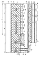
本実施形態のイメージセンサにおいて、黒基準領域29内の黒基準セル4(フォトダイオード40)の上方に、凹凸部を有する遮光膜61が設けられている。遮光膜61の凹凸部(突起部)62は、光の照射側に形成される。遮光膜61の凹凸部(突起部)62は、遮光膜61に照射される光を反射及び散乱させる。   In the image sensor of the present embodiment, a light shielding film 61 having an uneven portion is provided above the black reference cell 4 (photodiode 40) in the black reference region 29. The uneven part (projection part) 62 of the light shielding film 61 is formed on the light irradiation side. The concavo-convex part (projection part) 62 of the light shielding film 61 reflects and scatters the light irradiated to the light shielding film 61.

その遮光膜61は、例えば、マイクロレンズ60と同じ材料(透明膜)を用いて、層間絶縁膜71上方に、形成される。遮光膜61の表面の凹凸部62は、マイクロレンズ60を形成するための透明膜の表面を、例えば、エッチングを用いて、粗雑化することによって、形成される。この凹凸部62によって、遮光膜61の表面平坦度は、マイクロレンズ60の表面平坦度より低くなる。尚、図4において、遮光膜61の凹凸部62は、図示の簡単化のため均一性(周期性)を有するように図示されているが、これに限定されない。例えば、凹凸部62の形状は、ほとんど均一性を有さずに、ランダム(不均一)な形状を有している。   The light shielding film 61 is formed above the interlayer insulating film 71 using the same material (transparent film) as the microlens 60, for example. The uneven portion 62 on the surface of the light shielding film 61 is formed by roughening the surface of the transparent film for forming the microlens 60 using, for example, etching. Due to the uneven portion 62, the surface flatness of the light shielding film 61 becomes lower than the surface flatness of the microlens 60. In FIG. 4, the concavo-convex portion 62 of the light shielding film 61 is illustrated as having uniformity (periodicity) for simplification of illustration, but is not limited thereto. For example, the shape of the concavo-convex portion 62 has a random (non-uniform) shape with almost no uniformity.

凹凸部62を含む遮光膜61の最大膜厚は、基板表面に対して垂直方向におけるマイクロレンズ60の最大寸法(最大膜厚)よりも小さい。   The maximum film thickness of the light shielding film 61 including the uneven portion 62 is smaller than the maximum dimension (maximum film thickness) of the microlens 60 in the direction perpendicular to the substrate surface.

本実施形態において、遮光膜61は透明な材料を用いて形成されるため、光を透過させにくくするために、遮光膜61の表面粗さ(凹凸の段差)は、光を乱反射及び散乱させる大きさ及び密度に設定されている。例えば、遮光膜61における表面粗さは、例えば、マイクロレンズの厚さの10分の1程度の大きさを有している。例えば、マイクロレンズの膜厚が、4〜7μmである場合、遮光膜61は、ナノメートルオーダー(数百nm〜数十nm)の表面粗さを有する。   In the present embodiment, since the light shielding film 61 is formed using a transparent material, the surface roughness (uneven steps) of the light shielding film 61 is large enough to diffuse and scatter light in order to make it difficult to transmit light. The thickness and density are set. For example, the surface roughness of the light shielding film 61 is, for example, about 1/10 of the thickness of the microlens. For example, when the thickness of the microlens is 4 to 7 μm, the light shielding film 61 has a surface roughness on the order of nanometers (several hundred nm to several tens of nm).

黒基準領域29に対する光は、遮光膜61の表面の凹凸部62によって、反射又は散乱されるため、黒基準領域29において、遮光膜61の下方の層間絶縁膜71内に侵入する光は、低減する。   The light with respect to the black reference region 29 is reflected or scattered by the uneven portion 62 on the surface of the light shielding film 61, so that the light entering the interlayer insulating film 71 below the light shielding film 61 in the black reference region 29 is reduced. To do.

金属膜は、その性質上、ピンホール(微細な孔)を含んでいる。
さらに、イメージセンサチップ及びイメージセンサチップを含んでいるカメラモジュールは、装置のサイズの縮小が要求されているため、チップ及びモジュールは薄型化される傾向がある。そのため、イメージセンサチップを形成するための部材が薄くされ、それに伴って、遮光膜としての金属膜73の膜厚は、薄くなる。その結果として、遮光膜としての金属膜72,73に、ピンホールが、発生しやすくなっている。
The metal film includes pinholes (fine holes) due to its properties.
Furthermore, since the image sensor chip and the camera module including the image sensor chip are required to reduce the size of the device, the chip and the module tend to be thinned. Therefore, a member for forming the image sensor chip is thinned, and accordingly, the film thickness of the metal film 73 as the light shielding film is thinned. As a result, pinholes are easily generated in the metal films 72 and 73 as the light shielding films.

本実施形態のイメージセンサのように、光の照射される側の面が凸凹な(粗雑な)遮光膜61が層間絶縁膜71上に設けられていることによって、その凹凸部62による光の反射及び散乱が生じる。その結果として、凹凸部62を有する遮光膜61よりも下方に入射される光を低減でき、黒基準領域29に対する遮光性を向上できる。   As in the image sensor of this embodiment, the light-irradiated surface is provided with an uneven (coarse) light-shielding film 61 on the interlayer insulating film 71, so that the light is reflected by the uneven part 62. And scattering occurs. As a result, the light incident below the light shielding film 61 having the concavo-convex portion 62 can be reduced, and the light shielding property to the black reference region 29 can be improved.

それゆえ、黒基準領域29内の遮光膜としての金属膜73が、ピンホールのような光が通過する可能性がある欠陥を含んでいたとしても、光が黒基準領域29内のフォトダイオード(ダミーダイオード)40に入射されてしまうのを低減できる。これによって、黒基準領域29内の黒基準セル40から出力される基準電位が、遮光膜73を貫通した光をダミーダイオードが光電変換することによって変動するのを、抑制できる。   Therefore, even if the metal film 73 as the light shielding film in the black reference region 29 includes a defect such as a pinhole that allows light to pass through, the photodiode ( It is possible to reduce the incidence on the dummy diode 40. As a result, the reference potential output from the black reference cell 40 in the black reference region 29 can be prevented from changing due to the photoelectric conversion of the light that has penetrated the light shielding film 73 by the dummy diode.

したがって、本実施形態のイメージセンサは、画素データDsigによって形成される画像の色調が、より高精度で、入射光に対応する画像(被写体)の色調に再現できる。   Therefore, the image sensor of this embodiment can reproduce the color tone of the image formed by the pixel data Dsig with higher accuracy to the color tone of the image (subject) corresponding to the incident light.

また、凹凸を有する遮光膜61の厚さは、マイクロレンズ60の厚さより薄く、且つ、遮光膜としての金属膜72,73を厚くせずとも、黒基準領域29の遮光性を向上できるので、薄型なイメージセンサチップを提供できる。   In addition, since the thickness of the light-shielding film 61 having irregularities is smaller than the thickness of the microlens 60 and the metal films 72 and 73 as the light-shielding films are not thickened, the light-shielding property of the black reference region 29 can be improved. A thin image sensor chip can be provided.

黒基準領域29の遮光性を向上させるために、黒のフィルタや各色に対応する複数のフィルタが積層された膜が、黒基準領域29内に設けられる場合がある。後述するように、これらの場合、イメージセンサの製造工程の増加や、製造工程の加工難度の上昇が生じる。これに対して、本実施形態のイメージセンサにおいて、凹凸部62を有する遮光膜61は、基板表面に対して垂直方向においてマイクロレンズ60と同じ高さにおいて、マイクロレンズ60と同じ材料を用いて形成される。また、遮光膜61の凹凸部62は、パッド70の開口工程と実質的に同時に形成される。そのため、本実施形態のイメージセンサは、後述の製造方法によって、製造工程の増加や加工難度の上昇無しに、その表面が凸凹な遮光膜61を形成できる。それゆえ、製造コストや製造期間の増加無しに、色の再現性が向上したイメージセンサを形成できる。   In order to improve the light shielding property of the black reference region 29, a film in which a black filter or a plurality of filters corresponding to each color is stacked may be provided in the black reference region 29 in some cases. As will be described later, in these cases, an increase in the manufacturing process of the image sensor and an increase in processing difficulty of the manufacturing process occur. On the other hand, in the image sensor of this embodiment, the light shielding film 61 having the concavo-convex portion 62 is formed using the same material as the microlens 60 at the same height as the microlens 60 in the direction perpendicular to the substrate surface. Is done. The uneven portion 62 of the light shielding film 61 is formed substantially simultaneously with the opening process of the pad 70. Therefore, the image sensor of the present embodiment can form the light-shielding film 61 having an uneven surface by an after-mentioned manufacturing method without an increase in manufacturing steps or an increase in processing difficulty. Therefore, an image sensor with improved color reproducibility can be formed without an increase in manufacturing cost and manufacturing period.

以上のように、本実施形態の固体撮像装置によれば、形成される画像の画質を向上できる。   As described above, according to the solid-state imaging device of the present embodiment, the image quality of the formed image can be improved.

(b) 製造方法
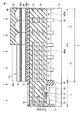
図3乃至図7を用いて、第1の実施形態の固体撮像装置(イメージセンサ)の製造方法について、説明する。図4乃至図7は、本実施形態のイメージセンサの製造方法の各工程における断面構造を示している。尚、本実施形態のイメージセンサの製造方法において、後述のイメージセンサの各構成要素の形成順序は、プロセスの整合性が確保されていれば、適宜変更されてもよい。
(B) Manufacturing method
A method for manufacturing the solid-state imaging device (image sensor) according to the first embodiment will be described with reference to FIGS. 4 to 7 show cross-sectional structures in the respective steps of the image sensor manufacturing method of the present embodiment. Note that in the image sensor manufacturing method of the present embodiment, the order in which components of the image sensor described later are formed may be appropriately changed as long as process consistency is ensured.

図4に示されるように、半導体基板10、例えば、P型シリコン基板10内に、P型及びN型のウェル領域15や素子分離層90,91が、それぞれ形成される。尚、半導体基板10は、SOI基板でもよい。   As shown in FIG. 4, P-type and N-type well regions 15 and element isolation layers 90 and 91 are formed in a semiconductor substrate 10, for example, a P-type silicon substrate 10. The semiconductor substrate 10 may be an SOI substrate.

ウェル領域15及び素子分離不純物層は、フォトリソグラフィ技術によって形成されたマスクや、イオン注入における不純物イオンの加速エネルギーの制御によって、半導体基板10内の所定の位置に、形成される。   The well region 15 and the element isolation impurity layer are formed at predetermined positions in the semiconductor substrate 10 by control of acceleration energy of impurity ions in ion implantation or a mask formed by a photolithography technique.

素子分離溝が、フォトリソグラフィ技術及びRIE(Reactive Ion Etching)法によって、半導体基板10内に形成される。素子分離溝内に、絶縁体が、CVD(Chemical Vapor Deposition)法又は塗布法によって埋め込まれ、素子分離絶縁膜95が半導体基板10内の所定の位置に形成される。   An element isolation trench is formed in the semiconductor substrate 10 by a photolithography technique and an RIE (Reactive Ion Etching) method. An insulator is embedded in the element isolation trench by a CVD (Chemical Vapor Deposition) method or a coating method, and an element isolation insulating film 95 is formed at a predetermined position in the semiconductor substrate 10.

これによって、半導体基板10内に、隣接する素子を電気的に分離する素子分離領域(絶縁膜又は不純物層)が形成され、画素アレイ20とこれに隣接する周辺領域7とが、それぞれ半導体基板10内に区画される。また、画素アレイ2内において、単位セル形成領域が、形成された素子分離領域によって定義される。単位セル形成領域は、少なくとも1つの画素形成領域(フォトダイオード形成領域)を含み、画素形成領域も素子分離領域によって定義されている。   Thereby, an element isolation region (insulating film or impurity layer) for electrically isolating adjacent elements is formed in the semiconductor substrate 10, and the pixel array 20 and the peripheral region 7 adjacent thereto are respectively connected to the semiconductor substrate 10. It is partitioned in. In the pixel array 2, a unit cell formation region is defined by the formed element isolation region. The unit cell formation region includes at least one pixel formation region (photodiode formation region), and the pixel formation region is also defined by the element isolation region.

フォトリソグラフィ技術によって、レジストマスク(図示せず)が半導体基板10上に、形成される。レジストマスクは、フォトダイオード形成領域に対応して、開口部が形成されている。そのレジストマスクを用いて、不純物層30,40が、イオン注入法によって半導体基板10内に、形成される。半導体基板10が、P型の半導体基板である場合、不純物層30,40は、例えば、少なくとも1つのN型の不純物層から形成される。フォトダイオードは、複数の不純物層によって形成されてもよい。これによって、イメージセンサの各画素に対応するフォトダイオード3,4が、画素アレイ2内に、形成される。尚、フォトダイオード3,4の特性を向上させるため、複数のP型及びN型の不純物層が、フォトダイオード形成領域内に、形成されてもよい。   A resist mask (not shown) is formed on the semiconductor substrate 10 by photolithography. The resist mask has an opening corresponding to the photodiode formation region. Using the resist mask, impurity layers 30 and 40 are formed in the semiconductor substrate 10 by ion implantation. When the semiconductor substrate 10 is a P-type semiconductor substrate, the impurity layers 30 and 40 are formed of, for example, at least one N-type impurity layer. The photodiode may be formed by a plurality of impurity layers. As a result, photodiodes 3 and 4 corresponding to the respective pixels of the image sensor are formed in the pixel array 2. In order to improve the characteristics of the photodiodes 3 and 4, a plurality of P-type and N-type impurity layers may be formed in the photodiode formation region.

フローティングディフュージョンとしての不純物層(図示せず)が、フォトリソグラフィ技術及びイオン注入法によって、画素アレイ2のセル形成領域20内の所定の位置において、半導体基板10内に形成される。   An impurity layer (not shown) as a floating diffusion is formed in the semiconductor substrate 10 at a predetermined position in the cell formation region 20 of the pixel array 2 by photolithography and ion implantation.

半導体基板10上に、ゲート絶縁膜52が、例えば、熱酸化法によって、半導体基板10上に形成される。ゲート絶縁膜52上に、シリコン層が、CVD法により、堆積される。そして、フォトリソグラフィ技術及びRIE法によって、所定のゲート長及びゲート幅のゲート電極51が、ゲート絶縁膜52を挟んで、半導体基板10の表面(第1の面)上に形成される。例えば、形成されたゲート電極51がマスクとして用いられ、イオン注入法によって、ソース及びドレインとしての不純物層53が、半導体基板10内に形成される。これによって、半導体基板10の表面上に、単位セルを形成するための電界効果トランジスタ及び周辺回路を形成するための電界効果トランジスタTrが、画素アレイ2内及び周辺領域7内にそれぞれ形成される。   A gate insulating film 52 is formed on the semiconductor substrate 10 by, for example, a thermal oxidation method on the semiconductor substrate 10. A silicon layer is deposited on the gate insulating film 52 by a CVD method. Then, a gate electrode 51 having a predetermined gate length and gate width is formed on the surface (first surface) of the semiconductor substrate 10 with the gate insulating film 52 interposed therebetween by a photolithography technique and an RIE method. For example, the formed gate electrode 51 is used as a mask, and an impurity layer 53 as a source and a drain is formed in the semiconductor substrate 10 by ion implantation. Thereby, a field effect transistor for forming a unit cell and a field effect transistor Tr for forming a peripheral circuit are formed in the pixel array 2 and the peripheral region 7 on the surface of the semiconductor substrate 10, respectively.

尚、単位セルの電界効果トランジスタ及び周辺回路の電界効果トランジスタTrは、同時の工程で形成されてもよいし、それぞれ別の工程で形成されてもよい。   The field effect transistor of the unit cell and the field effect transistor Tr of the peripheral circuit may be formed in the same process, or may be formed in different processes.

素子が形成された半導体基板10の表面(第1の面)上に、多層配線技術により、層間絶縁膜71、金属膜72,73,75及びプラグCP,76が、配線レベル毎に順次形成される。   On the surface (first surface) of the semiconductor substrate 10 on which the element is formed, an interlayer insulating film 71, metal films 72, 73, 75 and plugs CP, 76 are sequentially formed for each wiring level by a multilayer wiring technique. The

例えば、最下層の層間絶縁膜は、トランジスタTrのゲート電極51及びフォトダイオード30,40の上面を覆うように、CVD(Chemical Vapor Deposition)法によって、堆積される。そして、堆積された層間絶縁膜の上面が、例えば、CMP(Chemical Mechanical Polishing)法を用いて平坦化される。ゲート電極の上部や不純物層(ソース/ドレイン又はコンタクト領域)の上部を露出させるように、コンタクトホールが、層間絶縁膜71内に、フォトリソグラフィ技術及びRIE法を用いて、形成される。コンタクトプラグCPは、形成されたコンタクトホール内に埋め込まれる。   For example, the lowermost interlayer insulating film is deposited by a CVD (Chemical Vapor Deposition) method so as to cover the gate electrode 51 of the transistor Tr and the upper surfaces of the photodiodes 30 and 40. Then, the upper surface of the deposited interlayer insulating film is planarized using, for example, a CMP (Chemical Mechanical Polishing) method. A contact hole is formed in the interlayer insulating film 71 using the photolithography technique and the RIE method so as to expose the upper part of the gate electrode and the upper part of the impurity layer (source / drain or contact region). The contact plug CP is embedded in the formed contact hole.

アルミニウムや銅などの金属膜が、例えば、スパッタ法によって、最下層の層間絶縁膜上及びコンタクトプラグCP上に堆積される。堆積された金属膜は、フォトリソグラフィ技術及びRIE法によって、コンタクトプラグCP1に接続されるように、所定の形状に加工される。これと実質的に同様の工程によって、各配線レベルにおいて、層間絶縁膜、ビアプラグ79及び複数の金属膜72,73,75が、多層配線技術によって、下層(基板表面側)の配線レベルから順次形成される。   A metal film such as aluminum or copper is deposited on the lowermost interlayer insulating film and the contact plug CP, for example, by sputtering. The deposited metal film is processed into a predetermined shape so as to be connected to the contact plug CP1 by a photolithography technique and an RIE method. By substantially the same process, an interlayer insulating film, a via plug 79, and a plurality of metal films 72, 73, and 75 are sequentially formed from the wiring level on the lower layer (substrate surface side) by multilayer wiring technology at each wiring level. Is done.

これによって、画素アレイ2内において、遮光膜72,73としての金属膜72,73が形成され、周辺領域7内において、配線75としての金属膜75が形成される。例えば、遮光膜(金属膜)72,73は、100nmから400nm程度の膜厚になるように、形成される。   As a result, the metal films 72 and 73 as the light shielding films 72 and 73 are formed in the pixel array 2, and the metal film 75 as the wiring 75 is formed in the peripheral region 7. For example, the light shielding films (metal films) 72 and 73 are formed to have a film thickness of about 100 nm to 400 nm.

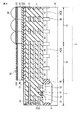
図5に示されるように、例えば、再配線形成技術によって、再配線層70が、配線75に接続されるように、層間絶縁膜72上に、形成される。再配線層70は、例えば、パッドとして用いられる。層間絶縁膜71上に、絶縁層(例えば、樹脂層)77が形成される。この後、オーバーコート層68Aが、再配線層70及び絶縁層77上に形成される。ここで、オーバーコート層68Aは、平坦化層、保護層及び接着層を含む積層膜である。   As shown in FIG. 5, the rewiring layer 70 is formed on the interlayer insulating film 72 so as to be connected to the wiring 75 by, for example, a rewiring formation technique. The rewiring layer 70 is used as a pad, for example. An insulating layer (for example, a resin layer) 77 is formed on the interlayer insulating film 71. Thereafter, an overcoat layer 68 </ b> A is formed on the rewiring layer 70 and the insulating layer 77. Here, the overcoat layer 68A is a laminated film including a planarization layer, a protective layer, and an adhesive layer.

そして、カラーフィルタ65が、画素アレイ2の撮像領域21内において、各画素30に対応するように、オーバーコート層68A上に形成される。例えば、単色のカラーフィルタ(ダミーフィルタ)66が、画素アレイ2の黒基準領域29内において、オーバーコート層68A上に形成される。パッドとしての再配線層70上方において、カラーフィルタは、形成されない。   Then, the color filter 65 is formed on the overcoat layer 68 </ b> A so as to correspond to each pixel 30 in the imaging region 21 of the pixel array 2. For example, a single color filter (dummy filter) 66 is formed on the overcoat layer 68 </ b> A in the black reference region 29 of the pixel array 2. A color filter is not formed above the rewiring layer 70 as a pad.

カラーフィルタ65,66上及びオーバーコート層68A上に、オーバーコート層69Aが、形成される。そして、マイクロレンズを形成するための透明膜(以下、レンズ形成層とよぶ)が、オーバーコート層69A上に、形成される。レンズ形成層60,61Aは、高い透過性を有する材料が用いられ、例えば、有機膜又は樹脂が用いられる。ただし、レンズ形成層は、ガラスなどの無機化合物層でもよい。尚、オーバーコート層68A,69Aも透過性を有するのは、もちろんである。   Overcoat layer 69A is formed on color filters 65 and 66 and overcoat layer 68A. Then, a transparent film (hereinafter referred to as a lens forming layer) for forming the microlens is formed on the overcoat layer 69A. The lens forming layers 60 and 61A are made of a highly permeable material, for example, an organic film or a resin. However, the lens forming layer may be an inorganic compound layer such as glass. Of course, the overcoat layers 68A and 69A also have transparency.

例えば、レンズ形成層の膜厚は、パッド70上のオーバーコート層68A,69Aの膜厚よりも厚い。例えば、レンズ形成層61Aは、その形成時において、1μmから10μm程度の膜厚を有する。   For example, the thickness of the lens forming layer is larger than the thickness of the overcoat layers 68A and 69A on the pad 70. For example, the lens forming layer 61A has a film thickness of about 1 μm to 10 μm when formed.

画素アレイ2の撮像領域21上方において、そのレンズ形成層が、例えば、エッチング(RIE法)によって、半球状(レンズ状)に加工され、マイクロレンズ60が、各フォトダイオード30に対応するように、形成される。黒基準領域29内のレンズ形成層は、レジストマスクで覆われ、エッチングされない。尚、マイクロレンズを形成するための加工は、レンズ形成層の熱変化を利用した加工処理や成型処理(モールド処理)などによって、実行されてもよい。   Above the imaging region 21 of the pixel array 2, the lens formation layer is processed into a hemisphere (lens shape) by, for example, etching (RIE method), and the microlens 60 corresponds to each photodiode 30. It is formed. The lens forming layer in the black reference region 29 is covered with a resist mask and is not etched. In addition, the process for forming the microlens may be performed by a process using a thermal change of the lens forming layer, a molding process (molding process), or the like.

周辺領域7内のレンズ形成層は、例えば、マイクロレンズ60の形成とは別途の工程において、フォトリソグラフィ技術及びエッチングによって、選択的に除去される。   The lens forming layer in the peripheral region 7 is selectively removed by, for example, a photolithography technique and etching in a process separate from the formation of the microlens 60.

図6に示されるように、マイクロレンズ60が形成された後、パッド70の開口のためのパターニングが、実行される。そのため、フォトリソグラフィ技術によって、マイクロレンズ60を覆うように、レジストマスク96が形成される。レジストマスク96は、パッド70の上方から選択的に除去され、パッド70を覆っているオーバーコート層69Aが露出される。   As shown in FIG. 6, after the micro lens 60 is formed, patterning for opening the pad 70 is performed. Therefore, a resist mask 96 is formed so as to cover the microlens 60 by photolithography. The resist mask 96 is selectively removed from above the pad 70, and the overcoat layer 69A covering the pad 70 is exposed.

この際、黒基準領域29内において、レジストマスクは除去される。又は、黒基準領域29内のレンズ形成層61A上のレジストマスク96X(図6中において、破線で示す)の膜厚が、ハーフトーンマスク(レチクル)による中間露光によって、マイクロレンズ60を覆うレジストマスク96の膜厚より薄くされる。この場合、黒基準領域69内のレジストマスク96Xは、例えば、マイクロレンズ60を覆うレジストマスク96と、同時に形成される。   At this time, the resist mask is removed in the black reference region 29. Alternatively, the resist mask 96X (shown by a broken line in FIG. 6) on the lens formation layer 61A in the black reference region 29 has a film thickness that covers the microlens 60 by intermediate exposure using a halftone mask (reticle). The film thickness is made thinner than 96. In this case, the resist mask 96X in the black reference region 69 is formed simultaneously with the resist mask 96 that covers the microlens 60, for example.

マイクロレンズ60を覆うレジストマスク96が形成された後、図7に示されるように、エッチング(例えば、RIE法)が実行される。これによって、パッド70上のオーバーコート層が除去され、パッド70の上面が露出する。例えば、パッド70の上面のオーバーコート層を除去するためのエッチングは、酸素(O)系ガスとフッ素(F)系ガスとの混合ガスを用いて、1Torr(1.33×10Pa)の真空度で、300秒から600秒の期間、実行される。尚、オーバーコート層の材料に応じて、フッ素系ガスが、酸素ガスに添加されない場合もある。また、エッチングのための電力(例えば、RFパワー)は、ガス圧やエッチング時間に応じて、適宜調整される。 After the resist mask 96 covering the microlens 60 is formed, etching (for example, RIE method) is performed as shown in FIG. As a result, the overcoat layer on the pad 70 is removed, and the upper surface of the pad 70 is exposed. For example, the etching for removing the overcoat layer on the upper surface of the pad 70 is performed using a mixed gas of oxygen (O) gas and fluorine (F) gas at 1 Torr (1.33 × 10 2 Pa). Performed at a vacuum level for a period of 300 to 600 seconds. Depending on the material of the overcoat layer, the fluorine-based gas may not be added to the oxygen gas. Further, the power for etching (for example, RF power) is appropriately adjusted according to gas pressure and etching time.

このパッド70の開口のためのエッチングの際、画素アレイ2に対しても、エッチングが施される。撮像領域21内のマイクロレンズ60は、レジストマスク96に覆われているので、エッチングされない。
これに対して、黒基準領域29内において、レンズ形成層61は露出している。そのため、レンズ形成層61の表面はエッチングされる。また、レンズ形成層61がマイクロレンズ60を覆うマスク96より薄いレジストマスク96Xによって覆われている場合、レンズ形成層61がオーバーエッチングされる。つまり、黒基準領域29内において、レンズ形成層61を覆うレジストマスク96Xが除去された後、レンズ形成層61の表面がエッチングされる。
During the etching for opening the pad 70, the pixel array 2 is also etched. Since the microlens 60 in the imaging region 21 is covered with the resist mask 96, it is not etched.
On the other hand, the lens forming layer 61 is exposed in the black reference region 29. Therefore, the surface of the lens forming layer 61 is etched. When the lens forming layer 61 is covered with a resist mask 96X that is thinner than the mask 96 that covers the microlens 60, the lens forming layer 61 is over-etched. That is, in the black reference region 29, after the resist mask 96X covering the lens forming layer 61 is removed, the surface of the lens forming layer 61 is etched.

エッチングによって、黒基準領域29内のレンズ形成層(例えば、有機膜)の表面が荒れ、凸凹な表面を有する遮光膜(レンズ形成層)61が形成される。例えば、マイクロレンズの膜厚が、4〜7μmである場合、遮光膜61は、ナノメートルオーダー(数百nm〜数十nm)の表面粗さを有する。エッチング荒れに起因する遮光膜61の表面の凹凸部62によって、黒基準領域29に対する光は、乱反射又は散乱され、遮光膜61の下方に侵入する光は、低減する。   By etching, the surface of the lens forming layer (for example, organic film) in the black reference region 29 is roughened, and a light shielding film (lens forming layer) 61 having an uneven surface is formed. For example, when the thickness of the microlens is 4 to 7 μm, the light shielding film 61 has a surface roughness on the order of nanometers (several hundred nm to several tens of nm). The light with respect to the black reference region 29 is irregularly reflected or scattered by the concavo-convex portion 62 on the surface of the light shielding film 61 due to etching roughness, and the light that enters the light shielding film 61 is reduced.

このように、遮光膜61の表面に形成された凸凹部62は、パッド70の開口と同時に形成されるため、遮光膜61が形成されても、製造工程が増加することはない。尚、レンズ形成層61の表面を粗くするための処理のみならば、エッチングの期間は、10秒から30秒程度でもよい。パッドの開口を行うためのエッチング条件は、オーバーコート層の材料や粗面化されるレンズ形成層の材料に応じて、適宜変更されるのは、もちろんである。   Thus, since the convex / concave portion 62 formed on the surface of the light shielding film 61 is formed simultaneously with the opening of the pad 70, even if the light shielding film 61 is formed, the manufacturing process does not increase. If only the process for roughening the surface of the lens forming layer 61 is performed, the etching period may be about 10 to 30 seconds. Of course, the etching conditions for opening the pad are appropriately changed according to the material of the overcoat layer and the material of the lens forming layer to be roughened.

パッド70の開口及び遮光膜61の表面の粗雑化の後、マイクロレンズ60上のレジストマスク60が除去される。   After the opening of the pad 70 and the surface of the light shielding film 61 are roughened, the resist mask 60 on the microlens 60 is removed.

以上の製造工程によって、図4に示される本実施形態のイメージセンサが作製される。   Through the above manufacturing process, the image sensor of the present embodiment shown in FIG. 4 is manufactured.

遮光膜としての金属膜はピンホールを含む可能性があり、かつ、イメージセンサの薄型化に伴って、金属膜の膜厚が薄くされる傾向がある。
本実施形態のイメージセンサのように、光が照射される側の面が凸凹な遮光膜61が黒基準領域29内に形成されることによって、黒基準領域29に照射される光は、遮光膜61の表面の凹凸部62によって、反射又は散乱され、遮光膜61の下方の層間絶縁膜71内に侵入する光は、低減する。すなわち、凹凸部62を有する遮光膜61によって、黒基準領域29に対する遮光性を向上できる。
それゆえ、黒基準領域29内の遮光膜(金属膜)73がピンホールのような光が通過する可能性がある欠陥を含んでいたとしても、黒基準領域29内に漏れ込んだ光が、黒基準領域29内のフォトダイオード(ダミーダイオード)40に入射されるのを低減できる。これによって、黒基準領域29内の黒基準セル40から出力される基準電位が、遮光膜73を貫通した光が光電変換されることによって変動するのを、抑制できる。
The metal film as the light shielding film may contain pinholes, and the thickness of the metal film tends to be reduced as the image sensor becomes thinner.
As in the image sensor of the present embodiment, the light shielding film 61 having an uneven surface on which light is irradiated is formed in the black reference area 29, so that the light irradiated to the black reference area 29 Light that is reflected or scattered by the concavo-convex portion 62 on the surface of 61 and enters the interlayer insulating film 71 below the light shielding film 61 is reduced. That is, the light shielding property with respect to the black reference region 29 can be improved by the light shielding film 61 having the uneven portion 62.
Therefore, even if the light shielding film (metal film) 73 in the black reference region 29 includes a defect such as a pinhole, light leaked into the black reference region 29 The incidence on the photodiode (dummy diode) 40 in the black reference region 29 can be reduced. Thereby, it is possible to suppress the reference potential output from the black reference cell 40 in the black reference region 29 from fluctuating due to photoelectric conversion of the light that has penetrated the light shielding film 73.

したがって、本実施形態のイメージセンサの製造方法は、入射光に対応する画像(被写体)の色調をより高精度に再現できるイメージセンサを、形成できる。   Therefore, the image sensor manufacturing method of the present embodiment can form an image sensor that can reproduce the color tone of an image (subject) corresponding to incident light with higher accuracy.

これにともなって、本実施形態は、金属の遮光膜73及びそれを覆う層間絶縁膜71の膜厚及び積層数が、遮光性を向上させるために増加するのを、抑制できる。それゆえ、本実施形態のイメージセンサの製造方法は、薄型化したイメージセンサを提供できる。   Accordingly, the present embodiment can suppress an increase in the thickness and the number of stacked layers of the metal light shielding film 73 and the interlayer insulating film 71 covering the metal light shielding film 73 in order to improve the light shielding property. Therefore, the image sensor manufacturing method of the present embodiment can provide a thin image sensor.

黒基準領域29の遮光性を向上させるために、黒のフィルタや各色に対応する複数のフィルタが積層された膜が、黒基準領域29内に設けられる場合がある。黒のフィルタが黒基準領域29内に形成される場合、イメージセンサの製造工程が増加する。カラーフィルタが含む各色のフィルタの積層膜(例えば、赤、青及び緑の3層膜)が、黒基準領域29内に形成される場合、黒基準領域29と他の領域7,21との間に、積層されたフィルタに起因する大きな段差が生じ、マイクロレンズの形成やパッドの開口が、困難になる。
これに対して、本実施形態のイメージセンサの製造方法は、凸凹な表面を有する遮光膜61を、例えば、マイクロレンズの形成部材のようなイメージセンサが含む通常の部材を用いて、マイクロレンズ及びパッドの開口と実質的に同時の工程で、形成できる。それゆえ、製造コストや製造期間の増加無しに、色の再現性が向上したイメージセンサを形成できる。
In order to improve the light shielding property of the black reference region 29, a film in which a black filter or a plurality of filters corresponding to each color is stacked may be provided in the black reference region 29 in some cases. When the black filter is formed in the black reference region 29, the manufacturing process of the image sensor is increased. When a laminated film (for example, a three-layer film of red, blue, and green) of each color filter included in the color filter is formed in the black reference region 29, it is between the black reference region 29 and the other regions 7, 21. In addition, a large step due to the stacked filters is generated, and it becomes difficult to form a microlens and to open a pad.
On the other hand, in the image sensor manufacturing method of the present embodiment, the microlens and the light shielding film 61 having an uneven surface are used, for example, by using a normal member included in the image sensor such as a microlens forming member. It can be formed by substantially the same process as the opening of the pad. Therefore, an image sensor with improved color reproducibility can be formed without an increase in manufacturing cost and manufacturing period.

以上のように、本実施形態の固体撮像装置の製造方法によれば、形成される画像の画質を向上できる。   As described above, according to the method for manufacturing the solid-state imaging device of the present embodiment, the image quality of the formed image can be improved.

(2) 第2の実施形態
図8を参照して、第2の実施形態の固体撮像装置及びその製造方法について説明する。尚、第2の実施形態において、第1の実施形態と共通する部材及び製造工程に関する説明は、必要に応じて行う。
(2) Second embodiment
With reference to FIG. 8, a solid-state imaging device and a manufacturing method thereof according to the second embodiment will be described. Note that in the second embodiment, explanations regarding members and manufacturing steps common to the first embodiment will be made as necessary.

第1の実施形態において、マイクロレンズ60を形成するためのレンズ形成層を用いて、凸凹な表面を有する遮光膜61が形成される。
ただし、黒基準領域29内のフォトダイオード40及び金属の遮光膜73の上方に、表面が粗雑化された遮光膜が設けられていれば、遮光膜の材料及び基板表面に対して垂直方向における遮光膜の形成位置(基板表面からの高さ)は、限定されない。
In the first embodiment, the light shielding film 61 having an uneven surface is formed using a lens forming layer for forming the microlens 60.
However, if a light-shielding film having a roughened surface is provided above the photodiode 40 and the metal light-shielding film 73 in the black reference region 29, light shielding in a direction perpendicular to the material of the light-shielding film and the substrate surface is performed. The film formation position (height from the substrate surface) is not limited.

例えば、図8に示されるように、カラーフィルタ65,66上のオーバーコート層69,69Xを用いて、凹凸部62を有する遮光膜69Xが形成されてもよい。この場合、遮光膜69Xは、オーバーコート層69と同じ材料からなり、透明性を有する材料(透明膜)を用いて形成される。遮光膜69Xは、基板表面に対して垂直方向において、オーバーコート層69と同じ高さに設けられている。   For example, as illustrated in FIG. 8, the light shielding film 69 </ b> X having the uneven portion 62 may be formed using the overcoat layers 69 and 69 </ b> X on the color filters 65 and 66. In this case, the light shielding film 69X is made of the same material as the overcoat layer 69 and is formed using a transparent material (transparent film). The light shielding film 69X is provided at the same height as the overcoat layer 69 in the direction perpendicular to the substrate surface.

尚、凸凹な表面を有する遮光膜は、カラーフィルタ66又はその下方のオーバーコート層68を用いて形成されてもよい。   The light shielding film having an uneven surface may be formed using the color filter 66 or the overcoat layer 68 below the color filter 66.

凸凹な表面を有する遮光膜69Xがオーバーコート層を用いて形成される場合、図5及び図6に示される工程において、例えば、黒基準領域29内のレンズ形成層61Aが除去される。   When the light shielding film 69X having an uneven surface is formed using an overcoat layer, for example, the lens forming layer 61A in the black reference region 29 is removed in the steps shown in FIGS.

そして、図7に示される工程と実質的に同じ工程によって、黒基準領域29内のオーバーコート層69Aの上面が露出される、或いは、オーバーコート層69A上に、マイクロレンズ60を覆うレジストマスクより薄いレジストマスクが形成される。ただし、プロセスの共通化のため、黒基準領域29内のレジストマスクの膜厚は、パッド70の開口のためのエッチング時に、黒基準領域19内のオーバーコート層69Aがオーバーエッチングされる膜厚であって、且つ、黒基準領域29内のオーバーコート層69Aがエッチングによって除去されない膜厚に設定されることが、好ましい。   Then, the upper surface of the overcoat layer 69A in the black reference region 29 is exposed by a process substantially the same as the process shown in FIG. 7, or from a resist mask that covers the microlens 60 on the overcoat layer 69A. A thin resist mask is formed. However, for the common process, the film thickness of the resist mask in the black reference region 29 is such that the overcoat layer 69A in the black reference region 19 is over-etched during the etching for opening the pad 70. In addition, it is preferable that the overcoat layer 69A in the black reference region 29 is set to a thickness that is not removed by etching.

尚、オーバーコート層69Xをオーバーエッチングすることが可能であれば、図5及び図6に示される工程において、レンズ形成層を黒基準領域29内に残存させてもよい。   If the overcoat layer 69X can be over-etched, the lens forming layer may be left in the black reference region 29 in the steps shown in FIGS.

このように、本実施形態のイメージセンサは、凹凸部62を有する遮光膜69Xが、オーバーコート層によって形成される。この場合でもあって、オーバーコート層からなる遮光膜69Xの凹凸部62による光の反射及び散乱によって、黒基準領域29内のダミーダイオード40に入射される光を低減できる。この結果として、ダミーダイオード40の光電変換に起因する基準電位の変動を抑制でき、形成される画像データの色調の再現性を向上できる。
また、本実施形態のイメージセンサの製造方法において、オーバーコート層を用いて凹凸部62を有する遮光膜69Xが形成された場合であっても、形成部材及び形成プロセスの共通化によって、製造工程を増加させずに、本実施形態のイメージセンサを形成できる。
As described above, in the image sensor of this embodiment, the light shielding film 69X having the uneven portion 62 is formed by the overcoat layer. Even in this case, the light incident on the dummy diode 40 in the black reference region 29 can be reduced by the reflection and scattering of the light by the concavo-convex portion 62 of the light shielding film 69X made of the overcoat layer. As a result, fluctuations in the reference potential due to the photoelectric conversion of the dummy diode 40 can be suppressed, and the color tone reproducibility of the formed image data can be improved.
Further, in the image sensor manufacturing method of the present embodiment, even when the light shielding film 69X having the concavo-convex portion 62 is formed using the overcoat layer, the manufacturing process is performed by sharing the forming member and the forming process. The image sensor of this embodiment can be formed without increasing the number.

以上のように、第2の実施形態の固体撮像装置及びその製造方法によれば、形成される画像の画質を向上できる固体撮像装置を提供できる。   As described above, according to the solid-state imaging device and the manufacturing method thereof according to the second embodiment, it is possible to provide a solid-state imaging device that can improve the image quality of the formed image.

(3) 変形例
図9及び図10を用いて、本実施形態の固体撮像装置の変形例について説明する。尚、第1及び第2の実施形態の構成要素と共通の部材に関して、重複する説明は、必要に応じて行う。
(3) Modification
A modification of the solid-state imaging device according to the present embodiment will be described with reference to FIGS. In addition, the overlapping description regarding the member common to the component of 1st and 2nd embodiment is performed as needed.

図9に示されるように、黒基準領域29内に、半球状の遮光膜60Xが設けられてもよい。遮光膜60Xは、マイクロレンズ60と同じ材料を用いて、マイクロレンズ60と共通の工程を用いて同時に形成される。遮光膜60Xは、レンズとして機能を有していてもよいし、上述のように、表面の粗雑化(エッチング荒れ)による凹凸部によって、レンズとしての機能が消失していていもよい。また、遮光膜60Xの上端が、平坦(直線)になっていてもよい。   As shown in FIG. 9, a hemispherical light shielding film 60 </ b> X may be provided in the black reference region 29. The light shielding film 60 </ b> X is formed at the same time using the same material as the microlens 60 and using the same process as the microlens 60. The light shielding film 60 </ b> X may have a function as a lens, or the function as a lens may be lost due to uneven portions due to roughening of the surface (etching roughness) as described above. Further, the upper end of the light shielding film 60X may be flat (straight).

例えば、遮光膜60Xがレンズとしての機能を有している場合、半球状の遮光膜60Xによって、基板表面に対して斜め方向からの光が、配線及び遮光膜の隙間を通過して、黒基準領域29内のダミーダイオード40に直接入射されてしまうのを、抑制できる。   For example, when the light shielding film 60X has a function as a lens, the hemispherical light shielding film 60X allows light from an oblique direction with respect to the substrate surface to pass through the gap between the wiring and the light shielding film, thereby obtaining a black reference. Direct incidence on the dummy diode 40 in the region 29 can be suppressed.

図10に示されるように、本実施形態のイメージセンサは、裏面照射型イメージセンサでもよい。
裏面照射型イメージセンサは、基板の裏面側が、被写体からの光の照射面となっている。裏面照射型イメージセンサは、素子(例えば、トランジスタのゲート電極)を覆う層間絶縁膜が設けられた面(表面)とは反対側の面(裏面)側に、カラーフィルタ65及びマイクロレンズ60が設けられている。本変形例のイメージセンサにおいて、裏面照射型イメージセンサの照射面側、すなわち、半導体基板10の裏面側に、凸凹な表面を有する遮光膜61が設けられる。
As shown in FIG. 10, the image sensor of the present embodiment may be a backside illuminated image sensor.
In the back side illumination type image sensor, the back side of the substrate is an irradiation surface of light from the subject. The back-illuminated image sensor is provided with a color filter 65 and a microlens 60 on the surface (back surface) opposite to the surface (front surface) provided with an interlayer insulating film covering an element (for example, a gate electrode of a transistor). It has been. In the image sensor of this modification, a light shielding film 61 having an uneven surface is provided on the irradiation surface side of the back-illuminated image sensor, that is, on the back surface side of the semiconductor substrate 10.

この場合、金属膜からなる遮光膜72A,73Aが、半導体基板10の裏面上の絶縁膜89を介して、基板10の裏面側に、設けられている。金属膜からなる遮光膜73Aは、黒基準領域29内において、黒基準セル4と半導体基板10の裏面上の絶縁膜89との間に設けられている。遮光膜73Aは、黒基準セル4及び電界効果トランジスタTrの下方(照射面側)を覆っている。遮光膜72A,73Aは、絶縁膜67に覆われている。   In this case, light shielding films 72 </ b> A and 73 </ b> A made of a metal film are provided on the back surface side of the substrate 10 via the insulating film 89 on the back surface of the semiconductor substrate 10. The light shielding film 73 A made of a metal film is provided between the black reference cell 4 and the insulating film 89 on the back surface of the semiconductor substrate 10 in the black reference region 29. The light shielding film 73A covers the lower side (irradiation surface side) of the black reference cell 4 and the field effect transistor Tr. The light shielding films 72A and 73A are covered with an insulating film 67.

裏面照射型イメージセンサにおいて、支持基板19が、接着層18によって、基板表面側の層間絶縁膜71に貼り付けられている。   In the back-illuminated image sensor, the support substrate 19 is attached to the interlayer insulating film 71 on the substrate surface side by the adhesive layer 18.

例えば、パッド80は、半導体基板10の裏面側に設けられている。半導体基板10の表面側から裏面側へ貫通する貫通ビア81を介して、層間絶縁膜71内の配線75に接続される。貫通ビア81は、TSV技術によって形成される。貫通ビア81と半導体基板10との間には、絶縁膜88が設けられ、パッド80と半導体基板10との間には、絶縁膜89が設けられている。   For example, the pad 80 is provided on the back side of the semiconductor substrate 10. The semiconductor substrate 10 is connected to a wiring 75 in the interlayer insulating film 71 through a through via 81 penetrating from the front surface side to the back surface side. The through via 81 is formed by TSV technology. An insulating film 88 is provided between the through via 81 and the semiconductor substrate 10, and an insulating film 89 is provided between the pad 80 and the semiconductor substrate 10.

金属の遮光膜72A,73Aは、例えば、半導体基板10の裏面上に設けられたパッド80と実質的に同時の工程で形成される。   The metal light shielding films 72A and 73A are formed, for example, in substantially the same process as the pad 80 provided on the back surface of the semiconductor substrate 10.

本変形例の裏面照射型イメージセンサは、例えば、以下のように形成される。
図4に示される工程と同様に、素子30,40,Tr、層間絶縁膜71及び配線(パッド)75,70が形成された半導体基板10内に対して、支持基板19が、接着層18を介して層間絶縁膜71に貼り付けられる。そして、ウェットエッチングやCMP法によって、半導体基板10の裏面側がエッチングされ、半導体基板10が薄くされる。
TSV技術によって、貫通ホール及び貫通ビア81が形成される。この後、絶縁膜89、パッド80及び遮光膜72A,73Aが順次形成される。
The backside illuminated image sensor of this modification is formed as follows, for example.
Similar to the process shown in FIG. 4, the support substrate 19 attaches the adhesive layer 18 to the semiconductor substrate 10 on which the elements 30, 40, Tr, the interlayer insulating film 71 and the wirings (pads) 75, 70 are formed. It is affixed to the interlayer insulation film 71 via the via. Then, the back side of the semiconductor substrate 10 is etched by wet etching or CMP, and the semiconductor substrate 10 is thinned.
Through holes and through vias 81 are formed by the TSV technique. Thereafter, the insulating film 89, the pad 80, and the light shielding films 72A and 73A are sequentially formed.

そして、パッド80及び遮光膜72A,73A上に、図5及び図6に示される工程と実質的に同じ工程によって、オーバーコート層68,69、カラーフィルタ65及びマイクロレンズ60が、半導体基板10の裏面側に、順次形成される。
図7に示される工程と実質的に同様に、パッド80上のオーバーコート層がエッチングによって除去するのと同時に、レンズ形成層61(又はオーバーコート層69)が、エッチング条件下にさらされる。エッチング荒れによって、表面が凸凹な遮光膜61が、半導体基板10の裏面側に形成される。
Then, the overcoat layers 68 and 69, the color filter 65, and the microlens 60 are formed on the pad 80 and the light shielding films 72 </ b> A and 73 </ b> A by substantially the same steps as those shown in FIGS. 5 and 6. It is formed sequentially on the back side.
Substantially similar to the process shown in FIG. 7, the lens-forming layer 61 (or overcoat layer 69) is exposed to etching conditions at the same time as the overcoat layer on the pad 80 is removed by etching. Due to the etching roughness, a light shielding film 61 having a rough surface is formed on the back side of the semiconductor substrate 10.

これによって、図10に示される変形例の裏面照射型イメージセンサが形成される。   As a result, the back-illuminated image sensor of the modification shown in FIG. 10 is formed.

図9及び図10に示される変形例のイメージセンサにおいても、黒基準領域29に入射される光を低減でき、黒基準領域29に対する遮光性を向上できる。   Also in the image sensor of the modification shown in FIG. 9 and FIG. 10, the light incident on the black reference region 29 can be reduced, and the light shielding property to the black reference region 29 can be improved.

したがって、本実施形態の変形例のイメージセンサは、第1及び第2の実施形態と同様に、形成される画像の画質を向上できる。   Therefore, the image sensor of the modification of this embodiment can improve the image quality of the image formed similarly to the 1st and 2nd embodiment.

尚、黒基準領域に対する遮光性をさらに向上させるために、凹凸部62を有する遮光膜に加えて、黒基準領域29内に設けられるダミーフィルタに、黒のフィルタや複数のフィルタの積層膜を用いてもよい。   In order to further improve the light shielding property with respect to the black reference region, a black filter or a laminated film of a plurality of filters is used for the dummy filter provided in the black reference region 29 in addition to the light shielding film having the uneven portion 62. May be.

本発明のいくつかの実施形態を説明したが、これらの実施形態は、例として提示したものであり、発明の範囲を限定することは意図していない。これら新規な実施形態は、その他の様々な形態で実施されることが可能であり、発明の要旨を逸脱しない範囲で、種々の省略、置き換え、変更を行うことができる。これら実施形態やその変形は、発明の範囲や要旨に含まれるとともに、特許請求の範囲に記載された発明とその均等の範囲に含まれる。   Although several embodiments of the present invention have been described, these embodiments are presented by way of example and are not intended to limit the scope of the invention. These novel embodiments can be implemented in various other forms, and various omissions, replacements, and changes can be made without departing from the scope of the invention. These embodiments and modifications thereof are included in the scope and gist of the invention, and are included in the invention described in the claims and the equivalents thereof.

2:画素アレイ、21:撮像領域、29:黒基準領域、73,73A:遮光膜(金属膜)、61,69X:遮光膜(透明膜)、62:凹凸部、60:マイクロレンズ、68,69:オーバーコート層、30,40:フォトダイオード。   2: pixel array, 21: imaging region, 29: black reference region, 73, 73A: light shielding film (metal film), 61, 69X: light shielding film (transparent film), 62: concavo-convex part, 60: microlens, 68, 69: Overcoat layer, 30, 40: Photodiode.

Claims (6)

半導体基板の撮像領域内に設けられ、少なくとも1つの光電変換素子を含む単位セルと、
前記半導体基板の黒基準領域内に設けられ、少なくとも1つの光電変換素子を含む黒基準セルと、
前記半導体基板上の絶縁膜を介して、前記単位セルの上方に設けられるレンズと、
前記絶縁膜上を介して、前記黒基準セルの上方に設けられ、表面に凸凹部を有する第1の遮光膜と、
を具備することを特徴とする固体撮像装置。
A unit cell provided in an imaging region of a semiconductor substrate and including at least one photoelectric conversion element;
A black reference cell provided in the black reference region of the semiconductor substrate and including at least one photoelectric conversion element;
A lens provided above the unit cell via an insulating film on the semiconductor substrate;
A first light-shielding film provided above the black reference cell via the insulating film and having a convex concave portion on the surface;
A solid-state imaging device comprising:
前記第1の遮光膜と前記黒基準セルとの間の前記絶縁膜内に、金属からなる第2の遮光膜が設けられている、ことを特徴とする請求項1に記載の固体撮像装置。   2. The solid-state imaging device according to claim 1, wherein a second light-shielding film made of metal is provided in the insulating film between the first light-shielding film and the black reference cell. 前記第1の遮光膜は、透過性を有する材料を用いて形成される、ことを特徴とする請求項1又は2に記載の固体撮像装置。   The solid-state imaging device according to claim 1, wherein the first light-shielding film is formed using a transmissive material. 前記第1の遮光膜は、前記マイクロレンズに隣接している、ことを特徴とする請求項1乃至3のいずれか1項に記載の固体撮像装置。   4. The solid-state imaging device according to claim 1, wherein the first light shielding film is adjacent to the microlens. 5. 半導体基板の撮像領域内及び黒基準領域内に、光電変換素子を形成する工程と、
前記半導体基板上に、絶縁膜を形成する工程と
前記絶縁膜上に、パッドを形成する工程と、
前記撮像領域及び前記黒基準領域内において、前記絶縁膜の上面及び前記パッドの上面を覆うオーバーコート層上に、透明膜を形成する工程と、
前記撮像領域内の前記透明膜を加工して、前記撮像領域内の前記光電変換素子の上方に、レンズを形成する工程と、
前記パッド上の前記透明膜を除去するのと同時に、前記黒基準領域内の前記透明膜の表面を粗雑化して、前記第1の遮光膜の上方に、表面に凹凸部を有する第1の遮光膜を形成する工程と、
を具備することを特徴とする固体撮像装置の製造方法。
Forming a photoelectric conversion element in the imaging region and the black reference region of the semiconductor substrate;
Forming an insulating film on the semiconductor substrate; forming a pad on the insulating film;
Forming a transparent film on the overcoat layer covering the upper surface of the insulating film and the upper surface of the pad in the imaging region and the black reference region;
Processing the transparent film in the imaging region to form a lens above the photoelectric conversion element in the imaging region;
At the same time as removing the transparent film on the pad, the surface of the transparent film in the black reference region is roughened, and a first light-shielding having an uneven portion on the surface above the first light-shielding film. Forming a film;
A method of manufacturing a solid-state imaging device.
前記絶縁膜内に、前記黒基準領域内の光電変換素子の上方を覆う金属からなる第2の遮光膜を形成する工程を、さらに具備することを特徴とする請求項5に記載の固体撮像装置の製造方法。   The solid-state imaging device according to claim 5, further comprising a step of forming a second light-shielding film made of a metal covering the photoelectric conversion element in the black reference region in the insulating film. Manufacturing method.
JP2011064929A 2011-03-23 2011-03-23 Solid-state imaging device and method of manufacturing the same Withdrawn JP2012204402A (en)

Priority Applications (1)

Application Number Priority Date Filing Date Title
JP2011064929A JP2012204402A (en) 2011-03-23 2011-03-23 Solid-state imaging device and method of manufacturing the same

Applications Claiming Priority (1)

Application Number Priority Date Filing Date Title
JP2011064929A JP2012204402A (en) 2011-03-23 2011-03-23 Solid-state imaging device and method of manufacturing the same

Publications (1)

Publication Number Publication Date
JP2012204402A true JP2012204402A (en) 2012-10-22

Family

ID=47185117

Family Applications (1)

Application Number Title Priority Date Filing Date
JP2011064929A Withdrawn JP2012204402A (en) 2011-03-23 2011-03-23 Solid-state imaging device and method of manufacturing the same

Country Status (1)

Country Link
JP (1) JP2012204402A (en)

Cited By (10)

* Cited by examiner, † Cited by third party
Publication number Priority date Publication date Assignee Title
WO2015019931A1 (en) * 2013-08-08 2015-02-12 オリンパス株式会社 Solid state image pickup device and image pickup device
JP2015207638A (en) * 2014-04-18 2015-11-19 キヤノン株式会社 Photoelectric conversion element and method for manufacturing the same
KR20150130968A (en) * 2013-03-18 2015-11-24 소니 주식회사 Semiconductor device and electronic equipment
CN105190890A (en) * 2013-03-29 2015-12-23 索尼公司 Imaging element and imaging device
CN105374830A (en) * 2014-08-22 2016-03-02 采钰科技股份有限公司 Imaging device
KR20160087427A (en) * 2015-01-13 2016-07-22 삼성전자주식회사 Image sensor and method of forming the same
JP2016171297A (en) * 2015-03-12 2016-09-23 ソニー株式会社 Solid-state imaging device, manufacturing method, and electronic device
JPWO2018155183A1 (en) * 2017-02-21 2019-12-12 ソニーセミコンダクタソリューションズ株式会社 Image sensor and electronic device
JP2020532095A (en) * 2017-12-26 2020-11-05 イラミーナ インコーポレーテッド Sensor system
WO2024048292A1 (en) * 2022-08-29 2024-03-07 ソニーセミコンダクタソリューションズ株式会社 Light detection element , imaging device, and vehicle control system

Cited By (29)

* Cited by examiner, † Cited by third party
Publication number Priority date Publication date Assignee Title
KR20220061283A (en) * 2013-03-18 2022-05-12 소니그룹주식회사 Semiconductor device and electronic equipment
US11037975B2 (en) 2013-03-18 2021-06-15 Sony Corporation Apparatuses and packages including a semiconductor substrate with a plurality of photoelectronic conversion regions and a transparent substrate
KR102263206B1 (en) * 2013-03-18 2021-06-14 소니그룹주식회사 Semiconductor device and electronic equipment
KR20150130968A (en) * 2013-03-18 2015-11-24 소니 주식회사 Semiconductor device and electronic equipment
US11600648B2 (en) 2013-03-18 2023-03-07 Sony Group Corporation Apparatuses and packages including a semiconductor substrate with a plurality of photoelectronic conversion regions and a transparent substrate
CN110931518A (en) * 2013-03-18 2020-03-27 索尼公司 Package and electronic device
KR102528610B1 (en) * 2013-03-18 2023-05-04 소니그룹주식회사 Semiconductor device and electronic equipment
US9941318B2 (en) 2013-03-18 2018-04-10 Sony Corporation Semiconductor device and electronic apparatus including an organic material layer between a dummy lens and a transparent substrate
CN110931518B (en) * 2013-03-18 2024-04-12 索尼公司 Package and electronic device
JPWO2014148276A1 (en) * 2013-03-18 2017-02-16 ソニー株式会社 Semiconductor devices, electronic equipment
JPWO2014156933A1 (en) * 2013-03-29 2017-02-16 ソニー株式会社 Imaging device and imaging apparatus
CN105190890A (en) * 2013-03-29 2015-12-23 索尼公司 Imaging element and imaging device
WO2015019931A1 (en) * 2013-08-08 2015-02-12 オリンパス株式会社 Solid state image pickup device and image pickup device
US9954023B2 (en) 2013-08-08 2018-04-24 Olympus Corporation Solid-state imaging device and imaging apparatus
JP2015035492A (en) * 2013-08-08 2015-02-19 オリンパス株式会社 Solid state imaging device, and imaging device
US9502460B2 (en) 2014-04-18 2016-11-22 Canon Kabushiki Kaisha Photoelectric conversion element and method of manufacturing the same
JP2015207638A (en) * 2014-04-18 2015-11-19 キヤノン株式会社 Photoelectric conversion element and method for manufacturing the same
US10249661B2 (en) 2014-08-22 2019-04-02 Visera Technologies Company Limited Imaging devices with dummy patterns
JP2016046508A (en) * 2014-08-22 2016-04-04 采▲ぎょく▼科技股▲ふん▼有限公司VisEra Technologies Company Limited Imaging device with dummy pattern
CN105374830A (en) * 2014-08-22 2016-03-02 采钰科技股份有限公司 Imaging device
KR20160087427A (en) * 2015-01-13 2016-07-22 삼성전자주식회사 Image sensor and method of forming the same
US11081514B2 (en) 2015-01-13 2021-08-03 Samsung Electronics Co., Ltd. Image sensors and methods of forming the same
KR102367384B1 (en) * 2015-01-13 2022-02-25 삼성전자주식회사 Image sensor and method of forming the same
US11075243B2 (en) 2015-01-13 2021-07-27 Samsung Electronics Co., Ltd. Image sensors and methods of forming the same
JP2016171297A (en) * 2015-03-12 2016-09-23 ソニー株式会社 Solid-state imaging device, manufacturing method, and electronic device
JPWO2018155183A1 (en) * 2017-02-21 2019-12-12 ソニーセミコンダクタソリューションズ株式会社 Image sensor and electronic device
JP7344114B2 (en) 2017-02-21 2023-09-13 ソニーセミコンダクタソリューションズ株式会社 Image sensor and electronic equipment
JP2020532095A (en) * 2017-12-26 2020-11-05 イラミーナ インコーポレーテッド Sensor system
WO2024048292A1 (en) * 2022-08-29 2024-03-07 ソニーセミコンダクタソリューションズ株式会社 Light detection element , imaging device, and vehicle control system

Similar Documents

Publication Publication Date Title
US11710753B2 (en) Solid-state imaging device and method of manufacturing the same, and imaging apparatus
KR101893325B1 (en) Solid-state imaging device, method of manufacturing the same, and electronic apparatus
US9287423B2 (en) Solid-state imaging device and method of manufacturing the solid-state imaging device
US9160953B2 (en) Solid state imaging device that includes a color filter and an interlayer dielectric layer on opposite sides of a semiconductor substrate
JP2012204402A (en) Solid-state imaging device and method of manufacturing the same
US8916917B2 (en) Solid-state imaging device
JP4987917B2 (en) Method for manufacturing solid-state imaging device
WO2016114154A1 (en) Solid-state imaging element, method for manufacturing same, and electronic device
US20160049433A1 (en) Solid-state imaging device, solid-state imaging device manufacturing method, electronic device, and lens array
JP2010258157A (en) Solid-state imaging device and method of manufacturing the same
JP2014011304A (en) Solid-state imaging device
JP2015050331A (en) Solid state image pickup element, manufacturing method of the same and electronic apparatus
JP4972924B2 (en) Solid-state imaging device, manufacturing method thereof, and camera
JP5508355B2 (en) Solid-state imaging device, manufacturing method thereof, and electronic information device
TW202101743A (en) Imaging element and imaging device
JP2011003738A (en) Solid-state imaging apparatus, and method for manufacturing the same
JP4967291B2 (en) Method for manufacturing solid-state imaging device
JP2012099743A (en) Solid-state imaging device and manufacturing method therefor
JP2013016702A (en) Solid-state imaging device and camera module
JP4929981B2 (en) Solid-state image sensor
CN112885861A (en) Method for manufacturing CMOS image sensor
JP2012204492A (en) Solid state image pickup device
KR100959442B1 (en) Image Sensor and Method for Manufacturing Thereof
WO2013077121A1 (en) Solid state image pick-up device
JP2011238636A (en) Solid-state imaging device and manufacturing method therefor

Legal Events

Date Code Title Description
RD04 Notification of resignation of power of attorney

Free format text: JAPANESE INTERMEDIATE CODE: A7424

Effective date: 20131205

RD04 Notification of resignation of power of attorney

Free format text: JAPANESE INTERMEDIATE CODE: A7424

Effective date: 20131212

RD04 Notification of resignation of power of attorney

Free format text: JAPANESE INTERMEDIATE CODE: A7424

Effective date: 20131219

RD04 Notification of resignation of power of attorney

Free format text: JAPANESE INTERMEDIATE CODE: A7424

Effective date: 20131226

RD04 Notification of resignation of power of attorney

Free format text: JAPANESE INTERMEDIATE CODE: A7424

Effective date: 20140109

A300 Withdrawal of application because of no request for examination

Free format text: JAPANESE INTERMEDIATE CODE: A300

Effective date: 20140603