JP4984400B2 - Solid-state imaging device and manufacturing method thereof - Google Patents
Solid-state imaging device and manufacturing method thereof Download PDFInfo
- Publication number
- JP4984400B2 JP4984400B2 JP2005034621A JP2005034621A JP4984400B2 JP 4984400 B2 JP4984400 B2 JP 4984400B2 JP 2005034621 A JP2005034621 A JP 2005034621A JP 2005034621 A JP2005034621 A JP 2005034621A JP 4984400 B2 JP4984400 B2 JP 4984400B2
- Authority
- JP
- Japan
- Prior art keywords
- color filter
- filter pattern
- solid
- state imaging
- imaging device
- Prior art date
- Legal status (The legal status is an assumption and is not a legal conclusion. Google has not performed a legal analysis and makes no representation as to the accuracy of the status listed.)
- Expired - Fee Related
Links
Images


Description
本発明は、C−MOSやCCD等に代表される光電変換素子を備える撮像素子及びその製造方法に係り、特に、光電変換素子上に形成されるカラーフィルターに関する。 The present invention relates to an imaging device including a photoelectric conversion element typified by a C-MOS or CCD, and a manufacturing method thereof, and more particularly, to a color filter formed on the photoelectric conversion element.
デジタルカメラ等に搭載されるCCDやC−MOSなどの固体撮像素子は、近年、高画素化、微細化が進んでおり、特に微細なものでは2μm×2μmを下回るレベルの画素サイズとなっている。 In recent years, solid-state imaging devices such as CCDs and C-MOSs mounted on digital cameras and the like have been increased in pixel size and miniaturization, and in particular, the pixel size of a finer one is less than 2 μm × 2 μm. .
また、固体撮像素子は光電変換素子と一対にカラーフィルターを有し、カラー化を図っている。カラーフィルターの形成方法はフォトリソグラフィープロセスによりパターンを形成する手法が一般的である(例えば、特許文献1参照)。 In addition, the solid-state imaging device has a color filter paired with the photoelectric conversion device for colorization. As a method for forming a color filter, a method of forming a pattern by a photolithography process is generally used (for example, see Patent Document 1).
また、固体撮像素子上の光電変換素子が光電変換に寄与する領域(開口部)は、固体撮像素子のサイズや画素数に依存するが、固体撮像素子の全面積に対し、20〜40%程度に限られており、開口部が小さいことはそのまま感度低下につながるため、これを補うために光電変換素子上に集光用のマイクロレンズを形成することが一般的である。 The region (opening) where the photoelectric conversion element on the solid-state image sensor contributes to photoelectric conversion depends on the size and the number of pixels of the solid-state image sensor, but is about 20 to 40% of the total area of the solid-state image sensor. However, since a small aperture leads to a decrease in sensitivity as it is, it is common to form a condensing microlens on the photoelectric conversion element to compensate for this.
しかしながら、近年、600万画素を超える高精細CCD撮像素子への要求が大きくなり、これら高精細CCDにおいて付随するカラーフィルターの画素サイズが2μm×2μmを下回るレベルのものも多くなっており、フォトリソグラフィープロセスにより形成されたカラーフィルターの解像性の不足が固体撮像素子の特性に悪影響を及ぼすという問題が生じている。このような解像性の不足は、2.5μm以下、あるいは1.8μm近傍の画素サイズでは、パターンの形状不良に起因する色むらとなって現れる。画素サイズが小さくなるとアスペクト比が大きくなる(幅に対して厚みが大きい)ので、本来除去されるべき部分(画素の有効外部分)を完全に除去することができず、残渣となって他の色の画素に悪影響を及ぼしてしまう。 However, in recent years, the demand for high-definition CCD image sensors with more than 6 million pixels has increased, and the pixel size of the color filter associated with these high-definition CCDs has fallen below 2 μm × 2 μm. There is a problem that insufficient resolution of the color filter formed by the process adversely affects the characteristics of the solid-state imaging device. Such a lack of resolution appears as uneven color due to a defective shape of the pattern at a pixel size of 2.5 μm or less or in the vicinity of 1.8 μm. As the pixel size is reduced, the aspect ratio is increased (thickness is greater than the width), so the portion that should be removed (the non-effective portion of the pixel) cannot be completely removed, resulting in other residues It will adversely affect the color pixels.
残渣を除去するために現像時間を延長するなどの方法を行っているが、硬化させた必要な画素まで剥がれてしまうという問題が生じていた。また、フォトリソグラフィーによるパターニングでは、パターンのエッジが立つ(ツノができる)という現象があり、画素サイズが微細になってくるとこのツノが色ムラなどカラーフィルター性能に悪影響を及ぼす。 In order to remove the residue, a method such as extending the development time is performed. However, there has been a problem that the cured pixels are peeled off. Further, patterning by photolithography has a phenomenon that the edge of the pattern stands (can be horned), and when the pixel size becomes fine, this horn has an adverse effect on color filter performance such as color unevenness.
また、満足する分光特性を得ようとすると、カラーフィルターの膜厚が厚くならざるを得ず、カラーフィルターの膜厚が厚くなると、画素の微細化が進むに従って、パターンの角が丸まるなど解像度が低下する傾向となる。色フィルター層に含まれる顔料濃度が上がると、光硬化反応に必要な光が色フィルター層の底部まで届かないので硬化が不充分となり、フォトリソグラフィーにおける現像工程で剥離し、画素欠陥を生ずるという問題があった。 Also, to obtain satisfactory spectral characteristics, the film thickness of the color filter must be increased, and as the film thickness of the color filter increases, the resolution of the pattern becomes rounder as the pixels become finer. It tends to decrease. When the concentration of the pigment contained in the color filter layer increases, the light necessary for the photocuring reaction does not reach the bottom of the color filter layer, so that the curing becomes insufficient, and peeling occurs in the development process in photolithography, resulting in pixel defects. was there.
更に、カラーフィルターが厚い場合、製造工程による問題だけではなく、斜め方向から入射した光が隣接する他の色フィルターパターンを透過して光電変換素子に入光し、混色や感度低下という問題も発生する。この問題はカラーフィルターの画素サイズが小さくなるにつれて顕著になる。 Furthermore, when the color filter is thick, not only the problem due to the manufacturing process, but also the problem that light incident from an oblique direction passes through another adjacent color filter pattern and enters the photoelectric conversion element, resulting in color mixing and a decrease in sensitivity. To do. This problem becomes more prominent as the pixel size of the color filter becomes smaller.
以上のことから、固体撮像素子の画素数を増やすためには、カラーフィルターの高精細パターンに加えて、薄型化も重要な問題である。 From the above, in order to increase the number of pixels of the solid-state imaging device, in addition to the high-definition pattern of the color filter, thinning is also an important problem.
なお、入射光の混色という問題はカラーフィルターと光電変換素子との距離が大きい場合にも生じる。 The problem of color mixing of incident light also occurs when the distance between the color filter and the photoelectric conversion element is large.
また、高精細な固体撮像素子に付随するマイクロレンズの開口率低下(すなわち感度低下)、及びフレア、スミアなどのノイズ増加による画質低下が大きな問題となってきており、マイクロレンズからの入射光の集光性を向上させ、かつ、光電変換素子でのS/N比を向上させるために、マイクロレンズ下距離を小さく(薄く)することが必要であった。マイクロレンズ下距離が大きい場合には、以下のような2つの問題がある。 In addition, the aperture ratio of the microlens associated with a high-definition solid-state image sensor (that is, sensitivity reduction) and image quality degradation due to increased noise such as flare and smear have become major problems. In order to improve the light condensing property and to improve the S / N ratio in the photoelectric conversion element, it is necessary to make the microlens lower distance small (thin). When the microlens lower distance is large, there are the following two problems.
第1に、レンズ下距離が大きい場合、入射光の取り込み角度が小さくなり、入射光量が減って全体的に暗い表示になる。第2に、C−MOSやCCDなどの光電変換素子を用いたカメラでは、通常、対物レンズの絞り(F値)で入射光の角度が変化し、開放側では斜め光が増え、集光性低下により感度が低下することや、光電変換素子の形成された半導体チップの画素領域の中央と端部では入射光の角度が大きく異なるため、端部の画素(光電変換素子)への入射光が低下して、表示画面の端部では暗い表示となっていた。 First, when the distance under the lens is large, the incident light capturing angle becomes small, the incident light quantity decreases, and the display becomes dark overall. Secondly, in a camera using a photoelectric conversion element such as a C-MOS or CCD, the angle of incident light usually changes depending on the aperture (F value) of the objective lens, and oblique light increases on the open side, thereby collecting light. The sensitivity decreases due to the decrease, and the angle of the incident light is greatly different between the center and the end of the pixel area of the semiconductor chip on which the photoelectric conversion element is formed. Therefore, the incident light to the end pixel (photoelectric conversion element) It was lowered and the display was dark at the edge of the display screen.
一方、グリーンレジストはレッドレジストやブルーレジストに比べ、硬化後の屈折率が低く、固体撮像素子の設計上、問題となっていた。即ち、フォトリソグラフィープロセスに供されるカラーレジストは、感光性を必要とするという制約上、硬化後の屈折率が高い樹脂を選択することは困難であり、3色のカラーフィルターの屈折率の相違のため、反射率にバラツキが生じるという問題があった。
上述のように、従来のフォトリソグラフィープロセスにより形成されるカラーフィルターは、十分な解像性が得られない、残渣が残りやすい、画素剥がれが生じやすいという問題があり、固体撮像素子の特性を低下させるという問題があった。また、カラーフィルターの膜厚を薄くして固体撮像素子の薄膜化を図ることが困難であった。また、カラーフィルターと光電変換素子との距離が大きいという問題があった。 As described above, the color filter formed by the conventional photolithography process has a problem that sufficient resolution cannot be obtained, residue is likely to remain, and pixel peeling is likely to occur, which deteriorates the characteristics of the solid-state imaging device. There was a problem of letting. In addition, it has been difficult to reduce the thickness of the color filter to reduce the thickness of the solid-state imaging device. In addition, there is a problem that the distance between the color filter and the photoelectric conversion element is large.
本発明は、上述の課題に鑑みてなされたものであって、パターン形状不良や残渣、剥がれなどを生じさせることなく形成され、薄型化が可能であり、光電変換素子との距離が小さく、画素間での反射率のバラツキのないカラーフィルターを備える固体撮像素子及びその製造方法を提供することを目的とする。 The present invention has been made in view of the above-described problems, and is formed without causing pattern shape defects, residues, peeling, etc., can be thinned, has a small distance from the photoelectric conversion element, and has a pixel. An object of the present invention is to provide a solid-state imaging device including a color filter having no variation in reflectance between the two and a method for manufacturing the same.
上記課題を解決するため、本発明の第1の態様は、半導体基板に2次元的に配置された光電変換素子と、該光電変換素子のそれぞれに対応して前記半導体基板上に配設された、複数色の色フィルターパターンを有するカラーフィルターと、該半導体基板上の一部または全部に形成された平坦化層を具備する固体撮像素子の製造方法であって、前記複数色の色フィルターパターンは、所定の色フィルター層をドライエッチングによりパターニングする形成工法と、他の色フィルター層をフォトリソグラフィーによりパターニングする形成工法とによって形成され、前記複数色の色フィルターパターンのうち少なくとも最初に形成される色フィルターパターンを、色フィルター層の不要部とその下層の平坦化層をドライエッチングすることにより形成する工程、及び他の色フィルターパターンをフォトリソグラフィーによりパターニングして形成する工程を有し、前記ドライエッチングにより形成された色フィルターパターンと前記フォトリソグラフィーにより形成された他の色フィルターパターンとが接していることを特徴とする固体撮像素子の製造方法を提供する。 In order to solve the above-described problem, a first aspect of the present invention is a photoelectric conversion element that is two-dimensionally arranged on a semiconductor substrate, and is disposed on the semiconductor substrate corresponding to each of the photoelectric conversion elements. A method of manufacturing a solid-state imaging device comprising a color filter having a plurality of color filter patterns and a planarization layer formed on a part or all of the semiconductor substrate, wherein the plurality of color filter patterns are A color formed by a forming method for patterning a predetermined color filter layer by dry etching and a forming method for patterning another color filter layer by photolithography, and formed at least first among the color filter patterns of the plurality of colors By dry etching the filter pattern, unnecessary portions of the color filter layer and the underlying flattening layer And a step of forming and patterning step, and the other color filter patterns by photolithography to formation, and the contact other color filter pattern formed by the formed color filter pattern the photolithographic by the dry etching A method for manufacturing a solid-state imaging device is provided.
ドライエッチングであれば、マスクとなる樹脂レジストに、カラーレジストよりも解像性の高い半導体用レジスト等を自由に選択することができるので、微細なパターンの色フィルターパターンをなめらかに、残渣も剥がれもなくパターニングすることができる。 If dry etching is used, the resin resist used as a mask can be freely selected from resists for semiconductors with higher resolution than color resists, so the color filter pattern of the fine pattern is smooth and the residue is peeled off. Patterning can be performed without any problem.
このとき、2色目以降の色フィルターパターンをドライエッチングでパターニングする場合、先に形成されている色フィルターパターン表面を保護する手段を設けないと、せっかく形成された色フィルターパターン表面がドライエッチングで荒らされてしまうという問題が生じる。また、先に形成されている色フィルターパターンの凹凸が後から設けた色フィルター層に響くという問題がある。 At this time, when patterning the second and subsequent color filter patterns by dry etching, if the means for protecting the surface of the previously formed color filter pattern is not provided, the surface of the formed color filter pattern is roughened by dry etching. The problem of being degenerated occurs. In addition, there is a problem in that the unevenness of the color filter pattern formed earlier affects the color filter layer provided later.
そこで、少なくとも1色目の色フィルターパターンをドライエッチングでパターニングし、残りの色の色フィルターパターンをフォトリソグラフィーでパターニングする。特には、1色目の色フィルターパターンをドライエッチングでパターニングする。 Therefore, at least the first color filter pattern is patterned by dry etching, and the remaining color filter patterns are patterned by photolithography. In particular, the first color filter pattern is patterned by dry etching.
こうすれば、1色目の色フィルターパターン表面は特別に保護をしなくても残りの色フィルターのパターニング工程で荒れてしまうことはないし、2色目以降の色フィルターパターンは、下層にしっかり密着している1色目の色フィルターパターンに挟まれることで、現像時に剥がれることも防げる。 In this way, the surface of the color filter pattern of the first color will not be roughened by the patterning process of the remaining color filters without special protection, and the color filter patterns of the second and subsequent colors are firmly attached to the lower layer. By being sandwiched between the first color filter patterns, it is possible to prevent peeling during development.
また、最初に形成される色フィルターパターンの精度がカラーフィルター全体の精度に大きく影響するため、少なくとも最初に形成する色フィルターパターンはドライエッチングの工法によれば、カラーフィルタ全体の精度を高いものとすることができ、色ムラなく画素数の多い固体撮像素子を得ることができる。 In addition, since the accuracy of the color filter pattern that is formed first greatly affects the accuracy of the entire color filter, at least the color filter pattern that is formed first has a high accuracy of the entire color filter according to the dry etching method. Therefore, a solid-state imaging device having a large number of pixels without color unevenness can be obtained.
一般的に色フィルターパターンの厚みは、色ごとに求められる分光特性が異なり、用いられる樹脂や顔料も異なることから、厚みが異なる。また、ドライエッチングにより形成される色フィルターパターンは、感光性を持たせる必要がないため顔料濃度を高くすることができる。従って、フォトリソグラフィーによる色フィルターパターンよりも薄くすることができる。 In general, the thickness of the color filter pattern differs because the spectral characteristics required for each color are different and the resin and pigment used are different. In addition, since the color filter pattern formed by dry etching does not need to have photosensitivity, the pigment concentration can be increased. Therefore, it can be made thinner than the color filter pattern by photolithography.
色フィルターパターンをドライエッチングで形成する際、平坦化層までドライエッチングを入れることで、色フィルターパターンごとに異なる厚みの差、特にはフォトリソグラフィーにより形成される色フィルターパターンとの厚みの差を吸収することができ、色による表面の段差が小さく、光電変換素子との距離の小さいカラーフィルターを備えた固体撮像素子を提供することができる。 When the color filter pattern is formed by dry etching, the thickness difference that differs from one color filter pattern to another, especially the color filter pattern formed by photolithography, is absorbed by the dry etching up to the planarization layer. Therefore, it is possible to provide a solid-state imaging device including a color filter having a small surface step due to color and a small distance from the photoelectric conversion device.
本発明の第2の態様は、前記所定の色フィルターをドライエッチングによりパターニングする形成工法は、該所定の色フィルター層の不要部とその下層の平坦化層を半導体基板に到達するまでドライエッチングする工法であることを特徴とする請求項1に記載の固体撮像素子の製造方法を提供する。
According to a second aspect of the present invention, in the forming method for patterning the predetermined color filter by dry etching, an unnecessary portion of the predetermined color filter layer and a planarizing layer thereunder are dry-etched until reaching the semiconductor substrate. The method of manufacturing a solid-state imaging device according to
平坦化層表面にはドライエッチング時の表面荒れのため、色フィルターパターンレジストの残渣が残る傾向がある。これらの残渣は光電変換素子との距離が近くなるほどノイズやディフェクトとして画質に影響する可能性があり、好ましくない。平坦化層を全て除去し、フォトリソグラフィーによる色フィルターパターンを直接半導体基板上に設けることでこの残渣の発生を防ぐことができる。具体的にはドライエッチング時に平坦化層を全て取り除くまでエッチングを行い、フォトリソグラフィーで形成する色フィルターパターンの下層には平坦化層が残らないようにすることができる。 Since the surface of the planarizing layer is rough during dry etching, the color filter pattern resist residue tends to remain. These residues are not preferable as the distance from the photoelectric conversion element becomes shorter, which may affect the image quality as noise or defect. Generation of this residue can be prevented by removing all of the planarization layer and providing a color filter pattern by photolithography directly on the semiconductor substrate. Specifically, etching is performed until all the planarization layer is removed during dry etching, so that no planarization layer remains in the lower layer of the color filter pattern formed by photolithography.
なお、半導体基板上にフォトリソグラフィー工法で直接色フィルターパターンを形成すると、フォトレジストが半導体基板と十分な密着性を持たず、現像時に剥がれるという問題が生ずるが、本発明ではドライエッチングで設けた色フィルターパターンと隣接し、このドライエッチングで設けた色フィルターパターンがアンカーの役目を果たすため、フォトリソグラフィーの工法で設けた色フィルターパターンの脱落をも防ぐことができる。 Note that when a color filter pattern is directly formed on a semiconductor substrate by a photolithography method, there is a problem that the photoresist does not have sufficient adhesion to the semiconductor substrate and peels off during development. In the present invention, the color provided by dry etching is used. Since the color filter pattern provided by the dry etching adjacent to the filter pattern serves as an anchor, it is possible to prevent the color filter pattern provided by the photolithography method from dropping off.
本発明の第3の態様は、前記複数色のフィルターパターンのうち最も面積の広い色フィルターパターンをドライエッチングによりパターニングすることを特徴とする請求項1または2に記載の固体撮像素子の製造方法を提供する。
The third aspect of the present invention is the method of manufacturing a solid-state imaging device according to
最も面積の広い色フィルターパターンを、ドライエッチングによりパターニングをすれば、フォトリソグラフィーによる色フィルターパターンを効率的に保持でき、また最も面積の広い色フィルターパターンの精度がカラーフィルター全体の精度に大きく影響するからである。 If the color filter pattern with the widest area is patterned by dry etching, the color filter pattern by photolithography can be efficiently retained, and the accuracy of the color filter pattern with the widest area greatly affects the accuracy of the entire color filter. Because.
また、色フィルターパターンを多層構成とする場合、下層(半導体基板に近い方)に設ける色フィルターパターンをドライエッチングで設ければやはり効果的である。 Further, when the color filter pattern has a multilayer structure, it is still effective if the color filter pattern provided in the lower layer (the one closer to the semiconductor substrate) is provided by dry etching.
本発明の第4の態様は、前記複数色のフィルターパターンはグリーンフィルターパターン、レッドフィルターパターン、ブルーフィルターパターンを含み、該グリーンフィルター及びレッドフィルターのいずれかあるいは両方を前記ドライエッチングによりパターニングすることを特徴とする請求項1または2記載の固体撮像素子の製造方法を提供する。
According to a fourth aspect of the present invention, the filter patterns of the plurality of colors include a green filter pattern, a red filter pattern, and a blue filter pattern, and either or both of the green filter and the red filter are patterned by the dry etching. A method for producing a solid-state imaging device according to
フォトリソグラフィー工法では露光不充分になりやすい、顔料濃度の高いグリーンフィルター層及びレッドフィルター層のいずれかあるいは両方をドライエッチングによりパターニングを行うことで、残渣やパターン剥がれのないカラーフィルターとすることができ、高精細で色ムラのない固体撮像素子とすることができる。 By patterning either or both of the green filter layer and the red filter layer with high pigment concentration, which are likely to be insufficiently exposed by the photolithography method, by dry etching, it is possible to obtain a color filter with no residue or pattern peeling. Therefore, a solid-state imaging device with high definition and no color unevenness can be obtained.
本発明の第5の態様は、前記ドライエッチングによりパターニングされる色フィルター層は少なくとも熱硬化性を有する樹脂を含み、前記フォトリソグラフィーによりパターニングされる色フィルター層は少なくとも光硬化性を有する樹脂を含むことを特徴とする請求項1乃至4のいずれかに記載の固体撮像素子の製造方法を提供する。
In a fifth aspect of the present invention, the color filter layer patterned by the dry etching includes at least a thermosetting resin, and the color filter layer patterned by the photolithography includes at least a photocurable resin. A method for manufacturing a solid-state imaging device according to any one of
熱硬化性を有する樹脂を含む色フィルターパターンがしっかり半導体基板あるいは平坦化層に密着するため、色フィルターパターンの剥がれが生じない。また、熱硬化性を有する樹脂を含む色フィルターレジストはそれに含まれる色材の濃度を上げることができるので、カラーフィルターを薄くすることができ、入射光の混色を防ぎ、固体撮像素子の薄型化を図ることができる。 Since the color filter pattern including the thermosetting resin is firmly attached to the semiconductor substrate or the planarization layer, the color filter pattern does not peel off. In addition, the color filter resist containing a thermosetting resin can increase the concentration of the color material contained in it, so that the color filter can be made thinner, color mixing of incident light can be prevented, and the solid-state imaging device can be made thinner. Can be achieved.
本発明の第6の態様は、半導体基板に2次元的に配置された光電変換素子と、該光電変換素子のそれぞれに対応して前記半導体基板上に配設された、複数色の色フィルターパターンを有するカラーフィルターと、該半導体基板上の一部または全部に形成された平坦化層を具備する固体撮像素子であって、前記複数色の色フィルターパターン下の平坦化層は、ドライエッチングによって形成されたある色フィルターパターンと、前記ドライエッチングによってある色フィルターパターンを形成した後にフォトリソグラフィーによって形成された他の色フィルターパターンとの間で厚みが異なり、前記ドライエッチングにより形成された色フィルターパターンと前記フォトリソグラフィーにより形成された他の色フィルターパターンとが接していることを特徴とする固体撮像素子を提供する。 According to a sixth aspect of the present invention, there is provided a photoelectric conversion element two-dimensionally arranged on a semiconductor substrate, and a color filter pattern of a plurality of colors disposed on the semiconductor substrate corresponding to each of the photoelectric conversion elements. A solid-state imaging device comprising a color filter having a color filter and a planarization layer formed on a part or all of the semiconductor substrate, wherein the planarization layer under the color filter pattern of the plurality of colors is formed by dry etching a certain color filter patterns, the between the other color filter pattern formed by photolithography after forming the color filter pattern with a dry etching Ri is Do different thickness, the color filter pattern formed by the dry etching And other color filter patterns formed by photolithography are in contact with each other. To provide a solid-state imaging device, characterized in that.
色フィルターパターン間で異なる厚みを平坦化層で吸収することで、表面の厚みが均一なカラーフィルターを具備する固体撮像素子を提供することができる。 By absorbing different thicknesses between the color filter patterns with the planarization layer, it is possible to provide a solid-state imaging device including a color filter having a uniform surface thickness.
本発明の第7の態様は、半導体基板に2次元的に配置された光電変換素子と、該光電変換素子のそれぞれに対応して前記半導体基板上に配設された、複数色の色フィルターパターンを有するカラーフィルターと、該半導体基板上の一部または全部に形成された平坦化層を具備する固体撮像素子であって、前記カラーフィルターは、前記半導体基板上に、平坦化層を介して形成されているドライエッチングによって形成された色フィルターパターンと、直接形成されている、前記ドライエッチングによって色フィルターパターンを形成した後にフォトリソグラフィーによって形成された他の色フィルターパターンの両方を有するカラーフィルタであり、前記ドライエッチングにより形成された色フィルターパターンと前記フォトリソグラフィーにより形成された他の色フィルターパターンとが接していることを特徴とする固体撮像素子を提供する。 According to a seventh aspect of the present invention, there is provided a photoelectric conversion element two-dimensionally arranged on a semiconductor substrate, and a color filter pattern of a plurality of colors disposed on the semiconductor substrate corresponding to each of the photoelectric conversion elements. A solid-state imaging device comprising a color filter having a planarization layer formed on a part or all of the semiconductor substrate, wherein the color filter is formed on the semiconductor substrate via the planarization layer. a color filter pattern formed by dry etching which is formed directly, color filters der with both other color filter pattern formed by photolithography after forming the color filter pattern by the dry etching The color filter pattern formed by the dry etching and the photolithography To provide a solid-state imaging device, characterized in that the other color filter patterns more formed is in contact.
色フィルターパターン間で異なる厚みを平坦化層で吸収することで、表面の厚みが均一なカラーフィルタを具備し、かつ平坦化層を最小限必要な箇所にのみ設けることで、カラーフィルタと光電変換素子との距離の小さい固体撮像素子を提供することができる。 By absorbing different thicknesses between color filter patterns with a flattening layer, a color filter with a uniform surface thickness is provided, and a flattening layer is provided only in the minimum necessary locations, so that the color filter and photoelectric conversion are provided. A solid-state imaging device having a small distance from the device can be provided.
本発明の第8の態様は、半導体基板に2次元的に配置された光電変換素子と、該光電変換素子のそれぞれに対応して前記半導体基板上に配設された、複数色の色フィルターパターンを有するカラーフィルターと、該半導体基板上の一部または全部に形成された平坦化層を具備する固体撮像素子であって、前記複数色の色フィルターパターンのうち一部の色フィルターパターンは熱硬化性を有する樹脂を含み、前記熱硬化性を有する樹脂を含む色フィルターパターンを形成した後に形成された残りの色フィルターパターンは光硬化性を有する樹脂を含み、前記熱硬化性を有する樹脂を含む色フィルターパターンと前記光硬化性を有する樹脂を含む色フィルターパターンとが接していることを特徴とする固体撮像素子を提供する。 According to an eighth aspect of the present invention, there is provided a photoelectric conversion element two-dimensionally arranged on a semiconductor substrate, and a color filter pattern of a plurality of colors disposed on the semiconductor substrate corresponding to each of the photoelectric conversion elements. a color filter having, a solid-state imaging device having a planarizing layer part or formed all over the semiconductor substrate, a portion of the color filter pattern among the plurality of colors of color filter pattern is thermoset includes a resin having sex, the thermosetting remaining colors formed after forming the color filter pattern comprising a resin having a filter pattern viewed contains a resin having a photo-curable, a resin having the thermosetting Provided is a solid-state imaging device characterized in that a color filter pattern including a color filter pattern including the photocurable resin is in contact.
熱硬化性を有する樹脂を含む色フィルターパターンがしっかり半導体基板あるいは平坦化層に密着するため、色フィルターパターンの剥がれが生じない。また、熱硬化性を有する樹脂を含む色フィルターレジストはそれに含まれる色材の濃度を上げることができるので、カラーフィルターを薄くすることができ、入射光の混色を防ぎ、固体撮像素子の薄型化を図ることができる。 Since the color filter pattern including the thermosetting resin is firmly attached to the semiconductor substrate or the planarization layer, the color filter pattern does not peel off. In addition, the color filter resist containing a thermosetting resin can increase the concentration of the color material contained in it, so that the color filter can be made thinner, color mixing of incident light can be prevented, and the solid-state imaging device can be made thinner. Can be achieved.
本発明の第9の態様は、前記複数色のフィルターパターンはグリーンフィルターパターンを含み、該グリーンフィルターパターンに含まれる樹脂は他の色フィルターパターンに含まれる樹脂よりも屈折率が高いことを特徴とする請求項6乃至8のいずれかに記載の固体撮像素子を提供する。 According to a ninth aspect of the present invention, the plurality of color filter patterns include a green filter pattern, and a resin included in the green filter pattern has a higher refractive index than a resin included in another color filter pattern. A solid-state imaging device according to any one of claims 6 to 8 is provided.
グリーンフィルターパターンに含まれる樹脂の屈折率を他の色フィルターパターンに含まれる樹脂よりも高くすることで、色フィルターパターン間の屈折率を近似させて、マイクロレンズによる集光効果が各色フィルター上で同等な固体撮像素子を得ることができる。 By making the refractive index of the resin contained in the green filter pattern higher than that of the resin contained in the other color filter patterns, the refractive index between the color filter patterns is approximated, and the condensing effect by the micro lens is on each color filter. An equivalent solid-state imaging device can be obtained.
さらに、屈折率が高い樹脂はエッチングレートが小さい傾向にあることから、屈折率が高い樹脂を添加した層をドライエッチングでパターニングすることで、表面のなめらかな色フィルターパターンを得ることが出来る。 Furthermore, since a resin having a high refractive index tends to have a low etching rate, a smooth color filter pattern can be obtained by patterning a layer to which a resin having a high refractive index is added by dry etching.
本発明の第10の態様は、前記カラーフィルター上に直接又は間接的に、前記光電変換素子のそれぞれに対応して配設されたマイクロレンズを更に具備し、当該マイクロレンズの周辺部は、前記カラーフィルターの一部により構成されていることを特徴とする請求項6乃至9のいずれかに記載の固体撮像素子を提供する。 The tenth aspect of the present invention further includes a microlens disposed on the color filter, either directly or indirectly, corresponding to each of the photoelectric conversion elements. The solid-state imaging device according to claim 6, wherein the solid-state imaging device is configured by a part of a color filter.
マイクロレンズの周辺部をカラーフィルターの一部により構成することで、マイクロレンズ下距離の小さい固体撮像素子を得ることができる。 By configuring the peripheral portion of the microlens with a part of the color filter, a solid-state imaging device having a small microlens lower distance can be obtained.
本発明の第1の態様によると、高精細で、残渣や抜けがなく、エッジがなめらかで、色による表面の段差が小さく、光電変換素子との距離の小さいカラーフィルターを備えた固体撮像素子の製造方法が提供される。 According to the first aspect of the present invention, there is provided a solid-state imaging device having a color filter that is high-definition, has no residue or omission, has a smooth edge, has a small surface step due to color, and has a small distance from the photoelectric conversion device. A manufacturing method is provided.
本発明の第2の態様によると、上記本発明の第1の態様と同様の効果をさらに増強し、残渣がなく、かつ光電変換素子との距離のより小さいカラーフィルターを備えた固体撮像素子の製造方法が提供される。 According to the second aspect of the present invention, there is provided a solid-state imaging device having a color filter that further enhances the same effect as the first aspect of the present invention, has no residue, and has a smaller distance from the photoelectric conversion element. A manufacturing method is provided.
本発明の第1の態様及び第2の態様によれば、カラーフィルターと光電変換素子との距離が小さくなるので、マイクロレンズを具備する固体撮像素子とすれば、マイクロレンズと光電変換素子との距離も小さくすることができる。 According to the first aspect and the second aspect of the present invention, the distance between the color filter and the photoelectric conversion element is reduced. Therefore, if the solid-state imaging device including the microlens is used, the microlens and the photoelectric conversion element The distance can also be reduced.
本発明の第3の態様によると、上記本発明の第1の態様または第2の態様と同様の効果が得られる。 According to the third aspect of the present invention, the same effect as the first aspect or the second aspect of the present invention can be obtained.
本発明の第4の態様によると、上記本発明の第1の態様または第2の態様と同様の効果が得られる。 According to the fourth aspect of the present invention, the same effect as the first aspect or the second aspect of the present invention can be obtained.
本発明の第5の態様によると、上記本発明の第1の態様または第2の態様と同様の効果に加え、カラーフィルターを薄くすることができるので、入射光の混色を防ぎ、固体撮像素子の薄型化を図ることができる。 According to the fifth aspect of the present invention, in addition to the same effects as those of the first aspect or the second aspect of the present invention, the color filter can be made thin, so that color mixing of incident light is prevented, and a solid-state image sensor is provided. Can be made thinner.
本発明の第6の態様によると、高精細で、残渣や抜けがなく、エッジがなめらかな、色による表面の段差が小さく、光電変換素子との距離の小さいカラーフィルターを備えた固体撮像素子が提供される。 According to the sixth aspect of the present invention, there is provided a solid-state imaging device including a color filter that is high-definition, has no residue or omission, has a smooth edge, has a small surface step due to color, and has a small distance from the photoelectric conversion device. Provided.
本発明の第7の態様によると、上記本発明の第6の態様と同様の効果をさらに増強し、残渣がなく、かつ光電変換素子との距離のより小さいカラーフィルタを備えた固体撮像素子が提供される。 According to the seventh aspect of the present invention, there is provided a solid-state imaging device having a color filter that further enhances the same effect as the sixth aspect of the present invention, has no residue, and has a smaller distance from the photoelectric conversion element. Provided.
本発明の第6の態様及び第7の態様によれば、カラーフィルターと光電変換素子との距離が小さいので、マイクロレンズを具備する固体撮像素子とすれば、マイクロレンズと光電変換素子との距離も小さくすることができる。 According to the sixth aspect and the seventh aspect of the present invention, since the distance between the color filter and the photoelectric conversion element is small, the distance between the microlens and the photoelectric conversion element is obtained when the solid-state imaging device includes the microlens. Can also be reduced.
本発明の第8の態様によると、高精細で、残渣や抜けがなく、エッジがなめらかな、厚みの薄いカラーフィルターを備えた固体撮像素子が提供される。 According to the eighth aspect of the present invention, there is provided a solid-state imaging device provided with a thin color filter with high definition, no residue or omission, smooth edges, and the like.
本発明の第9の態様によると、高精細で、残渣や抜けがなく、エッジがなめらかな、色フィルターパターン表面の荒れが少ない、色フィルターパターン間で集光効果が同等なカラーフィルターを備えた固体撮像素子が提供される。 According to the ninth aspect of the present invention, there is provided a color filter having high definition, no residue or omission, smooth edges, little color filter pattern surface roughness, and the same light collecting effect between the color filter patterns. A solid-state imaging device is provided.
本発明の第10の態様によると、マイクロレンズ下距離の小さい固体撮像素子が提供される。 According to the tenth aspect of the present invention, a solid-state imaging device having a small microlens lower distance is provided.
以下に本発明の実施の形態について詳細に説明する。 Hereinafter, embodiments of the present invention will be described in detail.
まず、本発明中で用いる二通りの色フィルターパターン形成工法について説明する。 First, two color filter pattern forming methods used in the present invention will be described.
本発明で用いるドライエッチングによりパターニングする形成工法とは、目的物形成層上に、目的物の形状の樹脂パターンを形成し、これをマスクとしてドライエッチングを行い目的物の形状を目的物形成層に転写してパターニングを行う工法である。具体的には、図6に示すように、目的物形成層を基材31上に形成された色フィルター層32とし、この上に、感光性樹脂層33をパターニングすることにより形成された、目的物の形状の樹脂パターン34を感光性樹脂により形成し、これをマスクとして樹脂パターン34の形状を色フィルター層32に転写し、目的物である色フィルターパターン35を形成する。
The formation method of patterning by dry etching used in the present invention is to form a resin pattern in the shape of the object on the object forming layer, and dry etching using this as a mask to form the object in the object forming layer. This is a method of transferring and patterning. Specifically, as shown in FIG. 6, the object forming layer is a
本発明で用いるフォトリソグラフィーによりパターニングする形成工法とは、感光性のある目的物形成層を形成し、これをマスクを介して露光し、光硬化させ、現像を行って不要部を除去してパターニングされた目的物を得る工法である。具体的には、図7に示すように、基材41上に、感光性樹脂組成物によって目的物形成層である色フィルター層42を形成し、これをマスクを介して露光・硬化させ、現像液で不要部42bを除去して光硬化部42aを残し、必要に応じて加熱硬化を行い、目的物である色フィルターパターン43を形成する。
The formation method of patterning by photolithography used in the present invention is to form a photosensitive object-forming layer, expose it through a mask, photocure, develop and remove unnecessary portions to perform patterning This is a method for obtaining the desired object. Specifically, as shown in FIG. 7, a
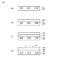
図1は、本発明の一実施形態に係る固体撮像素子の部分断面図である。図2及び図3は、図1に示す固体撮像素子の製造方法を工程順に説明する部分断面図である。図4は、図1の平面図である。 FIG. 1 is a partial cross-sectional view of a solid-state imaging device according to an embodiment of the present invention. 2 and 3 are partial cross-sectional views for explaining the manufacturing method of the solid-state imaging device shown in FIG. 1 in the order of steps. FIG. 4 is a plan view of FIG.
本発明の一実施形態に係る固体撮像素子は、図1に示すように、2次元的に配置された、光を電気信号に変換する機能を有する光電変換素子11を形成した半導体基板10上に、段差を有する平坦化層12、この平坦化層12上に形成された、入射光を色分解するカラーフィルター13、及びこのカラーフィルター12上に配置された複数の転写レンズ14により構成されている。
As shown in FIG. 1, a solid-state imaging device according to an embodiment of the present invention is two-dimensionally arranged on a
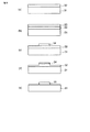
このような固体撮像素子は、図2及び図3に示す方法によって製造することが出来る。 Such a solid-state imaging device can be manufactured by the method shown in FIGS.
まず、2次元的に配置された光電変換素子21を有する半導体基板20(図2(a)参照)上に、図2(b)に示すように、第1の平坦化層22を形成する。第1の平坦化層としては、アクリル系、エポキシ系、ポリイミド系、フェノールノボラック系、ポリエステル系、ウレタン系、メラミン系、尿素系、スチレン系などの樹脂を一つもしくは複数含んだ樹脂を用いることができる。
First, as shown in FIG. 2B, the
次いで、図2(c)に示すように、第1の平坦化層22上に、緑レジスト層23を形成する。緑レジスト層23は、熱硬化性樹脂を主成分とし、緑色顔料を分散させた樹脂分散液を平坦化層22上に塗布し、熱硬化することにより形成される。
Next, as shown in FIG. 2C, a green resist
次に、この緑レジスト層22上に、例えばフォトリソグラフィーにより、図2(d)に示すように、所定の樹脂パターン24を形成する。樹脂パターン24としては、例えば、アクリル系、エポキシ系、ポリイミド系、フェノールノボラック系、その他の感光性を有する樹脂を単独でもしくは複数混合あるいは共重合して用いることができる。感光性樹脂をパターニングするフォトリソグラフィープロセスに用いる露光機は、ステッパー、アライナー、ミラープロジェクションアライナーなどがあるが、高画素化、微細化の必要な固体撮像素子のカラーフィルターを形成するにあたっては通常ステッパーを用いるのが一般的である。
Next, a
その後、この樹脂パターン24をマスクとして用いて、ドライエッチングにより緑レジスト層23をパターニングし、図3(a)に示すように、グリーンフィルターパターン25aを形成する。ドライエッチングとしては、例えば、ECR、平行平板マグネトロン、DRM、ICP、あるいは2周波タイプのRIEなどを用いることが出来る。
Thereafter, using this
ドライエッチングに用いるガスは、反応性(酸化性・還元性)のある、即ちエッチング性のあるガスであれば、よく、例えば、フッ素、塩素、臭素などのハロゲン元素をその構成に有するガス、同様に酸素やイオウの元素をその構成に有するガスなどを用いることが出来るが、これらには限定されない。 The gas used for dry etching may be a reactive (oxidative / reducing) gas, that is, an etching gas, for example, a gas having a halogen element such as fluorine, chlorine, bromine, etc. In addition, a gas having an oxygen or sulfur element in its structure can be used, but it is not limited thereto.
その後、フォトリソグラフィーにより、ブルーフィルターパターン25b及びレッドフィルターパターン(図示せず)を形成し、図3(b)に示すように、緑、青及び赤のフィルターパターンからなるカラーフィルター26を形成する。
Thereafter, a
カラーフィルター26の各色フィルターパターンの配列を示す平面図を図4に示す。図4に示す配列は、一画素おきにG(緑)フィルターが設けられ、Gフィルターの間に一行おきにR(赤)フィルターとB(青)フィルターが設けられた、いわゆるベイヤー配列である。図4におけるA−A’での断面図が図1となる。
FIG. 4 is a plan view showing the arrangement of each color filter pattern of the
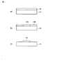
次いで、図3(c)に示すように、以上のようにして形成されたカラーフィルター26上に第2の平坦化層27を形成する。第2の平坦化層としては、第1の平坦化層と同様、アクリル系、エポキシ系、ポリイミド系、フェノールノボラック系、ポリエステル系、ウレタン系、メラミン系、尿素系、スチレン系などの樹脂を一つもしくは複数含んだ樹脂を用いることができる。
Next, as shown in FIG. 3C, a
次に、図3(d)に示すように、第2の平坦化層27上に、周知の技術である熱フロー法によりレンズ母型28を形成する。レンズ母型28としては、感光性樹脂が好ましく、アクリル樹脂やフェノール樹脂、ポリスチレン樹脂などのアルカリ可溶性および熱フロー性を有する樹脂を用いることが出来る。
Next, as shown in FIG. 3D, a
最後に、レンズ母型28をマスクとして用いてエッチング処理を行い、レンズ母型28の形状を第2の平坦化層27に転写して、マイクロレンズ29を形成する。このとき、カラーフィルター26の各パターンの境界部分表面から0.03μm〜0.5μmの深さに除去し、図3(e)に示すように、固体撮像素子が完成する。
Finally, an etching process is performed using the
以上説明した固体撮像素子の製造方法において、グリーンフィルターパターン25aは、緑レジスト層23を完全に熱硬化させた後に、ドライエッチングによりパターニングすることにより形成されているため、後のフォトリソグラフィーにおける現像工程において、画素欠損が生ずることはない。
In the manufacturing method of the solid-state imaging device described above, the
以上説明した実施形態において、グリーンフィルターパターン25aは、最も面積の大きいものとすることが望ましい。そうすることにより、下地との密着性をより強固にすることが出来、画素欠損をより効果的に防止することができる。最も面積の大きいグリーンフィルターパターンの面積は、例えば、最も面積の小さい色フィルターパターンの面積の1〜2倍とすることが出来る。また、最も面積の大きい色フィルターパターンをドライエッチングによりパターニングする形成工法で形成することで、最も広い面積を占める色フィルターパターンを正確にパターニングすることができ、カラーフィルター全体の精度向上となる。具体的にはグリーンフィルターパターンが最も大きい面積である場合が多い。
In the embodiment described above, it is desirable that the
また、顔料濃度が高い、すなわち、硬化に関与する樹脂の含有率が小さい色フィルター層をドライエッチングによりパターニングする形成工法でパターン形成することで、通常のフォトリソグラフィープロセスでは硬化不充分になってしまう色フィルター層であっても、精度良く、残渣や剥がれもなく、形成することができる。具体的にはレッドフィルターパターンあるいはグリーンフィルターパターンの場合にこの効果がある。 In addition, by forming a color filter layer with a high pigment concentration, i.e., a low content of resin involved in curing, by patterning by a dry etching method, curing is insufficient in a normal photolithography process. Even a color filter layer can be formed with high accuracy and no residue or peeling. Specifically, this effect is obtained in the case of a red filter pattern or a green filter pattern.
あるいは、フォトリソグラフィーによるパターニングに用いる露光波長の透過率が低いために露光不充分となり、解像度の低下や剥がれが起きる色フィルター層を、ドライエッチングによりパターニングする形成工法でパターン形成することで、やはり、通常のフォトリソグラフィープロセスでは硬化不充分になってしまう色フィルター層であっても、精度良く、残渣や剥がれもなく、形成することができる。特にはブルーフィルターパターンの場合にこの効果がある。 Alternatively, by forming a color filter layer by patterning by dry etching, the color filter layer that is insufficiently exposed due to the low transmittance of the exposure wavelength used for patterning by photolithography, resulting in a decrease in resolution and peeling, Even a color filter layer that is insufficiently cured by a normal photolithography process can be formed with high accuracy and without residue or peeling. This effect is particularly effective in the case of a blue filter pattern.
いずれの理由によっても、最初のパターンをドライエッチングの形成工法で形成すれば、下層の基板に密着し、残渣や剥がれがなく、また解像度の高い色フィルターパターンとなり、次いで工程が少なく効率のよいフォトリソグラフィーの形成工法で次の色フィルターパターンを形成すれば、最初に形成した色フィルターパターンが、正確なパターンで、かつ強固に基板に密着しているため、フォトリソグラフィーの形成工法であっても、正確に、剥がれのない色フィルターパターンを形成することができる。 For any reason, if the first pattern is formed by the dry etching method, it adheres to the underlying substrate, has no residue or peeling, and has a high-resolution color filter pattern. If the next color filter pattern is formed by the lithography forming method, the first formed color filter pattern is an accurate pattern and firmly adhered to the substrate, so even if it is a photolithography forming method, It is possible to accurately form a color filter pattern without peeling.
連続してドライエッチングの形成工法で色フィルターパターンを形成すると、最初に形成した色フィルターパターンの凹凸が、後から形成する色フィルター層にひびくという問題があるため、3色からなるカラーフィルターの場合は最初の1色、4色からなるカラーフィルターの場合は最初の1色または最初と2色目までをドライエッチングの工法により、残りの色はフォトリソグラフィーの工法によりパターニングすることが好ましい。 In the case of a color filter consisting of three colors, there is a problem that when the color filter pattern is continuously formed by the dry etching forming method, the unevenness of the color filter pattern formed first cracks in the color filter layer to be formed later. In the case of a color filter comprising the first one color and four colors, it is preferable that the first color or the first and second colors are patterned by a dry etching method, and the remaining colors are patterned by a photolithography method.
また、グリーンフィルターパターンに含まれる樹脂を、青及び赤のフィルターパターンに含まれる樹脂よりも高い屈折率を有するものとすることが出来る。従来、グリーンフィルターパターンの屈折率は、他のフィルターパターンの屈折率より低いため、カラーフィルターの反射率が不均一であるという問題があった。グリーンフィルターパターンの屈折率を高くするには屈折率の高い樹脂を用いればよいが、フォトリソグラフィーに供されるという制約のため、樹脂の選択の幅が狭く、屈折率の高い樹脂を選択することは困難であった。 Moreover, the resin contained in the green filter pattern can have a higher refractive index than the resin contained in the blue and red filter patterns. Conventionally, since the refractive index of the green filter pattern is lower than the refractive index of other filter patterns, there is a problem that the reflectance of the color filter is not uniform. In order to increase the refractive index of the green filter pattern, a resin having a high refractive index may be used. However, because of the limitation of being used for photolithography, a resin having a narrow selection range and a resin having a high refractive index should be selected. Was difficult.
これに対し、本実施形態では、グリーンフィルターパターンを、フォトリソグラフィーに依らずに、ドライエッチングにより形成しているため、グリーンフィルターパターンの樹脂として、熱硬化性樹脂の中から屈折率の高いものを広く選択することが可能である。 On the other hand, in this embodiment, since the green filter pattern is formed by dry etching without depending on photolithography, a resin having a high refractive index among thermosetting resins is used as a resin for the green filter pattern. A wide selection is possible.
このように、グリーンフィルターパターンに含まれる樹脂を、青及び赤のフィルターパターンに含まれる樹脂よりも高い屈折率を有するものとすることにより、3色のフィルターパターンの屈折率を近似させることが出来、それによってマイクロレンズによる集光効果を同等に出来るため、良好な固体撮像素子を得ることが出来る。 In this way, the refractive index of the three-color filter pattern can be approximated by making the resin contained in the green filter pattern have a higher refractive index than the resin contained in the blue and red filter patterns. As a result, the light condensing effect by the microlens can be made equal, so that a good solid-state imaging device can be obtained.
さらに、屈折率が高い樹脂はエッチングレートが小さい傾向にあることから、屈折率が高い樹脂を添加した層をドライエッチングでパターニングすることで、表面のなめらかな色フィルターパターンを得ることが出来る。 Furthermore, since a resin having a high refractive index tends to have a low etching rate, a smooth color filter pattern can be obtained by patterning a layer to which a resin having a high refractive index is added by dry etching.
本発明のグリーンフィルターパターンには、色フィルターパターンとなった場合に同等の屈折率を得られることから、ブルー及びレッドフィルターパターンに含まれる樹脂の屈折率よりも、0.05〜0.2程度高い屈折率を有する樹脂が好ましく用いられる。 Since the green filter pattern of the present invention can obtain the same refractive index when it becomes a color filter pattern, it is about 0.05 to 0.2 than the refractive index of the resin contained in the blue and red filter patterns. A resin having a high refractive index is preferably used.
なお、ブルー及びレッドのフィルターパターンに含まれる樹脂として、1.5〜1.6の屈折率を有するアクリル系、エポキシ系、ポリイミド系、フェノールノボラック系、ポリエステル系、ウレタン系、メラミン系、尿素系、スチレン系等の樹脂を用い、グリーンフィルターパターンに含まれる樹脂として、1.55〜1.7の屈折率を有するアクリル系、エポキシ系、ポリイミド系、フェノールノボラック系、ポリエステル系、ウレタン系、メラミン系、尿素系、スチレン系及びこれらの共重合物などの樹脂を一つもしくは複数含んだ樹脂を用いることが出来る。特に、高屈折率を達成するためにはフェノール樹脂やポリスチレン樹脂あるいはベンゼン環や芳香族環を導入したポリマーやモノマーを用いることや、ハロゲン基やイオウ原子を有する基などを骨格に導入したアクリル樹脂を用いることができる。 In addition, as resin contained in the filter pattern of blue and red, acrylic, epoxy, polyimide, phenol novolac, polyester, urethane, melamine, urea having a refractive index of 1.5 to 1.6 As a resin contained in the green filter pattern, an acrylic, epoxy, polyimide, phenol novolac, polyester, urethane, melamine having a refractive index of 1.55 to 1.7 is used. Resins containing one or more resins such as those based on urea, urea, styrene, and copolymers thereof can be used. In particular, in order to achieve a high refractive index, a phenol resin, a polystyrene resin, or a polymer or monomer having a benzene ring or aromatic ring introduced, or an acrylic resin having a halogen group or a group having a sulfur atom introduced into the skeleton Can be used.
また、マイクロレンズ形成工程において、図3(e)に示すように、隣接するフィルターパターンの境界部分を表面から0.03μm〜0.5μmの深さに除去し、マイクロレンズの周辺部をカラーフィルター26の一部により構成しているので、マイクロレンズ下距離を小さくすることができ、感度が良好な固体撮像素子を得ることが出来る。 Further, in the microlens formation step, as shown in FIG. 3E, the boundary portion between adjacent filter patterns is removed from the surface to a depth of 0.03 μm to 0.5 μm, and the peripheral portion of the microlens is a color filter. 26, the distance below the microlens can be reduced, and a solid-state imaging device with good sensitivity can be obtained.
ここで、隣接するフィルターパターンの境界部分の除去する深さの下限を0.03μmとしたのは、SEMやAFMなどで実効的に膜厚を識別することが出来る最小の値であるためであり、また、上限を0.5μmとしたのは、0.5μmを越えると、膜表面が荒れて、表面散乱による感度低下が生ずるためである。更に、0.5μmを越えると、実効的なカラーフィルターの膜厚が、例えば1μm以上に厚くなることがあり、本発明の課題の一つである薄膜化からはずれてしまうからである。 Here, the reason why the lower limit of the depth to be removed at the boundary portion between adjacent filter patterns is set to 0.03 μm is that it is the minimum value that can effectively identify the film thickness by SEM or AFM. The reason why the upper limit is set to 0.5 μm is that when the thickness exceeds 0.5 μm, the film surface becomes rough and the sensitivity is lowered due to surface scattering. Further, if it exceeds 0.5 μm, the effective color filter film thickness may be increased to, for example, 1 μm or more, and the film thickness is not one of the problems of the present invention.
以下、本発明の実施例を示し、本発明をより具体的に説明する。 Hereinafter, the present invention will be described more specifically by showing examples of the present invention.
実施例1
図2及び図3を参照して、本実施例に係る固体撮像素子の製造方法について説明する。
Example 1
With reference to FIG.2 and FIG.3, the manufacturing method of the solid-state image sensor which concerns on a present Example is demonstrated.
図2(a)に示すような、2次元的に配置された光電変換素子21を備える半導体基板20上に、アクリル系樹脂を主成分とする塗布液を2000rpmの回転数でスピンコートした後、ホットプレートにより230℃で6分間ベークし、図2(b)に示すように、第1の平坦化層22を形成した。この時の第1の平坦化層22の膜厚は0.45μmであった。
After spin-coating a coating liquid mainly composed of an acrylic resin at a rotational speed of 2000 rpm on a
次いで、第1の平坦化層22の上に、顔料分散グリーンレジストを1000rpmの回転数でスピンコートした後、230℃で6分間ベークし、図2(c)に示すように、グリーンレジスト層23を形成した。この時、グリーンの顔料にはカラーインデックスにてC.I.PG36を用いており、その顔料濃度は35重量%、膜厚は0.5μmである。また、グリーンレジストの主成分である樹脂としては、熱硬化タイプのアクリル系高屈折率樹脂を用いた。そのため、グリーンレジスト層23の屈折率は1.65である。
Next, a pigment-dispersed green resist is spin-coated on the
このように、熱硬化タイプのアクリル系高屈折率樹脂を用いることにより、熱硬化剤が必要になるものの、光重合開始剤などの感剤を無くすことが出来るとともに、アルカリ現像特性や光硬化性などのフォトリソグラフィー特性が必要でないため、顔料濃度を上げることによりグリーンフィルターの薄膜化を達成することが出来た。 As described above, by using a thermosetting acrylic high refractive index resin, a thermosetting agent is required, but a photopolymerization initiator and other sensitizers can be eliminated, and alkali development characteristics and photocuring properties can be eliminated. Since the photolithography characteristics such as the above are not necessary, the green filter can be made thinner by increasing the pigment concentration.
次に、グリーンレジスト層23上に、アクリル系感光樹脂を主成分とする塗布液を3000rpmの回転数でスピンコートした後、フォトリソグラフィーによりパターニングし、図2(d)に示すように、透明樹脂パターン24を形成した。このとき、マスクとなる透明樹脂には顔料などの解像性の妨げとなる物質が含まれないものを選択できることから、高精細でパターニングできる。
Next, a coating solution mainly composed of an acrylic photosensitive resin is spin-coated on the green resist
その後、この透明樹脂パターン24をマスクとして用いて、ドライエッチング装置にてフロン系ガスを用いてグリーンレジスト層23をエッチング処理し、図3(a)に示すように、グリーンフィルターパターン25aを形成した。このときのグリーンフィルターパターン25aの膜厚は0.5μmであり、第1の平坦化層22も一部除去されたため、隣接する第1の平坦化層22との間には0.4μmの段差が形成されていた。
Thereafter, using the
その後、フォトリソグラフィーにより、図3(b)に示すように、ブルーフィルターパターン25b及びレッドフィルターパターン(図示せず)を順次形成し、カラーフィルター26を得た。この時、ブルーレジストに用いた顔料は、それぞれカラーインデックスにてC.I.PB15:6、C.I.PV23であり、顔料濃度は30重量%、膜厚は0.9μm、屈折率は1.64であり、レッドレジストに用いた顔料は、それぞれカラーインデックスにてC.I.PR117、C.I.PR48:1、C.I.PY139であり、顔料濃度は40重量%、膜厚は0.9μm、屈折率は1.69であった。
Thereafter, as shown in FIG. 3B, a
更に、このようにして形成されたカラーフィルター26上に、UV吸収剤を添加したアクリル樹脂を含む塗布液を回転数1000rpmでスピンコートし、ホットプレートにて200℃で10分間の熱処理を施して、樹脂を硬化し、図3(c)に示すように、第2の平坦化層27を形成した。
Further, on the
次に、図3(d)に示すように、平坦化層27上に、周知の技術である熱フロー法により感光性、熱フロー性のあるアクリル樹脂からなるレンズ母型28を形成した。
Next, as shown in FIG. 3D, a
最後に、ドライエッチング装置にて、フロン系ガスを用いてレンズ母型28をマスクとして用いてエッチング処理を行い、レンズ母型28の形状を第2の平坦化層27に転写して、マイクロレンズ29を形成した。このとき、カラーフィルター26の各パターンの境界部分表面から0.2μmの深さに除去し、図3(e)に示すように、固体撮像素子を完成した。
Finally, in a dry etching apparatus, an etching process is performed by using a fluorocarbon gas using the
以上のような固体撮像素子の製造方法では、グリーンフィルターパターン25aをドライエッチングによるパターン形成工法を用いて形成することにより、微細なパターンの膜厚の薄いカラーフィルターを、良好な形状で残渣なしに、画素剥がれを生ずることなく形成することが出来た。また、グリーンフィルター層に熱硬化性樹脂を用いたため、固形分中の色材の濃度を上げることが出来るので、カラーフィルターを薄く形成することが出来、薄型の固体撮像素子を得ることが出来た。
In the manufacturing method of the solid-state imaging device as described above, the
本実施例においては、ドライエッチングによる形状転写技術で形成したグリーンレジスト及びブルーレジストの主成分として熱硬化タイプのアクリル樹脂を用いたが、特にアクリル樹脂にこだわることなく、エポキシ樹脂、ポリイミド樹脂、フェノールノボラック樹脂、ポリエステル樹脂、ウレタン樹脂、メラミン樹脂、尿素樹脂、スチレン樹脂、及びこれらの共重合体などの樹脂の1つ叉は複数種を含む樹脂を用いることも可能である。 In this example, a thermosetting acrylic resin was used as the main component of the green resist and blue resist formed by the shape transfer technique by dry etching, but epoxy resin, polyimide resin, phenol, and the like were not particularly concerned with acrylic resin. It is also possible to use a resin including one or more kinds of resins such as a novolac resin, a polyester resin, a urethane resin, a melamine resin, a urea resin, a styrene resin, and a copolymer thereof.
特に、高屈折率を達成するために、フェノール樹脂やポリスチレン樹脂あるいはベンゼン環や芳香環を導入したポリマーやモノマーを用いること、及びハロゲン基やイオウ基などをこれらポリマーなどの骨格に導入したアクリル樹脂を用いることが可能である。 In particular, in order to achieve a high refractive index, a phenol resin, a polystyrene resin, or a polymer or monomer into which a benzene ring or an aromatic ring is introduced, and an acrylic resin in which a halogen group or a sulfur group is introduced into the skeleton of these polymers, etc. Can be used.
これにより、従来、ブルーフィルターパターンやレッドフィルターパターンと比較して最も屈折率が低く、表面反射が大きいグリーンフィルターパターンにおいても、高い屈折率を達成することができ、感度の良好な固体撮像素子を得ることが出来る。 This makes it possible to achieve a high refractive index even in a green filter pattern that has the lowest refractive index and a large surface reflection compared to the blue filter pattern and the red filter pattern, and has a good sensitivity. Can be obtained.
また、以上の実施例では、グリーンフィルターパターンをドライエッチングを用いたパターニングにより形成したが、フォトリソグラフィープロセスによって剥がれの生じやすいブルーフィルターパターンや顔料濃度の高いレッドフィルターパターンをドライエッチングを用いて形成しても構わない。ただし、1色目となるグリーンフィルターパターンの密着性とパターン精度が最も重要であるため、グリーンフィルターパターンをドライエッチング技術による形状転写技術で形成することが必要である。また、グリーンフィルターパターンを形成した後の2色目としてレッドフィルターパターンを形成してもよいが、レッドフィルターパターンは顔料濃度が高いため、残渣が残りやすいので、ブルーフィルターパターンを2色目として形成するのが望ましい。 In the above embodiments, the green filter pattern is formed by patterning using dry etching. However, a blue filter pattern or a red filter pattern having a high pigment concentration that is easily peeled off by a photolithography process is formed by dry etching. It doesn't matter. However, since the adhesion and pattern accuracy of the first color green filter pattern are the most important, it is necessary to form the green filter pattern by a shape transfer technique using a dry etching technique. In addition, a red filter pattern may be formed as the second color after the green filter pattern is formed. However, since the red filter pattern has a high pigment concentration, residue is likely to remain, so the blue filter pattern is formed as the second color. Is desirable.
また、本実施例においては、カラーフィルター26の下部に配設される第1の平坦化層22に0.4μmの段差を設けたが、グリーンフィルターパターン形成の母型となる透明樹脂パターン24の厚みや材料の選択によるエッチングレートの調整により、0.03μm〜0.5μmの範囲内で第1の平坦化層をエッチングしても構わない。ここで、下限を0.03μmとしたのは、SEMやAFMなどで実効的に膜厚を識別出来る最小の値であるためであり、また上限を0.5μmとしたのは、0.5μmを越える段差をつけると、膜表面があれ、表面散乱による感度低下が生ずるためである。
In the present embodiment, a step of 0.4 μm is provided in the
更に、本実施例においては、ドライエッチングによりマイクロレンズを形成したが、従来の熱フロー法によりマイクロレンズを形成してもよい。ただし、マイクロレンズ下の厚みを薄くするためには、ドライエッチングによる形状転写技術を用いてマイクロレンズを形成する方がより好ましい。 Further, in this embodiment, the microlens is formed by dry etching, but the microlens may be formed by a conventional heat flow method. However, in order to reduce the thickness under the microlens, it is more preferable to form the microlens using a shape transfer technique by dry etching.
実施例2
図2及び図5を参照して、本実施例に係る固体撮像素子の製造方法について説明する。
Example 2
With reference to FIG.2 and FIG.5, the manufacturing method of the solid-state image sensor which concerns on a present Example is demonstrated.
図2(a)に示すような、2次元的に配置された光電変換素子21を備える半導体基板20上に、アクリル系樹脂を主成分とする塗布液を2000rpmの回転数でスピンコートした後、ホットプレートにより230℃で6分間ベークし、図2(b)に示すように、第1の平坦化層22を形成した。この時の第1の平坦化層22の膜厚は0.4μmであった。
After spin-coating a coating liquid mainly composed of an acrylic resin at a rotational speed of 2000 rpm on a
次いで、第1の平坦化層22の上に、顔料分散グリーンレジストを1000rpmの回転数でスピンコートした後、230℃で6分間ベークし、図2(c)に示すように、グリーンレジスト層23を形成した。この時、グリーンの顔料にはカラーインデックスにてC.I.PG36を用いており、その顔料濃度は40重量%、膜厚は0.5μmである。また、グリーンレジストの主成分である樹脂としては、熱硬化タイプのアクリル系高屈折率樹脂を用いた。そのため、グリーンレジスト層23の屈折率は1.65である。
Next, a pigment-dispersed green resist is spin-coated on the
このように、熱硬化タイプのアクリル系高屈折率樹脂を用いることにより、熱硬化剤が必要になるものの、光重合開始剤などの感剤を無くすことが出来るとともに、アルカリ現像特性や光硬化性などのフォトリソグラフィー特性が必要でないため、顔料濃度を上げることによりグリーンフィルターの薄膜化を達成することが出来た。 As described above, by using a thermosetting acrylic high refractive index resin, a thermosetting agent is required, but a photopolymerization initiator and other sensitizers can be eliminated, and alkali development characteristics and photocuring properties can be eliminated. Since the photolithography characteristics such as the above are not necessary, the green filter can be made thinner by increasing the pigment concentration.
次に、グリーンレジスト層23上に、アクリル系感光樹脂を主成分とする塗布液を3000rpmの回転数でスピンコートした後、フォトリソグラフィーによりパターニングし、図2(d)に示すように、透明樹脂パターン24を形成した。このとき、マスクとなる透明樹脂には顔料などの解像性の妨げとなる物質が含まれないものを選択できることから、高精細でパターニングできる。
Next, a coating solution mainly composed of an acrylic photosensitive resin is spin-coated on the green resist
その後、この透明樹脂パターン24をマスクとして用いて、ドライエッチング装置にてフロン系ガスを用いてグリーンレジスト層23をエッチング処理し、図5(a)に示すように、グリーンフィルターパターン25aを形成した。このときのグリーンフィルターパターン25aの膜厚は0.5μmであり、グリーンフィルターパターン25aで覆われていない第1の平坦化層22は完全に除去されていた。
Thereafter, using the
その後、フォトリソグラフィーにより、図5(b)に示すように、ブルーフィルターパターン25b及びレッドフィルターパターン(図示せず)を順次形成し、カラーフィルター26を得た。この時、ブルーレジストに用いた顔料は、それぞれカラーインデックスにてC.I.PB15:6、C.I.PV23であり、顔料濃度は30重量%、膜厚は0.9μm、屈折率は1.64であり、レッドレジストに用いた顔料は、それぞれカラーインデックスにてC.I.PR117、C.I.PR48:1、C.I.PY139であり、顔料濃度は40重量%、膜厚は0.9μm、屈折率は1.69であった。
Thereafter, as shown in FIG. 5B, a
更に、このようにして形成されたカラーフィルター26上に、UV吸収剤を添加したアクリル樹脂を含む塗布液を回転数1000rpmでスピンコートし、ホットプレートにて200℃で10分間の熱処理を施して、樹脂を硬化し、図5(c)に示すように、第2の平坦化層27を形成した。
Further, on the
次に、図5(d)に示すように、平坦化層27上に、周知の技術である熱フロー法により感光性、熱フロー性のあるアクリル樹脂からなるレンズ母型28を形成した。
Next, as shown in FIG. 5D, a
最後に、ドライエッチング装置にて、フロン系ガスを用いてレンズ母型28をマスクとして用いてエッチング処理を行い、レンズ母型28の形状を第2の平坦化層27に転写して、マイクロレンズ29を形成した。このとき、カラーフィルター26の各パターンの境界部分表面から0.1μmの深さに除去し、図5(e)に示すように、固体撮像素子を完成した。
Finally, in a dry etching apparatus, an etching process is performed by using a fluorocarbon gas using the
以上のような固体撮像素子の製造方法では、グリーンフィルターパターン25aをドライエッチングによるパターン形成工法を用いて形成することにより、微細なパターンの膜厚の薄いカラーフィルターを、良好な形状で残渣なしに、画素剥がれを生ずることなく形成することが出来た。また、グリーンフィルタ層に熱硬化性樹脂を用いたため、固形分中の色材の濃度を上げることが出来るので、カラーフィルターを薄く形成することが出来、薄型の固体撮像素子を得ることが出来た。
In the manufacturing method of the solid-state imaging device as described above, the
また、本実施例においては、フォトリソグラフィーによるパターン形成工法で形成される色フィルターパターンの下部に配設される第1の平坦化層22を完全に取り除いたが、グリーンフィルターパターン形成の母型となる透明樹脂パターン24の厚みや材料の選択によるエッチングレートの調整により、第1の平坦化層を残しても構わない。ただし、2色目以降の色フィルター層の残渣を残さないようにするためには、完全に除去することが好ましい。
Further, in this embodiment, the
更に、本実施例においては、ドライエッチングによりマイクロレンズを形成したが、従来の熱フロー法によりマイクロレンズを形成してもよい。ただし、マイクロレンズ下の厚みを薄くするためには、ドライエッチングによる形状転写技術を用いてマイクロレンズを形成する方がより好ましい。 Further, in this embodiment, the microlens is formed by dry etching, but the microlens may be formed by a conventional heat flow method. However, in order to reduce the thickness under the microlens, it is more preferable to form the microlens using a shape transfer technique by dry etching.
また、隣接するカラーフィルターの境界部分を表面から0.1μmの深さでエッチングし、マイクロレンズの周辺部をカラーフィルターの一部で構成されるようにしたが、レンズ母型の高さや材料の選択、またレンズ形状を転写される層の層構成、厚みやエッチングレート等から材料を選択することにより、表面から0.03μmから0.5μmの範囲で除去する深さを設定することができる。ここで、下限を0.03μmとしたのはSEMやAFMなどで膜厚を識別できる最小の値であるためであり、また上限を0.5μmとしたのはこれ以上深くドライエッチングを行うと、マイクロレンズ表面が荒れて、表面散乱により感度低下が起こるためである。 In addition, the boundary part of adjacent color filters was etched at a depth of 0.1 μm from the surface, and the peripheral part of the microlens was made up of part of the color filter. The depth to be removed in the range of 0.03 μm to 0.5 μm from the surface can be set by selecting the material from the selection, the layer configuration of the layer to which the lens shape is transferred, the thickness, the etching rate, and the like. Here, the lower limit is set to 0.03 μm because it is the minimum value that can identify the film thickness by SEM or AFM, and the upper limit is set to 0.5 μm when dry etching is performed deeper than this. This is because the surface of the microlens is rough and the sensitivity is lowered due to surface scattering.
10,20…半導体基板、11,21…光電変換素子、12…平坦化層、13,26…カラーフィルター、14,29…マイクロレンズ、22…第1の平坦化層、23…緑レジスト層、24…樹脂パターン、25a…グリーンフィルターパターン、25b・・ブルーフィルターパターン、27…第2の平坦化層、28…レンズ母型、31,41…基材、32,42…色フィルター層、33…感光性樹脂層、34…樹脂パターン、35,43…色フィルターパターン、42a…光硬化部、42b…不要部。
DESCRIPTION OF
Claims (13)
前記複数色の色フィルターパターンは、所定の色フィルター層をドライエッチングによりパターニングする形成工法と、他の色フィルター層をフォトリソグラフィーによりパターニングする形成工法とによって形成され、
前記複数色の色フィルターパターンのうち少なくとも最初に形成される色フィルターパターンを、色フィルター層の不要部とその下層の平坦化層をドライエッチングすることにより形成する工程、及び
他の色フィルターパターンをフォトリソグラフィーによりパターニングして形成する工程を有し、
前記ドライエッチングにより形成された色フィルターパターンと前記フォトリソグラフィーにより形成された他の色フィルターパターンとが接していることを特徴とする固体撮像素子の製造方法。 Two-dimensionally arranged photoelectric conversion elements on a semiconductor substrate, a color filter having a plurality of color filter patterns disposed on the semiconductor substrate corresponding to each of the photoelectric conversion elements, and the semiconductor substrate A method for producing a solid-state imaging device comprising a planarization layer formed on a part or all of the above,
The plurality of color filter patterns are formed by a forming method of patterning a predetermined color filter layer by dry etching and a forming method of patterning another color filter layer by photolithography,
Forming a color filter pattern formed at least first among the color filter patterns of the plurality of colors by dry-etching an unnecessary portion of the color filter layer and a flattening layer below the color filter layer; and other color filter patterns Having a process of patterning by photolithography ,
A method of manufacturing a solid-state imaging device, wherein a color filter pattern formed by the dry etching is in contact with another color filter pattern formed by the photolithography .
前記複数色の色フィルターパターン下の平坦化層は、ドライエッチングによって形成されたある色フィルターパターンと、前記ドライエッチングによってある色フィルターパターンを形成した後にフォトリソグラフィーによって形成された他の色フィルターパターンとの間で厚みが異なり、
前記ドライエッチングにより形成された色フィルターパターンと前記フォトリソグラフィーにより形成された他の色フィルターパターンとが接していることを特徴とする固体撮像素子。 Two-dimensionally arranged photoelectric conversion elements on a semiconductor substrate, a color filter having a plurality of color filter patterns disposed on the semiconductor substrate corresponding to each of the photoelectric conversion elements, and the semiconductor substrate A solid-state imaging device comprising a planarization layer formed on a part or all of the above,
Said plural colors flattening layer below the color filter pattern of a certain color filter pattern formed by dry etching, and other color filter pattern formed by photolithography after forming the color filter patterns in by the dry etching Ri is Do different thickness between,
A solid-state imaging device , wherein a color filter pattern formed by the dry etching is in contact with another color filter pattern formed by the photolithography .
前記カラーフィルターは、前記半導体基板上に、平坦化層を介して形成されているドライエッチングによって形成された色フィルターパターンと、直接形成されている、前記ドライエッチングによって色フィルターパターンを形成した後にフォトリソグラフィーによって形成された他の色フィルターパターンの両方を有するカラーフィルタであり、
前記ドライエッチングにより形成された色フィルターパターンと前記フォトリソグラフィーにより形成された他の色フィルターパターンとが接していることを特徴とする固体撮像素子。 Two-dimensionally arranged photoelectric conversion elements on a semiconductor substrate, a color filter having a plurality of color filter patterns disposed on the semiconductor substrate corresponding to each of the photoelectric conversion elements, and the semiconductor substrate A solid-state imaging device comprising a planarization layer formed on a part or all of the above,
The color filter includes a color filter pattern formed by dry etching formed on the semiconductor substrate through a planarization layer, and a color filter pattern formed directly by the dry etching, and then a photo filter. the color filter der with both other color filter pattern formed by lithography is,
A solid-state imaging device , wherein a color filter pattern formed by the dry etching is in contact with another color filter pattern formed by the photolithography .
前記複数色の色フィルターパターンのうち一部の色フィルターパターンは熱硬化性を有する樹脂を含み、前記熱硬化性を有する樹脂を含む色フィルターパターンを形成した後に形成された残りの色フィルターパターンは光硬化性を有する樹脂を含み、
前記熱硬化性を有する樹脂を含む色フィルターパターンと前記光硬化性を有する樹脂を含む色フィルターパターンとが接していることを特徴とする固体撮像素子。 Two-dimensionally arranged photoelectric conversion elements on a semiconductor substrate, a color filter having a plurality of color filter patterns disposed on the semiconductor substrate corresponding to each of the photoelectric conversion elements, and the semiconductor substrate A solid-state imaging device comprising a planarization layer formed on a part or all of the above,
Among the plurality of color filter patterns, some of the color filter patterns include a thermosetting resin, and the remaining color filter patterns formed after forming the color filter pattern including the thermosetting resin are: a resin having a photocurable seen including,
A solid-state imaging device , wherein the color filter pattern containing the thermosetting resin is in contact with the color filter pattern containing the photocurable resin .
Priority Applications (7)
| Application Number | Priority Date | Filing Date | Title |
|---|---|---|---|
| JP2005034621A JP4984400B2 (en) | 2005-02-10 | 2005-02-10 | Solid-state imaging device and manufacturing method thereof |
| KR1020077017581A KR100934513B1 (en) | 2005-02-10 | 2006-02-07 | Solid-state image sensor and its manufacturing method |
| EP06713204.3A EP1855320B1 (en) | 2005-02-10 | 2006-02-07 | Solid-state imaging device and method for manufacturing same |
| PCT/JP2006/302061 WO2006085528A1 (en) | 2005-02-10 | 2006-02-07 | Solid-state imaging device and method for manufacturing same |
| TW095104297A TWI316636B (en) | 2005-02-10 | 2006-02-09 | Solid-state image pick-up device |
| US11/889,070 US8097485B2 (en) | 2005-02-10 | 2007-08-08 | Solid state image pickup device and manufacturing method thereof |
| US12/662,368 US7932122B2 (en) | 2005-02-10 | 2010-04-13 | Manufacturing method for solid state image pickup device |
Applications Claiming Priority (1)
| Application Number | Priority Date | Filing Date | Title |
|---|---|---|---|
| JP2005034621A JP4984400B2 (en) | 2005-02-10 | 2005-02-10 | Solid-state imaging device and manufacturing method thereof |
Publications (2)
| Publication Number | Publication Date |
|---|---|
| JP2006222291A JP2006222291A (en) | 2006-08-24 |
| JP4984400B2 true JP4984400B2 (en) | 2012-07-25 |
Family
ID=36984379
Family Applications (1)
| Application Number | Title | Priority Date | Filing Date |
|---|---|---|---|
| JP2005034621A Expired - Fee Related JP4984400B2 (en) | 2005-02-10 | 2005-02-10 | Solid-state imaging device and manufacturing method thereof |
Country Status (1)
| Country | Link |
|---|---|
| JP (1) | JP4984400B2 (en) |
Families Citing this family (7)
| Publication number | Priority date | Publication date | Assignee | Title |
|---|---|---|---|---|
| JP2008159748A (en) * | 2006-12-22 | 2008-07-10 | Toppan Printing Co Ltd | Method for manufacturing solid-state image sensing device and solid-state image sensing device |
| JP2014164070A (en) * | 2013-02-25 | 2014-09-08 | Seiko Epson Corp | Color filter substrate, electro-optic device, method for manufacturing electro-optic device and electronic equipment |
| KR102626698B1 (en) * | 2015-11-16 | 2024-01-19 | 도판 인사츠 가부시키가이샤 | Manufacturing method of solid-state imaging device, solid-state imaging device, and manufacturing method of color filter and color filter |
| KR102471568B1 (en) | 2016-12-27 | 2022-11-29 | 도판 인사츠 가부시키가이샤 | Solid-state imaging device and manufacturing method therefor |
| JP6838394B2 (en) * | 2016-12-27 | 2021-03-03 | 凸版印刷株式会社 | Solid-state image sensor and its manufacturing method |
| JP6809215B2 (en) * | 2016-12-27 | 2021-01-06 | 凸版印刷株式会社 | Solid-state image sensor and its manufacturing method |
| JP2019087545A (en) * | 2017-11-01 | 2019-06-06 | 凸版印刷株式会社 | Solid-state image sensor and method of manufacturing the same |
Family Cites Families (5)
| Publication number | Priority date | Publication date | Assignee | Title |
|---|---|---|---|---|
| JPS63188104A (en) * | 1987-01-30 | 1988-08-03 | Mitsubishi Electric Corp | Production of color filter |
| JPH0215201A (en) * | 1989-04-28 | 1990-01-18 | Hitachi Ltd | Solid-state image pickup element |
| JP3085592B2 (en) * | 1991-03-25 | 2000-09-11 | 株式会社日立製作所 | Color solid-state imaging device and method of manufacturing the same |
| JPH06289217A (en) * | 1993-04-02 | 1994-10-18 | Hitachi Ltd | Color solid state image pickup device and its production |
| JP4304987B2 (en) * | 2003-01-24 | 2009-07-29 | 凸版印刷株式会社 | Solid-state imaging device and manufacturing method thereof |
-
2005
- 2005-02-10 JP JP2005034621A patent/JP4984400B2/en not_active Expired - Fee Related
Also Published As
| Publication number | Publication date |
|---|---|
| JP2006222291A (en) | 2006-08-24 |
Similar Documents
| Publication | Publication Date | Title |
|---|---|---|
| JP4857569B2 (en) | Solid-state imaging device and manufacturing method thereof | |
| KR100934513B1 (en) | Solid-state image sensor and its manufacturing method | |
| TWI716490B (en) | Solid-state imaging element manufacturing method, solid-state imaging element, and color filter manufacturing method and color filter | |
| JP4984400B2 (en) | Solid-state imaging device and manufacturing method thereof | |
| JP2007281016A (en) | Color imaging element and method of manufacturing the same | |
| KR102468312B1 (en) | Solid-state imaging device and method for manufacturing the solid-state imaging device | |
| KR102471568B1 (en) | Solid-state imaging device and manufacturing method therefor | |
| TW201926730A (en) | Solid-state image capture element and method of manufacturing same | |
| JP2009152315A (en) | Image sensor and its manufacturing method | |
| JP4367078B2 (en) | Color solid-state imaging device and manufacturing method thereof | |
| JP6536005B2 (en) | Method of manufacturing color filter and color filter | |
| JP6809215B2 (en) | Solid-state image sensor and its manufacturing method | |
| JP6838394B2 (en) | Solid-state image sensor and its manufacturing method | |
| JP2016225338A (en) | Solid state imaging device | |
| JP2005311275A (en) | Solid-state imaging device and its manufacturing method | |
| TW201931615A (en) | Solid-state image capture element and method of manufacturing same | |
| TW200901451A (en) | Color photography element and method of manufacturing color photography element |
Legal Events
| Date | Code | Title | Description |
|---|---|---|---|
| A621 | Written request for application examination |
Free format text: JAPANESE INTERMEDIATE CODE: A621 Effective date: 20080124 |
|
| A131 | Notification of reasons for refusal |
Free format text: JAPANESE INTERMEDIATE CODE: A131 Effective date: 20111004 |
|
| A521 | Request for written amendment filed |
Free format text: JAPANESE INTERMEDIATE CODE: A523 Effective date: 20111205 |
|
| A131 | Notification of reasons for refusal |
Free format text: JAPANESE INTERMEDIATE CODE: A131 Effective date: 20120117 |
|
| A521 | Request for written amendment filed |
Free format text: JAPANESE INTERMEDIATE CODE: A523 Effective date: 20120314 |
|
| TRDD | Decision of grant or rejection written | ||
| A01 | Written decision to grant a patent or to grant a registration (utility model) |
Free format text: JAPANESE INTERMEDIATE CODE: A01 Effective date: 20120403 |
|
| A01 | Written decision to grant a patent or to grant a registration (utility model) |
Free format text: JAPANESE INTERMEDIATE CODE: A01 |
|
| A61 | First payment of annual fees (during grant procedure) |
Free format text: JAPANESE INTERMEDIATE CODE: A61 Effective date: 20120416 |
|
| R150 | Certificate of patent or registration of utility model |
Ref document number: 4984400 Country of ref document: JP Free format text: JAPANESE INTERMEDIATE CODE: R150 Free format text: JAPANESE INTERMEDIATE CODE: R150 |
|
| FPAY | Renewal fee payment (event date is renewal date of database) |
Free format text: PAYMENT UNTIL: 20150511 Year of fee payment: 3 |
|
| RD04 | Notification of resignation of power of attorney |
Free format text: JAPANESE INTERMEDIATE CODE: A7424 Effective date: 20120529 |
|
| A072 | Dismissal of procedure [no reply to invitation to correct request for examination] |
Free format text: JAPANESE INTERMEDIATE CODE: A072 Effective date: 20121009 |
|
| R250 | Receipt of annual fees |
Free format text: JAPANESE INTERMEDIATE CODE: R250 |
|
| R250 | Receipt of annual fees |
Free format text: JAPANESE INTERMEDIATE CODE: R250 |
|
| LAPS | Cancellation because of no payment of annual fees |