JP6300236B2 - 半導体装置、半導体装置の製造方法および電力変換装置 - Google Patents
半導体装置、半導体装置の製造方法および電力変換装置 Download PDFInfo
- Publication number
- JP6300236B2 JP6300236B2 JP2015036099A JP2015036099A JP6300236B2 JP 6300236 B2 JP6300236 B2 JP 6300236B2 JP 2015036099 A JP2015036099 A JP 2015036099A JP 2015036099 A JP2015036099 A JP 2015036099A JP 6300236 B2 JP6300236 B2 JP 6300236B2
- Authority
- JP
- Japan
- Prior art keywords
- metal layer
- semiconductor
- layer
- semiconductor device
- electrode structure
- Prior art date
- Legal status (The legal status is an assumption and is not a legal conclusion. Google has not performed a legal analysis and makes no representation as to the accuracy of the status listed.)
- Active
Links
- 239000004065 semiconductor Substances 0.000 title claims description 218
- 238000004519 manufacturing process Methods 0.000 title claims description 17
- 238000006243 chemical reaction Methods 0.000 title claims description 14
- 239000002184 metal Substances 0.000 claims description 81
- 229910052751 metal Inorganic materials 0.000 claims description 81
- 239000010949 copper Substances 0.000 claims description 59
- 239000000758 substrate Substances 0.000 claims description 44
- 239000013078 crystal Substances 0.000 claims description 43
- 229910052802 copper Inorganic materials 0.000 claims description 32
- RYGMFSIKBFXOCR-UHFFFAOYSA-N Copper Chemical compound [Cu] RYGMFSIKBFXOCR-UHFFFAOYSA-N 0.000 claims description 30
- 238000009792 diffusion process Methods 0.000 claims description 26
- 238000000034 method Methods 0.000 claims description 21
- 229910000838 Al alloy Inorganic materials 0.000 claims description 20
- 230000002265 prevention Effects 0.000 claims description 18
- 239000000463 material Substances 0.000 claims description 15
- 238000004544 sputter deposition Methods 0.000 claims description 9
- QPLDLSVMHZLSFG-UHFFFAOYSA-N Copper oxide Chemical compound [Cu]=O QPLDLSVMHZLSFG-UHFFFAOYSA-N 0.000 description 13
- 229910000789 Aluminium-silicon alloy Inorganic materials 0.000 description 10
- 229910000679 solder Inorganic materials 0.000 description 10
- 238000010586 diagram Methods 0.000 description 9
- 229960004643 cupric oxide Drugs 0.000 description 7
- 230000007547 defect Effects 0.000 description 7
- 239000012535 impurity Substances 0.000 description 7
- 230000015572 biosynthetic process Effects 0.000 description 6
- 238000007772 electroless plating Methods 0.000 description 6
- 239000002245 particle Substances 0.000 description 6
- NWONKYPBYAMBJT-UHFFFAOYSA-L zinc sulfate Chemical compound [Zn+2].[O-]S([O-])(=O)=O NWONKYPBYAMBJT-UHFFFAOYSA-L 0.000 description 6
- 230000007774 longterm Effects 0.000 description 5
- 238000000206 photolithography Methods 0.000 description 4
- 230000001681 protective effect Effects 0.000 description 4
- 230000008646 thermal stress Effects 0.000 description 4
- 229910045601 alloy Inorganic materials 0.000 description 3
- 239000000956 alloy Substances 0.000 description 3
- 239000000919 ceramic Substances 0.000 description 3
- 230000000694 effects Effects 0.000 description 3
- 238000009713 electroplating Methods 0.000 description 3
- 238000005304 joining Methods 0.000 description 3
- 238000002161 passivation Methods 0.000 description 3
- 238000007747 plating Methods 0.000 description 3
- 239000004642 Polyimide Substances 0.000 description 2
- 238000005229 chemical vapour deposition Methods 0.000 description 2
- 238000009429 electrical wiring Methods 0.000 description 2
- 229910052759 nickel Inorganic materials 0.000 description 2
- 230000003647 oxidation Effects 0.000 description 2
- 238000007254 oxidation reaction Methods 0.000 description 2
- 229920001721 polyimide Polymers 0.000 description 2
- 239000002243 precursor Substances 0.000 description 2
- 238000007790 scraping Methods 0.000 description 2
- ZOXJGFHDIHLPTG-UHFFFAOYSA-N Boron Chemical group [B] ZOXJGFHDIHLPTG-UHFFFAOYSA-N 0.000 description 1
- 239000005751 Copper oxide Substances 0.000 description 1
- 229910000881 Cu alloy Inorganic materials 0.000 description 1
- OAICVXFJPJFONN-UHFFFAOYSA-N Phosphorus Chemical compound [P] OAICVXFJPJFONN-UHFFFAOYSA-N 0.000 description 1
- ATJFFYVFTNAWJD-UHFFFAOYSA-N Tin Chemical compound [Sn] ATJFFYVFTNAWJD-UHFFFAOYSA-N 0.000 description 1
- 230000003213 activating effect Effects 0.000 description 1
- 238000000137 annealing Methods 0.000 description 1
- 229910052785 arsenic Inorganic materials 0.000 description 1
- RQNWIZPPADIBDY-UHFFFAOYSA-N arsenic atom Chemical compound [As] RQNWIZPPADIBDY-UHFFFAOYSA-N 0.000 description 1
- 230000009286 beneficial effect Effects 0.000 description 1
- 239000007767 bonding agent Substances 0.000 description 1
- 229910052796 boron Inorganic materials 0.000 description 1
- 230000015556 catabolic process Effects 0.000 description 1
- 239000003638 chemical reducing agent Substances 0.000 description 1
- 239000002131 composite material Substances 0.000 description 1
- 239000004020 conductor Substances 0.000 description 1
- 238000007796 conventional method Methods 0.000 description 1
- 229910000431 copper oxide Inorganic materials 0.000 description 1
- 238000012217 deletion Methods 0.000 description 1
- 230000037430 deletion Effects 0.000 description 1
- 238000013461 design Methods 0.000 description 1
- 230000006866 deterioration Effects 0.000 description 1
- 238000011161 development Methods 0.000 description 1
- 230000007613 environmental effect Effects 0.000 description 1
- 230000010354 integration Effects 0.000 description 1
- 238000005468 ion implantation Methods 0.000 description 1
- 238000005224 laser annealing Methods 0.000 description 1
- 239000012528 membrane Substances 0.000 description 1
- 239000002923 metal particle Substances 0.000 description 1
- 239000002105 nanoparticle Substances 0.000 description 1
- 150000002894 organic compounds Chemical class 0.000 description 1
- 229910052698 phosphorus Inorganic materials 0.000 description 1
- 239000011574 phosphorus Substances 0.000 description 1
- 238000003825 pressing Methods 0.000 description 1
- 230000035882 stress Effects 0.000 description 1
- 239000000126 substance Substances 0.000 description 1
Images


Classifications
-
- H—ELECTRICITY
- H01—ELECTRIC ELEMENTS
- H01L—SEMICONDUCTOR DEVICES NOT COVERED BY CLASS H10
- H01L21/00—Processes or apparatus adapted for the manufacture or treatment of semiconductor or solid state devices or of parts thereof
- H01L21/02—Manufacture or treatment of semiconductor devices or of parts thereof
- H01L21/04—Manufacture or treatment of semiconductor devices or of parts thereof the devices having at least one potential-jump barrier or surface barrier, e.g. PN junction, depletion layer or carrier concentration layer
- H01L21/18—Manufacture or treatment of semiconductor devices or of parts thereof the devices having at least one potential-jump barrier or surface barrier, e.g. PN junction, depletion layer or carrier concentration layer the devices having semiconductor bodies comprising elements of Group IV of the Periodic System or AIIIBV compounds with or without impurities, e.g. doping materials
- H01L21/28—Manufacture of electrodes on semiconductor bodies using processes or apparatus not provided for in groups H01L21/20 - H01L21/268
-
- H—ELECTRICITY
- H02—GENERATION; CONVERSION OR DISTRIBUTION OF ELECTRIC POWER
- H02M—APPARATUS FOR CONVERSION BETWEEN AC AND AC, BETWEEN AC AND DC, OR BETWEEN DC AND DC, AND FOR USE WITH MAINS OR SIMILAR POWER SUPPLY SYSTEMS; CONVERSION OF DC OR AC INPUT POWER INTO SURGE OUTPUT POWER; CONTROL OR REGULATION THEREOF
- H02M7/00—Conversion of ac power input into dc power output; Conversion of dc power input into ac power output
- H02M7/42—Conversion of dc power input into ac power output without possibility of reversal
- H02M7/44—Conversion of dc power input into ac power output without possibility of reversal by static converters
- H02M7/48—Conversion of dc power input into ac power output without possibility of reversal by static converters using discharge tubes with control electrode or semiconductor devices with control electrode
- H02M7/53—Conversion of dc power input into ac power output without possibility of reversal by static converters using discharge tubes with control electrode or semiconductor devices with control electrode using devices of a triode or transistor type requiring continuous application of a control signal
- H02M7/537—Conversion of dc power input into ac power output without possibility of reversal by static converters using discharge tubes with control electrode or semiconductor devices with control electrode using devices of a triode or transistor type requiring continuous application of a control signal using semiconductor devices only, e.g. single switched pulse inverters
-
- H—ELECTRICITY
- H01—ELECTRIC ELEMENTS
- H01L—SEMICONDUCTOR DEVICES NOT COVERED BY CLASS H10
- H01L23/00—Details of semiconductor or other solid state devices
- H01L23/48—Arrangements for conducting electric current to or from the solid state body in operation, e.g. leads, terminal arrangements ; Selection of materials therefor
- H01L23/482—Arrangements for conducting electric current to or from the solid state body in operation, e.g. leads, terminal arrangements ; Selection of materials therefor consisting of lead-in layers inseparably applied to the semiconductor body
- H01L23/4827—Materials
-
- H—ELECTRICITY
- H01—ELECTRIC ELEMENTS
- H01L—SEMICONDUCTOR DEVICES NOT COVERED BY CLASS H10
- H01L21/00—Processes or apparatus adapted for the manufacture or treatment of semiconductor or solid state devices or of parts thereof
- H01L21/02—Manufacture or treatment of semiconductor devices or of parts thereof
- H01L21/04—Manufacture or treatment of semiconductor devices or of parts thereof the devices having at least one potential-jump barrier or surface barrier, e.g. PN junction, depletion layer or carrier concentration layer
- H01L21/18—Manufacture or treatment of semiconductor devices or of parts thereof the devices having at least one potential-jump barrier or surface barrier, e.g. PN junction, depletion layer or carrier concentration layer the devices having semiconductor bodies comprising elements of Group IV of the Periodic System or AIIIBV compounds with or without impurities, e.g. doping materials
- H01L21/28—Manufacture of electrodes on semiconductor bodies using processes or apparatus not provided for in groups H01L21/20 - H01L21/268
- H01L21/283—Deposition of conductive or insulating materials for electrodes conducting electric current
-
- H—ELECTRICITY
- H01—ELECTRIC ELEMENTS
- H01L—SEMICONDUCTOR DEVICES NOT COVERED BY CLASS H10
- H01L21/00—Processes or apparatus adapted for the manufacture or treatment of semiconductor or solid state devices or of parts thereof
- H01L21/70—Manufacture or treatment of devices consisting of a plurality of solid state components formed in or on a common substrate or of parts thereof; Manufacture of integrated circuit devices or of parts thereof
- H01L21/77—Manufacture or treatment of devices consisting of a plurality of solid state components or integrated circuits formed in, or on, a common substrate
- H01L21/78—Manufacture or treatment of devices consisting of a plurality of solid state components or integrated circuits formed in, or on, a common substrate with subsequent division of the substrate into plural individual devices
-
- H—ELECTRICITY
- H01—ELECTRIC ELEMENTS
- H01L—SEMICONDUCTOR DEVICES NOT COVERED BY CLASS H10
- H01L24/00—Arrangements for connecting or disconnecting semiconductor or solid-state bodies; Methods or apparatus related thereto
- H01L24/01—Means for bonding being attached to, or being formed on, the surface to be connected, e.g. chip-to-package, die-attach, "first-level" interconnects; Manufacturing methods related thereto
- H01L24/02—Bonding areas ; Manufacturing methods related thereto
- H01L24/03—Manufacturing methods
-
- H—ELECTRICITY
- H01—ELECTRIC ELEMENTS
- H01L—SEMICONDUCTOR DEVICES NOT COVERED BY CLASS H10
- H01L24/00—Arrangements for connecting or disconnecting semiconductor or solid-state bodies; Methods or apparatus related thereto
- H01L24/01—Means for bonding being attached to, or being formed on, the surface to be connected, e.g. chip-to-package, die-attach, "first-level" interconnects; Manufacturing methods related thereto
- H01L24/02—Bonding areas ; Manufacturing methods related thereto
- H01L24/04—Structure, shape, material or disposition of the bonding areas prior to the connecting process
- H01L24/05—Structure, shape, material or disposition of the bonding areas prior to the connecting process of an individual bonding area
-
- H—ELECTRICITY
- H01—ELECTRIC ELEMENTS
- H01L—SEMICONDUCTOR DEVICES NOT COVERED BY CLASS H10
- H01L24/00—Arrangements for connecting or disconnecting semiconductor or solid-state bodies; Methods or apparatus related thereto
- H01L24/01—Means for bonding being attached to, or being formed on, the surface to be connected, e.g. chip-to-package, die-attach, "first-level" interconnects; Manufacturing methods related thereto
- H01L24/02—Bonding areas ; Manufacturing methods related thereto
- H01L24/04—Structure, shape, material or disposition of the bonding areas prior to the connecting process
- H01L24/06—Structure, shape, material or disposition of the bonding areas prior to the connecting process of a plurality of bonding areas
-
- H—ELECTRICITY
- H01—ELECTRIC ELEMENTS
- H01L—SEMICONDUCTOR DEVICES NOT COVERED BY CLASS H10
- H01L24/00—Arrangements for connecting or disconnecting semiconductor or solid-state bodies; Methods or apparatus related thereto
- H01L24/01—Means for bonding being attached to, or being formed on, the surface to be connected, e.g. chip-to-package, die-attach, "first-level" interconnects; Manufacturing methods related thereto
- H01L24/10—Bump connectors ; Manufacturing methods related thereto
- H01L24/12—Structure, shape, material or disposition of the bump connectors prior to the connecting process
- H01L24/13—Structure, shape, material or disposition of the bump connectors prior to the connecting process of an individual bump connector
-
- H—ELECTRICITY
- H01—ELECTRIC ELEMENTS
- H01L—SEMICONDUCTOR DEVICES NOT COVERED BY CLASS H10
- H01L24/00—Arrangements for connecting or disconnecting semiconductor or solid-state bodies; Methods or apparatus related thereto
- H01L24/01—Means for bonding being attached to, or being formed on, the surface to be connected, e.g. chip-to-package, die-attach, "first-level" interconnects; Manufacturing methods related thereto
- H01L24/10—Bump connectors ; Manufacturing methods related thereto
- H01L24/12—Structure, shape, material or disposition of the bump connectors prior to the connecting process
- H01L24/14—Structure, shape, material or disposition of the bump connectors prior to the connecting process of a plurality of bump connectors
-
- H—ELECTRICITY
- H01—ELECTRIC ELEMENTS
- H01L—SEMICONDUCTOR DEVICES NOT COVERED BY CLASS H10
- H01L24/00—Arrangements for connecting or disconnecting semiconductor or solid-state bodies; Methods or apparatus related thereto
- H01L24/01—Means for bonding being attached to, or being formed on, the surface to be connected, e.g. chip-to-package, die-attach, "first-level" interconnects; Manufacturing methods related thereto
- H01L24/26—Layer connectors, e.g. plate connectors, solder or adhesive layers; Manufacturing methods related thereto
- H01L24/27—Manufacturing methods
-
- H—ELECTRICITY
- H01—ELECTRIC ELEMENTS
- H01L—SEMICONDUCTOR DEVICES NOT COVERED BY CLASS H10
- H01L24/00—Arrangements for connecting or disconnecting semiconductor or solid-state bodies; Methods or apparatus related thereto
- H01L24/01—Means for bonding being attached to, or being formed on, the surface to be connected, e.g. chip-to-package, die-attach, "first-level" interconnects; Manufacturing methods related thereto
- H01L24/26—Layer connectors, e.g. plate connectors, solder or adhesive layers; Manufacturing methods related thereto
- H01L24/31—Structure, shape, material or disposition of the layer connectors after the connecting process
- H01L24/32—Structure, shape, material or disposition of the layer connectors after the connecting process of an individual layer connector
-
- H—ELECTRICITY
- H01—ELECTRIC ELEMENTS
- H01L—SEMICONDUCTOR DEVICES NOT COVERED BY CLASS H10
- H01L24/00—Arrangements for connecting or disconnecting semiconductor or solid-state bodies; Methods or apparatus related thereto
- H01L24/80—Methods for connecting semiconductor or other solid state bodies using means for bonding being attached to, or being formed on, the surface to be connected
- H01L24/83—Methods for connecting semiconductor or other solid state bodies using means for bonding being attached to, or being formed on, the surface to be connected using a layer connector
-
- H—ELECTRICITY
- H01—ELECTRIC ELEMENTS
- H01L—SEMICONDUCTOR DEVICES NOT COVERED BY CLASS H10
- H01L24/00—Arrangements for connecting or disconnecting semiconductor or solid-state bodies; Methods or apparatus related thereto
- H01L24/91—Methods for connecting semiconductor or solid state bodies including different methods provided for in two or more of groups H01L24/80 - H01L24/90
- H01L24/92—Specific sequence of method steps
-
- H—ELECTRICITY
- H01—ELECTRIC ELEMENTS
- H01L—SEMICONDUCTOR DEVICES NOT COVERED BY CLASS H10
- H01L25/00—Assemblies consisting of a plurality of individual semiconductor or other solid state devices ; Multistep manufacturing processes thereof
- H01L25/03—Assemblies consisting of a plurality of individual semiconductor or other solid state devices ; Multistep manufacturing processes thereof all the devices being of a type provided for in the same subgroup of groups H01L27/00 - H01L33/00, or in a single subclass of H10K, H10N, e.g. assemblies of rectifier diodes
- H01L25/04—Assemblies consisting of a plurality of individual semiconductor or other solid state devices ; Multistep manufacturing processes thereof all the devices being of a type provided for in the same subgroup of groups H01L27/00 - H01L33/00, or in a single subclass of H10K, H10N, e.g. assemblies of rectifier diodes the devices not having separate containers
- H01L25/065—Assemblies consisting of a plurality of individual semiconductor or other solid state devices ; Multistep manufacturing processes thereof all the devices being of a type provided for in the same subgroup of groups H01L27/00 - H01L33/00, or in a single subclass of H10K, H10N, e.g. assemblies of rectifier diodes the devices not having separate containers the devices being of a type provided for in group H01L27/00
- H01L25/0657—Stacked arrangements of devices
-
- H—ELECTRICITY
- H01—ELECTRIC ELEMENTS
- H01L—SEMICONDUCTOR DEVICES NOT COVERED BY CLASS H10
- H01L25/00—Assemblies consisting of a plurality of individual semiconductor or other solid state devices ; Multistep manufacturing processes thereof
- H01L25/16—Assemblies consisting of a plurality of individual semiconductor or other solid state devices ; Multistep manufacturing processes thereof the devices being of types provided for in two or more different main groups of groups H01L27/00 - H01L33/00, or in a single subclass of H10K, H10N, e.g. forming hybrid circuits
-
- H—ELECTRICITY
- H01—ELECTRIC ELEMENTS
- H01L—SEMICONDUCTOR DEVICES NOT COVERED BY CLASS H10
- H01L25/00—Assemblies consisting of a plurality of individual semiconductor or other solid state devices ; Multistep manufacturing processes thereof
- H01L25/50—Multistep manufacturing processes of assemblies consisting of devices, each device being of a type provided for in group H01L27/00 or H01L29/00
-
- H—ELECTRICITY
- H01—ELECTRIC ELEMENTS
- H01L—SEMICONDUCTOR DEVICES NOT COVERED BY CLASS H10
- H01L29/00—Semiconductor devices adapted for rectifying, amplifying, oscillating or switching, or capacitors or resistors with at least one potential-jump barrier or surface barrier, e.g. PN junction depletion layer or carrier concentration layer; Details of semiconductor bodies or of electrodes thereof ; Multistep manufacturing processes therefor
- H01L29/40—Electrodes ; Multistep manufacturing processes therefor
- H01L29/43—Electrodes ; Multistep manufacturing processes therefor characterised by the materials of which they are formed
- H01L29/45—Ohmic electrodes
-
- H—ELECTRICITY
- H02—GENERATION; CONVERSION OR DISTRIBUTION OF ELECTRIC POWER
- H02M—APPARATUS FOR CONVERSION BETWEEN AC AND AC, BETWEEN AC AND DC, OR BETWEEN DC AND DC, AND FOR USE WITH MAINS OR SIMILAR POWER SUPPLY SYSTEMS; CONVERSION OF DC OR AC INPUT POWER INTO SURGE OUTPUT POWER; CONTROL OR REGULATION THEREOF
- H02M7/00—Conversion of ac power input into dc power output; Conversion of dc power input into ac power output
-
- H—ELECTRICITY
- H01—ELECTRIC ELEMENTS
- H01L—SEMICONDUCTOR DEVICES NOT COVERED BY CLASS H10
- H01L2224/00—Indexing scheme for arrangements for connecting or disconnecting semiconductor or solid-state bodies and methods related thereto as covered by H01L24/00
- H01L2224/01—Means for bonding being attached to, or being formed on, the surface to be connected, e.g. chip-to-package, die-attach, "first-level" interconnects; Manufacturing methods related thereto
- H01L2224/02—Bonding areas; Manufacturing methods related thereto
- H01L2224/03—Manufacturing methods
- H01L2224/034—Manufacturing methods by blanket deposition of the material of the bonding area
- H01L2224/03444—Manufacturing methods by blanket deposition of the material of the bonding area in gaseous form
- H01L2224/0345—Physical vapour deposition [PVD], e.g. evaporation, or sputtering
-
- H—ELECTRICITY
- H01—ELECTRIC ELEMENTS
- H01L—SEMICONDUCTOR DEVICES NOT COVERED BY CLASS H10
- H01L2224/00—Indexing scheme for arrangements for connecting or disconnecting semiconductor or solid-state bodies and methods related thereto as covered by H01L24/00
- H01L2224/01—Means for bonding being attached to, or being formed on, the surface to be connected, e.g. chip-to-package, die-attach, "first-level" interconnects; Manufacturing methods related thereto
- H01L2224/02—Bonding areas; Manufacturing methods related thereto
- H01L2224/03—Manufacturing methods
- H01L2224/034—Manufacturing methods by blanket deposition of the material of the bonding area
- H01L2224/0346—Plating
- H01L2224/03462—Electroplating
-
- H—ELECTRICITY
- H01—ELECTRIC ELEMENTS
- H01L—SEMICONDUCTOR DEVICES NOT COVERED BY CLASS H10
- H01L2224/00—Indexing scheme for arrangements for connecting or disconnecting semiconductor or solid-state bodies and methods related thereto as covered by H01L24/00
- H01L2224/01—Means for bonding being attached to, or being formed on, the surface to be connected, e.g. chip-to-package, die-attach, "first-level" interconnects; Manufacturing methods related thereto
- H01L2224/02—Bonding areas; Manufacturing methods related thereto
- H01L2224/03—Manufacturing methods
- H01L2224/039—Methods of manufacturing bonding areas involving a specific sequence of method steps
- H01L2224/03901—Methods of manufacturing bonding areas involving a specific sequence of method steps with repetition of the same manufacturing step
-
- H—ELECTRICITY
- H01—ELECTRIC ELEMENTS
- H01L—SEMICONDUCTOR DEVICES NOT COVERED BY CLASS H10
- H01L2224/00—Indexing scheme for arrangements for connecting or disconnecting semiconductor or solid-state bodies and methods related thereto as covered by H01L24/00
- H01L2224/01—Means for bonding being attached to, or being formed on, the surface to be connected, e.g. chip-to-package, die-attach, "first-level" interconnects; Manufacturing methods related thereto
- H01L2224/02—Bonding areas; Manufacturing methods related thereto
- H01L2224/04—Structure, shape, material or disposition of the bonding areas prior to the connecting process
- H01L2224/0401—Bonding areas specifically adapted for bump connectors, e.g. under bump metallisation [UBM]
-
- H—ELECTRICITY
- H01—ELECTRIC ELEMENTS
- H01L—SEMICONDUCTOR DEVICES NOT COVERED BY CLASS H10
- H01L2224/00—Indexing scheme for arrangements for connecting or disconnecting semiconductor or solid-state bodies and methods related thereto as covered by H01L24/00
- H01L2224/01—Means for bonding being attached to, or being formed on, the surface to be connected, e.g. chip-to-package, die-attach, "first-level" interconnects; Manufacturing methods related thereto
- H01L2224/02—Bonding areas; Manufacturing methods related thereto
- H01L2224/04—Structure, shape, material or disposition of the bonding areas prior to the connecting process
- H01L2224/04026—Bonding areas specifically adapted for layer connectors
-
- H—ELECTRICITY
- H01—ELECTRIC ELEMENTS
- H01L—SEMICONDUCTOR DEVICES NOT COVERED BY CLASS H10
- H01L2224/00—Indexing scheme for arrangements for connecting or disconnecting semiconductor or solid-state bodies and methods related thereto as covered by H01L24/00
- H01L2224/01—Means for bonding being attached to, or being formed on, the surface to be connected, e.g. chip-to-package, die-attach, "first-level" interconnects; Manufacturing methods related thereto
- H01L2224/02—Bonding areas; Manufacturing methods related thereto
- H01L2224/04—Structure, shape, material or disposition of the bonding areas prior to the connecting process
- H01L2224/05—Structure, shape, material or disposition of the bonding areas prior to the connecting process of an individual bonding area
- H01L2224/05001—Internal layers
- H01L2224/05075—Plural internal layers
- H01L2224/0508—Plural internal layers being stacked
- H01L2224/05083—Three-layer arrangements
-
- H—ELECTRICITY
- H01—ELECTRIC ELEMENTS
- H01L—SEMICONDUCTOR DEVICES NOT COVERED BY CLASS H10
- H01L2224/00—Indexing scheme for arrangements for connecting or disconnecting semiconductor or solid-state bodies and methods related thereto as covered by H01L24/00
- H01L2224/01—Means for bonding being attached to, or being formed on, the surface to be connected, e.g. chip-to-package, die-attach, "first-level" interconnects; Manufacturing methods related thereto
- H01L2224/02—Bonding areas; Manufacturing methods related thereto
- H01L2224/04—Structure, shape, material or disposition of the bonding areas prior to the connecting process
- H01L2224/05—Structure, shape, material or disposition of the bonding areas prior to the connecting process of an individual bonding area
- H01L2224/05001—Internal layers
- H01L2224/05099—Material
- H01L2224/051—Material with a principal constituent of the material being a metal or a metalloid, e.g. boron [B], silicon [Si], germanium [Ge], arsenic [As], antimony [Sb], tellurium [Te] and polonium [Po], and alloys thereof
- H01L2224/05117—Material with a principal constituent of the material being a metal or a metalloid, e.g. boron [B], silicon [Si], germanium [Ge], arsenic [As], antimony [Sb], tellurium [Te] and polonium [Po], and alloys thereof the principal constituent melting at a temperature of greater than or equal to 400°C and less than 950°C
- H01L2224/05124—Aluminium [Al] as principal constituent
-
- H—ELECTRICITY
- H01—ELECTRIC ELEMENTS
- H01L—SEMICONDUCTOR DEVICES NOT COVERED BY CLASS H10
- H01L2224/00—Indexing scheme for arrangements for connecting or disconnecting semiconductor or solid-state bodies and methods related thereto as covered by H01L24/00
- H01L2224/01—Means for bonding being attached to, or being formed on, the surface to be connected, e.g. chip-to-package, die-attach, "first-level" interconnects; Manufacturing methods related thereto
- H01L2224/02—Bonding areas; Manufacturing methods related thereto
- H01L2224/04—Structure, shape, material or disposition of the bonding areas prior to the connecting process
- H01L2224/05—Structure, shape, material or disposition of the bonding areas prior to the connecting process of an individual bonding area
- H01L2224/05001—Internal layers
- H01L2224/05099—Material
- H01L2224/051—Material with a principal constituent of the material being a metal or a metalloid, e.g. boron [B], silicon [Si], germanium [Ge], arsenic [As], antimony [Sb], tellurium [Te] and polonium [Po], and alloys thereof
- H01L2224/05163—Material with a principal constituent of the material being a metal or a metalloid, e.g. boron [B], silicon [Si], germanium [Ge], arsenic [As], antimony [Sb], tellurium [Te] and polonium [Po], and alloys thereof the principal constituent melting at a temperature of greater than 1550°C
- H01L2224/05166—Titanium [Ti] as principal constituent
-
- H—ELECTRICITY
- H01—ELECTRIC ELEMENTS
- H01L—SEMICONDUCTOR DEVICES NOT COVERED BY CLASS H10
- H01L2224/00—Indexing scheme for arrangements for connecting or disconnecting semiconductor or solid-state bodies and methods related thereto as covered by H01L24/00
- H01L2224/01—Means for bonding being attached to, or being formed on, the surface to be connected, e.g. chip-to-package, die-attach, "first-level" interconnects; Manufacturing methods related thereto
- H01L2224/02—Bonding areas; Manufacturing methods related thereto
- H01L2224/04—Structure, shape, material or disposition of the bonding areas prior to the connecting process
- H01L2224/05—Structure, shape, material or disposition of the bonding areas prior to the connecting process of an individual bonding area
- H01L2224/0554—External layer
- H01L2224/0555—Shape
- H01L2224/05556—Shape in side view
- H01L2224/05558—Shape in side view conformal layer on a patterned surface
-
- H—ELECTRICITY
- H01—ELECTRIC ELEMENTS
- H01L—SEMICONDUCTOR DEVICES NOT COVERED BY CLASS H10
- H01L2224/00—Indexing scheme for arrangements for connecting or disconnecting semiconductor or solid-state bodies and methods related thereto as covered by H01L24/00
- H01L2224/01—Means for bonding being attached to, or being formed on, the surface to be connected, e.g. chip-to-package, die-attach, "first-level" interconnects; Manufacturing methods related thereto
- H01L2224/02—Bonding areas; Manufacturing methods related thereto
- H01L2224/04—Structure, shape, material or disposition of the bonding areas prior to the connecting process
- H01L2224/05—Structure, shape, material or disposition of the bonding areas prior to the connecting process of an individual bonding area
- H01L2224/0554—External layer
- H01L2224/05599—Material
- H01L2224/056—Material with a principal constituent of the material being a metal or a metalloid, e.g. boron [B], silicon [Si], germanium [Ge], arsenic [As], antimony [Sb], tellurium [Te] and polonium [Po], and alloys thereof
- H01L2224/05617—Material with a principal constituent of the material being a metal or a metalloid, e.g. boron [B], silicon [Si], germanium [Ge], arsenic [As], antimony [Sb], tellurium [Te] and polonium [Po], and alloys thereof the principal constituent melting at a temperature of greater than or equal to 400°C and less than 950°C
- H01L2224/05624—Aluminium [Al] as principal constituent
-
- H—ELECTRICITY
- H01—ELECTRIC ELEMENTS
- H01L—SEMICONDUCTOR DEVICES NOT COVERED BY CLASS H10
- H01L2224/00—Indexing scheme for arrangements for connecting or disconnecting semiconductor or solid-state bodies and methods related thereto as covered by H01L24/00
- H01L2224/01—Means for bonding being attached to, or being formed on, the surface to be connected, e.g. chip-to-package, die-attach, "first-level" interconnects; Manufacturing methods related thereto
- H01L2224/02—Bonding areas; Manufacturing methods related thereto
- H01L2224/04—Structure, shape, material or disposition of the bonding areas prior to the connecting process
- H01L2224/05—Structure, shape, material or disposition of the bonding areas prior to the connecting process of an individual bonding area
- H01L2224/0554—External layer
- H01L2224/05599—Material
- H01L2224/056—Material with a principal constituent of the material being a metal or a metalloid, e.g. boron [B], silicon [Si], germanium [Ge], arsenic [As], antimony [Sb], tellurium [Te] and polonium [Po], and alloys thereof
- H01L2224/05638—Material with a principal constituent of the material being a metal or a metalloid, e.g. boron [B], silicon [Si], germanium [Ge], arsenic [As], antimony [Sb], tellurium [Te] and polonium [Po], and alloys thereof the principal constituent melting at a temperature of greater than or equal to 950°C and less than 1550°C
- H01L2224/05655—Nickel [Ni] as principal constituent
-
- H—ELECTRICITY
- H01—ELECTRIC ELEMENTS
- H01L—SEMICONDUCTOR DEVICES NOT COVERED BY CLASS H10
- H01L2224/00—Indexing scheme for arrangements for connecting or disconnecting semiconductor or solid-state bodies and methods related thereto as covered by H01L24/00
- H01L2224/01—Means for bonding being attached to, or being formed on, the surface to be connected, e.g. chip-to-package, die-attach, "first-level" interconnects; Manufacturing methods related thereto
- H01L2224/02—Bonding areas; Manufacturing methods related thereto
- H01L2224/04—Structure, shape, material or disposition of the bonding areas prior to the connecting process
- H01L2224/06—Structure, shape, material or disposition of the bonding areas prior to the connecting process of a plurality of bonding areas
- H01L2224/061—Disposition
- H01L2224/0618—Disposition being disposed on at least two different sides of the body, e.g. dual array
- H01L2224/06181—On opposite sides of the body
-
- H—ELECTRICITY
- H01—ELECTRIC ELEMENTS
- H01L—SEMICONDUCTOR DEVICES NOT COVERED BY CLASS H10
- H01L2224/00—Indexing scheme for arrangements for connecting or disconnecting semiconductor or solid-state bodies and methods related thereto as covered by H01L24/00
- H01L2224/01—Means for bonding being attached to, or being formed on, the surface to be connected, e.g. chip-to-package, die-attach, "first-level" interconnects; Manufacturing methods related thereto
- H01L2224/10—Bump connectors; Manufacturing methods related thereto
- H01L2224/12—Structure, shape, material or disposition of the bump connectors prior to the connecting process
- H01L2224/13—Structure, shape, material or disposition of the bump connectors prior to the connecting process of an individual bump connector
- H01L2224/13001—Core members of the bump connector
- H01L2224/1302—Disposition
- H01L2224/13022—Disposition the bump connector being at least partially embedded in the surface
-
- H—ELECTRICITY
- H01—ELECTRIC ELEMENTS
- H01L—SEMICONDUCTOR DEVICES NOT COVERED BY CLASS H10
- H01L2224/00—Indexing scheme for arrangements for connecting or disconnecting semiconductor or solid-state bodies and methods related thereto as covered by H01L24/00
- H01L2224/01—Means for bonding being attached to, or being formed on, the surface to be connected, e.g. chip-to-package, die-attach, "first-level" interconnects; Manufacturing methods related thereto
- H01L2224/10—Bump connectors; Manufacturing methods related thereto
- H01L2224/12—Structure, shape, material or disposition of the bump connectors prior to the connecting process
- H01L2224/13—Structure, shape, material or disposition of the bump connectors prior to the connecting process of an individual bump connector
- H01L2224/13001—Core members of the bump connector
- H01L2224/13099—Material
- H01L2224/13198—Material with a principal constituent of the material being a combination of two or more materials in the form of a matrix with a filler, i.e. being a hybrid material, e.g. segmented structures, foams
- H01L2224/13298—Fillers
- H01L2224/13299—Base material
- H01L2224/13386—Base material with a principal constituent of the material being a non metallic, non metalloid inorganic material
- H01L2224/13387—Ceramics, e.g. crystalline carbides, nitrides or oxides
-
- H—ELECTRICITY
- H01—ELECTRIC ELEMENTS
- H01L—SEMICONDUCTOR DEVICES NOT COVERED BY CLASS H10
- H01L2224/00—Indexing scheme for arrangements for connecting or disconnecting semiconductor or solid-state bodies and methods related thereto as covered by H01L24/00
- H01L2224/01—Means for bonding being attached to, or being formed on, the surface to be connected, e.g. chip-to-package, die-attach, "first-level" interconnects; Manufacturing methods related thereto
- H01L2224/10—Bump connectors; Manufacturing methods related thereto
- H01L2224/12—Structure, shape, material or disposition of the bump connectors prior to the connecting process
- H01L2224/14—Structure, shape, material or disposition of the bump connectors prior to the connecting process of a plurality of bump connectors
- H01L2224/1401—Structure
- H01L2224/1403—Bump connectors having different sizes, e.g. different diameters, heights or widths
-
- H—ELECTRICITY
- H01—ELECTRIC ELEMENTS
- H01L—SEMICONDUCTOR DEVICES NOT COVERED BY CLASS H10
- H01L2224/00—Indexing scheme for arrangements for connecting or disconnecting semiconductor or solid-state bodies and methods related thereto as covered by H01L24/00
- H01L2224/01—Means for bonding being attached to, or being formed on, the surface to be connected, e.g. chip-to-package, die-attach, "first-level" interconnects; Manufacturing methods related thereto
- H01L2224/10—Bump connectors; Manufacturing methods related thereto
- H01L2224/12—Structure, shape, material or disposition of the bump connectors prior to the connecting process
- H01L2224/14—Structure, shape, material or disposition of the bump connectors prior to the connecting process of a plurality of bump connectors
- H01L2224/141—Disposition
- H01L2224/1412—Layout
- H01L2224/1413—Square or rectangular array
- H01L2224/14131—Square or rectangular array being uniform, i.e. having a uniform pitch across the array
-
- H—ELECTRICITY
- H01—ELECTRIC ELEMENTS
- H01L—SEMICONDUCTOR DEVICES NOT COVERED BY CLASS H10
- H01L2224/00—Indexing scheme for arrangements for connecting or disconnecting semiconductor or solid-state bodies and methods related thereto as covered by H01L24/00
- H01L2224/01—Means for bonding being attached to, or being formed on, the surface to be connected, e.g. chip-to-package, die-attach, "first-level" interconnects; Manufacturing methods related thereto
- H01L2224/10—Bump connectors; Manufacturing methods related thereto
- H01L2224/12—Structure, shape, material or disposition of the bump connectors prior to the connecting process
- H01L2224/14—Structure, shape, material or disposition of the bump connectors prior to the connecting process of a plurality of bump connectors
- H01L2224/141—Disposition
- H01L2224/1412—Layout
- H01L2224/1413—Square or rectangular array
- H01L2224/14134—Square or rectangular array covering only portions of the surface to be connected
- H01L2224/14135—Covering only the peripheral area of the surface to be connected, i.e. peripheral arrangements
-
- H—ELECTRICITY
- H01—ELECTRIC ELEMENTS
- H01L—SEMICONDUCTOR DEVICES NOT COVERED BY CLASS H10
- H01L2224/00—Indexing scheme for arrangements for connecting or disconnecting semiconductor or solid-state bodies and methods related thereto as covered by H01L24/00
- H01L2224/01—Means for bonding being attached to, or being formed on, the surface to be connected, e.g. chip-to-package, die-attach, "first-level" interconnects; Manufacturing methods related thereto
- H01L2224/10—Bump connectors; Manufacturing methods related thereto
- H01L2224/12—Structure, shape, material or disposition of the bump connectors prior to the connecting process
- H01L2224/14—Structure, shape, material or disposition of the bump connectors prior to the connecting process of a plurality of bump connectors
- H01L2224/141—Disposition
- H01L2224/1412—Layout
- H01L2224/1415—Mirror array, i.e. array having only a reflection symmetry, i.e. bilateral symmetry
- H01L2224/14154—Mirror array, i.e. array having only a reflection symmetry, i.e. bilateral symmetry covering only portions of the surface to be connected
-
- H—ELECTRICITY
- H01—ELECTRIC ELEMENTS
- H01L—SEMICONDUCTOR DEVICES NOT COVERED BY CLASS H10
- H01L2224/00—Indexing scheme for arrangements for connecting or disconnecting semiconductor or solid-state bodies and methods related thereto as covered by H01L24/00
- H01L2224/01—Means for bonding being attached to, or being formed on, the surface to be connected, e.g. chip-to-package, die-attach, "first-level" interconnects; Manufacturing methods related thereto
- H01L2224/10—Bump connectors; Manufacturing methods related thereto
- H01L2224/12—Structure, shape, material or disposition of the bump connectors prior to the connecting process
- H01L2224/14—Structure, shape, material or disposition of the bump connectors prior to the connecting process of a plurality of bump connectors
- H01L2224/141—Disposition
- H01L2224/1412—Layout
- H01L2224/14177—Combinations of arrays with different layouts
-
- H—ELECTRICITY
- H01—ELECTRIC ELEMENTS
- H01L—SEMICONDUCTOR DEVICES NOT COVERED BY CLASS H10
- H01L2224/00—Indexing scheme for arrangements for connecting or disconnecting semiconductor or solid-state bodies and methods related thereto as covered by H01L24/00
- H01L2224/01—Means for bonding being attached to, or being formed on, the surface to be connected, e.g. chip-to-package, die-attach, "first-level" interconnects; Manufacturing methods related thereto
- H01L2224/10—Bump connectors; Manufacturing methods related thereto
- H01L2224/15—Structure, shape, material or disposition of the bump connectors after the connecting process
- H01L2224/16—Structure, shape, material or disposition of the bump connectors after the connecting process of an individual bump connector
- H01L2224/161—Disposition
- H01L2224/16135—Disposition the bump connector connecting between different semiconductor or solid-state bodies, i.e. chip-to-chip
- H01L2224/16145—Disposition the bump connector connecting between different semiconductor or solid-state bodies, i.e. chip-to-chip the bodies being stacked
-
- H—ELECTRICITY
- H01—ELECTRIC ELEMENTS
- H01L—SEMICONDUCTOR DEVICES NOT COVERED BY CLASS H10
- H01L2224/00—Indexing scheme for arrangements for connecting or disconnecting semiconductor or solid-state bodies and methods related thereto as covered by H01L24/00
- H01L2224/01—Means for bonding being attached to, or being formed on, the surface to be connected, e.g. chip-to-package, die-attach, "first-level" interconnects; Manufacturing methods related thereto
- H01L2224/10—Bump connectors; Manufacturing methods related thereto
- H01L2224/15—Structure, shape, material or disposition of the bump connectors after the connecting process
- H01L2224/16—Structure, shape, material or disposition of the bump connectors after the connecting process of an individual bump connector
- H01L2224/161—Disposition
- H01L2224/16151—Disposition the bump connector connecting between a semiconductor or solid-state body and an item not being a semiconductor or solid-state body, e.g. chip-to-substrate, chip-to-passive
- H01L2224/16221—Disposition the bump connector connecting between a semiconductor or solid-state body and an item not being a semiconductor or solid-state body, e.g. chip-to-substrate, chip-to-passive the body and the item being stacked
- H01L2224/16225—Disposition the bump connector connecting between a semiconductor or solid-state body and an item not being a semiconductor or solid-state body, e.g. chip-to-substrate, chip-to-passive the body and the item being stacked the item being non-metallic, e.g. insulating substrate with or without metallisation
- H01L2224/16238—Disposition the bump connector connecting between a semiconductor or solid-state body and an item not being a semiconductor or solid-state body, e.g. chip-to-substrate, chip-to-passive the body and the item being stacked the item being non-metallic, e.g. insulating substrate with or without metallisation the bump connector connecting to a bonding area protruding from the surface of the item
-
- H—ELECTRICITY
- H01—ELECTRIC ELEMENTS
- H01L—SEMICONDUCTOR DEVICES NOT COVERED BY CLASS H10
- H01L2224/00—Indexing scheme for arrangements for connecting or disconnecting semiconductor or solid-state bodies and methods related thereto as covered by H01L24/00
- H01L2224/01—Means for bonding being attached to, or being formed on, the surface to be connected, e.g. chip-to-package, die-attach, "first-level" interconnects; Manufacturing methods related thereto
- H01L2224/26—Layer connectors, e.g. plate connectors, solder or adhesive layers; Manufacturing methods related thereto
- H01L2224/28—Structure, shape, material or disposition of the layer connectors prior to the connecting process
- H01L2224/29—Structure, shape, material or disposition of the layer connectors prior to the connecting process of an individual layer connector
- H01L2224/29001—Core members of the layer connector
- H01L2224/29099—Material
- H01L2224/291—Material with a principal constituent of the material being a metal or a metalloid, e.g. boron [B], silicon [Si], germanium [Ge], arsenic [As], antimony [Sb], tellurium [Te] and polonium [Po], and alloys thereof
- H01L2224/29138—Material with a principal constituent of the material being a metal or a metalloid, e.g. boron [B], silicon [Si], germanium [Ge], arsenic [As], antimony [Sb], tellurium [Te] and polonium [Po], and alloys thereof the principal constituent melting at a temperature of greater than or equal to 950°C and less than 1550°C
- H01L2224/29147—Copper [Cu] as principal constituent
-
- H—ELECTRICITY
- H01—ELECTRIC ELEMENTS
- H01L—SEMICONDUCTOR DEVICES NOT COVERED BY CLASS H10
- H01L2224/00—Indexing scheme for arrangements for connecting or disconnecting semiconductor or solid-state bodies and methods related thereto as covered by H01L24/00
- H01L2224/01—Means for bonding being attached to, or being formed on, the surface to be connected, e.g. chip-to-package, die-attach, "first-level" interconnects; Manufacturing methods related thereto
- H01L2224/26—Layer connectors, e.g. plate connectors, solder or adhesive layers; Manufacturing methods related thereto
- H01L2224/28—Structure, shape, material or disposition of the layer connectors prior to the connecting process
- H01L2224/29—Structure, shape, material or disposition of the layer connectors prior to the connecting process of an individual layer connector
- H01L2224/29001—Core members of the layer connector
- H01L2224/29099—Material
- H01L2224/29198—Material with a principal constituent of the material being a combination of two or more materials in the form of a matrix with a filler, i.e. being a hybrid material, e.g. segmented structures, foams
- H01L2224/29298—Fillers
- H01L2224/29299—Base material
- H01L2224/29386—Base material with a principal constituent of the material being a non metallic, non metalloid inorganic material
- H01L2224/29387—Ceramics, e.g. crystalline carbides, nitrides or oxides
-
- H—ELECTRICITY
- H01—ELECTRIC ELEMENTS
- H01L—SEMICONDUCTOR DEVICES NOT COVERED BY CLASS H10
- H01L2224/00—Indexing scheme for arrangements for connecting or disconnecting semiconductor or solid-state bodies and methods related thereto as covered by H01L24/00
- H01L2224/01—Means for bonding being attached to, or being formed on, the surface to be connected, e.g. chip-to-package, die-attach, "first-level" interconnects; Manufacturing methods related thereto
- H01L2224/26—Layer connectors, e.g. plate connectors, solder or adhesive layers; Manufacturing methods related thereto
- H01L2224/31—Structure, shape, material or disposition of the layer connectors after the connecting process
- H01L2224/32—Structure, shape, material or disposition of the layer connectors after the connecting process of an individual layer connector
- H01L2224/321—Disposition
- H01L2224/32151—Disposition the layer connector connecting between a semiconductor or solid-state body and an item not being a semiconductor or solid-state body, e.g. chip-to-substrate, chip-to-passive
- H01L2224/32221—Disposition the layer connector connecting between a semiconductor or solid-state body and an item not being a semiconductor or solid-state body, e.g. chip-to-substrate, chip-to-passive the body and the item being stacked
- H01L2224/32225—Disposition the layer connector connecting between a semiconductor or solid-state body and an item not being a semiconductor or solid-state body, e.g. chip-to-substrate, chip-to-passive the body and the item being stacked the item being non-metallic, e.g. insulating substrate with or without metallisation
- H01L2224/32227—Disposition the layer connector connecting between a semiconductor or solid-state body and an item not being a semiconductor or solid-state body, e.g. chip-to-substrate, chip-to-passive the body and the item being stacked the item being non-metallic, e.g. insulating substrate with or without metallisation the layer connector connecting to a bond pad of the item
-
- H—ELECTRICITY
- H01—ELECTRIC ELEMENTS
- H01L—SEMICONDUCTOR DEVICES NOT COVERED BY CLASS H10
- H01L2224/00—Indexing scheme for arrangements for connecting or disconnecting semiconductor or solid-state bodies and methods related thereto as covered by H01L24/00
- H01L2224/01—Means for bonding being attached to, or being formed on, the surface to be connected, e.g. chip-to-package, die-attach, "first-level" interconnects; Manufacturing methods related thereto
- H01L2224/26—Layer connectors, e.g. plate connectors, solder or adhesive layers; Manufacturing methods related thereto
- H01L2224/31—Structure, shape, material or disposition of the layer connectors after the connecting process
- H01L2224/32—Structure, shape, material or disposition of the layer connectors after the connecting process of an individual layer connector
- H01L2224/321—Disposition
- H01L2224/32151—Disposition the layer connector connecting between a semiconductor or solid-state body and an item not being a semiconductor or solid-state body, e.g. chip-to-substrate, chip-to-passive
- H01L2224/32221—Disposition the layer connector connecting between a semiconductor or solid-state body and an item not being a semiconductor or solid-state body, e.g. chip-to-substrate, chip-to-passive the body and the item being stacked
- H01L2224/32245—Disposition the layer connector connecting between a semiconductor or solid-state body and an item not being a semiconductor or solid-state body, e.g. chip-to-substrate, chip-to-passive the body and the item being stacked the item being metallic
-
- H—ELECTRICITY
- H01—ELECTRIC ELEMENTS
- H01L—SEMICONDUCTOR DEVICES NOT COVERED BY CLASS H10
- H01L2224/00—Indexing scheme for arrangements for connecting or disconnecting semiconductor or solid-state bodies and methods related thereto as covered by H01L24/00
- H01L2224/01—Means for bonding being attached to, or being formed on, the surface to be connected, e.g. chip-to-package, die-attach, "first-level" interconnects; Manufacturing methods related thereto
- H01L2224/26—Layer connectors, e.g. plate connectors, solder or adhesive layers; Manufacturing methods related thereto
- H01L2224/31—Structure, shape, material or disposition of the layer connectors after the connecting process
- H01L2224/33—Structure, shape, material or disposition of the layer connectors after the connecting process of a plurality of layer connectors
- H01L2224/331—Disposition
- H01L2224/3318—Disposition being disposed on at least two different sides of the body, e.g. dual array
- H01L2224/33181—On opposite sides of the body
-
- H—ELECTRICITY
- H01—ELECTRIC ELEMENTS
- H01L—SEMICONDUCTOR DEVICES NOT COVERED BY CLASS H10
- H01L2224/00—Indexing scheme for arrangements for connecting or disconnecting semiconductor or solid-state bodies and methods related thereto as covered by H01L24/00
- H01L2224/80—Methods for connecting semiconductor or other solid state bodies using means for bonding being attached to, or being formed on, the surface to be connected
- H01L2224/81—Methods for connecting semiconductor or other solid state bodies using means for bonding being attached to, or being formed on, the surface to be connected using a bump connector
- H01L2224/8138—Bonding interfaces outside the semiconductor or solid-state body
- H01L2224/81399—Material
- H01L2224/814—Material with a principal constituent of the material being a metal or a metalloid, e.g. boron [B], silicon [Si], germanium [Ge], arsenic [As], antimony [Sb], tellurium [Te] and polonium [Po], and alloys thereof
- H01L2224/81438—Material with a principal constituent of the material being a metal or a metalloid, e.g. boron [B], silicon [Si], germanium [Ge], arsenic [As], antimony [Sb], tellurium [Te] and polonium [Po], and alloys thereof the principal constituent melting at a temperature of greater than or equal to 950°C and less than 1550°C
- H01L2224/81447—Copper [Cu] as principal constituent
-
- H—ELECTRICITY
- H01—ELECTRIC ELEMENTS
- H01L—SEMICONDUCTOR DEVICES NOT COVERED BY CLASS H10
- H01L2224/00—Indexing scheme for arrangements for connecting or disconnecting semiconductor or solid-state bodies and methods related thereto as covered by H01L24/00
- H01L2224/80—Methods for connecting semiconductor or other solid state bodies using means for bonding being attached to, or being formed on, the surface to be connected
- H01L2224/81—Methods for connecting semiconductor or other solid state bodies using means for bonding being attached to, or being formed on, the surface to be connected using a bump connector
- H01L2224/818—Bonding techniques
- H01L2224/8184—Sintering
-
- H—ELECTRICITY
- H01—ELECTRIC ELEMENTS
- H01L—SEMICONDUCTOR DEVICES NOT COVERED BY CLASS H10
- H01L2224/00—Indexing scheme for arrangements for connecting or disconnecting semiconductor or solid-state bodies and methods related thereto as covered by H01L24/00
- H01L2224/80—Methods for connecting semiconductor or other solid state bodies using means for bonding being attached to, or being formed on, the surface to be connected
- H01L2224/83—Methods for connecting semiconductor or other solid state bodies using means for bonding being attached to, or being formed on, the surface to be connected using a layer connector
- H01L2224/83053—Bonding environment
- H01L2224/83054—Composition of the atmosphere
- H01L2224/83065—Composition of the atmosphere being reducing
-
- H—ELECTRICITY
- H01—ELECTRIC ELEMENTS
- H01L—SEMICONDUCTOR DEVICES NOT COVERED BY CLASS H10
- H01L2224/00—Indexing scheme for arrangements for connecting or disconnecting semiconductor or solid-state bodies and methods related thereto as covered by H01L24/00
- H01L2224/80—Methods for connecting semiconductor or other solid state bodies using means for bonding being attached to, or being formed on, the surface to be connected
- H01L2224/83—Methods for connecting semiconductor or other solid state bodies using means for bonding being attached to, or being formed on, the surface to be connected using a layer connector
- H01L2224/832—Applying energy for connecting
- H01L2224/83201—Compression bonding
- H01L2224/83203—Thermocompression bonding, e.g. diffusion bonding, pressure joining, thermocompression welding or solid-state welding
-
- H—ELECTRICITY
- H01—ELECTRIC ELEMENTS
- H01L—SEMICONDUCTOR DEVICES NOT COVERED BY CLASS H10
- H01L2224/00—Indexing scheme for arrangements for connecting or disconnecting semiconductor or solid-state bodies and methods related thereto as covered by H01L24/00
- H01L2224/80—Methods for connecting semiconductor or other solid state bodies using means for bonding being attached to, or being formed on, the surface to be connected
- H01L2224/83—Methods for connecting semiconductor or other solid state bodies using means for bonding being attached to, or being formed on, the surface to be connected using a layer connector
- H01L2224/8338—Bonding interfaces outside the semiconductor or solid-state body
- H01L2224/83399—Material
- H01L2224/834—Material with a principal constituent of the material being a metal or a metalloid, e.g. boron [B], silicon [Si], germanium [Ge], arsenic [As], antimony [Sb], tellurium [Te] and polonium [Po], and alloys thereof
- H01L2224/83438—Material with a principal constituent of the material being a metal or a metalloid, e.g. boron [B], silicon [Si], germanium [Ge], arsenic [As], antimony [Sb], tellurium [Te] and polonium [Po], and alloys thereof the principal constituent melting at a temperature of greater than or equal to 950°C and less than 1550°C
- H01L2224/83447—Copper [Cu] as principal constituent
-
- H—ELECTRICITY
- H01—ELECTRIC ELEMENTS
- H01L—SEMICONDUCTOR DEVICES NOT COVERED BY CLASS H10
- H01L2224/00—Indexing scheme for arrangements for connecting or disconnecting semiconductor or solid-state bodies and methods related thereto as covered by H01L24/00
- H01L2224/80—Methods for connecting semiconductor or other solid state bodies using means for bonding being attached to, or being formed on, the surface to be connected
- H01L2224/83—Methods for connecting semiconductor or other solid state bodies using means for bonding being attached to, or being formed on, the surface to be connected using a layer connector
- H01L2224/838—Bonding techniques
- H01L2224/8384—Sintering
-
- H—ELECTRICITY
- H01—ELECTRIC ELEMENTS
- H01L—SEMICONDUCTOR DEVICES NOT COVERED BY CLASS H10
- H01L2224/00—Indexing scheme for arrangements for connecting or disconnecting semiconductor or solid-state bodies and methods related thereto as covered by H01L24/00
- H01L2224/91—Methods for connecting semiconductor or solid state bodies including different methods provided for in two or more of groups H01L2224/80 - H01L2224/90
- H01L2224/92—Specific sequence of method steps
-
- H—ELECTRICITY
- H01—ELECTRIC ELEMENTS
- H01L—SEMICONDUCTOR DEVICES NOT COVERED BY CLASS H10
- H01L2224/00—Indexing scheme for arrangements for connecting or disconnecting semiconductor or solid-state bodies and methods related thereto as covered by H01L24/00
- H01L2224/93—Batch processes
- H01L2224/94—Batch processes at wafer-level, i.e. with connecting carried out on a wafer comprising a plurality of undiced individual devices
-
- H—ELECTRICITY
- H01—ELECTRIC ELEMENTS
- H01L—SEMICONDUCTOR DEVICES NOT COVERED BY CLASS H10
- H01L2225/00—Details relating to assemblies covered by the group H01L25/00 but not provided for in its subgroups
- H01L2225/03—All the devices being of a type provided for in the same subgroup of groups H01L27/00 - H01L33/648 and H10K99/00
- H01L2225/04—All the devices being of a type provided for in the same subgroup of groups H01L27/00 - H01L33/648 and H10K99/00 the devices not having separate containers
- H01L2225/065—All the devices being of a type provided for in the same subgroup of groups H01L27/00 - H01L33/648 and H10K99/00 the devices not having separate containers the devices being of a type provided for in group H01L27/00
- H01L2225/06503—Stacked arrangements of devices
- H01L2225/06513—Bump or bump-like direct electrical connections between devices, e.g. flip-chip connection, solder bumps
-
- H—ELECTRICITY
- H01—ELECTRIC ELEMENTS
- H01L—SEMICONDUCTOR DEVICES NOT COVERED BY CLASS H10
- H01L2225/00—Details relating to assemblies covered by the group H01L25/00 but not provided for in its subgroups
- H01L2225/03—All the devices being of a type provided for in the same subgroup of groups H01L27/00 - H01L33/648 and H10K99/00
- H01L2225/04—All the devices being of a type provided for in the same subgroup of groups H01L27/00 - H01L33/648 and H10K99/00 the devices not having separate containers
- H01L2225/065—All the devices being of a type provided for in the same subgroup of groups H01L27/00 - H01L33/648 and H10K99/00 the devices not having separate containers the devices being of a type provided for in group H01L27/00
- H01L2225/06503—Stacked arrangements of devices
- H01L2225/06517—Bump or bump-like direct electrical connections from device to substrate
-
- H—ELECTRICITY
- H01—ELECTRIC ELEMENTS
- H01L—SEMICONDUCTOR DEVICES NOT COVERED BY CLASS H10
- H01L24/00—Arrangements for connecting or disconnecting semiconductor or solid-state bodies; Methods or apparatus related thereto
- H01L24/01—Means for bonding being attached to, or being formed on, the surface to be connected, e.g. chip-to-package, die-attach, "first-level" interconnects; Manufacturing methods related thereto
- H01L24/10—Bump connectors ; Manufacturing methods related thereto
- H01L24/15—Structure, shape, material or disposition of the bump connectors after the connecting process
- H01L24/16—Structure, shape, material or disposition of the bump connectors after the connecting process of an individual bump connector
-
- H—ELECTRICITY
- H01—ELECTRIC ELEMENTS
- H01L—SEMICONDUCTOR DEVICES NOT COVERED BY CLASS H10
- H01L24/00—Arrangements for connecting or disconnecting semiconductor or solid-state bodies; Methods or apparatus related thereto
- H01L24/01—Means for bonding being attached to, or being formed on, the surface to be connected, e.g. chip-to-package, die-attach, "first-level" interconnects; Manufacturing methods related thereto
- H01L24/26—Layer connectors, e.g. plate connectors, solder or adhesive layers; Manufacturing methods related thereto
- H01L24/28—Structure, shape, material or disposition of the layer connectors prior to the connecting process
- H01L24/29—Structure, shape, material or disposition of the layer connectors prior to the connecting process of an individual layer connector
-
- H—ELECTRICITY
- H01—ELECTRIC ELEMENTS
- H01L—SEMICONDUCTOR DEVICES NOT COVERED BY CLASS H10
- H01L24/00—Arrangements for connecting or disconnecting semiconductor or solid-state bodies; Methods or apparatus related thereto
- H01L24/01—Means for bonding being attached to, or being formed on, the surface to be connected, e.g. chip-to-package, die-attach, "first-level" interconnects; Manufacturing methods related thereto
- H01L24/26—Layer connectors, e.g. plate connectors, solder or adhesive layers; Manufacturing methods related thereto
- H01L24/31—Structure, shape, material or disposition of the layer connectors after the connecting process
- H01L24/33—Structure, shape, material or disposition of the layer connectors after the connecting process of a plurality of layer connectors
-
- H—ELECTRICITY
- H01—ELECTRIC ELEMENTS
- H01L—SEMICONDUCTOR DEVICES NOT COVERED BY CLASS H10
- H01L24/00—Arrangements for connecting or disconnecting semiconductor or solid-state bodies; Methods or apparatus related thereto
- H01L24/80—Methods for connecting semiconductor or other solid state bodies using means for bonding being attached to, or being formed on, the surface to be connected
- H01L24/81—Methods for connecting semiconductor or other solid state bodies using means for bonding being attached to, or being formed on, the surface to be connected using a bump connector
-
- H—ELECTRICITY
- H01—ELECTRIC ELEMENTS
- H01L—SEMICONDUCTOR DEVICES NOT COVERED BY CLASS H10
- H01L24/00—Arrangements for connecting or disconnecting semiconductor or solid-state bodies; Methods or apparatus related thereto
- H01L24/93—Batch processes
- H01L24/94—Batch processes at wafer-level, i.e. with connecting carried out on a wafer comprising a plurality of undiced individual devices
-
- H—ELECTRICITY
- H01—ELECTRIC ELEMENTS
- H01L—SEMICONDUCTOR DEVICES NOT COVERED BY CLASS H10
- H01L2924/00—Indexing scheme for arrangements or methods for connecting or disconnecting semiconductor or solid-state bodies as covered by H01L24/00
- H01L2924/01—Chemical elements
- H01L2924/01013—Aluminum [Al]
-
- H—ELECTRICITY
- H01—ELECTRIC ELEMENTS
- H01L—SEMICONDUCTOR DEVICES NOT COVERED BY CLASS H10
- H01L2924/00—Indexing scheme for arrangements or methods for connecting or disconnecting semiconductor or solid-state bodies as covered by H01L24/00
- H01L2924/10—Details of semiconductor or other solid state devices to be connected
- H01L2924/11—Device type
- H01L2924/12—Passive devices, e.g. 2 terminal devices
- H01L2924/1203—Rectifying Diode
-
- H—ELECTRICITY
- H01—ELECTRIC ELEMENTS
- H01L—SEMICONDUCTOR DEVICES NOT COVERED BY CLASS H10
- H01L2924/00—Indexing scheme for arrangements or methods for connecting or disconnecting semiconductor or solid-state bodies as covered by H01L24/00
- H01L2924/10—Details of semiconductor or other solid state devices to be connected
- H01L2924/11—Device type
- H01L2924/13—Discrete devices, e.g. 3 terminal devices
- H01L2924/1304—Transistor
- H01L2924/1305—Bipolar Junction Transistor [BJT]
- H01L2924/13055—Insulated gate bipolar transistor [IGBT]
-
- H—ELECTRICITY
- H01—ELECTRIC ELEMENTS
- H01L—SEMICONDUCTOR DEVICES NOT COVERED BY CLASS H10
- H01L2924/00—Indexing scheme for arrangements or methods for connecting or disconnecting semiconductor or solid-state bodies as covered by H01L24/00
- H01L2924/30—Technical effects
- H01L2924/35—Mechanical effects
- H01L2924/351—Thermal stress
- H01L2924/3511—Warping
-
- H—ELECTRICITY
- H02—GENERATION; CONVERSION OR DISTRIBUTION OF ELECTRIC POWER
- H02M—APPARATUS FOR CONVERSION BETWEEN AC AND AC, BETWEEN AC AND DC, OR BETWEEN DC AND DC, AND FOR USE WITH MAINS OR SIMILAR POWER SUPPLY SYSTEMS; CONVERSION OF DC OR AC INPUT POWER INTO SURGE OUTPUT POWER; CONTROL OR REGULATION THEREOF
- H02M7/00—Conversion of ac power input into dc power output; Conversion of dc power input into ac power output
- H02M7/003—Constructional details, e.g. physical layout, assembly, wiring or busbar connections
Landscapes
- Engineering & Computer Science (AREA)
- Microelectronics & Electronic Packaging (AREA)
- Power Engineering (AREA)
- Computer Hardware Design (AREA)
- General Physics & Mathematics (AREA)
- Physics & Mathematics (AREA)
- Condensed Matter Physics & Semiconductors (AREA)
- Manufacturing & Machinery (AREA)
- Chemical & Material Sciences (AREA)
- Materials Engineering (AREA)
- Ceramic Engineering (AREA)
- Electrodes Of Semiconductors (AREA)
- Internal Circuitry In Semiconductor Integrated Circuit Devices (AREA)
- Die Bonding (AREA)
- Inverter Devices (AREA)
Description
地球環境保全の観点から鉛の使用が厳しく制限されており、鉛の使用を制限して鉛を含まない材料で電極等の接合を行う開発が進められている。特に、「高温はんだ」に関してはその代替となる有効な材料がまだ見出されていない。実装においては「鉛フリーの階層はんだ」を用いることが必要不可欠なため、この「高温はんだ」に代わる材料の出現が望まれている。
このような背景から、「高温はんだ」に代わる材料として金属粒子と有機化合物の複合材料を用いて電極を接合する接合材料が提案されている。
特許文献2には、半田を介して導体部材が接合された構成の半導体装置が記載されている。特許文献2に記載の半導体装置は、半導体基板の表面上にAl電極が形成され、Al電極は、第1のAl金属層と、第2のAl金属層とに分かれている。そして、第1のAl金属層と第2のAl金属層との間に異種材質層が配置され、Al表面の結晶方位が主に(111)面のとき、その上に形成するNiメッキ層は最も均質あるいは高密度になるとしている。
また、半導体チップのNi電極にピンホール状のNi膜欠損があると、銅焼結層からなる接合層を用いて、電気的に接続端子に接続した場合、接合層からパワー半導体チップに銅が拡散し、素子リーク電流の増大、素子耐圧の劣化、素子の特性が変動してしまう課題があった。
また、本発明の半導体装置の製造方法は、前記半導体素子が形成された前記半導体基板を用意する工程と、前記半導体基板の表面に前記第1のAl金属層を形成する工程と、前記第1のAl金属層の表面に、前記Al金属層の導電性を確保しつつ、前記銅焼結層のCu拡散を防止するCu拡散防止層を形成する工程と、前記Cu拡散防止層の表面に、前記第1のAl金属層と同一材料からなる前記第2のAl金属層)を形成する工程と、前記第2のAl金属層上に前記金属層を形成する工程と、前記半導体基板をチップ化することで、前記第1の半導体チップの電極構造体を形成する工程と、前記銅焼結層を介して、前記第1の半導体チップの電極構造体を互いに接合する工程と、を有することを特徴とする。
また、本発明の電力変換装置は、前記半導体装置を備えることを特徴とする。
(第1の実施形態)
図1は、本発明の第1の実施形態に係る半導体装置の断面図である。
本実施形態の半導体装置は、パワー半導体チップのフリーホイールダイオードに適用した場合の断面構造を示す。なお、n型Si基板を用いたダイオードをもとに説明するが、これに限定されるものではない。p型Si基板を用いた場合においても同様に、取り扱うことができる。また、縦方向に電流を流すIGBTの電極構造においても、同様に取り扱うことができる。
特に、第2のAl金属層106の表面106aのAl結晶粒の結晶面方位が主に(110)面となっている。
なお、第1の半導体チップは、半導体基板108と、第1の半導体チップの電極構造体151と、を含んで構成されている。
半導体基板108の第2表面108e側のアノード電極109は、AlもしくはAl合金からなる電極構造を有し、一部は、半導体基板108のp型半導体層108aと接しており、他の一部は、絶縁酸化膜110と接している。また、絶縁酸化膜110上には、パッシベーション膜111が形成されている。パッシベーション膜111は、例えばポリイミドで構成されている。
[半導体装置100の製造方法]
図2および図3は、半導体装置100の製造方法の各工程を示す図である。
<ダイオード(半導体素子150)作製工程>
図2(a)は、本実施形態におけるアノードP型半導体領域形成後の断面図である。
まず、ダイオードを作製するためのSiウエハ90を準備する。Siウエハには、耐圧に応じた比抵抗を有するウエハを用いることができる。例えば、1200Vの耐圧をもつダイオードでは55Ωcm程度、3.3kVの耐圧をもつダイオードでは250Ωcm程度とすることができる。このとき、Siウエハ90は、比抵抗が高くn−層の役割を果たす。以降、p型半導体層108aが形成されたSiウエハ90を、n−ドリフト層108bと呼ぶ。
次に、Si基板に熱酸化による酸化膜形成、および化学気相成長(CVD:Chemical Vapor Deposition)法により、絶縁酸化膜110を堆積し、p型半導体層108aとアノード電極109(図2(c)参照)を接続するコンタクト部を形成するためのフォトリソグラフィ工程を行う。レジスト材料を塗布、露光、現像して、形成されたレジストをマスクに、絶縁酸化膜110をエッチングすることにより、図2(b)に示すように、p型半導体層108aとアノード電極を接続するコンタクト部が形成される。続いて、AlもしくはAl合金からなるアノード電極109をスパッタリング法により成膜し、フォトリソグラフィ工程によりレジストをパターニングし、エッチングすることにより、図2(c)に示すように、アノード電極109が形成される。
<裏面カソード側製造工程>
図3(a)は、本実施形態における表面保護膜形成後の断面図である。
まず、n−ドリフト層108bの裏面を研削し、ウエハ厚を薄くする。ウエハ厚は、耐圧に応じて異なり、例えば、1200V耐圧品では120μm程度、3300V耐圧品では400μm程度である。
その後、n−ドリフト層108bの裏面側からウエハ全面に、n型不純物のイオン注入を行う。n型不純物は、例えばリン、ヒ素等が挙げられる。
続いて、イオン注入したn型不純物を活性化させるためにレーザアニールを行い、図3(a)に示すn+型半導体層108cが形成される
次に、裏面のカソード電極112の製造方法について説明する。
図3(b)は、本実施形態におけるn+型半導体層108c形成後の断面図である。
図3(c)に示すように、スパッタリングにより裏面電極の第1のAl金属層105を例えばAlSi合金が0.6μm、Cu拡散防止層107を例えばTiが0.2μm、第2のAl金属層106を例えばAlSi合金が2μmを順に成膜する。このとき、第2のAl金属層106は、Al結晶粒の結晶面方位が、主に(110)面、AlSiの平均結晶粒の大きさが、0.5μm以上となる条件でスパッタリングを行うことにより、図3(c)に示すように、第1のAl金属層105、Cu拡散防止層107および第2のAl金属層106が形成される。AlSiの平均結晶粒の大きさが0.5μm以上であることついては後記する。
Al金属層105、Cu拡散防止層107および第2のAl金属層106スパッタリングは、低温スパッタリング条件で平均結晶粒をウエハ面内で均一にすることが可能であり、好ましくは200℃以下の成膜条件がよい。
図3(c)は、本実施形態における第2のAl金属層106形成後の断面図である。
図1に示すように、Ni層104を無電解メッキ法により形成する。
ここで、無電解メッキ時のジンケート処理は、第2のAl金属層106をエッチングする必要がある。本発明者らは、電解メッキ時のジンケート処理に関して、AlSiの平均結晶粒の大きさが0.5μm以上であることが好ましい知見を得た。
図4に示すように、第2のAl金属層106は、主に(110)面において、AlSiの平均結晶粒の大きさが、0.5μm以上になると、ピンホール発生が大幅に減少する。AlSiの平均結晶粒の大きさが、0.5μm以上となる条件でスパッタリングを行うことにより、無電解メッキ時のジンケート処理によるAlSi電極の局所的な削れが抑制され、均一なNi膜の成長が促進され、Ni電極膜のピンホール欠損が低減できる。因みに、1.5μm以上になると削れ量がほぼ一定になる。
また、裏面のカソード電極112内にTiからなるCu拡散防止層107を設けることで、銅焼結層103からなる接合層を用いて、電気的に接続端子に接続した場合に、この接合層から第1の半導体チップに銅が拡散することを防止し、長期接合信頼性が向上される。
次に、これまで説明した工程で形成されたウエハをダイシングによってチップ化する。
チップ化した後、導電部材102(例えばCu)で配線層が形成されたセラミックス絶縁基板101と、酸化第二銅(CuO)粒子を用いた接合剤を用意し、還元雰囲気下、多段階加熱と加圧を加えて導電部材102とチップ裏面のカソード電極112を接合し、図1に示す銅焼結層103で接合された半導体装置100が形成される。
以上の工程によって、図1に示した半導体装置100が得られる。
また、従来技術ではAl表面の結晶方位が主に(111)面となる安定した成膜は困難である。これに対して、本実施形態では、第2のAl金属層106の表面106aでのAl結晶粒の結晶面方位が主に(110)面となっている。結晶面方位が主に(110)面を用いることができるので、安定した成膜を容易に作製することができる。
図5は、本発明の第2の実施形態に係る半導体装置200の断面図である。図1と同一構成部分には同一符号を付して重複箇所の説明を省略する。本実施形態の半導体装置200は、パワー半導体チップのフリーホイールダイオードに適用した場合の例である。本実施形態の半導体装置200は、縦方向に電流を流すIGBTの電極構造においても、同様に取り扱うことができる。
なお、第2の半導体チップは、半導体基板108と、第2の半導体チップの電極構造体152と、を含んで構成されている。
半導体基板108の第2表面108e上の第1のAl金属層105、Cu拡散防止層107、第2のAl金属層106、およびNi層104は、この順に形成されて、半導体基板108の表面側のカソード電極113を構成する。Ni層104は、銅焼結層103を用いて導電部材102に接合されている。
本実施形態の半導体装置200をパワー半導体モジュールに適用した場合、半導体基板108の両面に同様な電極構成体を設け、ウエハ表裏対象性のよい電極膜を形成しているので、高温環境で顕著になる各部材の熱膨張差に起因する熱応力を小さくすることができる。理想的には銅焼結層103の熱膨張係数を導電部材102のそれに一致させることで、銅焼結層103に生じる熱応力が最小になり、長期信頼性が向上する。
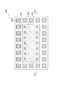
図6および図7は、本発明の第3の実施形態に係る半導体装置300の構成図であり、図6は半導体LSIチップ201の上面図、図7は半導体LSIチップ201を実装した場合における図6のA−A断面図である。図1と同一構成部分には同一符号を付して重複箇所の説明を省略する。
図6に示すように、半導体装置300は、半導体LSIチップ201上に、トランジスタ、ダイオード、抵抗素子等複数の半導体素子が形成され、それらを制御する入出力電極PAD202が配置されている。
半導体LSIチップ201は、半導体基板208上に、トランジスタ、ダイオード、抵抗素子等の複数の半導体素子(図示省略)が形成されている。各半導体素子の電極等の配線は、絶縁酸化膜110内に形成された多層配線203を介して電気的に入出力電極PAD202に接続される。半導体LSIチップ201の各半導体素子は、多層配線203および入出力電極PAD202を通して導電部材102に接続される。
図8および図9は、本発明の第4の実施形態に係る半導体装置400の構成図であり、図8は半導体LSIチップ205,206の上面図、図9は半導体LSIチップ205,206を実装した場合における図8のB−B断面図である。図6および図7と同一構成部分には同一符号を付して重複箇所の説明を省略する。
図8に示すように、半導体装置400は、第1の半導体LSIチップ205と第2の半導体LSIチップ206とを積層構造にした構成を採る。
図9に示すように、半導体装置300は、第1の半導体LSIチップ205と、第2の半導体LSIチップ206と、半導体LSIチップ205の複数電極と多層配線203を介して接続された複数の入出力電極PAD202と、第1の半導体LSIチップ205と第2の半導体LSIチップ206とを電気的に接続するチップ間接続電極PAD207と、を備える。
第1の半導体LSIチップ205と第2の半導体LSIチップ206を電気的に接続するチップ間接続電極PAD207が配置され、第1の半導体LSIチップ205および第2の半導体LSIチップ206の半導体LSIチップを制御する入出力電極PAD202が配置されている。
また、本実施形態では、複数の半導体チップを積層することが可能であり、パッケージの小型化が可能である。
本発明の半導体装置を電力変換装置に適用した第3の実施形態について説明する。
図10は、第1の実施形態に係る半導体装置100を採用した電力変換装置500を示す回路図である。図10は、本実施形態の電力変換装置500の回路構成の一例と直流電源と三相交流モータ(交流負荷)との接続の関係を示す。
本実施形態の電力変換装置500では、第1の実施形態の半導体装置100を電力スイッチング素子501〜506として用いている。電力スイッチング素子501〜506は、例えばIGBTである。
また、一対の電力スイッチング素子501および502の直列接続からなり、その直列接続点に接続されるU端子533を出力とするスイッチングレッグを備える。また、それと同じ構成の電力スイッチング素子503および504の直列接続からなり、その直列接続点に接続されるV端子534を出力とするスイッチングレッグを備える。また、それと同じ構成の電力スイッチング素子505および506の直列接続からなり、その直列接続点に接続されるW端子535を出力とするスイッチングレッグを備える。
電力スイッチング素子501〜506は、例えばIGBTである。
電力スイッチング素子501〜506には、それぞれ逆並列にダイオード521〜526が接続されている。IGBTからなる電力スイッチング素子501〜506のそれぞれのゲートの入力端子には、ゲート回路511〜516によって制御される。なお、ゲート回路511〜516は統括制御回路(不図示)によって統括的に制御されている。
ゲート回路511〜516によって、それぞれ電力スイッチング素子501〜506を統括的に適切に制御して、直流電源Vccの直流電力は、三相交流電力に変換され、U端子533、V端子534、W端子535から出力される。
本発明は、電子部品中の電気的接合部(例えば、半導体素子と回路部材との接合部)の接合層に関し、特に、酸化銅粒子を主材とする接合材を用いて接合した接合層を有する半導体装置に適用して好適である。
以上、各実施形態について図面を参照して詳述したが、本発明はこれら実施形態に限定されるものではなく、本発明の要旨を逸脱しない範囲の工程、製造、設計変更等があってもよく、以下にその例を挙げる。
例えば、半導体素子の第1導電型をn型とし、第2導電型をp型とする構成のほか、第1導電型をp型とし、第2導電型をn型としても同様に成り立つ。
91 アノードP型半導体層
92 カソードn+層
100,200,300,400 半導体装置
101 セラミック基板
102 導電部材
103 銅焼結層
104 Ni層(金属層)
104a Ni層の表面
105 第1のAl金属層
106 第2のAl金属層
106a 第2のAl金属層の表面
107 Cu拡散防止層
108 半導体基板
108a p型半導体層
108b n−ドリフト層
108c n+型半導体層
108d 半導体基板の第1表面
108e 半導体基板の第2表面
109アノード電極
110絶縁酸化膜
111 パッシベーション膜
112 カソード電極
113,119,403 絶縁膜
150 半導体素子
151 第1の半導体チップの電極構造体
152 第2の半導体チップの電極構造体
201 半導体LSIチップ
202 入出力電極PAD
203 多層配線
204 基板
205 第1の半導体LSIチップ
206 第2の半導体LSIチップ
207 チップ間接続電極PAD
500 電力変換装置
501〜506 電力スイッチング素子
521〜526 ダイオード
511〜516 ゲート回路
Claims (6)
- 半導体素子が形成された半導体基板の第1表面に、
前記半導体素子と電気的に接続され、AlもしくはAl合金からなる第1のAl金属層、Cu拡散防止層、AlもしくはAl合金からなる第2のAl金属層、および金属層がこの順に形成されている第1の半導体チップの電極構造体と、
前記第1の半導体チップの電極構造体における前記金属層の表面に配置され、銅焼結層を介して前記第1の半導体チップの電極構造体と接合された導電部材と、を備え、
前記第2のAl金属層は、
表面のAl結晶粒の結晶面方位が主に(110)面、かつ、平均結晶粒の大きさが、0.5μm以上となるように形成されている
ことを特徴とする半導体装置。 - 前記半導体基板の第2表面に、
AlもしくはAl合金からなる第1のAl金属層、Cu拡散防止層、AlもしくはAl合金からなる第2のAl金属層、および金属層がこの順に形成されている第2の半導体チップの電極構造体と、
第2の半導体チップの電極構造体における前記金属層の表面に配置され、銅焼結層を介して前記第2の半導体チップの電極構造体と接合された導電部材と、をさらに備え、
前記第2のAl金属層は、
表面のAl結晶粒の結晶面方位が主に(110)面、かつ、平均結晶粒の大きさが、0.5μm以上となるように形成されている
ことを特徴とする請求項1に記載の半導体装置。 - 半導体基板に形成された複数の素子と当該素子に電気的に接続する接続電極パッドを備え、
前記接続電極パッドは、
前記素子が形成された半導体基板の表面に、
前記素子と電気的に接続され、AlもしくはAl合金からなる第1のAl金属層、Cu拡散防止層、AlもしくはAl合金からなる第2のAl金属層、および金属層がこの順に形成されている第1の半導体チップの電極構造体と、
前記金属層の表面に配置され、銅焼結層を介して前記第1の半導体チップの電極構造体と接合された導電部材と、を備え、
前記第2のAl金属層は、
表面のAl結晶粒の結晶面方位が主に(110)面、かつ、平均結晶粒の大きさが、0.5μm以上となるように形成されている
ことを特徴とする半導体装置。 - 請求項1において、
前記半導体素子が形成された前記半導体基板を用意する工程と、
前記半導体基板の表面に前記第1のAl金属層を形成する工程と、
前記第1のAl金属層の表面に、前記第1のAl金属層の導電性を確保しつつ、前記銅焼結層のCu拡散を防止するCu拡散防止層を形成する工程と、
前記Cu拡散防止層の表面に、前記第1のAl金属層と同一材料からなる前記第2のAl金属層を形成する工程と、
前記第2のAl金属層上に前記金属層を形成する工程と、
前記半導体基板をチップ化することで、前記第1の半導体チップの電極構造体を形成する工程と、
前記銅焼結層を介して、前記第1の半導体チップの電極構造体を互いに接合する工程と、
を有し、
前記第2のAl金属層を形成する工程では、前記第2のAl金属層の平均結晶粒の大きさが、0.5μm以上となる条件でスパッタリングを用いて形成されていることを特徴とする半導体装置の製造方法。 - 前記スパッタリングは、低温スパッタリング条件、かつ、200℃以下の成膜条件である
ことを特徴とする請求項4に記載の半導体方法。 - 一対の直流端子と、交流の相数と同数の交流端子と、前記一対の直流端子間に接続された、それぞれのスイッチング素子と逆極性のダイオードの並列回路を2個直列に接続した構成からなり、前記並列回路の相互接続点が異なる交流端子に接続された交流の相数と同数の電力変換単位とを備え、前記スイッチング素子が請求項1乃至請求項3のいずれか一項に記載の半導体装置であることを特徴とする電力変換装置。
Priority Applications (4)
| Application Number | Priority Date | Filing Date | Title |
|---|---|---|---|
| JP2015036099A JP6300236B2 (ja) | 2015-02-26 | 2015-02-26 | 半導体装置、半導体装置の製造方法および電力変換装置 |
| US15/051,822 US20160254761A1 (en) | 2015-02-26 | 2016-02-24 | Semiconductor device, method of manufacturing semiconductor device, and power conversion device |
| CN201610104398.2A CN105931954A (zh) | 2015-02-26 | 2016-02-25 | 半导体装置、半导体装置的制造方法以及电力变换装置 |
| EP16157345.6A EP3062341A3 (en) | 2015-02-26 | 2016-02-25 | Semiconductor device with an electrode structure comprising an aluminium or aluminium alloy layer with {110} texture, method of manufacturing said semiconductor device and power conversion device comprising said semiconductor device |
Applications Claiming Priority (1)
| Application Number | Priority Date | Filing Date | Title |
|---|---|---|---|
| JP2015036099A JP6300236B2 (ja) | 2015-02-26 | 2015-02-26 | 半導体装置、半導体装置の製造方法および電力変換装置 |
Publications (2)
| Publication Number | Publication Date |
|---|---|
| JP2016157882A JP2016157882A (ja) | 2016-09-01 |
| JP6300236B2 true JP6300236B2 (ja) | 2018-03-28 |
Family
ID=55411321
Family Applications (1)
| Application Number | Title | Priority Date | Filing Date |
|---|---|---|---|
| JP2015036099A Active JP6300236B2 (ja) | 2015-02-26 | 2015-02-26 | 半導体装置、半導体装置の製造方法および電力変換装置 |
Country Status (4)
| Country | Link |
|---|---|
| US (1) | US20160254761A1 (ja) |
| EP (1) | EP3062341A3 (ja) |
| JP (1) | JP6300236B2 (ja) |
| CN (1) | CN105931954A (ja) |
Families Citing this family (14)
| Publication number | Priority date | Publication date | Assignee | Title |
|---|---|---|---|---|
| JP6436531B2 (ja) * | 2015-01-30 | 2018-12-12 | 住友電工デバイス・イノベーション株式会社 | 半導体装置の製造方法 |
| JP6455335B2 (ja) * | 2015-06-23 | 2019-01-23 | 三菱電機株式会社 | 半導体装置 |
| JP6816776B2 (ja) * | 2017-01-13 | 2021-01-20 | 三菱電機株式会社 | 半導体装置 |
| JP6726112B2 (ja) * | 2017-01-19 | 2020-07-22 | 株式会社 日立パワーデバイス | 半導体装置および電力変換装置 |
| JP2018121050A (ja) * | 2017-01-24 | 2018-08-02 | トヨタ自動車株式会社 | 半導体装置とその製造方法 |
| CN108346700B (zh) * | 2017-01-24 | 2021-10-12 | 株式会社电装 | 半导体装置及其制造方法 |
| JP6952552B2 (ja) * | 2017-09-27 | 2021-10-20 | 株式会社日立製作所 | 接続材料および熱電変換モジュールならびに電子装置 |
| US10741783B2 (en) * | 2018-01-25 | 2020-08-11 | Wuhan China Star Optoelectronics Semiconductor Display Technology Co., Ltd. | Light emitting device and manufacturing method for the same |
| JP7075847B2 (ja) * | 2018-08-28 | 2022-05-26 | 株式会社 日立パワーデバイス | 半導体装置および電力変換装置 |
| US20220003808A1 (en) * | 2019-03-01 | 2022-01-06 | Mitsubishi Electric Corporation | Semiconductor device and method for diagnosing deterioration of semiconductor device |
| JP7249927B2 (ja) * | 2019-11-07 | 2023-03-31 | 三菱電機株式会社 | 半導体装置およびその製造方法 |
| KR102196385B1 (ko) * | 2020-05-04 | 2020-12-30 | 제엠제코(주) | 반도체 패키지 |
| JP2023144467A (ja) * | 2022-03-28 | 2023-10-11 | 株式会社 日立パワーデバイス | 半導体装置および電力変換装置 |
| JP2023144454A (ja) * | 2022-03-28 | 2023-10-11 | 株式会社 日立パワーデバイス | 半導体装置、半導体装置および電力変換装置 |
Family Cites Families (11)
| Publication number | Priority date | Publication date | Assignee | Title |
|---|---|---|---|---|
| US4325239A (en) * | 1980-01-17 | 1982-04-20 | Supra Products, Inc. | Key safe having improved bar locking system |
| US4352239A (en) * | 1980-04-17 | 1982-10-05 | Fairchild Camera And Instrument | Process for suppressing electromigration in conducting lines formed on integrated circuits by control of crystalline boundary orientation |
| JP2001066620A (ja) * | 2000-07-10 | 2001-03-16 | Hitachi Ltd | 配線材料および液晶表示装置 |
| JP3767585B2 (ja) * | 2003-07-11 | 2006-04-19 | 株式会社デンソー | 半導体装置 |
| US7393771B2 (en) * | 2004-06-29 | 2008-07-01 | Hitachi, Ltd. | Method for mounting an electronic part on a substrate using a liquid containing metal particles |
| JP2007005368A (ja) * | 2005-06-21 | 2007-01-11 | Renesas Technology Corp | 半導体装置の製造方法 |
| JP4973046B2 (ja) * | 2006-07-20 | 2012-07-11 | 株式会社デンソー | 半導体装置の製造方法 |
| JP5006081B2 (ja) * | 2007-03-28 | 2012-08-22 | 株式会社日立製作所 | 半導体装置、その製造方法、複合金属体及びその製造方法 |
| JP2009111188A (ja) * | 2007-10-30 | 2009-05-21 | Denso Corp | 半導体装置 |
| JP5719740B2 (ja) * | 2011-09-30 | 2015-05-20 | 株式会社日立製作所 | 配線材料および、それを用いた半導体モジュール |
| JP2016004877A (ja) * | 2014-06-16 | 2016-01-12 | ルネサスエレクトロニクス株式会社 | 半導体装置および電子装置 |
-
2015
- 2015-02-26 JP JP2015036099A patent/JP6300236B2/ja active Active
-
2016
- 2016-02-24 US US15/051,822 patent/US20160254761A1/en not_active Abandoned
- 2016-02-25 CN CN201610104398.2A patent/CN105931954A/zh active Pending
- 2016-02-25 EP EP16157345.6A patent/EP3062341A3/en not_active Withdrawn
Also Published As
| Publication number | Publication date |
|---|---|
| EP3062341A2 (en) | 2016-08-31 |
| US20160254761A1 (en) | 2016-09-01 |
| JP2016157882A (ja) | 2016-09-01 |
| EP3062341A3 (en) | 2016-11-09 |
| CN105931954A (zh) | 2016-09-07 |
Similar Documents
| Publication | Publication Date | Title |
|---|---|---|
| JP6300236B2 (ja) | 半導体装置、半導体装置の製造方法および電力変換装置 | |
| JP6726112B2 (ja) | 半導体装置および電力変換装置 | |
| JP7075847B2 (ja) | 半導体装置および電力変換装置 | |
| US9997432B2 (en) | Semiconductor device and electronic component using the same | |
| JP6347309B2 (ja) | 半導体装置および半導体装置の製造方法 | |
| US11456359B2 (en) | Semiconductor device and method of manufacturing semiconductor device | |
| US10192811B2 (en) | Power semiconductor device | |
| US20170162482A1 (en) | Semiconductor device | |
| US11615963B2 (en) | Electronic device, electronic module and methods for fabricating the same | |
| JP2014120638A (ja) | パワーモジュール半導体装置およびその製造方法 | |
| JP2004363518A (ja) | 半導体装置の製造方法 | |
| JP2014032985A (ja) | 半導体装置およびその製造方法 | |
| TW201633539A (zh) | 半導體裝置及半導體封裝體 | |
| JP2018107481A (ja) | パワーモジュール半導体装置 | |
| JP2018206871A (ja) | 半導体素子及びその製造方法 | |
| CN108417567B (zh) | 半导体模块 | |
| EP3242322B1 (fr) | Dispositif electronique de puissance a structure d'interconnexion electrique plane | |
| JP2013009014A (ja) | 半導体装置 | |
| US20230307348A1 (en) | Semiconductor apparatus | |
| CN115050656A (zh) | 一种集成续流二极管的氮化镓功率器件以及封装方法 | |
| JP5151837B2 (ja) | 半導体装置の製造方法 | |
| JP2018200978A (ja) | 半導体装置 | |
| JPH0831999A (ja) | ダイオ−ドの放熱装置および該装置の実装方法 |
Legal Events
| Date | Code | Title | Description |
|---|---|---|---|
| A621 | Written request for application examination |
Free format text: JAPANESE INTERMEDIATE CODE: A621 Effective date: 20170317 |
|
| A977 | Report on retrieval |
Free format text: JAPANESE INTERMEDIATE CODE: A971007 Effective date: 20171019 |
|
| A131 | Notification of reasons for refusal |
Free format text: JAPANESE INTERMEDIATE CODE: A131 Effective date: 20171024 |
|
| A521 | Request for written amendment filed |
Free format text: JAPANESE INTERMEDIATE CODE: A523 Effective date: 20171221 |
|
| TRDD | Decision of grant or rejection written | ||
| A01 | Written decision to grant a patent or to grant a registration (utility model) |
Free format text: JAPANESE INTERMEDIATE CODE: A01 Effective date: 20180213 |
|
| A61 | First payment of annual fees (during grant procedure) |
Free format text: JAPANESE INTERMEDIATE CODE: A61 Effective date: 20180220 |
|
| R150 | Certificate of patent or registration of utility model |
Ref document number: 6300236 Country of ref document: JP Free format text: JAPANESE INTERMEDIATE CODE: R150 |
|
| S111 | Request for change of ownership or part of ownership |
Free format text: JAPANESE INTERMEDIATE CODE: R313117 |
|
| R350 | Written notification of registration of transfer |
Free format text: JAPANESE INTERMEDIATE CODE: R350 |