JP6282394B2 - パワーモジュール用基板 - Google Patents
パワーモジュール用基板 Download PDFInfo
- Publication number
- JP6282394B2 JP6282394B2 JP2012238636A JP2012238636A JP6282394B2 JP 6282394 B2 JP6282394 B2 JP 6282394B2 JP 2012238636 A JP2012238636 A JP 2012238636A JP 2012238636 A JP2012238636 A JP 2012238636A JP 6282394 B2 JP6282394 B2 JP 6282394B2
- Authority
- JP
- Japan
- Prior art keywords
- ceramic substrate
- copper plate
- substrate
- peripheral edge
- power module
- Prior art date
- Legal status (The legal status is an assumption and is not a legal conclusion. Google has not performed a legal analysis and makes no representation as to the accuracy of the status listed.)
- Active
Links
Images

Classifications
-
- H—ELECTRICITY
- H01—ELECTRIC ELEMENTS
- H01L—SEMICONDUCTOR DEVICES NOT COVERED BY CLASS H10
- H01L2224/00—Indexing scheme for arrangements for connecting or disconnecting semiconductor or solid-state bodies and methods related thereto as covered by H01L24/00
- H01L2224/01—Means for bonding being attached to, or being formed on, the surface to be connected, e.g. chip-to-package, die-attach, "first-level" interconnects; Manufacturing methods related thereto
- H01L2224/42—Wire connectors; Manufacturing methods related thereto
- H01L2224/47—Structure, shape, material or disposition of the wire connectors after the connecting process
- H01L2224/48—Structure, shape, material or disposition of the wire connectors after the connecting process of an individual wire connector
- H01L2224/4805—Shape
- H01L2224/4809—Loop shape
- H01L2224/48091—Arched
Landscapes
- Cooling Or The Like Of Semiconductors Or Solid State Devices (AREA)
Description
従来のパワーモジュール用基板や、特開平2−72696号公報、特開平7−321447号公報で開示されようなパワーモジュール用基板は、表銅板の少なくとも1つにセラミック基板の縁部に重なって、あるいは、セラミック基板の縁部から外れて外部に延設して接合される場合に、セラミック基板の縁部の部分的な突出や、バリ状の突起によって表銅板がセラミック基板から浮き上がった状態となりセラミック基板との当接部に空隙部であるボイドが発生したり、不着面積が多くなって、セラミック基板と銅板との間の熱伝導性が低下すると共に、銅板のセラミック基板との接着強度が低くなり、接合信頼性の低下となっている。
本発明は、かかる事情に鑑みてなされたものであって、銅板とセラミック基板間の熱伝導性に優れ、銅板とセラミック基板の接着強度が高く接合信頼性の高いパワーモジュール用基板を提供することを目的とする。
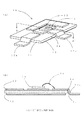
図1(A)、(B)に示すように、本発明の一実施の形態に係るパワーモジュール用基板10は、焼成済の所定寸法からなる平板状のセラミック基板11の一方の主面である上面側にそれぞれパターンが形成された表銅板12と、セラミック基板11の他方の主面である下面側にベタ状態のパターンからなる裏銅板13を有している。この表銅板12や、裏銅板13は、アルミナ(Al2O3)、ジルコニア系アルミナ、窒化アルミニウム(AlN)等のセラミックからなる焼成済のセラミック基板11に直接接合、又は活性金属ろう材接合で加熱接合されるようになっている。
図2(A)、(B)に示すように、パワーモジュール用基板10aは、焼成済の所定寸法からなる平板のセラミック基板11aの所定位置には、所定寸法からなる貫通孔17が設けられている。そして、パワーモジュール用基板10aには、セラミック基板11aの一方の主面である上面側にそれぞれパターンが形成された表銅板12が貫通孔17の開口を露出するようにして設けられている。また、パワーモジュール用基板10aには、セラミック基板11aの他方の主面である下面側にベタ状態のパターンからなる裏銅板13が貫通孔17の開口を塞ぐようにして設けられている。このパワーモジュール用基板10aは、表銅板12や、裏銅板13がアルミナ(Al2O3)、ジルコニア系アルミナ、窒化アルミニウム(AlN)等のセラミックからなる焼成済のセラミック基板11aに直接接合、又は活性金属ろう材接合で加熱接合されるようになっている。なお、この直接接合での接合方法や、活性金属ろう材接合での接合方法とは、前記のパワーモジュール用基板10の場合と同様な接合方法である。
Claims (2)
- セラミック基板の一方の主面にそれぞれパターンが形成された複数の表銅板、他方の主面にベタ状の裏銅板が直接接合法で接合されて有するパワーモジュール用基板において、
少なくとも1つの前記表銅板の一方側が前記セラミック基板に接合され、他方側が前記セラミック基板の外周縁部から中空状態で外部に延設され、前記表銅板の前記他方側は、前記セラミック基板の前記外周縁部に形成された面取り状の曲部に当接されていることを特徴とするパワーモジュール用基板。 - セラミック基板の一方の主面にそれぞれパターンが形成された複数の表銅板、他方の主面にベタ状の裏銅板が直接接合法で接合されて有するパワーモジュール用基板において、
前記セラミック基板の外周縁部及び前記セラミック基板に設けられる貫通孔の外周である内周縁部には面取り状の曲部が形成され、
少なくとも1つの前記表銅板の一方側が前記セラミック基板の前記内周縁部に重なって接合されると共に、他方側が前記セラミック基板の前記外周縁部から中空状態で外部に延設され、前記表銅板の前記他方側は、前記セラミック基板の前記外周縁部に形成された前記面取り状の曲部に当接されることを特徴とするパワーモジュール用基板。
Priority Applications (1)
| Application Number | Priority Date | Filing Date | Title |
|---|---|---|---|
| JP2012238636A JP6282394B2 (ja) | 2012-10-30 | 2012-10-30 | パワーモジュール用基板 |
Applications Claiming Priority (1)
| Application Number | Priority Date | Filing Date | Title |
|---|---|---|---|
| JP2012238636A JP6282394B2 (ja) | 2012-10-30 | 2012-10-30 | パワーモジュール用基板 |
Publications (2)
| Publication Number | Publication Date |
|---|---|
| JP2014090048A JP2014090048A (ja) | 2014-05-15 |
| JP6282394B2 true JP6282394B2 (ja) | 2018-02-21 |
Family
ID=50791734
Family Applications (1)
| Application Number | Title | Priority Date | Filing Date |
|---|---|---|---|
| JP2012238636A Active JP6282394B2 (ja) | 2012-10-30 | 2012-10-30 | パワーモジュール用基板 |
Country Status (1)
| Country | Link |
|---|---|
| JP (1) | JP6282394B2 (ja) |
Family Cites Families (10)
| Publication number | Priority date | Publication date | Assignee | Title |
|---|---|---|---|---|
| JPS58219751A (ja) * | 1982-06-15 | 1983-12-21 | Yokogawa Hokushin Electric Corp | 混成集積回路の製造方法 |
| JPH06151637A (ja) * | 1992-11-13 | 1994-05-31 | Denki Kagaku Kogyo Kk | リード付き窒化アルミニウム絶縁放熱板 |
| US5455386A (en) * | 1994-01-14 | 1995-10-03 | Olin Corporation | Chamfered electronic package component |
| JPH07321447A (ja) * | 1994-05-20 | 1995-12-08 | Toyota Autom Loom Works Ltd | 電子部品搭載用基板及びその製造方法、並びに電子部品搭載用基板製造用の金属板材及び接合防止マスク |
| JP4726021B2 (ja) * | 1998-08-11 | 2011-07-20 | 株式会社村田製作所 | セラミック生ユニットのバリ取り装置 |
| JP2001156196A (ja) * | 1999-09-17 | 2001-06-08 | Toshiba Corp | 高周波パッケージおよびその製造方法 |
| JP3712378B2 (ja) * | 2002-01-25 | 2005-11-02 | 電気化学工業株式会社 | 端子付き回路基板及びその製造方法 |
| JP3850335B2 (ja) * | 2002-02-25 | 2006-11-29 | 京セラ株式会社 | セラミック回路基板 |
| JP3984107B2 (ja) * | 2002-06-07 | 2007-10-03 | 株式会社住友金属エレクトロデバイス | 高周波用半導体素子収納用パッケージの製造方法 |
| JP2004095690A (ja) * | 2002-08-29 | 2004-03-25 | Kyocera Corp | セラミック基板の製造方法 |
-
2012
- 2012-10-30 JP JP2012238636A patent/JP6282394B2/ja active Active
Also Published As
| Publication number | Publication date |
|---|---|
| JP2014090048A (ja) | 2014-05-15 |
Similar Documents
| Publication | Publication Date | Title |
|---|---|---|
| US12033915B2 (en) | Power module substrate and power module | |
| JP4981696B2 (ja) | パッケージ | |
| JP6140834B2 (ja) | 配線基板および電子装置 | |
| JP2008010520A (ja) | パワーモジュール用基板及びその製造方法 | |
| JP4124040B2 (ja) | 半導体装置 | |
| JP2007019123A (ja) | セラミック回路基板集合体 | |
| JP2014157949A (ja) | 配線基板および電子装置 | |
| JP6282394B2 (ja) | パワーモジュール用基板 | |
| WO2019163941A1 (ja) | パワーモジュール用基板およびパワーモジュール | |
| JP3993619B2 (ja) | セラミック回路基板集合体 | |
| JP6124521B2 (ja) | パワーモジュール用基板の製造方法 | |
| JP6108734B2 (ja) | 電子部品素子収納用パッケージ | |
| JP2014090049A (ja) | パワーモジュール用基板 | |
| JP2014154571A (ja) | パワーモジュール用基板 | |
| JP3971554B2 (ja) | セラミック回路基板およびこれを用いた半導体モジュール | |
| JP2004087927A (ja) | セラミック回路基板 | |
| JP4656126B2 (ja) | 半導体装置 | |
| JP6235272B2 (ja) | 半導体素子搭載用基板およびそれを備えた半導体装置 | |
| JP2009277794A (ja) | 半導体素子収納用パッケージ | |
| JP2008124298A (ja) | パワーモジュール用基板の製造方法 | |
| JP4721929B2 (ja) | 多層回路基板および電子部品モジュール | |
| JP2009158530A (ja) | パワーモジュール用基板の製造方法 | |
| JP2003198077A (ja) | セラミック回路基板 | |
| JP2014011435A (ja) | セラミック複合基板 | |
| JP2000277872A (ja) | 配線基板 |
Legal Events
| Date | Code | Title | Description |
|---|---|---|---|
| A621 | Written request for application examination |
Free format text: JAPANESE INTERMEDIATE CODE: A621 Effective date: 20151015 |
|
| A977 | Report on retrieval |
Free format text: JAPANESE INTERMEDIATE CODE: A971007 Effective date: 20160825 |
|
| A131 | Notification of reasons for refusal |
Free format text: JAPANESE INTERMEDIATE CODE: A131 Effective date: 20160912 |
|
| A521 | Request for written amendment filed |
Free format text: JAPANESE INTERMEDIATE CODE: A523 Effective date: 20161111 |
|
| RD02 | Notification of acceptance of power of attorney |
Free format text: JAPANESE INTERMEDIATE CODE: A7422 Effective date: 20161111 |
|
| A131 | Notification of reasons for refusal |
Free format text: JAPANESE INTERMEDIATE CODE: A131 Effective date: 20170217 |
|
| A521 | Request for written amendment filed |
Free format text: JAPANESE INTERMEDIATE CODE: A523 Effective date: 20170417 |
|
| A131 | Notification of reasons for refusal |
Free format text: JAPANESE INTERMEDIATE CODE: A131 Effective date: 20171003 |
|
| A521 | Request for written amendment filed |
Free format text: JAPANESE INTERMEDIATE CODE: A523 Effective date: 20171031 |
|
| TRDD | Decision of grant or rejection written | ||
| A01 | Written decision to grant a patent or to grant a registration (utility model) |
Free format text: JAPANESE INTERMEDIATE CODE: A01 Effective date: 20180119 |
|
| A61 | First payment of annual fees (during grant procedure) |
Free format text: JAPANESE INTERMEDIATE CODE: A61 Effective date: 20180124 |
|
| R150 | Certificate of patent or registration of utility model |
Ref document number: 6282394 Country of ref document: JP Free format text: JAPANESE INTERMEDIATE CODE: R150 |
|
| R250 | Receipt of annual fees |
Free format text: JAPANESE INTERMEDIATE CODE: R250 |
|
| R250 | Receipt of annual fees |
Free format text: JAPANESE INTERMEDIATE CODE: R250 |
|
| R250 | Receipt of annual fees |
Free format text: JAPANESE INTERMEDIATE CODE: R250 |
|
| R250 | Receipt of annual fees |
Free format text: JAPANESE INTERMEDIATE CODE: R250 |
|
| R250 | Receipt of annual fees |
Free format text: JAPANESE INTERMEDIATE CODE: R250 |