JP6257713B2 - Method for manufacturing semiconductor device - Google Patents
Method for manufacturing semiconductor device Download PDFInfo
- Publication number
- JP6257713B2 JP6257713B2 JP2016156184A JP2016156184A JP6257713B2 JP 6257713 B2 JP6257713 B2 JP 6257713B2 JP 2016156184 A JP2016156184 A JP 2016156184A JP 2016156184 A JP2016156184 A JP 2016156184A JP 6257713 B2 JP6257713 B2 JP 6257713B2
- Authority
- JP
- Japan
- Prior art keywords
- layer
- transistor
- insulating layer
- semiconductor
- conductive layer
- Prior art date
- Legal status (The legal status is an assumption and is not a legal conclusion. Google has not performed a legal analysis and makes no representation as to the accuracy of the status listed.)
- Expired - Fee Related
Links
Images


Classifications
-
- H—ELECTRICITY
- H10—SEMICONDUCTOR DEVICES; ELECTRIC SOLID-STATE DEVICES NOT OTHERWISE PROVIDED FOR
- H10B—ELECTRONIC MEMORY DEVICES
- H10B99/00—Subject matter not provided for in other groups of this subclass
-
- G—PHYSICS
- G11—INFORMATION STORAGE
- G11C—STATIC STORES
- G11C11/00—Digital stores characterised by the use of particular electric or magnetic storage elements; Storage elements therefor
- G11C11/21—Digital stores characterised by the use of particular electric or magnetic storage elements; Storage elements therefor using electric elements
- G11C11/34—Digital stores characterised by the use of particular electric or magnetic storage elements; Storage elements therefor using electric elements using semiconductor devices
- G11C11/40—Digital stores characterised by the use of particular electric or magnetic storage elements; Storage elements therefor using electric elements using semiconductor devices using transistors
- G11C11/401—Digital stores characterised by the use of particular electric or magnetic storage elements; Storage elements therefor using electric elements using semiconductor devices using transistors forming cells needing refreshing or charge regeneration, i.e. dynamic cells
- G11C11/403—Digital stores characterised by the use of particular electric or magnetic storage elements; Storage elements therefor using electric elements using semiconductor devices using transistors forming cells needing refreshing or charge regeneration, i.e. dynamic cells with charge regeneration common to a multiplicity of memory cells, i.e. external refresh
- G11C11/405—Digital stores characterised by the use of particular electric or magnetic storage elements; Storage elements therefor using electric elements using semiconductor devices using transistors forming cells needing refreshing or charge regeneration, i.e. dynamic cells with charge regeneration common to a multiplicity of memory cells, i.e. external refresh with three charge-transfer gates, e.g. MOS transistors, per cell
-
- H—ELECTRICITY
- H01—ELECTRIC ELEMENTS
- H01L—SEMICONDUCTOR DEVICES NOT COVERED BY CLASS H10
- H01L21/00—Processes or apparatus adapted for the manufacture or treatment of semiconductor or solid state devices or of parts thereof
- H01L21/70—Manufacture or treatment of devices consisting of a plurality of solid state components formed in or on a common substrate or of parts thereof; Manufacture of integrated circuit devices or of parts thereof
- H01L21/77—Manufacture or treatment of devices consisting of a plurality of solid state components or integrated circuits formed in, or on, a common substrate
- H01L21/78—Manufacture or treatment of devices consisting of a plurality of solid state components or integrated circuits formed in, or on, a common substrate with subsequent division of the substrate into plural individual devices
- H01L21/82—Manufacture or treatment of devices consisting of a plurality of solid state components or integrated circuits formed in, or on, a common substrate with subsequent division of the substrate into plural individual devices to produce devices, e.g. integrated circuits, each consisting of a plurality of components
- H01L21/84—Manufacture or treatment of devices consisting of a plurality of solid state components or integrated circuits formed in, or on, a common substrate with subsequent division of the substrate into plural individual devices to produce devices, e.g. integrated circuits, each consisting of a plurality of components the substrate being other than a semiconductor body, e.g. being an insulating body
-
- H—ELECTRICITY
- H01—ELECTRIC ELEMENTS
- H01L—SEMICONDUCTOR DEVICES NOT COVERED BY CLASS H10
- H01L27/00—Devices consisting of a plurality of semiconductor or other solid-state components formed in or on a common substrate
- H01L27/02—Devices consisting of a plurality of semiconductor or other solid-state components formed in or on a common substrate including semiconductor components specially adapted for rectifying, oscillating, amplifying or switching and having at least one potential-jump barrier or surface barrier; including integrated passive circuit elements with at least one potential-jump barrier or surface barrier
- H01L27/12—Devices consisting of a plurality of semiconductor or other solid-state components formed in or on a common substrate including semiconductor components specially adapted for rectifying, oscillating, amplifying or switching and having at least one potential-jump barrier or surface barrier; including integrated passive circuit elements with at least one potential-jump barrier or surface barrier the substrate being other than a semiconductor body, e.g. an insulating body
- H01L27/1203—Devices consisting of a plurality of semiconductor or other solid-state components formed in or on a common substrate including semiconductor components specially adapted for rectifying, oscillating, amplifying or switching and having at least one potential-jump barrier or surface barrier; including integrated passive circuit elements with at least one potential-jump barrier or surface barrier the substrate being other than a semiconductor body, e.g. an insulating body the substrate comprising an insulating body on a semiconductor body, e.g. SOI
-
- H—ELECTRICITY
- H01—ELECTRIC ELEMENTS
- H01L—SEMICONDUCTOR DEVICES NOT COVERED BY CLASS H10
- H01L27/00—Devices consisting of a plurality of semiconductor or other solid-state components formed in or on a common substrate
- H01L27/02—Devices consisting of a plurality of semiconductor or other solid-state components formed in or on a common substrate including semiconductor components specially adapted for rectifying, oscillating, amplifying or switching and having at least one potential-jump barrier or surface barrier; including integrated passive circuit elements with at least one potential-jump barrier or surface barrier
- H01L27/12—Devices consisting of a plurality of semiconductor or other solid-state components formed in or on a common substrate including semiconductor components specially adapted for rectifying, oscillating, amplifying or switching and having at least one potential-jump barrier or surface barrier; including integrated passive circuit elements with at least one potential-jump barrier or surface barrier the substrate being other than a semiconductor body, e.g. an insulating body
- H01L27/1214—Devices consisting of a plurality of semiconductor or other solid-state components formed in or on a common substrate including semiconductor components specially adapted for rectifying, oscillating, amplifying or switching and having at least one potential-jump barrier or surface barrier; including integrated passive circuit elements with at least one potential-jump barrier or surface barrier the substrate being other than a semiconductor body, e.g. an insulating body comprising a plurality of TFTs formed on a non-semiconducting substrate, e.g. driving circuits for AMLCDs
- H01L27/1222—Devices consisting of a plurality of semiconductor or other solid-state components formed in or on a common substrate including semiconductor components specially adapted for rectifying, oscillating, amplifying or switching and having at least one potential-jump barrier or surface barrier; including integrated passive circuit elements with at least one potential-jump barrier or surface barrier the substrate being other than a semiconductor body, e.g. an insulating body comprising a plurality of TFTs formed on a non-semiconducting substrate, e.g. driving circuits for AMLCDs with a particular composition, shape or crystalline structure of the active layer
- H01L27/1225—Devices consisting of a plurality of semiconductor or other solid-state components formed in or on a common substrate including semiconductor components specially adapted for rectifying, oscillating, amplifying or switching and having at least one potential-jump barrier or surface barrier; including integrated passive circuit elements with at least one potential-jump barrier or surface barrier the substrate being other than a semiconductor body, e.g. an insulating body comprising a plurality of TFTs formed on a non-semiconducting substrate, e.g. driving circuits for AMLCDs with a particular composition, shape or crystalline structure of the active layer with semiconductor materials not belonging to the group IV of the periodic table, e.g. InGaZnO
-
- H—ELECTRICITY
- H01—ELECTRIC ELEMENTS
- H01L—SEMICONDUCTOR DEVICES NOT COVERED BY CLASS H10
- H01L28/00—Passive two-terminal components without a potential-jump or surface barrier for integrated circuits; Details thereof; Multistep manufacturing processes therefor
- H01L28/40—Capacitors
-
- H—ELECTRICITY
- H10—SEMICONDUCTOR DEVICES; ELECTRIC SOLID-STATE DEVICES NOT OTHERWISE PROVIDED FOR
- H10B—ELECTRONIC MEMORY DEVICES
- H10B12/00—Dynamic random access memory [DRAM] devices
-
- H—ELECTRICITY
- H10—SEMICONDUCTOR DEVICES; ELECTRIC SOLID-STATE DEVICES NOT OTHERWISE PROVIDED FOR
- H10B—ELECTRONIC MEMORY DEVICES
- H10B41/00—Electrically erasable-and-programmable ROM [EEPROM] devices comprising floating gates
- H10B41/70—Electrically erasable-and-programmable ROM [EEPROM] devices comprising floating gates the floating gate being an electrode shared by two or more components
-
- G—PHYSICS
- G11—INFORMATION STORAGE
- G11C—STATIC STORES
- G11C16/00—Erasable programmable read-only memories
- G11C16/02—Erasable programmable read-only memories electrically programmable
- G11C16/04—Erasable programmable read-only memories electrically programmable using variable threshold transistors, e.g. FAMOS
- G11C16/0408—Erasable programmable read-only memories electrically programmable using variable threshold transistors, e.g. FAMOS comprising cells containing floating gate transistors
- G11C16/0433—Erasable programmable read-only memories electrically programmable using variable threshold transistors, e.g. FAMOS comprising cells containing floating gate transistors comprising cells containing a single floating gate transistor and one or more separate select transistors
Description
本発明の一態様は、半導体装置及び半導体記憶装置に関する。 One embodiment of the present invention relates to a semiconductor device and a semiconductor memory device.
近年、データの書き込み及び消去が可能であり、電源の供給がなくても一定期間データの
保持が可能な記憶回路を具備する半導体装置の開発が進められている。
In recent years, development of semiconductor devices including a memory circuit which can write and erase data and can hold data for a certain period without supply of power has been advanced.
上記半導体装置としては、例えば記憶素子であるトランジスタ(メモリトランジスタとも
いう)を備える記憶回路を具備する半導体装置が挙げられる(例えば特許文献1)。
As the semiconductor device, for example, a semiconductor device including a memory circuit including a transistor (also referred to as a memory transistor) which is a memory element can be given (for example, Patent Document 1).
特許文献1に示す半導体装置において、メモリトランジスタは、制御ゲート電極と、チャ
ネル形成層と、制御ゲート電極及びチャネル形成層の間に設けられた浮遊ゲート電極と、
を含む。上記浮遊ゲート電極にデータとなる電荷が蓄積されることにより、メモリトラン
ジスタにデータが書き込まれる。
In the semiconductor device described in
including. Data is written in the memory transistor by accumulating charges as data in the floating gate electrode.
しかしながら、特許文献1に示すような従来の半導体装置は、メモリトランジスタにデー
タが書き込まれた後に、電荷のリークによりデータが消失してしまうといった問題があっ
た。データの記憶が可能な半導体装置において、データの保持期間は、より長いことが望
ましい。
However, the conventional semiconductor device as shown in
また、従来の半導体装置は、動作させるために必要な電圧が高いため、消費電力が大きく
、また、印加される電圧により記憶素子が劣化してしまうといった問題があった。
In addition, the conventional semiconductor device has a problem that power consumption is large because a voltage required for operation is high, and a storage element is deteriorated by an applied voltage.
また、従来の半導体装置では、データの書き込みの際に、メモリトランジスタにおいてト
ンネル電流が生じ、記憶素子が劣化するため、繰り返しデータを書き込むと、記憶素子に
データが書き込めなくなるといった問題があった。
Further, in the conventional semiconductor device, when data is written, a tunnel current is generated in the memory transistor and the storage element is deteriorated. Therefore, when data is repeatedly written, the data cannot be written to the storage element.
本発明の一態様では、半導体装置又は半導体記憶装置におけるデータの保持期間を長くす
ることを課題の一つとする。また、本発明の一態様では、消費電力を低減することを課題
の一つとする。また、本発明の一態様では、記憶素子へのデータの書き込み可能回数を増
やすことを課題の一つとする。
An object of one embodiment of the present invention is to lengthen a data retention period in a semiconductor device or a semiconductor memory device. Another object of one embodiment of the present invention is to reduce power consumption. Another object of one embodiment of the present invention is to increase the number of times data can be written to a memory element.
本発明の一態様は、選択トランジスタ及び出力トランジスタを備える記憶回路を有し、該
選択トランジスタは、第1のゲート及び第2のゲートを有するものである。第1のゲート
及び第2のゲートの電圧により選択トランジスタの閾値電圧を必要に応じて調整し、選択
トランジスタがオフ状態のときに選択トランジスタのソース及びドレインの間に流れる電
流を極力少なくし、記憶回路におけるデータの保持時間を長くすることを図る。
One embodiment of the present invention includes a memory circuit including a selection transistor and an output transistor, and the selection transistor includes a first gate and a second gate. The threshold voltage of the selection transistor is adjusted as necessary by the voltage of the first gate and the second gate, and the current flowing between the source and the drain of the selection transistor when the selection transistor is in an off state is reduced as much as possible. The data retention time in the circuit is increased.
さらに、本発明の一態様において、上記出力トランジスタのチャネル形成層と上記選択ト
ランジスタのゲートとしての機能を有する層は、同じ材料である。これにより、同一工程
により上記出力トランジスタのチャネル形成層と上記選択トランジスタのゲートとしての
機能を有する層とを形成することを可能にし、製造工程数の増加の抑制を図る。
Further, in one embodiment of the present invention, the channel formation layer of the output transistor and the layer having a function as a gate of the selection transistor are formed using the same material. Accordingly, it is possible to form a channel formation layer of the output transistor and a layer having a function as a gate of the selection transistor by the same process, thereby suppressing an increase in the number of manufacturing steps.
本発明の一態様は、I行(Iは2以上の自然数)J列(Jは自然数)に配列され、第1の
ゲート及び第2のゲートを有する第1のトランジスタ、並びに第2のトランジスタをそれ
ぞれが備える複数のメモリセルを具備し、メモリセルは、それぞれ導電型を付与する不純
物元素を含有する一対の不純物領域を有し、第2のトランジスタのチャネル形成層として
の機能を有する第1の層と、第1の層と同時に形成され且つ同じ材料であり、第1の層と
離間し、不純物元素を含有し、第1のトランジスタの第2のゲートとしての機能を有する
第2の層と、第1の層及び第2の層の上に設けられ、第2のトランジスタのゲート絶縁層
としての機能を有する第1の絶縁層と、第1の絶縁層を介して第1の層に重畳し、第2の
トランジスタのゲートとしての機能を有する第1の導電層と、第1の絶縁層を介して第2
の層に重畳し、第1の層と異なる材料であり、第1のトランジスタのチャネル形成層とし
ての機能を有する半導体層と、半導体層に電気的に接続され、第1のトランジスタのソー
ス及びドレインの一方としての機能を有する第2の導電層と、第1の導電層及び半導体層
に電気的に接続され、第1のトランジスタのソース及びドレインの他方としての機能を有
する第3の導電層と、半導体層、第2の導電層、及び第3の導電層の上に設けられ、第1
のトランジスタのゲート絶縁層としての機能を有する第2の絶縁層と、第2の絶縁層を介
して半導体層に重畳し、第1のトランジスタの第1のゲートとしての機能を有する第4の
導電層と、第2の絶縁層及び第4の導電層の上に設けられた第3の絶縁層と、第1の絶縁
層乃至第3の絶縁層を貫通して設けられた第1の開口部を介して第1の層における一対の
不純物領域の一方に電気的に接続され、第2の絶縁層及び第3の絶縁層を貫通して設けら
れた第2の開口部を介して第3の導電層に電気的に接続された第5の導電層と、を含む半
導体記憶装置である。
According to one embodiment of the present invention, a first transistor having a first gate and a second gate, and a second transistor arranged in I rows (I is a natural number of 2 or more) J columns (J is a natural number) Each of the memory cells includes a plurality of memory cells. Each of the memory cells includes a pair of impurity regions each containing an impurity element imparting a conductivity type, and functions as a channel formation layer of the second transistor. A second layer formed simultaneously with the first layer and made of the same material, spaced apart from the first layer, containing an impurity element, and functioning as a second gate of the first transistor; A first insulating layer which is provided over the first layer and the second layer and functions as a gate insulating layer of the second transistor, and overlaps with the first layer through the first insulating layer And as the gate of the second transistor The second through the first conductive layer having a function, the first insulating layer
And a semiconductor layer which is a material different from that of the first layer and functions as a channel formation layer of the first transistor, and a source and a drain of the first transistor which are electrically connected to the semiconductor layer. A second conductive layer that functions as one of the first conductive layer, a third conductive layer that is electrically connected to the first conductive layer and the semiconductor layer, and functions as the other of the source and the drain of the first transistor; , Provided on the semiconductor layer, the second conductive layer, and the third conductive layer,
A second insulating layer that functions as a gate insulating layer of the first transistor, and a fourth conductive layer that overlaps with the semiconductor layer through the second insulating layer and functions as the first gate of the first transistor. Layer, a third insulating layer provided on the second insulating layer and the fourth conductive layer, and a first opening provided through the first to third insulating layers The third layer is electrically connected to one of the pair of impurity regions in the first layer through the second opening provided through the second insulating layer and the third insulating layer. And a fifth conductive layer electrically connected to the conductive layer.
本発明の一態様は、I行(Iは2以上の自然数)J列(Jは自然数)に配列され、第1の
ゲート及び第2のゲートを有する第1のトランジスタ、並びに第2のトランジスタをそれ
ぞれが備える複数のメモリセルを具備し、メモリセルは、導電型を付与する不純物元素を
含有する一対の不純物領域を有し、第2のトランジスタのチャネル形成層としての機能を
有する第1の層と、第1の層と同時に形成され且つ同じ材料であり、第1の層と離間し、
不純物元素を含有し、第1のトランジスタの第2のゲートとしての機能を有する第2の層
と、第1の層及び第2の層の上に設けられ、第2のトランジスタのゲート絶縁層としての
機能を有する第1の絶縁層と、第1の絶縁層を介して第1の層に重畳し、第2のトランジ
スタのゲートとしての機能を有する第1の導電層と、第1の絶縁層を介して第2の層に重
畳し、第1の層と異なる材料であり、第1のトランジスタのチャネル形成層としての機能
を有する半導体層と、半導体層に電気的に接続され、第1のトランジスタのソース及びド
レインの一方としての機能を有する第2の導電層と、第1の導電層及び半導体層に電気的
に接続され、第1のトランジスタのソース及びドレインの他方としての機能を有する第3
の導電層と、半導体層、第2の導電層、及び第3の導電層の上に設けられ、第1のトラン
ジスタのゲート絶縁層としての機能を有する第2の絶縁層と、第2の絶縁層を介して半導
体層に重畳し、第1のトランジスタの第1のゲートとしての機能を有する第4の導電層と
、を含み、同じ列に配置されるメモリセルにおいて、第1の層が同じ層の半導体記憶装置
である。
According to one embodiment of the present invention, a first transistor having a first gate and a second gate, and a second transistor arranged in I rows (I is a natural number of 2 or more) J columns (J is a natural number) Each of the memory cells includes a plurality of memory cells, each of which includes a pair of impurity regions containing an impurity element imparting a conductivity type and a first layer having a function as a channel formation layer of the second transistor And formed simultaneously with the first layer and of the same material, spaced apart from the first layer,
A second layer containing an impurity element and functioning as a second gate of the first transistor; and a gate insulating layer of the second transistor provided over the first layer and the second layer. A first insulating layer having the above function, a first conductive layer which overlaps with the first layer through the first insulating layer and functions as a gate of the second transistor, and the first insulating layer And a semiconductor layer which is different from the first layer and has a function as a channel formation layer of the first transistor, and is electrically connected to the semiconductor layer. A second conductive layer that functions as one of a source and a drain of the transistor, and a second conductive layer that is electrically connected to the first conductive layer and the semiconductor layer and functions as the other of the source and the drain of the first transistor 3
And a second insulating layer provided on the semiconductor layer, the second conductive layer, and the third conductive layer and functioning as a gate insulating layer of the first transistor, and a second insulating layer And the fourth conductive layer which functions as the first gate of the first transistor and overlaps with the semiconductor layer through the layer, and in the memory cells arranged in the same column, the first layer is the same A semiconductor memory device of a layer.
本発明の一態様により、半導体装置又は半導体記憶装置におけるデータ保持期間を長くす
ることができる。また、本発明の一態様により、製造工程数の増加を抑制することができ
る。
According to one embodiment of the present invention, a data retention period in a semiconductor device or a semiconductor memory device can be extended. One embodiment of the present invention can suppress an increase in the number of manufacturing steps.
本発明を説明するための実施の形態の一例について、図面を用いて以下に説明する。なお
、本発明の趣旨及びその範囲から逸脱することなく実施の形態の内容を変更することは、
当業者であれば容易である。よって、本発明は、以下に示す実施の形態の記載内容に限定
されない。
An example of an embodiment for explaining the present invention will be described below with reference to the drawings. It should be noted that changing the content of the embodiment without departing from the spirit and scope of the present invention,
It is easy for those skilled in the art. Therefore, the present invention is not limited to the description of the embodiments described below.
なお、各実施の形態の内容を互いに適宜組み合わせることができる。また、各実施の形態
の内容を互いに適宜置き換えることができる。
Note that the contents of the embodiments can be combined with each other as appropriate. Further, the contents of the embodiments can be appropriately replaced with each other.
また、構成要素の混同を避けるために第1、第2などの序数を付しているが、各構成要素
の数は、序数の数に限定されない。
In addition, in order to avoid confusion between the constituent elements, the ordinal numbers such as first and second are given, but the number of each constituent element is not limited to the number of ordinal numbers.
(実施の形態1)
本実施の形態では、一定期間データを記憶することが可能な記憶回路を具備する半導体装
置の例について説明する。
(Embodiment 1)
In this embodiment, an example of a semiconductor device including a memory circuit capable of storing data for a certain period will be described.
なお、記憶回路とは、一定期間データとなる電荷を保持することが可能な回路のことをい
う。
Note that a memory circuit refers to a circuit capable of holding charge as data for a certain period.
本実施の形態における半導体装置の一例は、記憶回路を具備する。 An example of the semiconductor device in this embodiment includes a memory circuit.
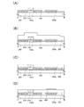
さらに、記憶回路の例について、図1を用いて説明する。 Further, an example of the memory circuit is described with reference to FIGS.
まず、本実施の形態の半導体装置における記憶回路の回路構成例について、図1(A)を
用いて説明する。
First, an example of a circuit configuration of the memory circuit in the semiconductor device of this embodiment is described with reference to FIG.
図1(A)に示す記憶回路は、トランジスタ111と、トランジスタ112と、を備える
。
The memory circuit illustrated in FIG. 1A includes a
なお、半導体装置において、トランジスタは、2つの端子と、印加される電圧により該2
つの端子の間に流れる電流を制御する電流制御端子と、を有する。なお、トランジスタに
限らず、素子において、互いの間に流れる電流が制御される端子を電流端子ともいい、2
つの電流端子のそれぞれを第1の電流端子及び第2の電流端子ともいう。
Note that in a semiconductor device, a transistor includes two terminals and a voltage applied to the transistor.
A current control terminal for controlling a current flowing between the two terminals. In addition, not only a transistor but the terminal in which the electric current which flows between each other in an element is controlled is also called a current terminal.
Each of the two current terminals is also referred to as a first current terminal and a second current terminal.
また、半導体装置において、トランジスタとしては、例えば電界効果トランジスタを用い
ることができる。電界効果トランジスタの場合、第1の電流端子は、ソース及びドレイン
の一方であり、第2の電流端子は、ソース及びドレインの他方であり、電流制御端子は、
ゲートである。
In the semiconductor device, for example, a field effect transistor can be used as the transistor. In the case of a field effect transistor, the first current terminal is one of a source and a drain, the second current terminal is the other of the source and the drain, and the current control terminal is
It is a gate.
また、一般的に電圧とは、ある二点間における電位の差(電位差ともいう)のことをいう
。しかし、電圧及び電位の値は、回路図などにおいていずれもボルト(V)で表されるこ
とがあるため、区別が困難である。そこで、本明細書では、特に指定する場合を除き、あ
る一点の電位と基準となる電位(基準電位ともいう)との電位差を、該一点の電圧として
用いる場合がある。
In general, a voltage refers to a difference in potential between two points (also referred to as a potential difference). However, the values of voltage and potential are both expressed in volts (V) in circuit diagrams and the like, and thus are difficult to distinguish. Therefore, in this specification, a potential difference between a potential at one point and a reference potential (also referred to as a reference potential) may be used as the voltage at the one point unless otherwise specified.
トランジスタ111は、ソース、ドレイン、第1のゲート、及び第2のゲートを有する。
第1のゲート又は第2のゲートの電圧により、トランジスタ111の閾値電圧(電圧Vt
hともいう)が制御される。例えば、トランジスタ111がN型トランジスタの場合、ト
ランジスタ111の第2のゲートの電圧が低くなるほど、トランジスタ111の閾値電圧
が正の方向にシフトする。
The
The threshold voltage (voltage Vt) of the
h)) is controlled. For example, in the case where the
トランジスタ111は、記憶回路にデータを入力するか否かを選択する選択トランジスタ
としての機能を有する。
The
トランジスタ111としては、例えばチャネルが形成される酸化物半導体層を含むトラン
ジスタを用いることができる。上記酸化物半導体層は、シリコンよりバンドギャップが高
く、真性(I型ともいう)、又は実質的に真性である半導体層であり、キャリアの数が極
めて少なく、キャリア濃度は、1×10¹⁴/cm3未満、好ましくは1×1012/c
m3未満、さらに好ましくは1×10¹¹/cm3未満である。
As the
It is less than m 3 , more preferably less than 1 × 10 11 / cm 3 .
また、上記酸化物半導体層を含むトランジスタのオフ電流は、チャネル幅1μmあたり1
0aA(1×10⁻¹⁷A)以下、好ましくはチャネル幅1μmあたり1aA(1×10
−18A)以下、さらには好ましくはチャネル幅1μmあたり10zA(1×10⁻²⁰
A)以下、さらに好ましくはチャネル幅1μmあたり1zA(1×10⁻²¹A)以下、
さらに好ましくはチャネル幅1μmあたり100yA(1×10⁻²²A)以下である。
The off-state current of the transistor including the oxide semiconductor layer is 1 per 1 μm of channel width.
0 aA (1 × 10 −17 A) or less, preferably 1 aA (1 × 10 7 per 1 μm channel width)
−18 A) or less, more preferably 10 zA per 1 μm channel width (1 × 10 −20
A) or less, more preferably 1 zA (1 × 10 −21 A) or less per channel width of 1 μm,
More preferably, it is 100 yA (1 × 10 −22 A) or less per 1 μm of channel width.
また、上記酸化物半導体層は、キャリア濃度が低いため、該酸化物半導体層を含むトラン
ジスタは、温度が変化した場合であっても、オフ電流が低い。例えばトランジスタの温度
が150℃であっても、オフ電流を、チャネル幅1μmあたり100zAとすることもで
きる。
In addition, since the oxide semiconductor layer has a low carrier concentration, a transistor including the oxide semiconductor layer has a low off-state current even when the temperature changes. For example, even when the transistor temperature is 150 ° C., the off-state current can be set to 100 zA per channel width of 1 μm.
また、上記酸化物半導体層としては、例えば層表面に垂直に配向(c軸配向ともいう)し
た結晶を含む酸化物半導体層を用いることもできる。例えば、基板温度を100℃以上5
00℃以下にして酸化物半導体膜を成膜し、その後加熱処理を行い、酸化物半導体層を形
成することにより、層表面に垂直に配向した結晶を含む酸化物半導体層を形成することが
できる。また、酸化物半導体層は複数の酸化物半導体層の積層であってもよい。上記層表
面に垂直に配向した結晶を含む酸化物半導体層を用いることにより、例えば光によるトラ
ンジスタの電気特性の変化を抑制することができる。
As the oxide semiconductor layer, for example, an oxide semiconductor layer including a crystal oriented perpendicularly to the layer surface (also referred to as c-axis orientation) can be used. For example, the substrate temperature is 100 ° C. or higher 5
By forming an oxide semiconductor film at a temperature lower than or equal to 00 ° C. and then performing heat treatment to form the oxide semiconductor layer, an oxide semiconductor layer including crystals oriented perpendicular to the layer surface can be formed. . The oxide semiconductor layer may be a stack of a plurality of oxide semiconductor layers. By using an oxide semiconductor layer including a crystal oriented perpendicular to the layer surface, for example, change in electrical characteristics of the transistor due to light can be suppressed.
トランジスタ112のゲートは、トランジスタ111のソース又はドレインに接続される
。
The gate of the
なお、本明細書において、2つ以上の構成要素が電気的に接続されていれば、該2つ以上
の構成要素が接続されているとみなすことができる。
Note that in this specification, if two or more components are electrically connected, it can be considered that the two or more components are connected.
トランジスタ112としては、例えばチャネルが形成され、元素周期表における第14族
の半導体(シリコンなど)を含有する半導体層を含むトランジスタを用いることができる
。
As the
次に、図1(A)に示す記憶回路の駆動方法例について説明する。 Next, an example of a method for driving the memory circuit illustrated in FIG. 1A will be described.
データを記憶回路に書き込む場合、まずトランジスタ111をオン状態にする。例えば、
トランジスタ111における第1のゲート電圧及び第2のゲート電圧を所定の値に設定す
ることにより、トランジスタ111をオン状態にすることができる。
When data is written to the memory circuit, the
By setting the first gate voltage and the second gate voltage of the
トランジスタ111がオン状態のとき、トランジスタ111のソース及びドレインを介し
てトランジスタ112のゲートにデータ信号が入力され、トランジスタ112のゲートの
電圧は、入力されるデータ信号の電圧と同等の値になる。
When the
その後、トランジスタ111をオフ状態にする。このとき、トランジスタ111のソース
及びドレインの間に流れる電流は、少ないほど好ましい。そこで、トランジスタ111の
第2のゲートの電圧を所定の値にし、トランジスタ111の閾値電圧を調整し、トランジ
スタ111がオフ状態のときにトランジスタ111のソース及びドレインの間に流れる電
流を極力少なくする。
After that, the
上記トランジスタ111の閾値電圧の調整例について、図1(B)を用いて説明する。
An example of adjusting the threshold voltage of the
図1(B)に示すように、例えばトランジスタ111の第2のゲートの電圧が接地電位G
NDと同等の値のとき、トランジスタ111の第1のゲート及びソースの間に印加される
電圧(電圧Vgsともいう)と、トランジスタ111のソース及びドレインの間に流れる
電流(電流Idともいう)との関係が曲線130で表されるとする。このとき、トランジ
スタ111の閾値電圧は、Vth_Aである。
As shown in FIG. 1B, for example, the voltage of the second gate of the
When the value is equal to ND, a voltage applied between the first gate and the source of the transistor 111 (also referred to as voltage Vgs) and a current flowing between the source and the drain of the transistor 111 (also referred to as current Id) Is represented by a
一方、トランジスタ111の第2のゲートの電圧を所定の値の電圧VAとしたとき、電圧
Vgsと電流Idとの関係は、曲線131で表すことができる。このとき、トランジスタ
111の閾値電圧は、電圧Vth_Aより正に大きい値の電圧Vth_Bである。
On the other hand, when the voltage of the second gate of the
以上のように、トランジスタ111の第2のゲートの電圧を調整することにより、トラン
ジスタ111の閾値電圧を調整することができる。
As described above, the threshold voltage of the
さらに、トランジスタ112のソース及びドレインの間の抵抗値は、トランジスタ112
のゲートの電圧に応じて決まる。よって、トランジスタ112のソース及びドレインの一
方の電圧を所定の値の電圧VBにしたときに、トランジスタ112のソース及びドレイン
の間に流れる電流に応じて設定されるトランジスタ112のソース及びドレインの他方の
電圧をデータとして記憶回路から読み出すこともできる。また、トランジスタ112のソ
ース及びドレインの他方の電圧をデータとして記憶回路から複数回読み出すこともできる
。
Further, the resistance value between the source and the drain of the
It depends on the gate voltage. Therefore, when the voltage of one of the source and the drain of the
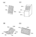
さらに、図1(A)に示す記憶回路の構造例について、図1(C)を用いて説明する。図
1(C)は、図1(A)に示す記憶回路の構造例を示す模式図である。なお、図1(C)
では、出力トランジスタがトップゲート型のトランジスタである場合について説明するが
、これに限定されず、出力トランジスタをボトムゲート型のトランジスタとしてもよい。
Further, a structural example of the memory circuit illustrated in FIG. 1A will be described with reference to FIG. FIG. 1C is a schematic diagram illustrating a structural example of the memory circuit illustrated in FIG. FIG. 1 (C)
Then, although the case where an output transistor is a top gate type transistor is demonstrated, it is not limited to this, An output transistor is good also as a bottom gate type transistor.
図1(C)に示す記憶回路は、半導体層152aと、半導体層152bと、絶縁層153
と、導電層154と、絶縁層155と、導電層157aと、導電層157bと、絶縁層1
58と、導電層159と、を含む。なお、必ずしも絶縁層155を設けなくてもよい。
A memory circuit illustrated in FIG. 1C includes a
58 and a
半導体層152a及び半導体層152bのそれぞれは、絶縁層151を介して基板150
の一平面に設けられる。
Each of the
Provided on one plane.
基板150としては、例えばガラス基板、石英基板、半導体基板、又はプラスチック基板
を用いることができる。
As the
絶縁層151としては、例えば酸化シリコン層、窒化シリコン層、酸化窒化シリコン層、
窒化酸化シリコン層、酸化アルミニウム層、窒化アルミニウム層、酸化窒化アルミニウム
層、窒化酸化アルミニウム層、又は酸化ハフニウム層を用いることができる。また、絶縁
層151に適用可能な材料の層の積層により絶縁層151を構成することもできる。
As the insulating
A silicon nitride oxide layer, an aluminum oxide layer, an aluminum nitride layer, an aluminum oxynitride layer, an aluminum nitride oxide layer, or a hafnium oxide layer can be used. Alternatively, the insulating
なお、絶縁層151に基板150からの不純物元素の拡散を防止する機能を付加させるこ
ともできる。
Note that the insulating
半導体層152aは、それぞれ不純物元素を含有する一対の不純物領域を有する。半導体
層152aは、一対の不純物領域の間にチャネル形成領域が設けられ、記憶回路における
出力トランジスタとしての機能を有するトランジスタのチャネルが形成される層(チャネ
ル形成層ともいう)としての機能を有する。不純物元素としては、N型の導電型を付与す
る不純物元素又はP型の導電型を付与する不純物元素が挙げられる。また、半導体層15
2aに不純物元素の濃度が異なる複数の不純物領域を設けてもよい。このとき、相対的に
不純物元素の濃度の低い領域を低濃度不純物領域という。低濃度不純物領域を設けること
により局所的な電界の集中を抑制することができる。
The
A plurality of impurity regions having different impurity element concentrations may be provided in 2a. At this time, a region having a relatively low impurity element concentration is referred to as a low concentration impurity region. By providing the low-concentration impurity region, local electric field concentration can be suppressed.
半導体層152aとしては、例えば非晶質半導体、微結晶半導体、多結晶半導体、又は単
結晶半導体を含む層を用いることができる。半導体層152aとしては、例えば元素周期
表における第14族の半導体(シリコンなど)を含有する半導体層を用いることができる
。
As the
半導体層152bは、不純物元素を含有する。不純物元素としては、N型の導電型を付与
する不純物元素又はP型の導電型を付与する不純物元素が挙げられる。半導体層152b
は、記憶回路における選択トランジスタとしての機能を有するトランジスタの第2のゲー
トとしての機能を有する。
The
Has a function as a second gate of a transistor having a function as a selection transistor in the memory circuit.
なお、トランジスタの第2のゲートとしての機能を有する導電層を第2のゲート電極又は
第2のゲート配線ともいう。
Note that the conductive layer functioning as the second gate of the transistor is also referred to as a second gate electrode or a second gate wiring.
半導体層152bとしては、半導体層152aと同じ材料の層を用いることができる。例
えば、絶縁層151の上に半導体層152a及び半導体層152bに適用可能な材料の半
導体層を形成する。さらに、上記半導体層の一部をエッチングすることにより、半導体層
152aとなる半導体層及び半導体層152bとなる半導体層を形成する。さらに、半導
体層152aとなる半導体層の一部、及び半導体層152bとなる半導体層に不純物元素
を添加することにより、同一工程で同一の膜から半導体層152a及び半導体層152b
を形成することができる。なお、半導体層152bは、導電型を付与する不純物元素を導
電層として機能できる程度に含むため、導電層とみなすことができる。
As the
Can be formed. Note that the
絶縁層153は、半導体層152a及び半導体層152bの上に設けられる。
The insulating
絶縁層153は、記憶回路における出力トランジスタとしての機能を有するトランジスタ
のゲート絶縁層としての機能を有する。
The insulating
絶縁層153としては、例えば絶縁層151に適用可能な材料の層、若しくはポリイミド
又はアクリルなどの有機絶縁材料などを用いることができる。また、絶縁層153に適用
可能な材料の層の積層により絶縁層153を構成してもよい。
As the insulating
なお、基板150として半導体基板を用いる場合には、絶縁層151、半導体層152a
、及び半導体層152bを設けずに、互いに絶縁分離され、半導体層152aに相当する
第1の半導体領域及び半導体層152bに相当する第2の半導体領域を含む半導体基板を
用い、第1の半導体領域及び第2の半導体領域の上に絶縁層153を形成してもよい。
Note that in the case where a semiconductor substrate is used as the
And a semiconductor substrate including a first semiconductor region corresponding to the
導電層154は、絶縁層153を介して半導体層152a(チャネル形成領域(一対の不
純物領域の間の領域)を含む)に重畳する。
The
導電層154は、記憶回路における出力トランジスタとしての機能を有するトランジスタ
のゲートとしての機能を有する。なお、トランジスタのゲートとしての機能を有する導電
層をゲート電極又はゲート配線ともいう。
The
導電層154としては、例えばモリブデン、チタン、クロム、タンタル、タングステン、
アルミニウム、銅、ネオジム、若しくはスカンジウムなどの金属材料を含む材料の層を用
いることができる。また、導電層154に適用可能な材料の層の積層により、導電層15
4を構成することもできる。
As the
A layer of a material containing a metal material such as aluminum, copper, neodymium, or scandium can be used. In addition, by stacking layers of materials applicable to the
4 can also be configured.
絶縁層155は、絶縁層153の上に設けられる。絶縁層155を設けることにより、例
えば導電層154による段差を平坦化することができ、上部への層の形成が容易になる。
The insulating
絶縁層155としては、例えば絶縁層151に適用可能な材料の層を用いることができる
。また、絶縁層155に適用可能な材料の層の積層により絶縁層155を構成してもよい
。
As the insulating
半導体層156は、絶縁層153及び絶縁層155を介して半導体層152bに重畳する
。
The
半導体層156は、記憶回路における選択トランジスタとしての機能を有するトランジス
タのチャネル形成層としての機能を有する。
The
半導体層156としては、例えばIn系酸化物、Sn系酸化物、又はZn系酸化物などを
用いることができる。上記金属酸化物としては、例えば四元系金属酸化物、三元系金属酸
化物、又は二元系金属酸化物などを用いることができる。なお、上記酸化物半導体として
適用可能な金属酸化物は、特性のばらつきを減らすためのスタビライザーとしてガリウム
を含んでいてもよい。また、上記酸化物半導体として適用可能な金属酸化物は、上記スタ
ビライザーとしてスズを含んでいてもよい。また、上記酸化物半導体として適用可能な金
属酸化物は、上記スタビライザーとしてハフニウムを含んでいてもよい。また、上記酸化
物半導体として適用可能な金属酸化物は、上記スタビライザーとしてアルミニウムを含ん
でいてもよい。また、上記酸化物半導体として適用可能な金属酸化物は、上記スタビライ
ザーとして、ランタノイドである、ランタン、セリウム、プラセオジム、ネオジム、サマ
リウム、ユウロピウム、ガドリニウム、テルビウム、ジスプロシウム、ホルミウム、エル
ビウム、ツリウム、イッテルビウム、及びルテチウムの一つ又は複数を含んでいてもよい
。また、上記酸化物半導体として適用可能な金属酸化物は、酸化シリコンを含んでいても
よい。四元系金属酸化物としては、例えばIn−Sn−Ga−Zn系酸化物、In−Hf
−Ga−Zn系酸化物、In−Al−Ga−Zn系酸化物、In−Sn−Al−Zn系酸
化物、In−Sn−Hf−Zn系酸化物、又はIn−Hf−Al−Zn系酸化物などを用
いることができる。三元系金属酸化物としては、例えばIn−Ga−Zn系酸化物(IG
ZOともいう)、In−Sn−Zn系酸化物(ITZOともいう)、In−Al−Zn系
酸化物、Sn−Ga−Zn系酸化物、Al−Ga−Zn系酸化物、Sn−Al−Zn系酸
化物、はIn−Hf−Zn系酸化物、In−La−Zn系酸化物、In−Ce−Zn系酸
化物、In−Pr−Zn系酸化物、In−Nd−Zn系酸化物、In−Sm−Zn系酸化
物、In−Eu−Zn系酸化物、In−Gd−Zn系酸化物、In−Tb−Zn系酸化物
、In−Dy−Zn系酸化物、In−Ho−Zn系酸化物、In−Er−Zn系酸化物、
In−Tm−Zn系酸化物、In−Yb−Zn系酸化物、又はIn−Lu−Zn系酸化物
などを用いることができる。二元系金属酸化物としては、例えばIn−Zn系酸化物(I
ZOともいう)、Sn−Zn系酸化物、Al−Zn系酸化物、Zn−Mg系酸化物、Sn
−Mg系酸化物、In−Mg系酸化物、In−Sn系酸化物、又はIn−Ga系酸化物な
どを用いることができる。
As the
-Ga-Zn oxide, In-Al-Ga-Zn oxide, In-Sn-Al-Zn oxide, In-Sn-Hf-Zn oxide, or In-Hf-Al-Zn oxide An oxide or the like can be used. As the ternary metal oxide, for example, an In—Ga—Zn oxide (IG
ZO), In—Sn—Zn-based oxide (also referred to as ITZO), In—Al—Zn-based oxide, Sn—Ga—Zn-based oxide, Al—Ga—Zn-based oxide, Sn—Al— Zn-based oxide, In-Hf-Zn-based oxide, In-La-Zn-based oxide, In-Ce-Zn-based oxide, In-Pr-Zn-based oxide, In-Nd-Zn-based oxide In-Sm-Zn-based oxide, In-Eu-Zn-based oxide, In-Gd-Zn-based oxide, In-Tb-Zn-based oxide, In-Dy-Zn-based oxide, In-Ho- Zn-based oxide, In-Er-Zn-based oxide,
An In—Tm—Zn-based oxide, an In—Yb—Zn-based oxide, an In—Lu—Zn-based oxide, or the like can be used. As the binary metal oxide, for example, an In—Zn oxide (I
ZO), Sn—Zn-based oxide, Al—Zn-based oxide, Zn—Mg-based oxide, Sn
-Mg-based oxide, In-Mg-based oxide, In-Sn-based oxide, In-Ga-based oxide, or the like can be used.
In−Zn−O系金属酸化物を用いる場合、例えば、In:Zn=50:1乃至In:Z
n=1:2(モル数比に換算するとIn2O3:ZnO=25:1乃至In2O3:Zn
O=1:4)、好ましくはIn:Zn=20:1乃至In:Zn=1:1(モル数比に換
算するとIn2O3:ZnO=10:1乃至In2O3:ZnO=1:2)、さらに好ま
しくはIn:Zn=15:1乃至In:Zn=1.5:1(モル数比に換算するとIn2
O3:ZnO=15:2乃至In2O3:ZnO=3:4)の組成比である酸化物ターゲ
ットを用いてIn−Zn−O系金属酸化物の半導体層を形成することができる。例えば、
In−Zn−O系酸化物半導体の形成に用いるターゲットは、原子数比がIn:Zn:O
=P:Q:Rのとき、R>1.5P+Qとする。Inの量を多くすることにより、トラン
ジスタの移動度を向上させることができる。
In the case of using an In—Zn—O-based metal oxide, for example, In: Zn = 50: 1 to In: Z
n = 1: 2 (In 2 O 3 : ZnO = 25: 1 to In 2 O 3 : Zn in terms of molar ratio)
O = 1: 4), preferably In: Zn = 20: 1 to In: Zn = 1: 1 (in terms of molar ratio, In 2 O 3 : ZnO = 10: 1 to In 2 O 3 : ZnO = 1 : 2), more preferably In: Zn = 15: 1 to In: Zn = 1.5: 1 (when converted to molar ratio, In 2
An In—Zn—O-based metal oxide semiconductor layer can be formed using an oxide target having a composition ratio of O 3 : ZnO = 15: 2 to In 2 O 3 : ZnO = 3: 4. For example,
A target used for forming an In—Zn—O-based oxide semiconductor has an atomic ratio of In: Zn: O.
When P = Q: R, R> 1.5P + Q. By increasing the amount of In, the mobility of the transistor can be improved.
また、酸化物半導体としては、InLO3(ZnO)m(mは0より大きい数)で表記さ
れる材料を用いることもできる。InLO3(ZnO)mのLは、Ga、Al、Mn、及
びCoから選ばれた一つ又は複数の金属元素を示す。
As the oxide semiconductor, a material represented by InLO 3 (ZnO) m (m is larger than 0) can be used. L in InLO 3 (ZnO) m represents one or more metal elements selected from Ga, Al, Mn, and Co.
導電層157aは、半導体層156に電気的に接続される。
The
導電層157aは、記憶回路における選択トランジスタとしての機能を有するトランジス
タのソース及びドレインの一方としての機能を有する。なお、トランジスタのソースとし
ての機能を有する導電層をソース電極又はソース配線ともいい、トランジスタのドレイン
としての機能を有する導電層をドレイン電極又はドレイン配線ともいう。
The
導電層157aとしては、例えばアルミニウム、クロム、銅、タンタル、チタン、モリブ
デン、若しくはタングステンなどの金属材料を含む層を用いることができる。
As the
また、導電層157aとしては、導電性の金属酸化物を含む層を用いることもできる。導
電性の金属酸化物としては、例えば酸化インジウム(In2O3)、酸化スズ(SnO2
)、酸化亜鉛(ZnO)、酸化インジウム酸化スズ合金(In2O3―SnO2、ITO
と略記する場合がある)、酸化インジウム酸化亜鉛合金(In2O3―ZnO)などの金
属酸化物、又はシリコン、酸化シリコン、窒素を含む該金属酸化物を用いることができる
。また、導電層157aに適用可能な材料の層の積層により、導電層157aを構成する
こともできる。
Alternatively, the
), Zinc oxide (ZnO), indium tin oxide alloy (In 2 O 3 —SnO 2 , ITO
Or a metal oxide such as indium oxide-zinc oxide alloy (In 2 O 3 —ZnO), or a metal oxide containing silicon, silicon oxide, or nitrogen can be used. Alternatively, the
導電層157bは、導電層154及び半導体層156に電気的に接続される。
The
なお、図1(C)では、導電層157bが導電層154に接している。必ずしもこれに限
定されないが、導電層157bが導電層154に接する構造にすることにより、開口部を
有する絶縁層の開口部を介して導電層157bが導電層154に電気的に接続される場合
と比較してコンタクト面積を大きくすることができるため、コンタクト抵抗を低減するこ
とができる。
Note that in FIG. 1C, the
導電層157bは、記憶回路における選択トランジスタとしての機能を有するトランジス
タのソース及びドレインの他方としての機能を有する。
The
導電層157bとしては、例えば導電層157aと同じ材料の層を用いることができる。
また、導電層157aに適用可能な材料の層の積層により、導電層157bを構成するこ
ともできる。
As the
Alternatively, the
例えば、導電層154、絶縁層155、及び半導体層156の上に、導電層157a及び
導電層157bに適用可能な材料の導電層を形成する。さらに、上記導電層の一部をエッ
チングすることにより、同一工程で同一の層から導電層157a及び導電層157bを形
成することができる。
For example, a conductive layer formed using a material that can be used for the
絶縁層158は、半導体層156、導電層157a、及び導電層157bの上に設けられ
る。
The insulating
絶縁層158は、記憶回路における選択トランジスタとしての機能を有するトランジスタ
のゲート絶縁層としての機能を有する。
The insulating
絶縁層158としては、絶縁層151に適用可能な材料の層を用いることができる。また
、絶縁層151に適用可能な材料の層の積層により、絶縁層158を構成することもでき
る。
As the insulating
また、絶縁層158としては、元素周期表における第13族元素及び酸素元素を含む材料
の絶縁層を用いることもできる。半導体層156が第13族元素を含む場合に、半導体層
156に接する絶縁層として第13族元素を含む絶縁層を用いることにより、該絶縁層と
酸化物半導体層との界面の状態を良好にすることができる。
As the insulating
第13族元素及び酸素元素を含む材料としては、例えば酸化ガリウム、酸化アルミニウム
、酸化アルミニウムガリウム、酸化ガリウムアルミニウムなどが挙げられる。なお、酸化
アルミニウムガリウムとは、ガリウムの含有量(原子%)よりアルミニウムの含有量(原
子%)が多い物質のことをいい、酸化ガリウムアルミニウムとは、ガリウムの含有量(原
子%)がアルミニウムの含有量(原子%)以上の物質のことをいう。例えば、AlOx(
x=3+α、αは0より大きく1より小さい値)、GaOx、又はGaXAl2−XO3
+α(Xは0より大きく2より小さい値、αは0より大きく1より小さい値)で表記され
る材料を用いることもできる。
Examples of the material containing a Group 13 element and an oxygen element include gallium oxide, aluminum oxide, aluminum gallium oxide, and gallium aluminum oxide. Aluminum gallium oxide refers to a substance having an aluminum content (atomic%) higher than the gallium content (atomic%), and gallium aluminum oxide refers to an aluminum gallium oxide (atomic%) containing aluminum. A substance with a content (atomic%) or more. For example, AlO x (
x = 3 + α, α is greater than 0 and less than 1), GaO x , or Ga X Al 2 -X O 3
A material represented by + α (X is a value greater than 0 and less than 2 and α is a value greater than 0 and less than 1) can also be used.
例えば、絶縁層158として、酸化ガリウムを含む絶縁層を用いることにより、絶縁層1
58と、半導体層156との界面における水素又は水素イオンの蓄積を低減することがで
きる。
For example, by using an insulating layer containing gallium oxide as the insulating
58 and accumulation of hydrogen or hydrogen ions at the interface between the
また、例えば、絶縁層158として、酸化アルミニウムを含む絶縁層を用いることにより
、絶縁層158と、半導体層156との界面における水素又は水素イオンの蓄積を低減す
ることができる。また、酸化アルミニウムを含む絶縁層は、水が通りにくいため、酸化ア
ルミニウムを含む絶縁層を用いることにより、該絶縁層を介して酸化物半導体層への水の
侵入を抑制することができる。
Further, for example, by using an insulating layer containing aluminum oxide as the insulating
また、例えば、複数のGaOxで表記される酸化ガリウムを含む層の積層により絶縁層1
58を構成してもよい。また、GaOxで表記される酸化ガリウムを含む絶縁層及びAl
Oxで表記される酸化アルミニウムを含む絶縁層の積層により絶縁層158を構成しても
よい。
Further, for example, the insulating
58 may be configured. An insulating layer containing gallium oxide represented by GaO x and Al
The insulating
導電層159は、絶縁層158を介して半導体層156に重畳する。
The
導電層159は、記憶回路における選択トランジスタとしての機能を有するトランジスタ
の第1のゲートとしての機能を有する。なお、トランジスタの第1のゲートとしての機能
を有する導電層を第1のゲート電極又は第1のゲート配線ともいう。
The
導電層159としては、導電層157aに適用可能な材料の層を用いることができる。ま
た、導電層159に適用可能な材料の層の積層により、導電層159を構成してもよい。
以上が図1(A)に示す記憶回路の構造例である。
As the
The above is the structural example of the memory circuit illustrated in FIG.
図1を用いて説明したように、本実施の形態における半導体装置の一例は、記憶回路を具
備する構成である。
As described with reference to FIG. 1, an example of the semiconductor device in this embodiment has a structure including a memory circuit.
さらに、本実施の形態における半導体装置の一例の上記記憶回路は、電界効果トランジス
タである選択トランジスタ及び出力トランジスタを少なくとも備える構成である。
Further, the memory circuit as an example of the semiconductor device in this embodiment includes at least a selection transistor and an output transistor that are field-effect transistors.
さらに、本実施の形態における半導体装置の一例の上記記憶回路において、選択トランジ
スタは、第1のゲートと、第2のゲートと、を有する構成である。
Further, in the memory circuit of the example of the semiconductor device in this embodiment, the selection transistor includes a first gate and a second gate.
さらに、本実施の形態における半導体装置の一例の上記記憶回路は、選択トランジスタに
おける第2のゲートとしての機能を有し、出力トランジスタのチャネル形成層としての機
能を有する半導体層と離間し、該半導体層と同じ材料である導電層を含む構成である。
Further, the memory circuit as an example of the semiconductor device in this embodiment has a function as a second gate of the selection transistor and is separated from a semiconductor layer having a function as a channel formation layer of the output transistor. The structure includes a conductive layer which is the same material as the layer.
上記構成にすることにより、必要に応じて選択トランジスタの閾値電圧を調整し、オフ状
態における選択トランジスタのソース及びドレインの間に流れる電流を極力小さくするこ
とができる。よって、記憶回路におけるデータの保持期間を長くすることができる。
With the above structure, the threshold voltage of the selection transistor can be adjusted as necessary, and the current flowing between the source and drain of the selection transistor in the off state can be minimized. Thus, the data retention period in the memory circuit can be extended.
また、上記構成にすることにより、データの書き込み及び読み出しに必要な電圧を従来の
半導体装置より低くすることができるため、消費電力を低減することができる。
Further, with the above structure, a voltage required for writing and reading data can be made lower than that of a conventional semiconductor device, so that power consumption can be reduced.
また、上記構成にすることにより、出力トランジスタのゲートにデータ信号を入力してデ
ータを書き込むことができるため、データの書き込み可能回数を増やすことができる。
Further, with the above structure, data can be written by inputting a data signal to the gate of the output transistor, so that the number of times data can be written can be increased.
また、上記構成にすることにより、同一工程で同一の材料の層を用いて出力トランジスタ
のチャネル形成層としての機能を有する半導体層と、選択トランジスタの第2のゲートと
しての機能を有する導電層を同時に形成することができるため、作製工程数の増加を抑制
することができ、製造コストの増加を抑制することができる。
In addition, with the above structure, a semiconductor layer having a function as a channel formation layer of an output transistor and a conductive layer having a function as a second gate of a selection transistor can be formed using layers of the same material in the same process. Since they can be formed at the same time, an increase in the number of manufacturing steps can be suppressed, and an increase in manufacturing cost can be suppressed.
(実施の形態2)
本実施の形態では、上記実施の形態における半導体装置の一例として、NOR型の半導体
記憶装置の例について説明する。
(Embodiment 2)
In this embodiment, an example of a NOR type semiconductor memory device will be described as an example of the semiconductor device in the above embodiment.
本実施の形態における半導体記憶装置の例は、I行(Iは2以上の自然数)J列(Jは自
然数)にマトリクス状に配列された複数のメモリセルを備えたメモリセルアレイを具備す
る。メモリセルは、上記実施の形態の半導体装置における記憶回路に相当する。
The example of the semiconductor memory device in this embodiment includes a memory cell array including a plurality of memory cells arranged in a matrix in I rows (I is a natural number of 2 or more) J columns (J is a natural number). The memory cell corresponds to the memory circuit in the semiconductor device of the above embodiment.
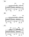
さらに、本実施の形態の半導体記憶装置におけるメモリセルアレイの例について、図2を
用いて説明する。
Further, an example of a memory cell array in the semiconductor memory device of this embodiment is described with reference to FIG.
まず、本実施の形態の半導体記憶装置におけるメモリセルアレイの回路構成例について、
図2(A)を用いて説明する。
First, regarding a circuit configuration example of a memory cell array in the semiconductor memory device of the present embodiment,
This will be described with reference to FIG.
図2(A)に示すメモリセルアレイは、i行(iは3以上の自然数)j列(jは3以上の
自然数)のマトリクス状に配列された複数のメモリセル200と、i本のワード線WL(
ワード線WL_1乃至ワード線WL_i)と、i本の容量線CL(容量線CL_1乃至容
量線CL_i)と、i本のゲート線BGL(ゲート線BGL_1乃至ゲート線BGL_i
)と、j本のビット線BL(ビット線BL_1乃至ビット線BL_j)と、ソース線SL
と、を具備する。
A memory cell array shown in FIG. 2A includes a plurality of
Word line WL_1 to word line WL_i), i capacitance lines CL (capacitance lines CL_1 to capacitance lines CL_i), and i gate lines BGL (gate lines BGL_1 to gate lines BGL_i).
), J bit lines BL (bit lines BL_1 to BL_j), and source lines SL
And.
さらに、M(Mはi以下の自然数)行N(Nはj以下の自然数)列目のメモリセル200
(メモリセル200(M,N)ともいう)は、トランジスタ211(M,N)と、容量素
子213(M,N)と、トランジスタ212(M,N)と、を備える。
Further, the
The memory cell 200 (also referred to as a memory cell 200 (M, N)) includes a transistor 211 (M, N), a capacitor 213 (M, N), and a transistor 212 (M, N).
なお、半導体記憶装置において、容量素子は、第1の容量電極、第2の容量電極、並びに
第1の容量電極及び第2の容量電極に重畳する誘電体層により構成される。容量素子は、
第1の容量電極及び第2の容量電極の間に印加される電圧に応じて電荷が蓄積される。
Note that in the semiconductor memory device, the capacitor element includes a first capacitor electrode, a second capacitor electrode, and a dielectric layer overlapping with the first capacitor electrode and the second capacitor electrode. Capacitance element is
Charges are accumulated according to the voltage applied between the first capacitor electrode and the second capacitor electrode.
トランジスタ211(M,N)は、Nチャネル型トランジスタであり、ソース、ドレイン
、第1のゲート、及び第2のゲートを有する。なお、本実施の形態の半導体記憶装置にお
いて、必ずしもトランジスタ211をNチャネル型トランジスタにしなくてもよい。
The transistor 211 (M, N) is an N-channel transistor and includes a source, a drain, a first gate, and a second gate. Note that in the semiconductor memory device in this embodiment, the
トランジスタ211(M,N)のソース及びドレインの一方は、ビット線BL_Nに接続
され、トランジスタ211(M,N)の第1のゲートは、ワード線WL_Mに接続され、
トランジスタ211(M,N)の第2のゲートは、ゲート線BGL_Mに接続される。ト
ランジスタ211(M,N)のソース及びドレインの一方がビット線BL_Nに接続され
る構成にすることにより、1個以上のメモリセルから選択的にデータを読み出すことがで
きる。
One of a source and a drain of the transistor 211 (M, N) is connected to the bit line BL_N, and a first gate of the transistor 211 (M, N) is connected to the word line WL_M.
A second gate of the transistor 211 (M, N) is connected to the gate line BGL_M. With the structure in which one of the source and the drain of the transistor 211 (M, N) is connected to the bit line BL_N, data can be selectively read from one or more memory cells.
トランジスタ211(M,N)は、メモリセル200(M,N)において選択トランジス
タとしての機能を有する。
The transistor 211 (M, N) functions as a selection transistor in the memory cell 200 (M, N).
トランジスタ211(M,N)としては、例えば上記実施の形態1の半導体装置における
トランジスタ111に適用可能な酸化物半導体層を含むトランジスタを用いることができ
る。
As the transistor 211 (M, N), for example, a transistor including an oxide semiconductor layer that can be used as the
トランジスタ212(M,N)は、Pチャネル型トランジスタである。なお、本実施の形
態の半導体記憶装置において、必ずしもトランジスタ212をPチャネル型トランジスタ
にしなくてもよい。
The transistor 212 (M, N) is a P-channel transistor. Note that in the semiconductor memory device in this embodiment, the
トランジスタ212(M,N)のソース及びドレインの一方は、ソース線SLに接続され
、トランジスタ212(M,N)のソース及びドレインの他方は、ビット線BL_Nに接
続され、トランジスタ212(M,N)のゲートは、トランジスタ212(M,N)のソ
ース及びドレインの他方に接続される。
One of a source and a drain of the transistor 212 (M, N) is connected to the source line SL, and the other of the source and the drain of the transistor 212 (M, N) is connected to the bit line BL_N, and the transistor 212 (M, N ) Is connected to the other of the source and the drain of the transistor 212 (M, N).
トランジスタ212(M,N)は、メモリセル200(M,N)において、出力トランジ
スタとしての機能を有する。
The transistor 212 (M, N) functions as an output transistor in the memory cell 200 (M, N).
トランジスタ212(M,N)としては、上記実施の形態1の半導体装置におけるトラン
ジスタ112に適用可能な第14族の半導体(シリコンなど)を含有する半導体層を含む
トランジスタを用いることができる。
As the transistor 212 (M, N), a transistor including a semiconductor layer containing a Group 14 semiconductor (such as silicon) applicable to the
容量素子213(M,N)の第1の容量電極は、容量線CL_Mに接続され、容量素子2
13(M,N)の第2の容量電極は、トランジスタ211(M,N)のソース及びドレイ
ンの他方に接続される。
A first capacitor electrode of the capacitor 213 (M, N) is connected to the capacitor line CL_M, and the
The 13th (M, N) second capacitor electrode is connected to the other of the source and the drain of the transistor 211 (M, N).
容量素子213(M,N)は、保持容量としての機能を有する。 The capacitor 213 (M, N) functions as a storage capacitor.
ワード線WL_1乃至ワード線WL_iのそれぞれの電圧は、例えばデコーダを用いた駆
動回路により制御される。
Each voltage of the word lines WL_1 to WL_i is controlled by, for example, a driving circuit using a decoder.
ビット線BL_1乃至ビット線BL_jのそれぞれの電圧は、例えばデコーダを用いた駆
動回路により制御される。
Each voltage of the bit lines BL_1 to BL_j is controlled by, for example, a driver circuit using a decoder.
容量線CL_1乃至容量線CL_iのそれぞれの電圧は、例えばデコーダを用いた駆動回
路により制御される。
The voltages of the capacitor lines CL_1 to CL_i are controlled by a driving circuit using a decoder, for example.
ゲート線BGL_1乃至ゲート線BGL_iのそれぞれの電圧は、例えばゲート線駆動回
路を用いて制御される。
Each voltage of the gate lines BGL_1 to BGL_i is controlled using, for example, a gate line driver circuit.
ゲート線駆動回路は、例えばダイオード及び容量素子を備える回路により構成される。こ
のとき、上記容量素子の第1の容量電極は、上記ダイオードのアノード及びゲート線BG
Lに電気的に接続される。
The gate line driving circuit is configured by a circuit including a diode and a capacitor, for example. At this time, the first capacitor electrode of the capacitor element includes the anode of the diode and the gate line BG.
L is electrically connected.
さらに、図2(A)に示すメモリセルアレイの駆動方法例について、図2(B)を用いて
説明する。図2(B)は、図2(A)に示すメモリセルアレイの駆動方法例を説明するた
めのタイミングチャートである。ここでは、一例として1行1列目のメモリセル200(
1,1)と2行2列目のメモリセル200(2,2)に順次データを書き込み、その後書
き込まれたデータを読み出す場合について説明する。なお、図2(B)に示すタイミング
チャートの中で、電圧Vhは、トランジスタ211の閾値電圧より大きい電圧であり、ま
た斜線部は、電圧が電圧Vh又は接地電位GNDと同等の値のいずれの場合でもよい部分
である。
Further, an example of a method for driving the memory cell array illustrated in FIG. 2A will be described with reference to FIG. FIG. 2B is a timing chart for explaining an example of a method for driving the memory cell array illustrated in FIG. Here, as an example, the
1, 1) and 2nd row and 2nd column memory cell 200 (2, 2) are sequentially written, and then the written data is read. Note that in the timing chart shown in FIG. 2B, the voltage Vh is higher than the threshold voltage of the
まず、図2(B)における期間t21に示すように、ワード線WL_1の電圧を電圧Vh
にする。このとき、容量線CL_1の電圧を接地電位GNDと同等の値にする。また、ワ
ード線WL_1以外のワード線WLの電圧を基準電位である接地電位GNDと同等の値に
し、容量線CL_1以外の容量線CLの電圧を電圧Vhにする。また、ソース線SLの電
圧を接地電位GNDと同等の値にする。
First, as shown in a period t21 in FIG. 2B, the voltage of the word line WL_1 is set to the voltage Vh.
To. At this time, the voltage of the capacitor line CL_1 is set to a value equivalent to the ground potential GND. Further, the voltage of the word line WL other than the word line WL_1 is set to a value equivalent to the ground potential GND which is the reference potential, and the voltage of the capacitor line CL other than the capacitor line CL_1 is set to the voltage Vh. Further, the voltage of the source line SL is set to a value equivalent to the ground potential GND.
このとき、1行目のメモリセル200(メモリセル200(1,1)乃至メモリセル20
0(1,j))において、トランジスタ211(1,1)乃至トランジスタ211(1,
j)がオン状態になる。
At this time, the
0 (1, j)), the transistors 211 (1,1) to 211 (1,1)
j) is turned on.
トランジスタ211(1,1)乃至トランジスタ211(1,j)がオン状態のとき、ト
ランジスタ211(1,1)を介してビット線BL_1からトランジスタ212(1,1
)のゲート及び容量素子213(1,1)の第2の容量電極にメモリデータ信号が入力さ
れる。このとき、トランジスタ212(1,1)のゲート及び容量素子213(1,1)
の第2の容量電極の電圧は、入力されるメモリデータ信号の電圧と同等の値になり、1行
1列目のメモリセル200(1,1)は、書き込み状態になる。ここでは、一例としてビ
ット線BL_1の電圧が接地電位GNDと同等の値であるとする。
When the transistors 211 (1, 1) to 211 (1, j) are on, the transistor 212 (1, 1) is connected to the bit line BL_1 through the transistor 211 (1, 1).
) And the second capacitor electrode of the capacitor 213 (1, 1). At this time, the gate of the transistor 212 (1,1) and the capacitor 213 (1,1)
The voltage of the second capacitor electrode is equal to the voltage of the input memory data signal, and the memory cell 200 (1, 1) in the first row and first column is in the write state. Here, as an example, the voltage of the bit line BL_1 is assumed to be equal to the ground potential GND.
1行1列目のメモリセル200(1,1)を含む1行目のメモリセル200にデータが書
き込まれた後、ワード線WL_1の電圧を接地電位GNDと同等の値にし、容量線CL_
1の電圧を例えば接地電位GNDのままにする。このとき、ワード線WL_1以外のワー
ド線WLの電圧は接地電位GNDと同等の値であり、容量線CL_1以外の容量線CLの
電圧を例えば電圧Vhのままにする。また、1行目のゲート線BGL_1の電圧をVlに
する。電圧Vlは、接地電位GND以下の値の電圧である。
After data is written in the
For example, the
このとき、トランジスタ211(1,1)乃至トランジスタ211(1,j)は、オフ状
態になる。さらに、トランジスタ211(1,1)乃至トランジスタ211(1,j)の
閾値電圧は、正の値になる。よって、容量素子213(1,1)乃至容量素子213(1
,j)の第2の容量電極の電圧及びトランジスタ212(1,1)乃至トランジスタ21
2(1,j)のゲートの電圧は、一定期間保持される。
At this time, the transistors 211 (1, 1) to 211 (1, j) are turned off. Further, the threshold voltages of the transistors 211 (1, 1) to 211 (1, j) are positive values. Therefore, the capacitor 213 (1,1) to the capacitor 213 (1
, J) of the second capacitor electrode and the transistors 212 (1, 1) to 21
The gate voltage of 2 (1, j) is held for a certain period.
次に、図2(B)における期間t22に示すように、ワード線WL_2の電圧を電圧Vh
にし、容量線CL_2の電圧を接地電位GNDと同等の値にする。このとき、ワード線W
L_2以外のワード線WLの電圧を接地電位GNDと同等の値にし、容量線CL_2以外
の容量線CLの電圧を電圧Vhにする。また、ソース線SLの電圧を接地電位GNDと同
等の値にする。
Next, as illustrated in a period t22 in FIG. 2B, the voltage of the word line WL_2 is set to the voltage Vh.
The voltage of the capacitor line CL_2 is set to a value equivalent to the ground potential GND. At this time, the word line W
The voltage of the word line WL other than L_2 is set to a value equivalent to the ground potential GND, and the voltage of the capacitor line CL other than the capacitor line CL_2 is set to the voltage Vh. Further, the voltage of the source line SL is set to a value equivalent to the ground potential GND.
このとき、2行目のメモリセル200(メモリセル200(2,1)乃至メモリセル20
0(2,j))において、トランジスタ211(2,1)乃至トランジスタ211(2,
j)がオン状態になる。
At this time, the memory cells 200 (memory cells 200 (2,1) to 20) in the second row
0 (2, j)), the transistors 211 (2,1) to 211 (2, j)
j) is turned on.
トランジスタ211(2,1)乃至トランジスタ211(2,j)がオン状態のとき、ト
ランジスタ211(2,2)を介してビット線BL_2からトランジスタ212(2,2
)のゲート及び容量素子213(2,2)の第2の容量電極にメモリデータ信号が入力さ
れる。このとき、トランジスタ212(2,2)のゲート及び容量素子213(2,2)
の第2の容量電極の電圧は、入力されるメモリデータ信号の電圧と同等の値になり、2行
2列目のメモリセル200(2,2)は、書き込み状態になる。ここでは、一例としてビ
ット線BL_2の電圧が接地電位GNDと同等の値であるとする。
When the transistors 211 (2, 1) to 211 (2, j) are on, the transistor 212 (2, 2) is connected from the bit line BL_2 through the transistor 211 (2, 2).
) And the second capacitor electrode of the capacitor 213 (2, 2). At this time, the gate of the transistor 212 (2, 2) and the capacitor 213 (2, 2)
The voltage of the second capacitor electrode is equal to the voltage of the input memory data signal, and the memory cell 200 (2, 2) in the second row and the second column is in the write state. Here, as an example, it is assumed that the voltage of the bit line BL_2 is equal to the ground potential GND.
2行1列目のメモリセル200(2,1)を含む2行目のメモリセル200にデータが書
き込まれた後、ワード線WL_2の電圧を接地電位GNDと同等の値にし、容量線CL_
2の電圧を例えば接地電位GNDと同等の値にする。このとき、ワード線WL_2以外の
ワード線WLの電圧は接地電位GNDと同等の値であり、容量線CL_2以外の容量線C
Lの電圧を例えば電圧Vhにする。また、ゲート線BGL_2の電圧をVlにする。また
、ビット線BL_1及びビットBL_2の電圧は、接地電位GNDと同等の値であるとす
る。
After data is written in the
For example, the voltage of 2 is set to a value equivalent to the ground potential GND. At this time, the voltages of the word lines WL other than the word line WL_2 are equal to the ground potential GND, and the capacitance lines C other than the capacitance line CL_2.
For example, the voltage L is set to the voltage Vh. Further, the voltage of the gate line BGL_2 is set to Vl. In addition, the voltages of the bit line BL_1 and the bit BL_2 are assumed to be equal to the ground potential GND.
このとき、トランジスタ211(2,1)乃至トランジスタ211(2,j)は、オフ状
態になる。さらに、トランジスタ211(2,1)乃至トランジスタ211(2,j)の
閾値電圧は、正の値になる。よって、容量素子213(2,1)乃至容量素子213(2
,j)の第2の容量電極の電圧及びトランジスタ212(2,1)乃至トランジスタ21
2(2,j)のゲートの電圧は、一定期間保持される。
At this time, the transistors 211 (2, 1) to 211 (2, j) are turned off. Further, the threshold voltages of the transistors 211 (2, 1) to 211 (2, j) are positive values. Therefore, the capacitor 213 (2,1) to the capacitor 213 (2
, J) of the second capacitor electrode and the transistors 212 (2, 1) to 21
The gate voltage of 2 (2, j) is held for a certain period.
さらに、図2(B)における期間t23に示すように、ソース線SLの電圧を電圧Vrに
し、容量線CL_1の電圧を接地電位GNDと同等の値にする。このとき、ワード線WL
_1乃至ワード線WL_iの電圧を接地電位GNDと同等の値にし、容量線CL_1以外
の容量線CLの電圧を電圧Vhにする。電圧Vrは、接地電位GND以上電圧Vh以下の
値の電圧である。
Further, as shown in a period t23 in FIG. 2B, the voltage of the source line SL is set to the voltage Vr, and the voltage of the capacitor line CL_1 is set to a value equivalent to the ground potential GND. At this time, the word line WL
_1 to the voltage of the word line WL_i are set to the same value as the ground potential GND, and the voltages of the capacitor lines CL other than the capacitor line CL_1 are set to the voltage Vh. The voltage Vr is a voltage having a value greater than or equal to the ground potential GND and less than or equal to the voltage Vh.
このとき、1行1列目のメモリセル200(1,1)において、トランジスタ212(1
,1)のソース及びドレインの間の抵抗値は、トランジスタ212(1,1)のゲートの
電圧に応じた値になる。よって、トランジスタ212(1,1)のゲートの電圧に応じた
値の電圧がデータとしてビット線BL_1を介して出力されることにより、メモリセル2
00(1,1)からデータが読み出される。
At this time, in the memory cell 200 (1, 1) in the first row and the first column, the transistor 212 (1
, 1) has a resistance value between the source and drain corresponding to the voltage of the gate of the transistor 212 (1, 1). Therefore, a voltage having a value corresponding to the gate voltage of the transistor 212 (1,1) is output as data through the bit line BL_1, whereby the
Data is read from 00 (1, 1).
次に、図2(B)における期間t24に示すように、ソース線SLの電圧を電圧Vrにし
、容量線CL_2の電圧を接地電位GNDと同等の値にする。このとき、ワード線WL_
1乃至ワード線WL_iの電圧を接地電位GNDと同等の値にし、容量線CL_2以外の
容量線CLの電圧を電圧Vhにする。
Next, as illustrated in a period t24 in FIG. 2B, the voltage of the source line SL is set to the voltage Vr, and the voltage of the capacitor line CL_2 is set to a value equivalent to the ground potential GND. At this time, the word line WL_
The voltages of the first to word lines WL_i are set to a value equivalent to the ground potential GND, and the voltages of the capacitor lines CL other than the capacitor line CL_2 are set to the voltage Vh.
このとき、2行2列目のメモリセル200(2,2)において、トランジスタ212(2
,2)のソース及びドレインの間の抵抗値は、トランジスタ212(2,2)のゲートの
電圧に応じた値になる。よって、トランジスタ212(2,2)のゲートの電圧に応じた
値の電圧がデータとしてビット線BL_1を介して出力されることにより、メモリセル2
00(2,2)からデータが読み出される。以上が図2(A)に示すメモリセルアレイの
駆動方法例である。
At this time, in the memory cell 200 (2, 2) in the second row and the second column, the transistor 212 (2
, 2) has a resistance value between the source and drain corresponding to the voltage of the gate of the transistor 212 (2, 2). Therefore, a voltage having a value corresponding to the gate voltage of the transistor 212 (2, 2) is output as data through the bit line BL_1, whereby the
Data is read from 00 (2, 2). The above is the example of the method for driving the memory cell array illustrated in FIG.
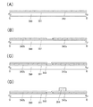
次に、図2(A)に示すメモリセルアレイにおけるメモリセル200の構造例について、
図3を用いて説明する。図3(A)は、上面図であり、図3(B)は、図3(A)におけ
る線分A−Bの断面図である。
Next, a structural example of the
This will be described with reference to FIG. 3A is a top view, and FIG. 3B is a cross-sectional view taken along line AB in FIG. 3A.
図3(A)及び図3(B)に示すメモリセルは、半導体層252aと、半導体層252b
と、絶縁層253と、導電層254と、絶縁層255と、半導体層256と、導電層25
7aと、導電層257bと、絶縁層258と、導電層259aと、導電層259bと、絶
縁層260と、導電層261と、を含む。なお、本実施の形態の半導体記憶装置において
、必ずしも絶縁層255を設けなくてもよい。
The memory cell illustrated in FIGS. 3A and 3B includes a
The insulating
7a,
半導体層252a及び半導体層252bは、絶縁層251を介して基板250の一平面に
設けられる。
The
基板250としては、上記実施の形態1に示す基板150に適用可能な基板を用いること
ができる。
As the
絶縁層251としては、例えば酸化絶縁層を用いることができ、例えば酸化シリコン層又
は酸化窒化シリコン層などを用いることができる。また、上記酸化絶縁層がハロゲンを含
んでいてもよい。なお、絶縁層251に適用可能な材料の層を積層することにより絶縁層
251を構成することもできる。
As the insulating
半導体層252aは、一対の不純物領域を有する。半導体層252aは、一対の不純物領
域の間にチャネル形成領域が設けられる。不純物元素としては、P型の導電型を付与する
不純物元素が挙げられるが、これに限定されず、N型の導電型を付与する不純物元素を用
いてよい。また、半導体層252aに不純物元素の濃度が異なる複数の不純物領域を設け
てもよい。このとき、相対的に不純物元素の濃度の低い領域を低濃度不純物領域という。
低濃度不純物領域を設けることにより局所的な電界の集中を抑制することができる。
The
By providing the low-concentration impurity region, local electric field concentration can be suppressed.
半導体層252aは、ソース線及び各メモリセルにおける出力トランジスタとしての機能
を有するトランジスタのチャネル形成層としての機能を有する。
The
半導体層252bは、半導体層252aにおける不純物領域と同じ不純物元素を含む。半
導体層252bは、半導体層252aと離間する。なお、半導体層252bは、導電型を
付与する不純物元素を導電層として機能できる程度に含むため、導電層とみなすことがで
きる。
The
半導体層252bは、ゲート線BGL及び各メモリセルにおける選択トランジスタとして
の機能を有するトランジスタの第2のゲートとしての機能を有する。
The
半導体層252a及び半導体層252bとしては、例えば上記実施の形態における半導体
層152a及び半導体層152bに適用可能な材料の層を用いることができる。
As the
絶縁層253は、半導体層252a及び半導体層252bの上に設けられる。
The insulating
絶縁層253は、各メモリセルにおける出力トランジスタとしての機能を有するトランジ
スタのゲート絶縁層としての機能を有する。
The insulating
絶縁層253としては、例えば上記実施の形態1における絶縁層151に適用可能な材料
の層を用いることができる。また、絶縁層253に適用可能な材料の層の積層により絶縁
層253を構成することもできる。
As the insulating
導電層254は、絶縁層253を介して半導体層252a(チャネル形成領域を含む)に
重畳する。なお、導電層254の側面をテーパにしてもよい。導電層254の側面をテー
パにすることにより、上部の層を形成しやすくすることができる。
The
導電層254は、メモリセルにおける出力トランジスタとしての機能を有するトランジス
タのゲートとしての機能を有する。
The
導電層254としては、上記実施の形態1における導電層154に適用可能な材料の層を
用いることができる。また、導電層254に適用可能な材料の層の積層により、導電層2
54を構成することもできる。
As the
54 can be configured.
絶縁層255は、絶縁層253の上に設けられる。絶縁層255を設けることにより、例
えば導電層254による段差を平坦化することができ、上部への層の形成が容易になる。
The insulating
絶縁層255としては、例えば上記実施の形態1における絶縁層151に適用可能な材料
の層を用いることができる。また、絶縁層255に適用可能な材料の層の積層により絶縁
層255を構成してもよい。例えば、酸化窒化シリコン層、窒化酸化シリコン層、及び酸
化シリコン層の積層により絶縁層255を構成することができる。
As the insulating
半導体層256は、絶縁層253及び絶縁層255を介して半導体層252bに重畳する
。
The
半導体層256は、メモリセルにおける選択トランジスタとしての機能を有するトランジ
スタのチャネル形成層としての機能を有する。
The
半導体層256としては、例えば上記実施の形態1における半導体層156に適用可能な
材料の層を用いることができる。
As the
導電層257aは、半導体層256に電気的に接続される。
The
導電層257aは、メモリセルにおける選択トランジスタとしての機能を有するトランジ
スタのソース及びドレインの一方としての機能を有する。
The
導電層257bは、導電層254及び半導体層256に電気的に接続される。また、導電
層257bが導電層254に接する構造にすることにより、開口部を有する絶縁層の該開
口部を介して導電層257bが導電層254に電気的に接続される場合と比較してコンタ
クト面積を大きくすることができるため、コンタクト抵抗を低減することができる。
The
導電層257bは、メモリセルにおける選択トランジスタとしての機能を有するトランジ
スタのソース及びドレインの他方、及びメモリセルにおける保持容量としての機能を有す
る容量素子の第2の容量電極としての機能を有する。
The
導電層257a及び導電層257bとしては、例えば上記実施の形態1における導電層1
57a及び導電層157bに適用可能な材料の層を用いることができる。また、導電層1
57a及び導電層157bに適用可能な材料の層の積層により、導電層257a及び導電
層257bを構成することもできる。
As the
A layer of a material applicable to 57a and the
The
絶縁層258は、半導体層256、導電層257a、及び導電層257bの上に設けられ
る。
The insulating
絶縁層258は、メモリセルにおける選択トランジスタとしての機能を有するトランジス
タのゲート絶縁層、及びメモリセルにおける保持容量としての機能を有する容量素子の誘
電体層としての機能を有する。
The insulating
絶縁層258としては、上記実施の形態1における絶縁層158に適用可能な材料の絶縁
層を用いることができる。また、絶縁層258に適用可能な材料の層の積層により絶縁層
258を構成することもできる。
As the insulating
導電層259aは、絶縁層258を介して導電層257bに重畳する。
The
導電層259aは、メモリセルにおける保持容量としての機能を有する容量素子の第1の
容量電極としての機能を有する。
The
導電層259bは、絶縁層258を介して半導体層256に重畳する。
The
導電層259bは、ワード線WL及びメモリセルにおける選択トランジスタとしての機能
を有するトランジスタの第1のゲートとしての機能を有する。
The
導電層259a及び導電層259bとしては、上記実施の形態1における導電層159に
適用可能な材料の層を用いることができる。また、導電層259a及び導電層259bに
適用可能な材料の層の積層により、導電層259a及び導電層259bを構成することも
できる。
As the
絶縁層260は、絶縁層258、導電層259a、及び導電層259bの上に設けられる
。
The insulating
絶縁層260としては、例えば絶縁層255に適用可能な材料の層を用いることができる
。また、絶縁層260に適用可能な材料の層の積層により絶縁層260を構成することも
できる。
As the insulating
導電層261は、絶縁層258、及び絶縁層260に設けられた開口部を介して導電層2
57aに接し、絶縁層253、絶縁層255、絶縁層258、及び絶縁層260に設けら
れた開口部を介して半導体層252aにおける一対の不純物領域の一方に接する。
The
57a is in contact with one of a pair of impurity regions in the
導電層261は、メモリセルにおけるビット線BLとしての機能を有する。
The
導電層261としては、例えば導電層254に適用可能な材料の層を用いることができる
。また、導電層261に適用可能な材料の層の積層により導電層261を構成することも
できる。
As the
また、導電層261の上に絶縁層を設け、該絶縁層の上に、該絶縁層に設けられた開口部
を介して導電層261に電気的に接続された別の導電層を設けてもよい。
Alternatively, an insulating layer may be provided over the
なお、本実施の形態の半導体記憶装置におけるメモリセルでは、必要に応じて選択トラン
ジスタとしての機能を有するトランジスタの閾値電圧を所望の値にシフトさせることがで
きるように、第2のゲートに印加される電圧の値又は絶縁層255の膜厚が適宜設定され
る。
Note that in the memory cell in the semiconductor memory device of this embodiment, the threshold voltage of the transistor having a function as a selection transistor is applied to the second gate so that the threshold voltage can be shifted to a desired value as necessary. The voltage value or the film thickness of the insulating
次に、図3に示すメモリセルの作製方法例について、図4乃至図7を用いて説明する。図
4乃至図7は、図3に示すメモリセルの作製方法例を示す断面図である。
Next, an example of a method for manufacturing the memory cell illustrated in FIG. 3 will be described with reference to FIGS. 4 to 7 are cross-sectional views illustrating an example of a method for manufacturing the memory cell illustrated in FIG.
まず、図4(A)に示すように、基板250を準備し、基板250の一平面に絶縁層25
1を形成し、絶縁層251を介して基板250の一平面に半導体層242を形成する。な
お、予め基板250の上に酸化絶縁層又は窒化絶縁層を形成してもよい。
First, as shown in FIG. 4A, a
1 is formed, and a
基板250の一平面に絶縁層251及び半導体層242を形成する例について以下に説明
する。
An example in which the insulating
例えば、基板250と、上面に絶縁層251を形成した半導体基板を準備する。
For example, a
例えば、熱酸化法、CVD法、又はスパッタリング法などにより、酸化物絶縁膜を形成す
ることにより、酸化物絶縁層を形成することができる。例えば、熱酸化法における熱酸化
処理により上記半導体基板の上に酸化シリコン膜を形成することにより酸化物絶縁層を形
成することができる。
For example, the oxide insulating layer can be formed by forming an oxide insulating film by a thermal oxidation method, a CVD method, a sputtering method, or the like. For example, an oxide insulating layer can be formed by forming a silicon oxide film over the semiconductor substrate by a thermal oxidation process in a thermal oxidation method.
さらに、半導体基板に電界で加速されたイオンでなるイオンビームを注入し、該半導体基
板の表面から一定の深さの領域に、脆化領域を形成する。なお、イオンの運動エネルギー
、イオンの質量と電荷、イオンの入射角などを調節することにより上記脆化領域の深さを
調節する。
Further, an ion beam made of ions accelerated by an electric field is implanted into the semiconductor substrate, and an embrittled region is formed in a region having a certain depth from the surface of the semiconductor substrate. Note that the depth of the embrittlement region is adjusted by adjusting ion kinetic energy, ion mass and charge, ion incident angle, and the like.
例えば、イオンドーピング装置又はイオン注入装置を用いて上記半導体基板にイオンを注
入することができる。
For example, ions can be implanted into the semiconductor substrate using an ion doping apparatus or an ion implantation apparatus.
また、注入するイオンとしては、例えば水素又はヘリウムの一つ又は複数を用いることが
できる。例えば、イオンドーピング装置を用いて水素イオンを注入する場合、注入するイ
オンにおいて、H3 +の比率を高くすることにより、イオン注入の効率を高めることがで
きる。具体的には、H+、H2 +、H3 +の総量に対してH3 +の割合が50%以上(よ
り好ましくは80%以上)となるようにすることが好ましい。
As ions to be implanted, for example, one or more of hydrogen and helium can be used. For example, when hydrogen ions are implanted using an ion doping apparatus, the efficiency of ion implantation can be increased by increasing the ratio of H 3 + in the implanted ions. Specifically, H +, H 2 +, the proportion of H 3 + to the total amount of H 3 + it is preferable to be 50% or more (more preferably 80% or more).
さらに、半導体基板に設けられた絶縁層を介して基板250と半導体基板を貼り合わせる
。なお、基板250にも絶縁層を設けた場合には、半導体基板に設けられた絶縁層及び基
板250に設けられた絶縁層を介して基板250及び半導体基板を貼り合わせる。このと
き、基板250及び半導体基板の間に設けられた絶縁層が絶縁層251となる。
Further, the
さらに、加熱処理を行い、脆化領域を劈開面として半導体基板を分離する。これにより、
絶縁層251を介して基板250の一平面に半導体層242を形成することができる。
Further, heat treatment is performed to separate the semiconductor substrate using the embrittled region as a cleavage plane. This
The
なお、半導体層242の表面にレーザ光を照射することにより、半導体層242の表面の
平坦性を向上させることができる。
Note that the surface flatness of the
なお、半導体層242を形成後、半導体層242にP型又はN型の導電型を付与する不純
物元素を添加してもよい。P型又はN型の導電型を付与する不純物元素を半導体層242
に添加することにより、半導体層242を用いて作製されるトランジスタの閾値電圧の制
御が容易になる。
Note that after the
By adding to the threshold voltage, the threshold voltage of a transistor manufactured using the
また、上記形成方法に限定されず、絶縁層251の上にCVD法を用いて多結晶、微結晶
、非晶質の半導体層を形成することにより、半導体層242を形成してもよい。
The
次に、図4(B)に示すように、半導体層242の一部をエッチングすることにより、互
いに離間する半導体層242a及び半導体層242bを形成する。
Next, as illustrated in FIG. 4B, part of the
例えば、フォトリソグラフィ工程により層又は膜の一部の上にレジストマスクを形成し、
レジストマスクを用いて層又は膜の一部をエッチングすることができる。なお、この場合
、エッチング後にレジストマスクを除去する。
For example, a resist mask is formed on a part of a layer or film by a photolithography process,
A portion of the layer or film can be etched using the resist mask. In this case, the resist mask is removed after etching.
また、インクジェット法を用いてレジストマスクを形成してもよい。インクジェット法を
用いることにより、フォトマスクが不要になるため、製造コストを低減することができる
。また、透過率の異なる複数の領域を有する露光マスク(多階調マスクともいう)を用い
てレジストマスクを形成してもよい。多階調マスクを用いることにより、異なる厚さの領
域を有するレジストマスクを形成することができ、半導体記憶装置の作製に使用するレジ
ストマスクの数を低減することができる。
Further, a resist mask may be formed using an inkjet method. By using the ink jet method, a photomask is not necessary, so that manufacturing cost can be reduced. Alternatively, a resist mask may be formed using an exposure mask having a plurality of regions with different transmittances (also referred to as a multi-tone mask). By using a multi-tone mask, a resist mask having regions with different thicknesses can be formed, and the number of resist masks used for manufacturing a semiconductor memory device can be reduced.
次に、図4(C)に示すように、半導体層242a及び半導体層242bの上に絶縁層2
53を形成する。
Next, as illustrated in FIG. 4C, the insulating
53 is formed.
例えば、スパッタリング法やプラズマCVD法などを用いて絶縁層253に適用可能な材
料の膜を形成することにより絶縁層253を形成することができる。また、絶縁層253
に適用可能な材料の膜を積層させることにより絶縁層253を形成することもできる。ま
た、高密度プラズマCVD法(例えばμ波(例えば、周波数2.45GHzのμ波)を用
いた高密度プラズマCVD法)を用いて絶縁層253を形成することにより、絶縁層25
3を緻密にすることができ、絶縁層253の絶縁耐圧を向上させることができる。また、
熱処理(熱酸化処理や熱窒化処理など)又は高密度プラズマ処理により絶縁層253を形
成することができる。例えば、He、Ne、Ar、Kr、又はXeなどの希ガス、若しく
は酸素、酸化窒素、アンモニア、窒素、水素などのうちいずれかの混合ガスを用いて高密
度プラズマ処理を行うことができる。
For example, the insulating
Alternatively, the insulating
3 can be made dense, and the withstand voltage of the insulating
The insulating
なお、スパッタリングガスとして、例えば水素、水、水酸基、又は水素化物などの不純物
が除去された高純度ガスを用いることにより、形成される膜の上記不純物濃度を低減する
ことができる。
Note that by using a high-purity gas from which impurities such as hydrogen, water, a hydroxyl group, or hydride are removed as the sputtering gas, the impurity concentration of the formed film can be reduced.
なお、スパッタリング法を用いて膜を形成する前に、スパッタリング装置の予備加熱室で
予備加熱処理を行ってもよい。上記予備加熱処理を行うことにより、水素、水分などの不
純物を脱離することができる。
Note that before the film is formed by a sputtering method, preheating treatment may be performed in a preheating chamber of a sputtering apparatus. By performing the preheating treatment, impurities such as hydrogen and moisture can be eliminated.
また、スパッタリング法を用いて膜を形成する前に、例えばアルゴン、窒素、ヘリウム、
又は酸素雰囲気下で、ターゲット側に電圧を印加せずに、基板側にRF電源を用いて電圧
を印加し、プラズマを形成して被形成面を改質する処理(逆スパッタともいう)を行って
もよい。逆スパッタを行うことにより、被形成面に付着している粉状物質(パーティクル
、ごみともいう)を除去することができる。
In addition, before forming a film using a sputtering method, for example, argon, nitrogen, helium,
Alternatively, in an oxygen atmosphere, without applying a voltage to the target side, a voltage is applied to the substrate side using an RF power source to form a plasma to modify the surface to be formed (also called reverse sputtering). May be. By performing reverse sputtering, powdery substances (also referred to as particles or dust) attached to the formation surface can be removed.
また、スパッタリング法を用いて膜を形成する場合、吸着型の真空ポンプなどを用いて、
膜を形成する成膜室内の残留水分を除去することができる。吸着型の真空ポンプとしては
、例えばクライオポンプ、イオンポンプ、又はチタンサブリメーションポンプなどを用い
ることができる。また、コールドトラップを設けたターボ分子ポンプを用いて成膜室内の
残留水分を除去することもできる。
In addition, when a film is formed using a sputtering method, an adsorption-type vacuum pump or the like is used.
Residual moisture in the film formation chamber for forming the film can be removed. As an adsorption-type vacuum pump, for example, a cryopump, an ion pump, a titanium sublimation pump, or the like can be used. Further, residual moisture in the deposition chamber can be removed using a turbo molecular pump provided with a cold trap.
なお、絶縁層253を形成した後に半導体層242a及び半導体層242bの一部にP型
又はN型の導電型を付与する不純物元素を添加してもよい。
Note that after the insulating
次に、図4(D)に示すように、絶縁層253を介して少なくとも半導体層242aの一
部の上に第1の導電膜を形成し、第1の導電膜の一部をエッチングすることにより導電層
254を形成する。
Next, as illustrated in FIG. 4D, a first conductive film is formed over at least part of the
例えば、スパッタリング法を用いて導電層254に適用可能な材料の膜を形成することに
より第1の導電膜を形成することができる。また、導電層254に適用可能な材料の膜を
積層させ、第1の導電膜を形成することもできる。
For example, the first conductive film can be formed by forming a film of a material that can be used for the
次に、図5(A)に示すように、導電層254をマスクとしてP型又はN型の導電型を付
与する不純物元素を半導体層242a及び半導体層242bに添加することにより、半導
体層242aにおける導電層254と重畳する部分にチャネル形成領域を形成し、それ以
外の部分に不純物領域を形成し、半導体層242bにおいて不純物領域を形成することに
より、半導体層252a及び半導体層252bを形成する。
Next, as illustrated in FIG. 5A, an impurity element imparting P-type or N-type conductivity is added to the
次に、図5(B)に示すように、絶縁層253及び導電層254の上に第3の絶縁膜を形
成することにより絶縁層255を形成する。
Next, as illustrated in FIG. 5B, the insulating
例えば、絶縁層253及び導電層254の上に酸化窒化シリコン膜を形成し、該酸化窒化
シリコン膜の上に窒化酸化シリコン膜を形成し、該窒化酸化シリコン膜の上に酸化シリコ
ン膜を形成することにより、絶縁層255を形成することができる。
For example, a silicon oxynitride film is formed over the insulating
次に、図5(C)に示すように、絶縁層255の一部を除去して導電層254の上面を露
出させる。
Next, as illustrated in FIG. 5C, part of the insulating
例えば、CMP(化学的機械研磨)処理やエッチング処理を行うことにより絶縁層255
の一部を除去して導電層254の上面を露出させることができる。
For example, the insulating
The upper surface of the
例えば、酸化窒化シリコン膜、窒化酸化シリコン膜、及び酸化シリコン膜を順に形成する
ことにより絶縁層253を形成する場合には、CMP処理により窒化酸化シリコン膜の上
面を露出させ、さらに、ドライエッチングにより導電層254の上面を露出させてもよい
。
For example, in the case where the insulating
次に、図5(D)に示すように、絶縁層255の上に酸化物半導体膜を形成し、該酸化物
半導体膜の一部をエッチングすることにより半導体層256を形成する。
Next, as illustrated in FIG. 5D, an oxide semiconductor film is formed over the insulating
例えば、スパッタリング法を用いて半導体層256に適用可能な酸化物半導体材料の膜を
形成することにより酸化物半導体膜を形成することができる。なお、希ガス雰囲気下、酸
素雰囲気下、又は希ガスと酸素の混合雰囲気下で酸化物半導体膜を形成してもよい。例え
ば、酸素のみの雰囲気下で酸化物半導体膜を形成することにより、結晶性の高い酸化物半
導体膜を形成することができる。
For example, the oxide semiconductor film can be formed by forming a film of an oxide semiconductor material that can be used for the
また、スパッタリングターゲットとして、In2O3:Ga2O3:ZnO=1:1:1
[mol数比]の組成比である酸化物ターゲットを用いて酸化物半導体膜を形成すること
ができる。また、例えば、In2O3:Ga2O3:ZnO=1:1:2[mol数比]
の組成比である酸化物ターゲットを用いて酸化物半導体膜を形成してもよい。
As a sputtering target, In 2 O 3 : Ga 2 O 3 : ZnO = 1: 1: 1.
An oxide semiconductor film can be formed using an oxide target with a composition ratio of [molar ratio]. Further, for example, In 2 O 3 : Ga 2 O 3 : ZnO = 1: 1: 2 [molar ratio]
An oxide semiconductor film may be formed using an oxide target with a composition ratio of
また、作製される酸化物ターゲットのうち、全体の体積に対して全体の体積から空隙など
が占める空間を除いた部分の体積の割合(相対密度ともいう)は、90%以上100%以
下、さらには95%以上99.9%であることが好ましい。相対密度の高い金属酸化物タ
ーゲットを用いることにより形成した酸化物半導体膜は、緻密な膜となる。
In addition, in the oxide target to be manufactured, the ratio of the volume (also referred to as relative density) of the portion excluding the space occupied by voids from the entire volume is 90% or more and 100% or less, Is preferably 95% or more and 99.9%. An oxide semiconductor film formed by using a metal oxide target having a high relative density is a dense film.
また、スパッタリング法を用いて酸化物半導体膜を形成する際に、基板250を減圧状態
にし、基板250を100℃以上600℃以下、好ましくは200℃以上400℃以下に
加熱してもよい。基板250を加熱することにより、酸化物半導体膜の不純物濃度を低減
することができ、また、スパッタリング法による酸化物半導体膜の損傷を軽減することが
できる。
Further, when the oxide semiconductor film is formed by a sputtering method, the
次に、図6(A)に示すように、導電層254、絶縁層255、及び半導体層256の上
に第2の導電膜を形成し、第2の導電膜の一部をエッチングすることにより、導電層25
7a及び導電層257bを形成する。
Next, as illustrated in FIG. 6A, a second conductive film is formed over the
7a and
例えば、スパッタリング法などを用いて導電層257a及び導電層257bに適用可能な
材料の膜を形成することにより第2の導電膜を形成することができる。また、導電層25
7a及び導電層257bに適用可能な材料の膜を積層させることにより第2の導電膜を形
成することもできる。
For example, the second conductive film can be formed by forming a film of a material that can be used for the
The second conductive film can also be formed by stacking films of materials applicable to 7a and the
次に、図6(B)に示すように、半導体層256に接するように絶縁層258を形成する
。
Next, as illustrated in FIG. 6B, the insulating
なお、酸化物半導体膜を形成した後、酸化物半導体膜の一部をエッチングした後、第2の
導電膜を形成した後、第2の導電膜の一部をエッチングした後、又は絶縁層258を形成
した後に例えば400℃以上750℃以下、又は400℃以上基板の歪み点未満の温度で
加熱処理を行ってよい。
Note that after the oxide semiconductor film is formed, part of the oxide semiconductor film is etched, the second conductive film is formed, part of the second conductive film is etched, or the insulating
なお、上記加熱処理を行う加熱処理装置としては、電気炉、又は抵抗発熱体などの発熱体
からの熱伝導又は熱輻射により被処理物を加熱する装置を用いることができ、例えばGR
TA(Gas Rapid Thermal Annealing)装置又はLRTA(
Lamp Rapid Thermal Annealing)装置などのRTA(Ra
pid Thermal Annealing)装置を用いることができる。LRTA装
置は、例えばハロゲンランプ、メタルハライドランプ、キセノンアークランプ、カーボン
アークランプ、高圧ナトリウムランプ、又は高圧水銀ランプなどのランプから発する光(
電磁波)の輻射により、被処理物を加熱する装置である。また、GRTA装置は、高温の
ガスを用いて加熱処理を行う装置である。高温のガスとしては、例えば希ガス、又は加熱
処理によって被処理物と反応しない不活性気体(例えば窒素)を用いることができる。
Note that as the heat treatment apparatus for performing the heat treatment, an apparatus for heating an object to be processed by heat conduction or heat radiation from a heating element such as an electric furnace or a resistance heating element can be used.
TA (Gas Rapid Thermal Annealing) device or LRTA (
RTA (Ra) such as Lamp Rapid Thermal Annealing)
A pid Thermal Annealing) device can be used. The LRTA apparatus is a light (for example, a lamp such as a halogen lamp, a metal halide lamp, a xenon arc lamp, a carbon arc lamp, a high pressure sodium lamp, or a high pressure mercury lamp (
This is a device for heating an object to be processed by radiation of electromagnetic waves. A GRTA apparatus is an apparatus that performs heat treatment using a high-temperature gas. As the high-temperature gas, for example, a rare gas or an inert gas (for example, nitrogen) that does not react with an object to be processed by heat treatment can be used.
また、上記加熱処理を行った後、その加熱温度を維持しながら又はその加熱温度から降温
する過程で該加熱処理を行った炉と同じ炉に高純度の酸素ガス、高純度のN2Oガス、又
は超乾燥エア(露点が−40℃以下、好ましくは−60℃以下の雰囲気)を導入してもよ
い。このとき、酸素ガス又はN2Oガスは、水、水素などを含まないことが好ましい。ま
た、加熱処理装置に導入する酸素ガス又はN2Oガスの純度を、6N以上、好ましくは7
N以上、すなわち、酸素ガス又はN2Oガス中の不純物濃度を1ppm以下、好ましくは
0.1ppm以下とすることが好ましい。酸素ガス又はN2Oガスの作用により、半導体
層256に酸素が供給され、半導体層256中の酸素欠乏に起因する欠陥を低減すること
ができる。
In addition, after performing the above heat treatment, a high purity oxygen gas or a high purity N 2 O gas is supplied to the same furnace as that in which the heat treatment is performed while maintaining the heating temperature or in the process of lowering the temperature from the heating temperature. Alternatively, ultra-dry air (an atmosphere having a dew point of −40 ° C. or lower, preferably −60 ° C. or lower) may be introduced. At this time, the oxygen gas or the N 2 O gas, water, preferably contains no hydrogen, and the like. The purity of the oxygen gas or N 2 O gas introduced into the heat treatment apparatus is 6N or more, preferably 7
N or more, that is, the impurity concentration in oxygen gas or N 2 O gas is 1 ppm or less, preferably 0.1 ppm or less. Oxygen is supplied to the
さらに、上記加熱処理とは別に、絶縁層258を形成した後に、不活性ガス雰囲気下、又
は酸素ガス雰囲気下で加熱処理(好ましくは200℃以上400℃以下、例えば250℃
以上350℃以下)を行ってもよい。
Further, separately from the heat treatment, after the insulating
May be performed at 350 ° C. or lower).
また、絶縁層258形成後、酸化物半導体膜形成後、選択トランジスタとしての機能を有
するトランジスタのソース又はドレインとしての機能を有する導電層形成後、絶縁層形成
後、又は加熱処理後に酸素プラズマによる酸素ドーピング処理を行ってもよい。例えば2
.45GHzの高密度プラズマにより酸素ドーピング処理を行ってもよい。また、イオン
注入法又はイオンドーピングを用いて酸素ドーピング処理を行ってもよい。酸素ドーピン
グ処理を行うことにより、作製されるトランジスタの電気特性のばらつきを低減すること
ができる。例えば、酸素ドーピング処理を行い、絶縁層258を、化学量論的組成比より
酸素が多い状態にする。これにより、絶縁層中の過剰な酸素が半導体層256に供給され
やすくなる。よって、半導体層256中、又は絶縁層258と、半導体層256との界面
における酸素欠陥を低減することができるため、半導体層256のキャリア濃度をより低
減することができる。
In addition, after formation of the insulating
. The oxygen doping treatment may be performed with high-density plasma of 45 GHz. Alternatively, oxygen doping treatment may be performed using an ion implantation method or ion doping. By performing the oxygen doping treatment, variation in electric characteristics of the manufactured transistor can be reduced. For example, oxygen doping treatment is performed so that the insulating
例えば、絶縁層258として、酸化ガリウムを含む絶縁層を形成する場合、該絶縁層に酸
素を供給し、酸化ガリウムの組成をGaOxにすることができる。
For example, in the case where an insulating layer containing gallium oxide is formed as the insulating
また、絶縁層258として、酸化アルミニウムを含む絶縁層を形成する場合、該絶縁層に
酸素を供給し、酸化アルミニウムの組成をAlOxにすることができる。
In the case where an insulating layer containing aluminum oxide is formed as the insulating
また、絶縁層258として、酸化ガリウムアルミニウム又は酸化アルミニウムガリウムを
含む絶縁層を形成する場合、該絶縁層に酸素を供給し、酸化ガリウムアルミニウム又は酸
化アルミニウムガリウムの組成をGaxAl2−xO3+αとすることができる。
Further, as the insulating
以上の工程により、半導体層256から、水素、水、水酸基、又は水素化物(水素化合物
ともいう)などの不純物を排除し、且つ半導体層256に酸素を供給することにより、半
導体層256を高純度化させることができる。
Through the above steps, impurities such as hydrogen, water, a hydroxyl group, or a hydride (also referred to as a hydrogen compound) are excluded from the
次に、図6(C)に示すように、絶縁層258の上に第3の導電膜を形成し、第3の導電
膜の一部をエッチングすることにより導電層259a及び導電層259bを形成する。
Next, as illustrated in FIG. 6C, a third conductive film is formed over the insulating
例えば、スパッタリング法を用いて導電層259a及び導電層259bに適用可能な材料
の膜を形成することにより第3の導電膜を形成することができる。また、導電層259a
及び導電層259bに適用可能な材料の膜を積層させ、第3の導電膜を形成することもで
きる。
For example, the third conductive film can be formed by forming a film of a material that can be used for the
Alternatively, the third conductive film can be formed by stacking layers of materials that can be used for the
次に、図7(A)に示すように、絶縁層258、導電層259a、及び導電層259bの
上に第5の絶縁膜を形成することにより絶縁層260を形成する。
Next, as illustrated in FIG. 7A, the insulating
例えば、スパッタリング法やプラズマCVD法などを用いて絶縁層260に適用可能な材
料の膜を形成することにより第5の絶縁膜を形成することができる。
For example, the fifth insulating film can be formed by forming a film of a material that can be used for the insulating
次に、図7(B)に示すように、絶縁層253、絶縁層255、絶縁層258、及び絶縁
層260の一部をエッチングすることにより、半導体層252aに達する第1の開口部を
形成し、絶縁層258及び絶縁層260の一部をエッチングすることにより、導電層25
7aに達する第2の開口部を形成する。
Next, as illustrated in FIG. 7B, part of the insulating
A second opening reaching 7a is formed.
次に、図7(C)に示すように、絶縁層260の上に、第1の開口部を介して半導体層2
52aにおける不純物領域に接するように、且つ第2の開口部を介して導電層257aに
接するように第4の導電膜を形成することにより導電層261を形成する。
Next, as illustrated in FIG. 7C, the
A
例えば、スパッタリング法などを用いて導電層261に適用可能な材料の膜を形成するこ
とにより第4の導電膜を形成することができる。また、導電層261に適用可能な材料の
膜を積層させることにより第4の導電膜を形成することもできる。以上が図3に示すメモ
リセルの作製方法例である。
For example, the fourth conductive film can be formed by forming a film of a material that can be used for the
図2乃至図7を用いて説明したように、本実施の形態における半導体記憶装置の一例は、
複数のメモリセルを具備するメモリセルアレイを具備する構成である。
As described with reference to FIGS. 2 to 7, an example of the semiconductor memory device in this embodiment is
The memory cell array includes a plurality of memory cells.
さらに、本実施の形態における半導体記憶装置の一例の上記メモリセルは、電界効果トラ
ンジスタである選択トランジスタ及び出力トランジスタと、保持容量と、を少なくとも備
える構成である。
Further, the memory cell as an example of the semiconductor memory device in this embodiment includes at least a selection transistor and an output transistor that are field-effect transistors, and a storage capacitor.
さらに、選択トランジスタは、チャネルが形成される酸化物半導体層を含み、該チャネル
が形成される酸化物半導体層は、高純度化させることによりI型又は実質的にI型となっ
た酸化物半導体層である。酸化物半導体層を高純度化させることにより、酸化物半導体層
のキャリア濃度を1×10¹⁴/cm3未満、好ましくは1×1012/cm3未満、さ
らに好ましくは1×10¹¹/cm3未満にすることができ、温度変化による特性変化を
抑制することができる。また、上記構造にすることにより、チャネル幅1μmあたりのオ
フ電流を10aA(1×10⁻¹⁷A)以下にすること、さらには、チャネル幅1μmあ
たりのオフ電流を1aA(1×10⁻¹⁸A)以下、さらにはチャネル幅1μmあたりの
オフ電流を10zA(1×10⁻²⁰A)以下、さらにはチャネル幅1μmあたりのオフ
電流を1zA(1×10⁻²¹A)以下、さらにはチャネル幅1μmあたりのオフ電流を
100yA(1×10⁻²²A)以下にすることができる。トランジスタのオフ電流は、
低ければ低いほどよいが、本実施の形態のトランジスタのチャネル幅1μmあたりのオフ
電流の下限値は、約10−30A/μmであると見積もられる。
Further, the selection transistor includes an oxide semiconductor layer in which a channel is formed, and the oxide semiconductor layer in which the channel is formed is an I-type or substantially I-type oxide semiconductor by being highly purified. Is a layer. By highly purifying the oxide semiconductor layer, the carrier concentration of the oxide semiconductor layer is less than 1 × 10 14 / cm 3 , preferably less than 1 × 10 12 / cm 3 , and more preferably 1 × 10 11 / cm 3. It is possible to suppress the change in characteristics due to a temperature change. Further, with the above structure, the off current per channel width of 1 μm is set to 10 aA (1 × 10 −17 A) or less, and further, the off current per channel width of 1 μm is set to 1 aA (1 × 10 −18 A). ), Further, the off current per channel width of 1 μm is 10 zA (1 × 10 −20 A) or less, further the off current per channel width of 1 μm is 1 zA (1 × 10 −21 A) or less, and further the channel width is 1 μm. The per unit off-current can be set to 100 yA (1 × 10 −22 A) or less. The off-state current of the transistor is
Although the lower the better, the lower limit value of the off current per 1 μm channel width of the transistor of this embodiment is estimated to be about 10 −30 A / μm.
また、チャネルが形成される酸化物半導体層に含まれるアルカリ金属の濃度は低いことが
好ましい。例えば、チャネルが形成される酸化物半導体層にナトリウムが含まれる場合、
チャネルが形成される酸化物半導体層に含まれるナトリウムの濃度は、5×10¹⁶/c
m3以下、さらには、1×10¹⁶/cm3以下、さらには1×1015/cm3以下で
あることが好ましい。また、例えばチャネルが形成される酸化物半導体層にリチウムが含
まれる場合、チャネルが形成される酸化物半導体層に含まれるリチウムの濃度は、5×1
015/cm3以下、さらには、1×1015/cm3以下であることが好ましい。また
、例えばチャネルが形成される酸化物半導体層にカリウムが含まれる場合、チャネルが形
成される酸化物半導体層に含まれるカリウムの濃度は、5×10¹⁵/cm3以下、さら
には、1×10¹⁵/cm3以下であることが好ましい。例えば、ナトリウムは、酸化物
半導体層に接する絶縁層が酸化物である場合、酸化物絶縁層内に入り、トランジスタの特
性の劣化(例えば閾値電圧のシフト、移動度の低下など)が起こる。さらに、複数のトラ
ンジスタ間における特性のばらつきの原因にもなる。よって、チャネルが形成される酸化
物半導体層に含まれるアルカリ金属の濃度を少なくすることにより、アルカリ金属に起因
するトランジスタの特性の劣化を抑制することができる。
In addition, the concentration of alkali metal contained in the oxide semiconductor layer in which a channel is formed is preferably low. For example, when the oxide semiconductor layer in which the channel is formed contains sodium,
The concentration of sodium contained in the oxide semiconductor layer in which the channel is formed is 5 × 10 16 / c.
It is preferably m 3 or less, more preferably 1 × 10 16 / cm 3 or less, and further preferably 1 × 10 15 / cm 3 or less. For example, in the case where an oxide semiconductor layer in which a channel is formed contains lithium, the concentration of lithium contained in the oxide semiconductor layer in which a channel is formed is 5 × 1
It is preferably 0 15 / cm 3 or less, more preferably 1 × 10 15 / cm 3 or less. For example, in the case where the oxide semiconductor layer in which a channel is formed contains potassium, the concentration of potassium contained in the oxide semiconductor layer in which a channel is formed is 5 × 10 15 / cm 3 or less, and further 1 × It is preferable that it is 10 15 / cm 3 or less. For example, when an insulating layer in contact with the oxide semiconductor layer is an oxide, sodium enters the oxide insulating layer, and deterioration of transistor characteristics (for example, shift in threshold voltage, decrease in mobility, or the like) occurs. Further, it causes variation in characteristics among a plurality of transistors. Thus, by reducing the concentration of alkali metal contained in the oxide semiconductor layer in which a channel is formed, deterioration in characteristics of the transistor due to alkali metal can be suppressed.
さらに、本実施の形態における半導体記憶装置の一例の上記メモリセルにおいて、選択ト
ランジスタは、第1のゲートと、第2のゲートと、を有する構成である。
Further, in the memory cell as an example of the semiconductor memory device in this embodiment, the selection transistor has a structure including a first gate and a second gate.
さらに、本実施の形態における半導体記憶装置の一例の上記メモリセルは、選択トランジ
スタにおける第2のゲートとしての機能を有し、出力トランジスタのチャネル形成層とし
ての機能を有する半導体層と離間し、該半導体層と同じ材料である導電層を含む構成であ
る。
Further, the memory cell as an example of the semiconductor memory device in this embodiment has a function as a second gate of the selection transistor, is separated from a semiconductor layer that functions as a channel formation layer of the output transistor, and The structure includes a conductive layer which is the same material as the semiconductor layer.
上記構成にすることにより、必要に応じて選択トランジスタの閾値電圧を調整し、オフ状
態における選択トランジスタのソース及びドレインの間に流れる電流を極力小さくするこ
とができる。よって、メモリセルにおけるデータの保持期間を長くすることができる。
With the above structure, the threshold voltage of the selection transistor can be adjusted as necessary, and the current flowing between the source and drain of the selection transistor in the off state can be minimized. Therefore, the data retention period in the memory cell can be extended.
また、上記構成にすることにより、データの書き込み及び読み出しに必要な電圧を従来の
半導体記憶装置より低くすることができるため、消費電力を低減することができる。
Further, with the above structure, a voltage required for writing and reading data can be made lower than that of a conventional semiconductor memory device, so that power consumption can be reduced.
また、上記構成にすることにより、出力トランジスタのゲートにデータ信号を入力するこ
とによりデータを書き込むことができるため、データの書き込み可能回数を増やすことが
できる。
Further, with the above structure, data can be written by inputting a data signal to the gate of the output transistor, so that the number of times data can be written can be increased.
また、上記構成にすることにより、同一工程で同一の材料の層を用いて出力トランジスタ
のチャネル形成層としての機能を有する半導体層と、選択トランジスタの第2のゲートと
しての機能を有する導電層を同時に形成することができるため、作製工程数の増加を抑制
することができ、製造コストの増加を抑制することができる。
In addition, with the above structure, a semiconductor layer having a function as a channel formation layer of an output transistor and a conductive layer having a function as a second gate of a selection transistor can be formed using layers of the same material in the same process. Since they can be formed at the same time, an increase in the number of manufacturing steps can be suppressed, and an increase in manufacturing cost can be suppressed.
(実施の形態3)
本実施の形態では、上記実施の形態における半導体装置の一例として、NAND型の半導
体記憶装置の例について説明する。
(Embodiment 3)
In this embodiment, an example of a NAND semiconductor memory device is described as an example of the semiconductor device in the above embodiment.
本実施の形態における半導体記憶装置の例は、I行(Iは2以上の自然数)J列(Jは自
然数)にマトリクス状に配列された複数のメモリセルを備えたメモリセルアレイを具備す
る。メモリセルは、上記実施の形態の半導体装置における記憶回路に相当する。
The example of the semiconductor memory device in this embodiment includes a memory cell array including a plurality of memory cells arranged in a matrix in I rows (I is a natural number of 2 or more) J columns (J is a natural number). The memory cell corresponds to the memory circuit in the semiconductor device of the above embodiment.
さらに、本実施の形態の半導体記憶装置におけるメモリセルアレイの例について、図8を
用いて説明する。
Further, an example of a memory cell array in the semiconductor memory device of this embodiment is described with reference to FIG.
まず、本実施の形態の半導体記憶装置におけるメモリセルアレイの回路構成例について、
図8(A)を用いて説明する。
First, regarding a circuit configuration example of a memory cell array in the semiconductor memory device of the present embodiment,
This will be described with reference to FIG.
図8(A)に示すメモリセルアレイは、i行(iは3以上の自然数)j列(jは3以上の
自然数)にマトリクス状に配列された複数のメモリセル300と、i本のワード線WL(
ワード線WL_1乃至ワード線WL_i)と、i本の容量線CL(容量線CL_1乃至容
量線CL_i)と、j本のゲート線BGL(ゲート線BGL_1乃至ゲート線BGL_j
)と、j本のビット線BL(ビット線BL_1乃至ビット線BL_j)と、ソース線SL
と、選択線SEL_Aと、選択線SEL_Bと、j個のトランジスタ301(トランジス
タ301_1乃至トランジスタ301_j)と、j個のトランジスタ302(トランジス
タ302_1乃至トランジスタ302_j)と、を具備する。なお、本実施の形態の半導
体記憶装置において、選択線SEL_A、選択線SEL_B、i個のトランジスタ301
、及びi個のトランジスタ302を必ずしも設けなくてもよい。
The memory cell array shown in FIG. 8A includes a plurality of
Word lines WL_1 to WL_i), i capacitance lines CL (capacitance lines CL_1 to CL_i), and j gate lines BGL (gate lines BGL_1 to BGL_j).
), J bit lines BL (bit lines BL_1 to BL_j), and source lines SL
A selection line SEL_A, a selection line SEL_B, j transistors 301 (transistors 301_1 to 301_j), and j transistors 302 (transistors 302_1 to 302_j). Note that in the semiconductor memory device in this embodiment, the selection line SEL_A, the selection line SEL_B, and the
, And i transistors 302 are not necessarily provided.
トランジスタ301_N(Nはj以下の自然数)のソース及びドレインの一方は、ビット
線BL_Nに接続され、トランジスタ301_Nのゲートは、選択線SEL_Aに接続さ
れる。
One of a source and a drain of the transistor 301_N (N is a natural number equal to or less than j) is connected to the bit line BL_N, and a gate of the transistor 301_N is connected to the selection line SEL_A.
さらに、M(Mはi以下の自然数)行N列目のメモリセル300(メモリセル300(M
,N)ともいう)は、トランジスタ311(M,N)と、容量素子313(M,N)と、
トランジスタ312(M,N)と、を備える。
Further, the memory cell 300 (memory cell 300 (M
, N)) includes a transistor 311 (M, N), a capacitor 313 (M, N),
A transistor 312 (M, N).
トランジスタ311(M,N)は、Nチャネル型トランジスタであり、ソース、ドレイン
、第1のゲート、及び第2のゲートを有する。
The transistor 311 (M, N) is an N-channel transistor and includes a source, a drain, a first gate, and a second gate.
トランジスタ311(M,N)の第1のゲートは、ワード線WL_Mに接続され、トラン
ジスタ311(M,N)の第2のゲートは、ゲート線BGL_Nに接続される。
A first gate of the transistor 311 (M, N) is connected to the word line WL_M, and a second gate of the transistor 311 (M, N) is connected to the gate line BGL_N.
さらに、1行目のメモリセル300(メモリセル300(1,1)乃至メモリセル300
(i,1))において、トランジスタ311(1,N)のソース及びドレインの一方は、
ビット線BL_Nに接続される。
Further, the
(I, 1)), one of the source and drain of the transistor 311 (1, N) is
Connected to the bit line BL_N.
また、K行目(Kは2以上i−1以下の自然数)のメモリセル300(メモリセル300
(K,1)乃至メモリセル300(K,j))において、トランジスタ311のソース及
びドレインの一方は、K−1行目のメモリセル(メモリセル300(K−1,1)乃至メ
モリセル300(K−1,j))におけるトランジスタ311のソース及びドレインの他
方に接続される。
In addition, the memory cell 300 (memory cell 300) in the K-th row (K is a natural number of 2 to i-1).
(K, 1) to memory cell 300 (K, j)), one of the source and the drain of the
また、i行目のメモリセル300(メモリセル300(i,1)乃至メモリセル300(
i,j))において、トランジスタ311のソース及びドレインの一方は、i−1行目の
メモリセル(メモリセル300(i−1,1)乃至メモリセル300(i−1,j))に
おけるトランジスタ311のソース及びドレインの他方に接続される。
In addition, the i-th memory cell 300 (memory cell 300 (i, 1) to memory cell 300 (
i, j)), one of the source and the drain of the
トランジスタ311(M,N)は、メモリセル300(M,N)において選択トランジス
タとしての機能を有する。なお、本実施の形態の半導体記憶装置において、必ずしもトラ
ンジスタ311をNチャネル型トランジスタにしなくてもよい。
The transistor 311 (M, N) functions as a selection transistor in the memory cell 300 (M, N). Note that in the semiconductor memory device in this embodiment, the
トランジスタ311(M,N)としては、例えば上記実施の形態1におけるトランジスタ
111に適用可能な酸化物半導体層を含むトランジスタを用いることができる。
As the transistor 311 (M, N), for example, a transistor including an oxide semiconductor layer that can be used for the
トランジスタ312(M,N)は、Nチャネル型トランジスタである。なお、本実施の形
態の半導体記憶装置において、必ずしもトランジスタ312をNチャネル型トランジスタ
にしなくてもよい。
The transistor 312 (M, N) is an N-channel transistor. Note that in the semiconductor memory device in this embodiment, the
トランジスタ312(M,N)のゲートは、トランジスタ311(M,N)のソース及び
ドレインの他方に接続される。
A gate of the transistor 312 (M, N) is connected to the other of the source and the drain of the transistor 311 (M, N).
さらに、1行目のメモリセル300(メモリセル300(1,1)乃至メモリセル300
(1,j))において、トランジスタ312(1,N)のソース及びドレインの一方は、
トランジスタ301_Nのソース及びドレインの他方に電気的に接続される。
Further, the
(1, j)), one of the source and the drain of the transistor 312 (1, N) is
It is electrically connected to the other of the source and the drain of the transistor 301_N.
また、K行目のメモリセル300(メモリセル300(K,1)乃至メモリセル300(
K,j))において、トランジスタ312のソース及びドレインの一方は、K−1行目の
メモリセル(メモリセル300(K−1,1)乃至メモリセル300(K−1,j))に
おけるトランジスタ312のソース及びドレインの他方に接続される。
In addition, the memory cell 300 (memory cell 300 (K, 1) to memory cell 300 (
K, j)), one of the source and the drain of the
また、i行目のメモリセル300(メモリセル300(i,1)乃至メモリセル300(
i,j))において、トランジスタ312のソース及びドレインの一方は、i−1行目の
メモリセル(メモリセル300(i−1,1)乃至メモリセル300(i−1,j))に
おけるトランジスタ312のソース及びドレインの他方に接続される。
In addition, the i-th memory cell 300 (memory cell 300 (i, 1) to memory cell 300 (
i, j)), one of the source and the drain of the
トランジスタ312(M,N)は、メモリセル300(M,N)において、出力トランジ
スタとしての機能を有する。
The transistor 312 (M, N) functions as an output transistor in the memory cell 300 (M, N).
トランジスタ312(M,N)としては、上記実施の形態1の半導体装置におけるトラン
ジスタ112に適用可能な第14族の半導体(シリコンなど)を含有する半導体層を含む
トランジスタを用いることができる。
As the transistor 312 (M, N), a transistor including a semiconductor layer containing a Group 14 semiconductor (such as silicon) applicable to the
容量素子313(M,N)の第1の容量電極は、容量線CL_Mに接続され、容量素子3
13(M,N)の第2の容量電極は、トランジスタ311(M,N)のソース及びドレイ
ンの他方に接続される。
The first capacitor electrode of the capacitor 313 (M, N) is connected to the capacitor line CL_M, and the capacitor 3
The second capacitor electrode of 13 (M, N) is connected to the other of the source and the drain of the transistor 311 (M, N).
容量素子313(M,N)は、保持容量としての機能を有する。 The capacitor 313 (M, N) functions as a storage capacitor.
トランジスタ302_Nのソース及びドレインの一方は、i行目のメモリセル300(メ
モリセル300(i,1)乃至メモリセル300(i,j))におけるトランジスタ31
2(i,N)のソース及びドレインの他方に接続され、トランジスタ302_Nのソース
及びドレインの他方は、ソース線SLに接続される。
One of a source and a drain of the transistor 302_N is the transistor 31 in the
2 (i, N) is connected to the other of the source and the drain, and the other of the source and the drain of the transistor 302_N is connected to the source line SL.
ワード線WL_1乃至ワード線WL_iのそれぞれの電圧は、例えばデコーダを用いた駆
動回路により制御される。
Each voltage of the word lines WL_1 to WL_i is controlled by, for example, a driving circuit using a decoder.
ビット線BL_1乃至ビット線BL_jのそれぞれの電圧は、例えばデコーダを用いた駆
動回路により制御される。
Each voltage of the bit lines BL_1 to BL_j is controlled by, for example, a driver circuit using a decoder.
容量線CL_1乃至容量線CL_iのそれぞれの電圧は、例えばデコーダを用いた駆動回
路により制御される。
The voltages of the capacitor lines CL_1 to CL_i are controlled by a driving circuit using a decoder, for example.
ゲート線BGL_1乃至ゲート線BGL_jのそれぞれの電圧は、例えばゲート線駆動回
路を用いて制御される。
Each voltage of the gate lines BGL_1 to BGL_j is controlled using, for example, a gate line driver circuit.
ゲート線駆動回路は、例えばダイオード及び容量素子を備える回路により構成される。こ
のとき、上記容量素子の第1の容量電極は、上記ダイオードのアノード及びゲート線BG
Lに電気的に接続される。
The gate line driving circuit is configured by a circuit including a diode and a capacitor, for example. At this time, the first capacitor electrode of the capacitor element includes the anode of the diode and the gate line BG.
L is electrically connected.
さらに、図8(A)に示すメモリセルアレイの駆動方法例について、図8(B)を用いて
説明する。図8(B)は、図8(A)に示すメモリセルアレイの駆動方法例を説明するた
めのタイミングチャートである。ここでは、一例として1行1列目のメモリセル300(
1,1)と2行2列目のメモリセル300(2,2)にデータを書き込み、その後書き込
まれたデータを読み出す場合について説明する。なお、図8(B)に示すタイミングチャ
ートの中で、電圧Vhは、トランジスタ311の閾値電圧より大きい電圧である。
Further, an example of a method for driving the memory cell array illustrated in FIG. 8A will be described with reference to FIG. FIG. 8B is a timing chart for describing an example of a method for driving the memory cell array illustrated in FIG. Here, as an example, the
1 and 1) and the case where data is written in the memory cell 300 (2, 2) in the second row and second column, and then the written data is read. Note that in the timing chart illustrated in FIG. 8B, the voltage Vh is higher than the threshold voltage of the
まず、図8(B)における期間t31に示すように、ワード線WL_1及びワード線WL
_2の電圧を電圧Vhにし、選択線SEL_Aの電圧を基準電位である接地電位GNDと
同等の値にし、選択線SEL_Bの電圧を電圧Vhにする。このとき、ワード線WL_1
及びワード線WL_2以外のワード線WLの電圧を接地電位GNDと同等の値にし、容量
線CL_1乃至容量線CL_iの電圧を接地電位GNDと同等の値にする。また、ソース
線SLの電圧を接地電位GNDと同等の値にする。
First, as shown in a period t31 in FIG. 8B, the word line WL_1 and the word line WL
The voltage of _2 is set to the voltage Vh, the voltage of the selection line SEL_A is set to the same value as the ground potential GND that is the reference potential, and the voltage of the selection line SEL_B is set to the voltage Vh. At this time, the word line WL_1
The voltages of the word lines WL other than the word line WL_2 are set to a value equivalent to the ground potential GND, and the voltages of the capacitor lines CL_1 to CL_i are set to a value equivalent to the ground potential GND. Further, the voltage of the source line SL is set to a value equivalent to the ground potential GND.
このとき、1行目のメモリセル300(メモリセル300(1,1)乃至メモリセル30
0(1,j))において、トランジスタ311(1,1)乃至トランジスタ311(1,
j)がオン状態になり、2行目のメモリセル300(メモリセル300(2,1)乃至メ
モリセル300(2,j))において、トランジスタ311(2,1)乃至トランジスタ
311(2,j)がオン状態になる。
At this time, the memory cells 300 (memory cells 300 (1, 1) to 30 in the first row are used.
0 (1, j)), the transistors 311 (1,1) to 311 (1,1)
j) is turned on, and in the
トランジスタ311(1,1)乃至トランジスタ311(1,j)及びトランジスタ31
1(2,1)乃至トランジスタ311(2,j)がオン状態のとき、トランジスタ311
(1,2)及びトランジスタ311(2,2)を介してビット線BL_2からトランジス
タ312(2,2)のゲート及び容量素子313(2,2)の第2の容量電極にメモリデ
ータ信号が入力される。このとき、トランジスタ312(2,2)のゲート及び容量素子
313(2,2)の第2の容量電極の電圧は、入力されるメモリデータ信号の電圧と同等
の値になり、2行2列目のメモリセル300(2,2)は、書き込み状態になる。ここで
は、一例としてビット線BL_2の電圧が電圧Vhであるとする。
Transistors 311 (1,1) to 311 (1, j) and transistor 31
1 (2,1) to 311 (2, j) are turned on, the
The memory data signal is input from the bit line BL_2 to the gate of the transistor 312 (2, 2) and the second capacitor electrode of the capacitor 313 (2, 2) through (1, 2) and the transistor 311 (2, 2). Is done. At this time, the voltage of the gate of the transistor 312 (2, 2) and the second capacitor electrode of the capacitor 313 (2, 2) is equal to the voltage of the input memory data signal, and 2 rows and 2 columns. The memory cell 300 (2, 2) in the eye is in the write state. Here, as an example, it is assumed that the voltage of the bit line BL_2 is the voltage Vh.
2行2列目のメモリセル300(2,2)を含む2行目のメモリセル300にデータが書
き込まれた後、ワード線WL_2の電圧を接地電位GNDと同等の値にする。このとき、
ワード線WL_3乃至ワード線WL_iの電圧は、接地電位GNDと同等の値であり、容
量線CL_1乃至容量線CL_iの電圧は、接地電位GNDと同等の値である。また、2
行目のゲート線BGL_2の電圧を電圧Vlにする。
After data is written in the
The voltages of the word lines WL_3 to WL_i are equivalent to the ground potential GND, and the voltages of the capacitor lines CL_1 to CL_i are equivalent to the ground potential GND. 2
The voltage of the gate line BGL_2 in the row is set to the voltage Vl.
このとき、トランジスタ311(2,1)乃至トランジスタ311(2,j)は、オフ状
態になる。さらに、トランジスタ311(2,1)乃至トランジスタ311(2,j)の
閾値電圧は、正の値になる。よって、容量素子313(2,1)乃至容量素子313(2
,j)の第2の容量電極の電圧及びトランジスタ312(2,1)乃至トランジスタ31
2(2,j)のゲートの電圧は、一定期間保持される。
At this time, the transistors 311 (2, 1) to 311 (2, j) are turned off. Further, the threshold voltages of the transistors 311 (2, 1) to 311 (2, j) are positive values. Therefore, the capacitor 313 (2,1) to the capacitor 313 (2
, J) of the second capacitor electrode and the transistors 312 (2, 1) to 31
The gate voltage of 2 (2, j) is held for a certain period.
次に、図8(B)における期間t32に示すように、ワード線WL_1の電圧を電圧Vh
にする。このとき、ワード線WL_1以外のワード線WLの電圧を接地電位GNDと同等
の値にし、容量線CL_1乃至容量線CL_iの電圧を接地電位GNDと同等の値にする
。
Next, as illustrated in a period t32 in FIG. 8B, the voltage of the word line WL_1 is set to the voltage Vh.
To. At this time, the voltages of the word lines WL other than the word line WL_1 are set to a value equivalent to the ground potential GND, and the voltages of the capacitor lines CL_1 to CL_i are set to a value equivalent to the ground potential GND.
このとき、1行目のメモリセル300(メモリセル300(1,1)乃至メモリセル30
0(1,j))において、トランジスタ311(1,1)乃至トランジスタ311(1,
j)がオン状態になる。
At this time, the memory cells 300 (memory cells 300 (1, 1) to 30 in the first row are used.
0 (1, j)), the transistors 311 (1,1) to 311 (1,1)
j) is turned on.
トランジスタ311(1,1)乃至トランジスタ311(1,j)がオン状態のとき、ト
ランジスタ311(1,1)を介してビット線BL_1からトランジスタ312(1,1
)のゲート及び容量素子313(1,1)の第2の容量電極にメモリデータ信号が入力さ
れる。このとき、トランジスタ312(1,1)のゲート及び容量素子313(1,1)
の第2の容量電極の電圧は、入力されるメモリデータ信号の電圧と同等の値になり、1行
1列目のメモリセル300(1,1)は、書き込み状態になる。ここでは、一例として1
行目のビット線BL_1の電圧が電圧Vhであるとする。
When the transistors 311 (1, 1) to 311 (1, j) are on, the transistor 311 (1, 1) is connected to the transistor 312 (1, 1) from the bit line BL_1.
) And the second capacitor electrode of the capacitor 313 (1, 1). At this time, the gate of the transistor 312 (1, 1) and the capacitor 313 (1, 1)
The voltage of the second capacitor electrode is equal to the voltage of the input memory data signal, and the memory cell 300 (1, 1) in the first row and the first column is in the write state. Here, as an example, 1
Assume that the voltage of the bit line BL_1 in the row is the voltage Vh.
1行1列目のメモリセル300(1,1)を含む1行目のメモリセル300にデータが書
き込まれた後、ワード線WL_1の電圧を接地電位GNDと同等の値にする。このとき、
ワード線WL_1以外のワード線WLの電圧は、接地電位GNDと同等の値であり、容量
線CL_1乃至容量線CL_iの電圧は、接地電位GNDと同等の値である。また、1行
目のゲート線BGL_1の電圧を電圧Vlにする。
After data is written in the
The voltages of the word lines WL other than the word line WL_1 are equal to the ground potential GND, and the voltages of the capacitor lines CL_1 to CL_i are equal to the ground potential GND. Further, the voltage of the gate line BGL_1 in the first row is set to the voltage Vl.
このとき、トランジスタ311(1,1)乃至トランジスタ311(1,j)は、オフ状
態になる。さらに、トランジスタ311(1,1)乃至トランジスタ311(1,j)の
閾値電圧は、正の値になる。よって、容量素子313(1,1)乃至容量素子313(1
,j)の第2の容量電極の電圧及びトランジスタ312(1,1)乃至トランジスタ31
2(1,j)のゲートの電圧は、一定期間保持される。
At this time, the transistors 311 (1, 1) to 311 (1, j) are turned off. Further, the threshold voltages of the transistors 311 (1, 1) to 311 (1, j) are positive values. Therefore, the capacitor 313 (1,1) to the capacitor 313 (1
, J) of the second capacitor electrode and the transistors 312 (1, 1) to 31
The gate voltage of 2 (1, j) is held for a certain period.
さらに、図8(B)における期間t33に示すように、容量線CL_1の電圧を接地電位
GNDと同等の値にし、選択線SEL_Aの電圧を電圧Vhにし、選択線SEL_Bの電
圧を電圧Vhにする。このとき、ワード線WL_1乃至ワード線WL_iの電圧を接地電
位GNDと同等の値にし、容量線CL_1以外の容量線CLの電圧を電圧Vhにする。ま
た、ソース線SLの電圧は、接地電位GNDと同等の値である。なお、期間t33の前に
ビット線BL_1の電圧を電圧Vhにしておく。
Further, as shown in a period t33 in FIG. 8B, the voltage of the capacitor line CL_1 is set to a value equivalent to the ground potential GND, the voltage of the selection line SEL_A is set to the voltage Vh, and the voltage of the selection line SEL_B is set to the voltage Vh. . At this time, the voltages of the word lines WL_1 to WL_i are set to a value equivalent to the ground potential GND, and the voltages of the capacitor lines CL other than the capacitor line CL_1 are set to the voltage Vh. Further, the voltage of the source line SL is equal to the ground potential GND. Note that the voltage of the bit line BL_1 is set to the voltage Vh before the period t33.
このとき、メモリセル300(1,1)乃至メモリセル300(i,1)において、トラ
ンジスタ312のソース及びドレインの間の抵抗値は、トランジスタ312のゲートの電
圧に応じた値になる。さらに、メモリセル300(1,1)乃至メモリセル300(i,
1)において、トランジスタ312がオン状態になると、ビット線BL_1の電圧が接地
電位GNDと同等の値になり、ビット線BL_1の電圧がデータとして出力され、データ
が読み出される。
At this time, in the memory cell 300 (1,1) to the memory cell 300 (i, 1), the resistance value between the source and the drain of the
In 1), when the
次に、図8(B)における期間t34に示すように、容量線CL_2の電圧を接地電位G
NDと同等の値にし、選択線SEL_Aの電圧を電圧Vhにし、選択線SEL_Bの電圧
を電圧Vhにする。このとき、ワード線WL_1乃至ワード線WL_iの電圧を接地電位
GNDと同等の値にし、容量線CL_2以外の容量線CLの電圧を電圧Vhにする。また
、ソース線SLの電圧は、接地電位GNDと同等の値である。なお、期間t34の前にビ
ット線BL_2の電圧を電圧Vhにしておく。
Next, as illustrated in a period t34 in FIG. 8B, the voltage of the capacitor line CL_2 is changed to the ground potential G.
A value equivalent to ND is set, the voltage of the selection line SEL_A is set to the voltage Vh, and the voltage of the selection line SEL_B is set to the voltage Vh. At this time, the voltages of the word lines WL_1 to WL_i are set to a value equivalent to the ground potential GND, and the voltages of the capacitor lines CL other than the capacitor line CL_2 are set to the voltage Vh. Further, the voltage of the source line SL is equal to the ground potential GND. Note that the voltage of the bit line BL_2 is set to the voltage Vh before the period t34.
このとき、メモリセル300(1,2)乃至メモリセル300(i,2)において、トラ
ンジスタ312のソース及びドレインの間の抵抗値は、トランジスタ312のゲートの電
圧に応じた値になる。さらに、メモリセル300(1,2)乃至メモリセル300(i,
2)において、トランジスタ312がオン状態になると、ビット線BL_2の電圧が接地
電位GNDと同等の値になり、ビット線BL_2の電圧がデータとして出力され、データ
が読み出される。以上が図8(A)に示すメモリセルアレイの駆動方法例である。
At this time, in the memory cells 300 (1, 2) to 300 (i, 2), the resistance value between the source and the drain of the
In 2), when the
次に、図8(A)に示すメモリセルアレイにおけるメモリセル300の構造例について、
図9を用いて説明する。図9は、本実施の形態の半導体記憶装置におけるメモリセルの構
造例を示す図であり、図9(A)は、上面図であり、図9(B)は、図9(A)における
線分C−Dの断面図である。なお、図9では、2つのメモリセルの構造例を示している。
Next, a structural example of the
This will be described with reference to FIG. 9A and 9B are diagrams illustrating a structure example of a memory cell in the semiconductor memory device of this embodiment, FIG. 9A is a top view, and FIG. 9B is a line in FIG. 9A. It is sectional drawing of a part CD. FIG. 9 shows an example of the structure of two memory cells.
図9(A)及び図9(B)に示すメモリセルは、半導体層352aと、半導体層352b
と、絶縁層353と、導電層354と、絶縁層355と、半導体層356と、導電層35
7aと、導電層357bと、絶縁層358と、導電層359aと、導電層359bと、絶
縁層360と、導電層361と、を含む。なお、本実施の形態の半導体記憶装置において
、必ずしも絶縁層355を設けなくてもよい。
The memory cell illustrated in FIGS. 9A and 9B includes a
An insulating
7a, a
半導体層352a及び半導体層352bは、絶縁層351を介して基板350の一平面に
設けられる。
The
基板350としては、上記実施の形態1に示す基板150に適用可能な基板を用いること
ができる。
As the
絶縁層351としては、上記実施の形態2に示す絶縁層251に適用可能な材料の層を用
いることができる。なお、絶縁層351に適用可能な材料の層を積層することにより絶縁
層351を構成することもできる。
As the insulating
半導体層352aは、一対の不純物領域を有する。半導体層352aは、一対の不純物領
域の間にチャネル形成領域が設けられる。また、半導体層352aに不純物元素の濃度が
異なる複数の不純物領域を設けてもよい。
The
さらに、同じ行に配置されるメモリセルにおいて、半導体層352aは、同じ層である。
Further, in the memory cells arranged in the same row, the
半導体層352aは、ソース線及び各メモリセルにおける出力トランジスタとしての機能
を有するトランジスタのチャネル形成層としての機能を有する。
The
半導体層352bは、半導体層352aにおける不純物領域と同じ不純物元素を含む。半
導体層352bは、半導体層352aと離間する。なお、半導体層352bは、導電型を
付与する不純物元素を導電層として機能できる程度に含むため、導電層とみなすことがで
きる。
The
半導体層352bは、ゲート線BGL及び各メモリセルにおける選択トランジスタとして
の機能を有するトランジスタの第2のゲートとしての機能を有する。
The
半導体層352a及び半導体層352bとしては、例えば上記実施の形態1における半導
体層152a及び半導体層152bに適用可能な材料の層を用いることができる。
As the
絶縁層353は、半導体層352a及び半導体層352bの上に設けられる。
The insulating
絶縁層353は、各メモリセルにおける出力トランジスタとしての機能を有するトランジ
スタのゲート絶縁層としての機能を有する。
The insulating
絶縁層353としては、例えば上記実施の形態1における絶縁層151に適用可能な材料
の層を用いることができる。また、絶縁層151に適用可能な材料の層の積層により絶縁
層353を構成することもできる。
As the insulating
導電層354は、絶縁層353を介して半導体層352a(チャネル形成領域を含む)に
重畳する。なお、導電層354の側面をテーパにしてもよい。導電層354の側面をテー
パにすることにより、上部の層を形成しやすくすることができる。
The
導電層354は、メモリセルにおける出力トランジスタとしての機能を有するトランジス
タのゲートとしての機能を有する。
The
導電層354としては、上記実施の形態1における導電層154に適用可能な材料の層を
用いることができる。また、導電層354に適用可能な材料の層の積層により、導電層3
54を構成することもできる。
As the
54 can be configured.
絶縁層355は、絶縁層353の上に設けられる。絶縁層355を設けることにより、例
えば導電層354による段差を平坦化することができ、上部への層の形成が容易になる。
The insulating
絶縁層355としては、例えば上記実施の形態1における絶縁層151に適用可能な材料
の層を用いることができる。また、絶縁層355に適用可能な材料の層の積層により絶縁
層355を構成してもよい。例えば、酸化窒化シリコン層、窒化酸化シリコン層、及び酸
化シリコン層の積層により絶縁層355を構成することができる。
As the insulating
半導体層356は、絶縁層353及び絶縁層355を介して半導体層352bに重畳する
。
The
半導体層356は、メモリセルにおける選択トランジスタとしての機能を有するトランジ
スタのチャネル形成層としての機能を有する。
The
半導体層356としては、例えば上記実施の形態1における半導体層156に適用可能な
材料の層を用いることができる。
As the
導電層357aは、半導体層356に電気的に接続される。
The
さらに、同じ列に配置されるメモリセルにおいて、k行目(kは2以上I以下の自然数)
のメモリセルの導電層357aは、k−1行目のメモリセルの半導体層356に電気的に
接続される。これにより、配線数を少なくすることができるため、半導体記憶装置の面積
を小さくすることができる。なお、本実施の形態の半導体記憶装置において、必ずしもこ
れに限定されない。
Further, in memory cells arranged in the same column, k-th row (k is a natural number of 2 or more and I or less)
The
導電層357aは、メモリセルにおける選択トランジスタとしての機能を有するトランジ
スタのソース及びドレインの一方としての機能を有する。
The
導電層357bは、導電層354及び半導体層356に電気的に接続される。また、導電
層357bが導電層354に接する構造にすることにより、開口部を有する絶縁層の開口
部を介して導電層357bが導電層354に電気的に接続される場合と比較してコンタク
ト面積を大きくすることができるため、コンタクト抵抗を低減することができる。
The
導電層357bは、メモリセルにおける選択トランジスタとしての機能を有するトランジ
スタのソース及びドレインの他方、及びメモリセルにおける保持容量としての機能を有す
る容量素子の第2の容量電極としての機能を有する。
The
導電層357a及び導電層357bとしては、例えば上記実施の形態1における導電層1
57a及び導電層157bに適用可能な材料の層を用いることができる。また、導電層3
57a及び導電層357bに適用可能な材料の層の積層により、導電層357a及び導電
層357bを構成することもできる。
As the
A layer of a material applicable to 57a and the
The
絶縁層358は、半導体層356、導電層357a、及び導電層357bの上に設けられ
る。
The insulating
絶縁層358は、メモリセルにおける選択トランジスタとしての機能を有するトランジス
タのゲート絶縁層、及びメモリセルにおける保持容量としての機能を有する容量素子の誘
電体層としての機能を有する。
The insulating
絶縁層358としては、上記実施の形態1における絶縁層158に適用可能な材料の絶縁
層を用いることができる。また、絶縁層158に適用可能な材料の層の積層により絶縁層
358を構成することもできる。
As the insulating
導電層359aは、絶縁層358を介して導電層357aに重畳する。
The
導電層359aは、メモリセルにおける保持容量としての機能を有する容量素子の第1の
容量電極としての機能を有する。
The
導電層359bは、絶縁層358を介して半導体層356に重畳する。
The
導電層359bは、ワード線WL及びメモリセルにおける選択トランジスタとしての機能
を有するトランジスタの第1のゲートとしての機能を有する。
The
導電層359a及び導電層359bとしては、上記実施の形態1における導電層159に
適用可能な材料の層を用いることができる。また、導電層359a及び導電層359bに
適用可能な材料の層の積層により、導電層359a及び導電層359bを構成することも
できる。
As the
絶縁層360は、絶縁層358、導電層359a、及び導電層359bの上に設けられる
。
The insulating
絶縁層360としては、例えば絶縁層355に適用可能な材料の層を用いることができる
。また、絶縁層360に適用可能な材料の層の積層により絶縁層360を構成することも
できる。
As the insulating
導電層361は、絶縁層358、及び絶縁層360に設けられた開口部を介して導電層3
57bに接し、絶縁層353、絶縁層355、絶縁層358、及び絶縁層360に設けら
れた開口部を介して半導体層352aにおける不純物領域に接する。
The
The
導電層361は、メモリセルにおけるビット線としての機能を有する。
The
導電層361としては、例えば導電層354に適用可能な材料の層を用いることができる
。また、導電層361に適用可能な材料の層の積層により導電層361を構成することも
できる。
As the
また、導電層361の上に絶縁層を設け、該絶縁層の上に、該絶縁層に設けられた開口部
を介して導電層361に電気的に接続された別の導電層を設けてもよい。
Alternatively, an insulating layer may be provided over the
なお、本実施の形態の半導体記憶装置におけるメモリセルでは、必要に応じて選択トラン
ジスタとしての機能を有するトランジスタの閾値電圧を所望の値にシフトさせることがで
きるように、第2のゲートに印加される電圧の値又は絶縁層355の膜厚が適宜設定され
る。
Note that in the memory cell in the semiconductor memory device of this embodiment, the threshold voltage of the transistor having a function as a selection transistor is applied to the second gate so that the threshold voltage can be shifted to a desired value as necessary. The voltage value or the film thickness of the insulating
次に、図9に示すメモリセルの作製方法例について、図10乃至図13を用いて説明する
。図10乃至図13は、図9に示すメモリセルの作製方法例を示す断面図である。
Next, an example of a method for manufacturing the memory cell illustrated in FIG. 9 will be described with reference to FIGS. 10 to 13 are cross-sectional views illustrating an example of a method for manufacturing the memory cell illustrated in FIG.
まず、図10(A)に示すように、基板350を準備し、基板350の一平面に絶縁層3
51を形成し、絶縁層351を介して基板350の一平面に半導体層342を形成する。
なお、予め基板350の上に酸化絶縁層又は窒化絶縁層を形成してもよい。
First, as shown in FIG. 10A, a
51 is formed, and a
Note that an oxide insulating layer or a nitride insulating layer may be formed over the
例えば、上記実施の形態2における基板250の一平面に絶縁層251及び半導体層24
2を形成する例と同じ方法で基板350の上に絶縁層351及び半導体層342を形成す
ることができる。
For example, the insulating
The insulating
なお、半導体層342を形成後、半導体層342にP型又はN型の導電型を付与する不純
物元素を添加してもよい。P型又はN型の導電型を付与する不純物元素を半導体層342
に添加することにより、半導体層342を用いて作製されるトランジスタの閾値電圧の制
御が容易になる。
Note that after the
By adding to the threshold voltage, the threshold voltage of a transistor manufactured using the
また、上記形成方法に限定されず、絶縁層351の上にCVD法を用いて多結晶、微結晶
、非晶質の半導体層を形成することにより、半導体層342を形成してもよい。
Further, the present invention is not limited to the above formation method, and the
次に、図10(B)に示すように、半導体層342の一部をエッチングすることにより、
互いに離間する半導体層342a及び半導体層342bを形成する。
Next, as illustrated in FIG. 10B, by etching part of the
A
次に、図10(C)に示すように、半導体層342a及び半導体層342bの上に絶縁層
353を形成する。
Next, as illustrated in FIG. 10C, an insulating
例えば、絶縁層253に適用可能な膜と同じ方法で絶縁層353に適用可能な材料の膜を
形成することにより絶縁層353を形成することができる。また、絶縁層353に適用可
能な材料の膜を積層させることにより絶縁層353を形成することもできる。
For example, the insulating
なお、絶縁層353を形成した後に半導体層342a及び半導体層342bの一部にP型
又はN型の導電型を付与する不純物元素を添加してもよい。
Note that after the insulating
次に、図10(D)に示すように、絶縁層353を介して少なくとも半導体層342aの
一部の上に第1の導電膜を形成し、第1の導電膜の一部をエッチングすることにより導電
層354を形成する。
Next, as illustrated in FIG. 10D, a first conductive film is formed over at least part of the
例えば、スパッタリング法を用いて導電層354に適用可能な材料の膜を形成することに
より第1の導電膜を形成することができる。また、第1の導電膜に適用可能な材料の膜を
積層させ、第1の導電膜を形成することもできる。
For example, the first conductive film can be formed by forming a film of a material that can be used for the
次に、図11(A)に示すように、導電層354をマスクとしてP型又はN型の導電型を
付与する不純物元素を半導体層342a及び半導体層342bに添加することにより、半
導体層342aにおける導電層354と重畳する部分にチャネル形成領域を形成し、それ
以外の部分に不純物領域を形成し、半導体層342bにおいて不純物領域を形成すること
により、半導体層352a及び半導体層352bを形成する。
Next, as illustrated in FIG. 11A, an impurity element imparting P-type or N-type conductivity is added to the
次に、図11(B)に示すように、絶縁層353及び導電層354の上に第3の絶縁膜を
形成することにより絶縁層355を形成する。
Next, as illustrated in FIG. 11B, the insulating
例えば、絶縁層353及び導電層354の上に酸化窒化シリコン膜を形成し、該酸化窒化
シリコン膜の上に窒化酸化シリコン膜を形成し、該窒化酸化シリコン膜の上に酸化シリコ
ン膜を形成することにより、絶縁層355を形成することができる。
For example, a silicon oxynitride film is formed over the insulating
次に、図11(C)に示すように、絶縁層355の一部を除去して導電層354の上面を
露出させる。
Next, as illustrated in FIG. 11C, part of the insulating
例えば、CMP(化学的機械研磨)処理やエッチング処理を行うことにより絶縁層355
の一部を除去して導電層354の上面を露出させることができる。
For example, the insulating
The upper surface of the
例えば、酸化窒化シリコン膜、窒化酸化シリコン膜、及び酸化シリコン膜を順に形成する
ことにより絶縁層353を形成する場合には、CMP処理により窒化酸化シリコン膜の上
面を露出させ、さらに、ドライエッチングにより導電層354の上面を露出させてもよい
。
For example, in the case where the insulating
次に、図12(A)に示すように、絶縁層355の上に酸化物半導体膜を形成し、該酸化
物半導体膜の一部をエッチングすることにより半導体層356を形成する。
Next, as illustrated in FIG. 12A, an oxide semiconductor film is formed over the insulating
例えば、スパッタリング法を用いて半導体層356に適用可能な酸化物半導体材料の膜を
形成することにより酸化物半導体膜を形成することができる。なお、希ガス雰囲気下、酸
素雰囲気下、又は希ガスと酸素の混合雰囲気下で酸化物半導体膜を形成してもよい。例え
ば、酸素のみの雰囲気下で酸化物半導体膜を形成することにより、結晶性の高い酸化物半
導体膜を形成することができる。
For example, the oxide semiconductor film can be formed by forming a film of an oxide semiconductor material that can be used for the
また、スパッタリングターゲットとして、In2O3:Ga2O3:ZnO=1:1:1
[mol数比]の組成比である酸化物ターゲットを用いて酸化物半導体膜を形成すること
ができる。また、例えば、In2O3:Ga2O3:ZnO=1:1:2[mol数比]
の組成比である酸化物ターゲットを用いて酸化物半導体膜を形成してもよい。
As a sputtering target, In 2 O 3 : Ga 2 O 3 : ZnO = 1: 1: 1.
An oxide semiconductor film can be formed using an oxide target with a composition ratio of [molar ratio]. Further, for example, In 2 O 3 : Ga 2 O 3 : ZnO = 1: 1: 2 [molar ratio]
An oxide semiconductor film may be formed using an oxide target with a composition ratio of
また、作製される酸化物ターゲットのうち、全体の体積に対して全体の体積から空隙など
が占める空間を除いた部分の体積の割合(相対密度ともいう)は、90%以上100%以
下、さらには95%以上99.9%であることが好ましい。
In addition, in the oxide target to be manufactured, the ratio of the volume (also referred to as relative density) of the portion excluding the space occupied by voids from the entire volume is 90% or more and 100% or less, Is preferably 95% or more and 99.9%.
また、スパッタリング法を用いて酸化物半導体膜を形成する際に、基板350を減圧状態
にし、基板350を100℃以上600℃以下、好ましくは300℃以上400℃以下に
加熱してもよい。基板350を加熱することにより、酸化物半導体膜の不純物濃度を低減
することができ、また、スパッタリング法による酸化物半導体膜の損傷を軽減することが
できる。
Further, when the oxide semiconductor film is formed by a sputtering method, the
次に、図12(B)に示すように、導電層354、絶縁層355、及び半導体層356の
上に第2の導電膜を形成し、第2の導電膜の一部をエッチングすることにより、導電層3
57a及び導電層357bを形成する。
Next, as illustrated in FIG. 12B, a second conductive film is formed over the
57a and a
例えば、スパッタリング法などを用いて導電層357a及び導電層357bに適用可能な
材料の膜を形成することにより第2の導電膜を形成することができる。また、導電層35
7a及び導電層357bに適用可能な材料の膜を積層させることにより第2の導電膜を形
成することもできる。
For example, the second conductive film can be formed by forming a film of a material that can be used for the
The second conductive film can also be formed by stacking films of materials applicable to 7a and the
次に、図12(C)に示すように、半導体層356に接するように絶縁層358を形成す
る。
Next, as illustrated in FIG. 12C, the insulating
なお、酸化物半導体膜を形成した後、酸化物半導体膜の一部をエッチングした後、第2の
導電膜を形成した後、第2の導電膜の一部をエッチングした後、又は絶縁層358を形成
した後に例えば400℃以上750℃以下、又は400℃以上基板の歪み点未満の温度で
加熱処理を行ってよい。
Note that after the oxide semiconductor film is formed, part of the oxide semiconductor film is etched, the second conductive film is formed, part of the second conductive film is etched, or the insulating
なお、上記加熱処理を行う加熱処理装置としては、上記実施の形態2における作製方法に
適用可能な加熱処理装置を用いることができる。
Note that as the heat treatment apparatus for performing the heat treatment, a heat treatment apparatus applicable to the manufacturing method in
また、上記加熱処理を行った後、その加熱温度を維持しながら又はその加熱温度から降温
する過程で該加熱処理を行った炉と同じ炉に高純度の酸素ガス、高純度のN2Oガス、又
は超乾燥エア(露点が−40℃以下、好ましくは−60℃以下の雰囲気)を導入してもよ
い。このとき、酸素ガス又はN2Oガスは、水、水素などを含まないことが好ましい。ま
た、加熱処理装置に導入する酸素ガス又はN2Oガスの純度を、6N以上、好ましくは7
N以上、すなわち、酸素ガス又はN2Oガス中の不純物濃度を1ppm以下、好ましくは
0.1ppm以下とすることが好ましい。酸素ガス又はN2Oガスの作用により、半導体
層356に酸素が供給され、半導体層356中の酸素欠乏に起因する欠陥を低減すること
ができる。
In addition, after performing the above heat treatment, a high purity oxygen gas or a high purity N 2 O gas is supplied to the same furnace as that in which the heat treatment is performed while maintaining the heating temperature or in the process of lowering the temperature from the heating temperature. Alternatively, ultra-dry air (an atmosphere having a dew point of −40 ° C. or lower, preferably −60 ° C. or lower) may be introduced. At this time, the oxygen gas or the N 2 O gas, water, preferably contains no hydrogen, and the like. The purity of the oxygen gas or N 2 O gas introduced into the heat treatment apparatus is 6N or more, preferably 7
N or more, that is, the impurity concentration in oxygen gas or N 2 O gas is 1 ppm or less, preferably 0.1 ppm or less. Oxygen is supplied to the
さらに、上記加熱処理とは別に、絶縁層358を形成した後に、不活性ガス雰囲気下、又
は酸素ガス雰囲気下で加熱処理(好ましくは300℃以上400℃以下、例えば300℃
以上350℃以下)を行ってもよい。
Further, separately from the heat treatment, after the insulating
May be performed at 350 ° C. or lower).
また、絶縁層358形成後、酸化物半導体膜形成後、選択トランジスタとしての機能を有
するトランジスタのソース又はドレインとしての機能を有する導電層形成後、絶縁層形成
後、又は加熱処理後に酸素プラズマによる酸素ドーピング処理を行ってもよい。例えば2
.45GHzの高密度プラズマにより酸素ドーピング処理を行ってもよい。また、イオン
注入法又はイオンドーピングを用いて酸素ドーピング処理を行ってもよい。
Further, after formation of the insulating
. The oxygen doping treatment may be performed with high-density plasma of 45 GHz. Alternatively, oxygen doping treatment may be performed using an ion implantation method or ion doping.
例えば、絶縁層358として、酸化ガリウムを含む絶縁層を形成する場合、該絶縁層に酸
素を供給し、酸化ガリウムの組成をGaOxにすることができる。
For example, in the case where an insulating layer containing gallium oxide is formed as the insulating
また、絶縁層358として、酸化アルミニウムを含む絶縁層を形成する場合、該絶縁層に
酸素を供給し、酸化アルミニウムの組成をAlOxにすることができる。
In the case where an insulating layer containing aluminum oxide is formed as the insulating
また、絶縁層358として、酸化ガリウムアルミニウム又は酸化アルミニウムガリウムを
含む絶縁層を形成する場合、該絶縁層に酸素を供給し、酸化ガリウムアルミニウム又は酸
化アルミニウムガリウムの組成をGaxAl2−xO3+αとすることができる。
In the case where an insulating layer containing gallium aluminum oxide or aluminum gallium oxide is formed as the insulating
以上の工程により、半導体層356から、水素、水、水酸基、又は水素化物(水素化合物
ともいう)などの不純物を排除し、且つ半導体層356に酸素を供給することにより、半
導体層356を高純度化させることができる。
Through the above steps, impurities such as hydrogen, water, a hydroxyl group, or a hydride (also referred to as a hydrogen compound) are excluded from the
次に、図13(A)に示すように、絶縁層358の上に第3の導電膜を形成し、第3の導
電膜の一部をエッチングすることにより導電層359a及び導電層359bを形成する。
Next, as illustrated in FIG. 13A, a third conductive film is formed over the insulating
例えば、スパッタリング法を用いて導電層359a及び導電層359bに適用可能な材料
の膜を形成することにより第3の導電膜を形成することができる。また、導電層359a
及び導電層359bに適用可能な材料の膜を積層させ、第3の導電膜を形成することもで
きる。
For example, the third conductive film can be formed by forming a film of a material that can be used for the
Alternatively, the third conductive film can be formed by stacking layers of materials that can be used for the
次に、図13(B)に示すように、絶縁層358、導電層359a、及び導電層359b
の上に第5の絶縁膜を形成することにより絶縁層360を形成する。
Next, as illustrated in FIG. 13B, the insulating
An insulating
例えば、スパッタリング法やプラズマCVD法などを用いて絶縁層360に適用可能な材
料の膜を形成することにより第5の絶縁膜を形成することができる。
For example, the fifth insulating film can be formed by forming a film of a material that can be used for the insulating
次に、図13(C)に示すように、絶縁層360の上に導電層361を形成する。このと
き、導電層361と、同じ列の1行目のメモリセルの半導体層352aにおける不純物領
域に接するように、開口部を設けておく。
Next, as illustrated in FIG. 13C, a
例えば、スパッタリング法などを用いて導電層361に適用可能な材料の膜を形成するこ
とにより第4の導電膜を形成することができる。また、導電層361に適用可能な材料の
膜を積層させることにより第4の導電膜を形成することもできる。以上が図9に示すメモ
リセルの作製方法例である。
For example, the fourth conductive film can be formed by forming a film of a material that can be used for the
図8乃至図13を用いて説明したように、本実施の形態における半導体記憶装置の一例は
、複数のメモリセルを具備するメモリセルアレイを具備する構成である。
As described with reference to FIGS. 8 to 13, an example of the semiconductor memory device in this embodiment has a structure including a memory cell array including a plurality of memory cells.
さらに、本実施の形態における半導体記憶装置の一例の上記メモリセルは、電界効果トラ
ンジスタである選択トランジスタ及び出力トランジスタと、保持容量と、を少なくとも備
える構成である。
Further, the memory cell as an example of the semiconductor memory device in this embodiment includes at least a selection transistor and an output transistor that are field-effect transistors, and a storage capacitor.
さらに、選択トランジスタは、チャネルが形成される酸化物半導体層を含み、該チャネル
が形成される酸化物半導体層は、高純度化させることによりI型又は実質的にI型となっ
た酸化物半導体層である。酸化物半導体層を高純度化させることにより、酸化物半導体層
のキャリア濃度を1×10¹⁴/cm3未満、好ましくは1×1012/cm3未満、さ
らに好ましくは1×10¹¹/cm3未満にすることができ、温度変化による特性変化を
抑制することができる。また、上記構造にすることにより、チャネル幅1μmあたりのオ
フ電流を10aA(1×10⁻¹⁷A)以下にすること、さらには、チャネル幅1μmあ
たりのオフ電流を1aA(1×10⁻¹⁸A)以下、さらにはチャネル幅1μmあたりの
オフ電流を10zA(1×10⁻³⁰A)以下、さらにはチャネル幅1μmあたりのオフ
電流を1zA(1×10⁻³¹A)以下、さらにはチャネル幅1μmあたりのオフ電流を
100yA(1×10⁻²²A)以下にすることができる。トランジスタのオフ電流は、
低ければ低いほどよいが、本実施の形態のトランジスタのチャネル幅1μmあたりのオフ
電流の下限値は、約10−30A/μmであると見積もられる。
Further, the selection transistor includes an oxide semiconductor layer in which a channel is formed, and the oxide semiconductor layer in which the channel is formed is an I-type or substantially I-type oxide semiconductor by being highly purified. Is a layer. By highly purifying the oxide semiconductor layer, the carrier concentration of the oxide semiconductor layer is less than 1 × 10 14 / cm 3 , preferably less than 1 × 10 12 / cm 3 , and more preferably 1 × 10 11 / cm 3. It is possible to suppress the change in characteristics due to a temperature change. Further, with the above structure, the off current per channel width of 1 μm is set to 10 aA (1 × 10 −17 A) or less, and further, the off current per channel width of 1 μm is set to 1 aA (1 × 10 −18 A). ), Further, the off current per channel width of 1 μm is 10 zA (1 × 10 −30 A) or less, further the off current per channel width of 1 μm is 1 zA (1 × 10 −31 A) or less, and further the channel width is 1 μm. The per unit off-current can be set to 100 yA (1 × 10 −22 A) or less. The off-state current of the transistor is
Although the lower the better, the lower limit value of the off current per 1 μm channel width of the transistor of this embodiment is estimated to be about 10 −30 A / μm.
また、チャネルが形成される酸化物半導体層に含まれるアルカリ金属の濃度は低いことが
好ましい。例えばチャネルが形成される酸化物半導体層にナトリウムが含まれる場合、チ
ャネルが形成される酸化物半導体層に含まれるナトリウムの濃度は、5×10¹⁶/cm
3以下、さらには、1×10¹⁶/cm3以下、さらには1×1015/cm3以下であ
ることが好ましい。また、例えばチャネルが形成される酸化物半導体層にリチウムが含ま
れる場合、チャネルが形成される酸化物半導体層に含まれるリチウムの濃度は、5×10
15/cm3以下、さらには、1×1015/cm3以下であることが好ましい。また、
例えばチャネルが形成される酸化物半導体層にカリウムが含まれる場合、チャネルが形成
される酸化物半導体層に含まれるカリウムの濃度は、5×10¹⁵/cm3以下、さらに
は、1×10¹⁵/cm3以下であることが好ましい。例えば、酸化物半導体層に接する
絶縁層が酸化物である場合、ナトリウムは、酸化物絶縁層内に入り、トランジスタの特性
の劣化(例えば閾値電圧のシフト、移動度の低下など)が起こる。さらに、複数のトラン
ジスタ間における特性のばらつきの原因にもなる。よって、チャネルが形成される酸化物
半導体層に含まれるアルカリ金属の濃度を少なくすることにより、アルカリ金属に起因す
るトランジスタの特性の劣化を抑制することができる。
In addition, the concentration of alkali metal contained in the oxide semiconductor layer in which a channel is formed is preferably low. For example, when the oxide semiconductor layer in which the channel is formed contains sodium, the concentration of sodium contained in the oxide semiconductor layer in which the channel is formed has a concentration of 5 × 10 16 / cm.
It is preferably 3 or less, more preferably 1 × 10 16 / cm 3 or less, and further preferably 1 × 10 15 / cm 3 or less. For example, in the case where an oxide semiconductor layer in which a channel is formed contains lithium, the concentration of lithium contained in the oxide semiconductor layer in which a channel is formed is 5 × 10
It is preferably 15 / cm 3 or less, and more preferably 1 × 10 15 / cm 3 or less. Also,
For example, in the case where the oxide semiconductor layer in which a channel is formed contains potassium, the concentration of potassium contained in the oxide semiconductor layer in which a channel is formed is 5 × 10 15 / cm 3 or less, and further 1 × 10 15 / Cm 3 or less is preferable. For example, when the insulating layer in contact with the oxide semiconductor layer is an oxide, sodium enters the oxide insulating layer, and deterioration of transistor characteristics (for example, threshold voltage shift and mobility decrease) occurs. Further, it causes variation in characteristics among a plurality of transistors. Thus, by reducing the concentration of alkali metal contained in the oxide semiconductor layer in which a channel is formed, deterioration in characteristics of the transistor due to alkali metal can be suppressed.
さらに、本実施の形態における半導体記憶装置の一例の上記メモリセルにおいて、選択ト
ランジスタは、第1のゲートと、第2のゲートと、を有する構成である。
Further, in the memory cell as an example of the semiconductor memory device in this embodiment, the selection transistor has a structure including a first gate and a second gate.
さらに、本実施の形態における半導体記憶装置の一例の上記メモリセルは、選択トランジ
スタにおける第2のゲートとしての機能を有し、出力トランジスタのチャネル形成層とし
ての機能を有する半導体層と離間し、該半導体層と同じ材料である導電層を含む構成であ
る。
Further, the memory cell as an example of the semiconductor memory device in this embodiment has a function as a second gate of the selection transistor, is separated from a semiconductor layer that functions as a channel formation layer of the output transistor, and The structure includes a conductive layer which is the same material as the semiconductor layer.
上記構成にすることにより、必要に応じて選択トランジスタの閾値電圧を調整し、オフ状
態における選択トランジスタのソース及びドレインの間に流れる電流を極力小さくするこ
とができる。よって、メモリセルにおけるデータの保持期間を長くすることができる。
With the above structure, the threshold voltage of the selection transistor can be adjusted as necessary, and the current flowing between the source and drain of the selection transistor in the off state can be minimized. Therefore, the data retention period in the memory cell can be extended.
また、上記構成にすることにより、データの書き込み及び読み出しに必要な電圧を従来の
半導体記憶装置より低くすることができるため、消費電力を低減することができる。
Further, with the above structure, a voltage required for writing and reading data can be made lower than that of a conventional semiconductor memory device, so that power consumption can be reduced.
また、上記構成にすることにより、出力トランジスタのゲートにデータ信号を入力するこ
とによりデータを書き込むことができるため、データの書き込み可能回数を増やすことが
できる。
Further, with the above structure, data can be written by inputting a data signal to the gate of the output transistor, so that the number of times data can be written can be increased.
また、上記構成にすることにより、同一工程で同一の材料の層を用いて出力トランジスタ
のチャネル形成層としての機能を有する半導体層と、選択トランジスタの第2のゲートと
しての機能を有する導電層を同時に形成することができるため、作製工程数の増加を抑制
することができ、製造コストの増加を抑制することができる。
In addition, with the above structure, a semiconductor layer having a function as a channel formation layer of an output transistor and a conductive layer having a function as a second gate of a selection transistor can be formed using layers of the same material in the same process. Since they can be formed at the same time, an increase in the number of manufacturing steps can be suppressed, and an increase in manufacturing cost can be suppressed.
(実施の形態4)
本実施の形態では、上記実施の形態の半導体記憶装置におけるゲート線駆動回路の構成例
について説明する。
(Embodiment 4)
In this embodiment, a configuration example of a gate line driver circuit in the semiconductor memory device of the above embodiment is described.
本実施の形態におけるゲート線駆動回路の回路構成例について、図14を用いて説明する
。
An example of a circuit configuration of the gate line driver circuit in this embodiment will be described with reference to FIGS.
図14に示すゲート線駆動回路は、s段(sは2以上i以下の自然数)の単位ゲート線駆
動回路を有する。
The gate line driver circuit shown in FIG. 14 has unit gate line driver circuits of s stages (s is a natural number of 2 or more and i or less).
z段目(zは2以上s以下の自然数)の単位ゲート線駆動回路は、トランジスタ511_
zと、容量素子512_zと、を備える。
The unit gate line driver circuit in the z-th stage (z is a natural number of 2 or more and s or less) includes a transistor 511_
z and a capacitor 512_z.
トランジスタ511_zのソース及びドレインの一方には、電圧VCが選択的に入力され
、トランジスタ511_zのソース及びドレインの他方は、トランジスタ511_zのゲ
ートに接続される。
The voltage VC is selectively input to one of a source and a drain of the transistor 511_z, and the other of the source and the drain of the transistor 511_z is connected to the gate of the transistor 511_z.
トランジスタ511_zは、ダイオードとしての機能を有する。このとき、トランジスタ
511_zのソース及びドレインの一方がカソードであり、ソース及びドレインの他方が
アノードである。
The transistor 511_z functions as a diode. At this time, one of a source and a drain of the transistor 511_z is a cathode, and the other of the source and the drain is an anode.
なお、トランジスタ511_zとして、第1のゲート及び第2のゲートを有するトランジ
スタを用いることもできる。この場合、トランジスタ511_zのソース及びドレインの
他方は、トランジスタ511_zの第1のゲート及び第2のゲートに接続される。
Note that a transistor having a first gate and a second gate can also be used as the transistor 511_z. In this case, the other of the source and the drain of the transistor 511_z is connected to the first gate and the second gate of the transistor 511_z.
容量素子512_zの第1の容量電極は、トランジスタ511_zのソース及びドレイン
の他方に接続され、容量素子512_zの第2の容量電極には、接地電位GNDが入力さ
れる。
The first capacitor electrode of the capacitor 512_z is connected to the other of the source and the drain of the transistor 511_z, and the ground potential GND is input to the second capacitor electrode of the capacitor 512_z.
さらに、単位ゲート線駆動回路において、トランジスタ511_zのソース及びドレイン
の他方は、I本のゲート線BGLのうち、互いに異なるゲート線BGLに電気的に接続さ
れる。例えば、1段目の単位ゲート線駆動回路において、トランジスタ511_1のソー
ス及びドレインの他方は、1行目のゲート線BGL_1乃至p行目(pは3以上i−2以
下の自然数)のゲート線BGL_pに接続され、s段目の単位ゲート線駆動回路において
、トランジスタ511_sのソース及びドレインの他方は、p(s−1)+1行目のゲー
ト線BGL_p(s−1)+1乃至i行目のゲート線BGL_iに接続される。
Further, in the unit gate line driver circuit, the other of the source and the drain of the transistor 511_z is electrically connected to different gate lines BGL among the I gate lines BGL. For example, in the first-stage unit gate line driver circuit, the other of the source and the drain of the transistor 511_1 is the gate line BGL_p of the first-row gate line BGL_1 to the p-th row (p is a natural number of 3 to i-2). In the unit gate line driver circuit in the s stage, the other of the source and the drain of the transistor 511_s is the gate line BGL_p (s-1) +1 to the i-th row gate of the p (s-1) + 1-th row. Connected to line BGL_i.
接続されるゲート線BGLの電圧が電圧VCより一定以上高い場合、該ゲート線BGLか
らトランジスタ511_zのソース及びドレインを介して電流が流れる。そのため、上記
ゲート線BGLの電圧は、電圧VCよりトランジスタ511_zの閾値電圧分だけ高い電
圧に設定される。ゲート線BGLの電圧を、メモリセルの選択トランジスタのソースの電
圧より十分低くなるように設定できれば、選択トランジスタの閾値電圧は高い方にシフト
する。従って、メモリセルの保持特性を向上させることができる。
When the voltage of the connected gate line BGL is higher than the voltage VC by a certain level, current flows from the gate line BGL through the source and drain of the transistor 511_z. Therefore, the voltage of the gate line BGL is set higher than the voltage VC by the threshold voltage of the transistor 511_z. If the voltage of the gate line BGL can be set to be sufficiently lower than the voltage of the source of the selection transistor of the memory cell, the threshold voltage of the selection transistor is shifted to the higher side. Accordingly, the retention characteristics of the memory cell can be improved.
なお、ゲート線駆動回路への電圧VCの供給を停止し、ゲート線BGLの電圧が電圧VC
より低くなった場合は、トランジスタ511_zには逆方向バイアスの電圧がかかるため
、トランジスタ511_zに流れる電流はオフ電流のみになる。このオフ電流によって容
量素子512_zは充電され、時間の経過と共にゲート線BGLの電圧が上昇する。その
後、メモリセルにおける選択トランジスタの電圧Vgsが小さくなるため、トランジスタ
の閾値電圧をシフトさせることができなくなる。しかし、容量素子512_zは、セルア
レイの外部に配置することができるので、メモリセル内の保持容量に比べて容量値を大き
くすることができる。よって、一定期間、トランジスタ511_1のソース及びドレイン
の一方に電圧VCの供給を停止しても各メモリセルに書き込んだデータを保持することが
できる。
Note that the supply of the voltage VC to the gate line driving circuit is stopped, and the voltage of the gate line BGL becomes the voltage VC.
In the case where the voltage is lower, a reverse bias voltage is applied to the transistor 511_z, so that the current flowing through the transistor 511_z is only off-state current. The capacitor 512_z is charged by this off-state current, and the voltage of the gate line BGL increases with time. After that, since the voltage Vgs of the selection transistor in the memory cell becomes small, the threshold voltage of the transistor cannot be shifted. However, since the capacitor 512_z can be disposed outside the cell array, the capacitance value can be increased as compared with the storage capacitor in the memory cell. Therefore, data written to each memory cell can be held even when the supply of the voltage VC to one of the source and the drain of the transistor 511_1 is stopped for a certain period.
図14を用いて説明したように、本実施の形態におけるゲート線駆動回路の一例は、複数
段の単位ゲート線駆動回路を備え、複数段の単位ゲート線駆動回路のそれぞれは、ダイオ
ード接続されたトランジスタと、容量素子と、を備える構成である。上記構成にすること
により、ゲート線駆動回路への電圧の供給を一時停止させた場合であっても、ゲート線B
GLの電圧を一定期間保持することができる。
As described with reference to FIG. 14, an example of the gate line driving circuit in this embodiment includes a plurality of unit gate line driving circuits, and each of the plurality of unit gate line driving circuits is diode-connected. The transistor includes a transistor and a capacitor. With the above structure, even when the supply of voltage to the gate line driving circuit is temporarily stopped, the gate line B
The voltage of GL can be held for a certain period.
(実施の形態5)
本実施の形態では、半導体記憶装置の構成例について説明する。
(Embodiment 5)
In this embodiment, a structural example of a semiconductor memory device will be described.
本実施の形態における半導体記憶装置の構成例について、図15を用いて説明する。図1
5は、本実施の形態における半導体記憶装置の構成例を示すブロック図である。
A structural example of the semiconductor memory device in this embodiment will be described with reference to FIGS. FIG.
FIG. 5 is a block diagram illustrating a configuration example of the semiconductor memory device according to the present embodiment.
図15に示す半導体記憶装置は、複数のメモリセル(MCともいう)811を具備するメ
モリセルアレイ(MCAともいう)812と、第1の駆動回路(IDRVともいう)81
3_1と、第2の駆動回路(JDRVともいう)813_2と、駆動制御回路(DCTL
ともいう)813_3と、を具備する。
A semiconductor memory device illustrated in FIG. 15 includes a memory cell array (also referred to as MCA) 812 including a plurality of memory cells (also referred to as MC) 811, and a first driver circuit (also referred to as IDRV) 81.
3_1, a second drive circuit (also referred to as JDRV) 813_2, and a drive control circuit (DCTL)
813_3).
メモリセルアレイの構成としては、上記実施の形態2に示すメモリセルアレイの構成を適
用することができる。
As the structure of the memory cell array, the structure of the memory cell array described in
第1の駆動回路813_1には、行アドレス信号が入力される。第1の駆動回路813_
1は、入力された行アドレス信号に従ってワード線WLを選択し、選択したワード線WL
の電圧を設定する機能を有する。第1の駆動回路813_1は、例えばデコーダを用いて
構成される。デコーダは、入力された行アドレス信号に従ってワード線WLを選択する機
能を有する。なお、本実施の形態の半導体記憶装置を、複数の第1の駆動回路813_1
を具備する構成にしてもよい。
A row address signal is input to the first driver circuit 813_1. First driver circuit 813_
1 selects a word line WL according to the inputted row address signal, and the selected word line WL
Has the function of setting the voltage of. The first driver circuit 813_1 is configured using, for example, a decoder. The decoder has a function of selecting the word line WL according to the input row address signal. Note that the semiconductor memory device of this embodiment includes the plurality of first driver circuits 813_1.
You may make it the structure which comprises.
第2の駆動回路813_2には、メモリデータ信号及び列アドレス信号が入力される。第
2の駆動回路813_2は、ビット線BLの電圧を設定する機能を有する。また、第2の
駆動回路813_2は、読み出し信号に従って、容量線CLの電圧を設定し、メモリセル
811に記憶されたデータを選択的に読み出す機能を有する。第2の駆動回路813_2
は、例えばデコーダ、複数のアナログスイッチ、読み出し信号出力回路、及び読み出し回
路を用いて構成される。デコーダは、ビット線BLを選択する機能を有し、複数のアナロ
グスイッチは、デコーダから入力される信号に応じてメモリデータ信号を出力するか否か
を制御する機能を有し、読み出し信号出力回路は、読み出し信号を生成して出力する機能
を有し、読み出し回路は、読み出し信号により選択したメモリセル811に記憶されたデ
ータを読み出す機能を有する。
A memory data signal and a column address signal are input to the second driver circuit 813_2. The second driver circuit 813_2 has a function of setting the voltage of the bit line BL. In addition, the second driver circuit 813_2 has a function of setting the voltage of the capacitor line CL in accordance with a read signal and selectively reading data stored in the
Is configured using, for example, a decoder, a plurality of analog switches, a read signal output circuit, and a read circuit. The decoder has a function of selecting a bit line BL, and the plurality of analog switches have a function of controlling whether or not to output a memory data signal in accordance with a signal input from the decoder, and a read signal output circuit Has a function of generating and outputting a read signal, and the read circuit has a function of reading data stored in the
駆動制御回路813_3には、書き込み制御信号、読み出し制御信号、及びアドレス信号
が入力される。駆動制御回路813_3は、入力される書き込み制御信号、読み出し制御
信号、及びアドレス信号に応じて、第1の駆動回路813_1及び第2の駆動回路813
_2の動作を制御する信号を生成して出力する機能を有する。例えば、駆動制御回路81
3_3は、アドレス信号に応じて複数の行アドレス信号を第1の駆動回路813_1に出
力し、複数の列アドレス信号を第2の駆動回路813_2に出力する機能を有する。
A write control signal, a read control signal, and an address signal are input to the drive control circuit 813_3. The drive control circuit 813_3 includes a first drive circuit 813_1 and a second drive circuit 813 in accordance with input write control signals, read control signals, and address signals.
It has a function of generating and outputting a signal for controlling the operation of _2. For example, the drive control circuit 81
3_3 has a function of outputting a plurality of row address signals to the first driver circuit 813_1 and outputting a plurality of column address signals to the second driver circuit 813_2 in accordance with the address signal.
図15を用いて説明したように、本実施の形態における記憶装置の一例は、複数のメモリ
セルを具備するメモリセルアレイと、第1の駆動回路と、第2の駆動回路と、駆動制御回
路と、を具備する構成である。
As described with reference to FIG. 15, an example of the memory device in this embodiment includes a memory cell array including a plurality of memory cells, a first driver circuit, a second driver circuit, a drive control circuit, , Comprising.
上記構成にすることにより、所定のメモリセルへのデータの書き込み及び読み出しを行う
ことができる。
With the above structure, data can be written to and read from a predetermined memory cell.
(実施の形態6)
本実施の形態では、上記実施の形態における半導体記憶装置を備えた電子機器の例につい
て説明する。
(Embodiment 6)
In this embodiment, examples of electronic devices each including the semiconductor memory device in the above embodiments are described.
本実施の形態における電子機器の構成例について、図16(A)乃至図16(D)を用い
て説明する。
A structural example of the electronic device in this embodiment will be described with reference to FIGS.
図16(A)に示す電子機器は、携帯型情報端末の例である。図16(A)に示す情報端
末は、筐体1001aと、筐体1001aに設けられた表示部1002aと、を具備する
。
The electronic device illustrated in FIG. 16A is an example of a portable information terminal. An information terminal illustrated in FIG. 16A includes a
なお、筐体1001aの側面1003aに外部機器に接続させるための接続端子、及び図
16(A)に示す携帯型情報端末を操作するためのボタンの一つ又は複数を設けてもよい
。
Note that one or more of a connection terminal for connecting to an external device and a button for operating the portable information terminal illustrated in FIG. 16A may be provided on the
図16(A)に示す携帯型情報端末は、筐体1001aの中に、CPUと、記憶回路と、
外部機器とCPU及び記憶回路との信号の送受信を行うインターフェースと、外部機器と
の信号の送受信を行うアンテナと、を備える。
A portable information terminal illustrated in FIG. 16A includes a CPU, a memory circuit, and a
An interface for transmitting and receiving signals between the external device and the CPU and the storage circuit, and an antenna for transmitting and receiving signals with the external device.
図16(A)に示す携帯型情報端末は、例えば電話機、電子書籍、パーソナルコンピュー
タ、及び遊技機の一つ又は複数としての機能を有する。
A portable information terminal illustrated in FIG. 16A functions as one or more of a telephone set, an e-book reader, a personal computer, and a game machine, for example.
図16(B)に示す電子機器は、折り畳み式の携帯型情報端末の例である。図16(B)
に示す携帯型情報端末は、筐体1001bと、筐体1001bに設けられた表示部100
2bと、筐体1004と、筐体1004に設けられた表示部1005と、筐体1001b
及び筐体1004を接続する軸部1006と、を具備する。
The electronic device illustrated in FIG. 16B is an example of a foldable portable information terminal. FIG. 16 (B)
A portable information terminal shown in FIG. 1 includes a
2b, a
And a
また、図16(B)に示す携帯型情報端末では、軸部1006により筐体1001b又は
筐体1004を動かすことにより、筐体1001bを筐体1004に重畳させることがで
きる。
In the portable information terminal illustrated in FIG. 16B, the
なお、筐体1001bの側面1003b又は筐体1004の側面1007に外部機器に接
続させるための接続端子、及び図16(B)に示す携帯型情報端末を操作するためのボタ
ンの一つ又は複数を設けてもよい。
Note that one or a plurality of connection terminals for connecting to an external device on the
また、表示部1002b及び表示部1005に、互いに異なる画像又は一続きの画像を表
示させてもよい。なお、表示部1005を必ずしも設けなくてもよく、表示部1005の
代わりに、入力装置であるキーボードを設けてもよい。
Further, different images or a series of images may be displayed on the
図16(B)に示す携帯型情報端末は、筐体1001b又は筐体1004の中に、CPU
と、記憶回路と、外部機器とCPU及び記憶回路との信号の送受信を行うインターフェー
スと、を備える。なお、図16(B)に示す携帯型情報端末に、外部との信号の送受信を
行うアンテナを設けてもよい。
A portable information terminal illustrated in FIG. 16B includes a CPU in the
And a memory circuit, and an interface for transmitting and receiving signals between the external device, the CPU, and the memory circuit. Note that the portable information terminal illustrated in FIG. 16B may be provided with an antenna that transmits and receives signals to and from the outside.
図16(B)に示す携帯型情報端末は、例えば電話機、電子書籍、パーソナルコンピュー
タ、及び遊技機の一つ又は複数としての機能を有する。
A portable information terminal illustrated in FIG. 16B functions as one or more of a telephone set, an e-book reader, a personal computer, and a game machine, for example.
図16(C)に示す電子機器は、設置型情報端末の例である。図16(C)に示す設置型
情報端末は、筐体1001cと、筐体1001cに設けられた表示部1002cと、を具
備する。
The electronic device illustrated in FIG. 16C is an example of a stationary information terminal. A stationary information terminal illustrated in FIG. 16C includes a
なお、表示部1002cを、筐体1001cにおける甲板部1008に設けることもでき
る。
Note that the
また、図16(C)に示す設置型情報端末は、筐体1001cの中に、CPUと、記憶回
路と、外部機器とCPU及び記憶回路との信号の送受信を行うインターフェースと、を備
える。なお、図16(C)に示す設置型情報端末に、外部との信号の送受信を行うアンテ
ナを設けてもよい。
In addition, the stationary information terminal illustrated in FIG. 16C includes a
さらに、図16(C)に示す設置型情報端末における筐体1001cの側面1003cに
券などを出力する券出力部、硬貨投入部、及び紙幣挿入部の一つ又は複数を設けてもよい
。
Furthermore, you may provide one or more of the ticket output part which outputs a ticket etc. to the
図16(C)に示す設置型情報端末は、例えば現金自動預け払い機、券などの注文をする
ための情報通信端末(マルチメディアステーションともいう)、又は遊技機としての機能
を有する。
The installed information terminal illustrated in FIG. 16C has a function as an information communication terminal (also referred to as a multimedia station) for ordering, for example, an automatic teller machine, a ticket, or a game machine.
図16(D)は、設置型情報端末の例である。図16(D)に示す設置型情報端末は、筐
体1001dと、筐体1001dに設けられた表示部1002dと、を具備する。なお、
筐体1001dを支持する支持台を設けてもよい。
FIG. 16D illustrates an example of a stationary information terminal. A stationary information terminal illustrated in FIG. 16D includes a
A support base that supports the
なお、筐体1001dの側面1003dに外部機器に接続させるための接続端子、及び図
16(D)に示す設置型情報端末を操作するためのボタンの一つ又は複数を設けてもよい
。
Note that one or more of a connection terminal for connecting to an external device and a button for operating the stationary information terminal illustrated in FIG. 16D may be provided on the
また、図16(D)に示す設置型情報端末は、筐体1001dの中に、CPUと、記憶回
路と、外部機器とCPU及び記憶回路との信号の送受信を行うインターフェースと、を備
えてもよい。なお、図16(D)に示す設置型情報端末に、外部との信号の送受信を行う
アンテナを設けてもよい。
In addition, the stationary information terminal illustrated in FIG. 16D includes a
図16(D)に示す設置型情報端末は、例えばデジタルフォトフレーム、モニタ、又はテ
レビジョン装置としての機能を有する。
The stationary information terminal illustrated in FIG. 16D functions as, for example, a digital photo frame, a monitor, or a television device.
上記実施の形態の半導体記憶装置は、例えば電子機器の記憶回路の一つとして用いられ、
例えば図16(A)乃至図16(D)に示す電子機器の記憶回路の一つとして用いられる
。
The semiconductor memory device of the above embodiment is used as one of memory circuits of electronic devices, for example
For example, the memory device is used as one of memory circuits of electronic devices illustrated in FIGS.
図16を用いて説明したように、本実施の形態における電子機器の一例は、上記実施の形
態における半導体記憶装置が用いられた記憶回路を具備する構成である。
As described with reference to FIGS. 16A and 16B, an example of the electronic device in this embodiment includes a memory circuit in which the semiconductor memory device in the above embodiment is used.
上記構成にすることにより、電源を供給しない場合であっても電子機器内の情報を一定期
間保持することができるため、信頼性が向上し、消費電力を低減することができる。
With the above structure, information in the electronic device can be held for a certain period even when power is not supplied, so that reliability is improved and power consumption can be reduced.
また、図16に示す構成に限定されず、上記実施の形態の半導体記憶装置を用いて、コネ
クタが設けられた携帯型の半導体記憶装置などを構成することもできる。
Further, the present invention is not limited to the structure illustrated in FIG. 16, and a portable semiconductor memory device provided with a connector can be formed using the semiconductor memory device of the above embodiment.
111 トランジスタ
112 トランジスタ
130 曲線
131 曲線
150 基板
151 絶縁層
152a 半導体層
152b 半導体層
153 絶縁層
154 導電層
155 絶縁層
156 半導体層
157a 導電層
157b 導電層
158 絶縁層
159 導電層
200 メモリセル
211 トランジスタ
212 トランジスタ
213 容量素子
242 半導体層
242a 半導体層
242b 半導体層
250 基板
251 絶縁層
252a 半導体層
252b 半導体層
253 絶縁層
254 導電層
255 絶縁層
256 半導体層
257a 導電層
257b 導電層
258 絶縁層
259a 導電層
259b 導電層
260 絶縁層
261 導電層
300 メモリセル
301 トランジスタ
302 トランジスタ
311 トランジスタ
312 トランジスタ
313 容量素子
342 半導体層
342a 半導体層
342b 半導体層
350 基板
351 絶縁層
352a 半導体層
352b 半導体層
353 絶縁層
354 導電層
355 絶縁層
356 半導体層
357a 導電層
357b 導電層
358 絶縁層
359a 導電層
359b 導電層
360 絶縁層
361 導電層
511 トランジスタ
512 容量素子
811 メモリセル
812 メモリセルアレイ
813 回路
1001a 筐体
1001b 筐体
1001c 筐体
1001d 筐体
1002a 表示部
1002b 表示部
1002c 表示部
1002d 表示部
1003a 側面
1003b 側面
1003c 側面
1003d 側面
1004 筐体
1005 表示部
1006 軸部
1007 側面
1008 甲板部
111
Claims (3)
ゲートとしての機能を有する第2の層と、チャネル形成領域を含む第2の半導体層と、ゲートとしての機能を有する第3の層と、を有する第2のトランジスタと、を有する半導体装置の作製方法であって、
第1の絶縁層を介して基板の上方に半導体膜を形成する工程と、
前記半導体膜を用いて、前記第1の半導体層及び前記第2の層を形成する工程と、
前記第1の半導体層及び前記第2の層の上方に第2の絶縁層を形成する工程と、
前記第2の絶縁層を介して前記第1の半導体層の上方に前記第1の層を形成する工程と、
前記第2の絶縁層の上方及び前記第1の層の上方に第3の絶縁層を形成する工程と、
前記第3の絶縁層の一部を除去して、前記第1の層の上面を露出させる工程と、
前記第2の絶縁層及び前記第3の絶縁層を介して前記第2の層の上方に、酸化物半導体材料を用いて前記第2の半導体層を形成する工程と、
前記第1の層及び前記第2の半導体層と電気的に接続する第4の層、並びに前記第2の半導体層と電気的に接続する第5の層を形成する工程と、
前記第3の絶縁層、前記第2の半導体層、前記第4の層、及び前記第5の層の上方に、第4の絶縁層を形成する工程と、
前記第4の絶縁層を介して前記第2の半導体層の上方に前記第3の層を形成する工程と、を有し、
前記第4の絶縁層として、酸化アルミニウムを含む絶縁層、酸化ガリウムを含む絶縁層、又はそれらの積層を形成することを特徴とする半導体装置の作製方法。 A first transistor having a first layer functioning as a gate and a first semiconductor layer including a channel formation region;
Fabrication of a semiconductor device including a second transistor having a second layer functioning as a gate, a second semiconductor layer including a channel formation region, and a third layer functioning as a gate A method,
Forming a semiconductor film over the substrate via the first insulating layer;
Forming the first semiconductor layer and the second layer using the semiconductor film;
Forming a second insulating layer above the first semiconductor layer and the second layer;
Forming the first layer above the first semiconductor layer via the second insulating layer;
Forming a third insulating layer over the upper and the first layer before Symbol second insulating layer,
Removing a portion of the third insulating layer to expose an upper surface of the first layer;
Forming the second semiconductor layer using an oxide semiconductor material above the second layer via the second insulating layer and the third insulating layer;
Forming a fourth layer electrically connected to the first layer and the second semiconductor layer, and a fifth layer electrically connected to the second semiconductor layer;
It said third insulating layer, said second semiconductor layer, the fourth layer, and above the fifth layer, forming a fourth insulating layer,
Have a, and forming the third layer above the second semiconductor layer through the fourth insulating layer,
A method for manufacturing a semiconductor device is characterized in that an insulating layer containing aluminum oxide, an insulating layer containing gallium oxide, or a stacked layer thereof is formed as the fourth insulating layer .
前記第2の半導体層を形成する工程の後に、400℃以上基板の歪み点未満の温度で加熱処理を行い、且つ、露点が−40℃以下の雰囲気において前記温度から降温させる工程を有することを特徴とする半導体装置の作製方法。After the step of forming the second semiconductor layer, there is a step of performing heat treatment at a temperature of 400 ° C. or higher and lower than the strain point of the substrate, and lowering the temperature from the temperature in an atmosphere having a dew point of −40 ° C. or lower. A method for manufacturing a semiconductor device.
前記第4の層は、前記第1の層の上面と、前記第2の半導体層の側面及び上面と接する領域を有し、The fourth layer has a region in contact with an upper surface of the first layer and side surfaces and an upper surface of the second semiconductor layer,
前記第5の層は、前記第2の半導体層の側面及び上面と接する領域を有することを特徴とする半導体装置の作製方法。The method for manufacturing a semiconductor device, wherein the fifth layer includes regions in contact with side surfaces and an upper surface of the second semiconductor layer.
Applications Claiming Priority (4)
| Application Number | Priority Date | Filing Date | Title |
|---|---|---|---|
| JP2010247995 | 2010-11-05 | ||
| JP2010247996 | 2010-11-05 | ||
| JP2010247995 | 2010-11-05 | ||
| JP2010247996 | 2010-11-05 |
Related Parent Applications (1)
| Application Number | Title | Priority Date | Filing Date |
|---|---|---|---|
| JP2011238450A Division JP2012114422A (en) | 2010-11-05 | 2011-10-31 | Semiconductor device and semiconductor storage device |
Publications (2)
| Publication Number | Publication Date |
|---|---|
| JP2017022383A JP2017022383A (en) | 2017-01-26 |
| JP6257713B2 true JP6257713B2 (en) | 2018-01-10 |
Family
ID=46018750
Family Applications (3)
| Application Number | Title | Priority Date | Filing Date |
|---|---|---|---|
| JP2011238450A Withdrawn JP2012114422A (en) | 2010-11-05 | 2011-10-31 | Semiconductor device and semiconductor storage device |
| JP2013092521A Expired - Fee Related JP5312705B1 (en) | 2010-11-05 | 2013-04-25 | Semiconductor device |
| JP2016156184A Expired - Fee Related JP6257713B2 (en) | 2010-11-05 | 2016-08-09 | Method for manufacturing semiconductor device |
Family Applications Before (2)
| Application Number | Title | Priority Date | Filing Date |
|---|---|---|---|
| JP2011238450A Withdrawn JP2012114422A (en) | 2010-11-05 | 2011-10-31 | Semiconductor device and semiconductor storage device |
| JP2013092521A Expired - Fee Related JP5312705B1 (en) | 2010-11-05 | 2013-04-25 | Semiconductor device |
Country Status (6)
| Country | Link |
|---|---|
| US (1) | US8604476B2 (en) |
| JP (3) | JP2012114422A (en) |
| KR (1) | KR101952733B1 (en) |
| CN (1) | CN103201831B (en) |
| TW (1) | TWI567872B (en) |
| WO (1) | WO2012060202A1 (en) |
Families Citing this family (20)
| Publication number | Priority date | Publication date | Assignee | Title |
|---|---|---|---|---|
| DE112011102837B4 (en) | 2010-08-27 | 2021-03-11 | Semiconductor Energy Laboratory Co., Ltd. | Memory device and semiconductor device with double gate and oxide semiconductor |
| US9024317B2 (en) | 2010-12-24 | 2015-05-05 | Semiconductor Energy Laboratory Co., Ltd. | Semiconductor circuit, method for driving the same, storage device, register circuit, display device, and electronic device |
| JP6116149B2 (en) | 2011-08-24 | 2017-04-19 | 株式会社半導体エネルギー研究所 | Semiconductor device |
| US8698137B2 (en) | 2011-09-14 | 2014-04-15 | Semiconductor Energy Laboratory Co., Ltd. | Semiconductor device |
| JP2013093565A (en) | 2011-10-07 | 2013-05-16 | Semiconductor Energy Lab Co Ltd | Semiconductor device |
| US8907392B2 (en) | 2011-12-22 | 2014-12-09 | Semiconductor Energy Laboratory Co., Ltd. | Semiconductor memory device including stacked sub memory cells |
| JP2014045175A (en) | 2012-08-02 | 2014-03-13 | Semiconductor Energy Lab Co Ltd | Semiconductor device |
| CN108493253B (en) * | 2012-11-30 | 2023-04-25 | 株式会社半导体能源研究所 | Semiconductor device with a semiconductor device having a plurality of semiconductor chips |
| US9318484B2 (en) * | 2013-02-20 | 2016-04-19 | Semiconductor Energy Laboratory Co., Ltd. | Semiconductor device |
| KR20170068511A (en) * | 2014-10-06 | 2017-06-19 | 가부시키가이샤 한도오따이 에네루기 켄큐쇼 | Semiconductor device and electronic device |
| JP6674838B2 (en) | 2015-05-21 | 2020-04-01 | 株式会社半導体エネルギー研究所 | Electronic equipment |
| JP6901831B2 (en) | 2015-05-26 | 2021-07-14 | 株式会社半導体エネルギー研究所 | Memory system and information processing system |
| US9847406B2 (en) | 2015-08-27 | 2017-12-19 | Semiconductor Energy Laboratory Co., Ltd. | Semiconductor device, storage device, resistor circuit, display device, and electronic device |
| WO2017068478A1 (en) | 2015-10-22 | 2017-04-27 | Semiconductor Energy Laboratory Co., Ltd. | Semiconductor device or memory device including the semiconductor device |
| JP6811084B2 (en) | 2015-12-18 | 2021-01-13 | 株式会社半導体エネルギー研究所 | Semiconductor device |
| CN108475699B (en) | 2015-12-28 | 2021-11-16 | 株式会社半导体能源研究所 | Semiconductor device and display device including the same |
| SG10201701689UA (en) * | 2016-03-18 | 2017-10-30 | Semiconductor Energy Lab | Semiconductor device, semiconductor wafer, and electronic device |
| KR102607838B1 (en) * | 2016-06-01 | 2023-11-30 | 에스케이하이닉스 주식회사 | Semiconductor device and manufacturing method thereof |
| DE102019213861A1 (en) * | 2019-09-11 | 2021-03-11 | Mahle International Gmbh | Method for operating an air conditioning system in the interior of a motor vehicle |
| US11502127B2 (en) * | 2020-12-28 | 2022-11-15 | Globalfoundries Singapore Pte. Ltd. | Semiconductor memory devices |
Family Cites Families (129)
| Publication number | Priority date | Publication date | Assignee | Title |
|---|---|---|---|---|
| JPS6034199B2 (en) | 1980-12-20 | 1985-08-07 | 株式会社東芝 | semiconductor storage device |
| DE3171836D1 (en) | 1980-12-08 | 1985-09-19 | Toshiba Kk | Semiconductor memory device |
| JP2918307B2 (en) | 1990-08-07 | 1999-07-12 | 沖電気工業株式会社 | Semiconductor storage element |
| JP2775040B2 (en) | 1991-10-29 | 1998-07-09 | 株式会社 半導体エネルギー研究所 | Electro-optical display device and driving method thereof |
| JPH0799251A (en) * | 1992-12-10 | 1995-04-11 | Sony Corp | Semiconductor memory cell |
| JPH11505377A (en) | 1995-08-03 | 1999-05-18 | フィリップス エレクトロニクス ネムローゼ フェンノートシャップ | Semiconductor device |
| JP3625598B2 (en) | 1995-12-30 | 2005-03-02 | 三星電子株式会社 | Manufacturing method of liquid crystal display device |
| JP4103968B2 (en) | 1996-09-18 | 2008-06-18 | 株式会社半導体エネルギー研究所 | Insulated gate type semiconductor device |
| US6667494B1 (en) * | 1997-08-19 | 2003-12-23 | Semiconductor Energy Laboratory Co., Ltd. | Semiconductor device and semiconductor display device |
| JP4170454B2 (en) | 1998-07-24 | 2008-10-22 | Hoya株式会社 | Article having transparent conductive oxide thin film and method for producing the same |
| JP2000150861A (en) | 1998-11-16 | 2000-05-30 | Tdk Corp | Oxide thin film |
| JP3276930B2 (en) | 1998-11-17 | 2002-04-22 | 科学技術振興事業団 | Transistor and semiconductor device |
| US6501098B2 (en) * | 1998-11-25 | 2002-12-31 | Semiconductor Energy Laboratory Co, Ltd. | Semiconductor device |
| JP3955409B2 (en) * | 1999-03-17 | 2007-08-08 | 株式会社ルネサステクノロジ | Semiconductor memory device |
| JP2000269358A (en) * | 1999-03-17 | 2000-09-29 | Hitachi Ltd | Semiconductor device and method of producing the same |
| TW461096B (en) * | 1999-05-13 | 2001-10-21 | Hitachi Ltd | Semiconductor memory |
| JP3936830B2 (en) | 1999-05-13 | 2007-06-27 | 株式会社日立製作所 | Semiconductor device |
| JP2001053167A (en) * | 1999-08-04 | 2001-02-23 | Sony Corp | Semiconductor storage device |
| TW460731B (en) | 1999-09-03 | 2001-10-21 | Ind Tech Res Inst | Electrode structure and production method of wide viewing angle LCD |
| JP3761756B2 (en) * | 1999-12-16 | 2006-03-29 | シャープ株式会社 | Liquid crystal display device and manufacturing method thereof |
| TW578028B (en) * | 1999-12-16 | 2004-03-01 | Sharp Kk | Liquid crystal display and manufacturing method thereof |
| JP2001230329A (en) * | 2000-02-16 | 2001-08-24 | Sony Corp | Semiconductor memory |
| JP4089858B2 (en) | 2000-09-01 | 2008-05-28 | 国立大学法人東北大学 | Semiconductor device |
| JP3749101B2 (en) * | 2000-09-14 | 2006-02-22 | 株式会社ルネサステクノロジ | Semiconductor device |
| JP2002093924A (en) * | 2000-09-20 | 2002-03-29 | Sony Corp | Semiconductor storage device |
| KR20020038482A (en) | 2000-11-15 | 2002-05-23 | 모리시타 요이찌 | Thin film transistor array, method for producing the same, and display panel using the same |
| JP3997731B2 (en) | 2001-03-19 | 2007-10-24 | 富士ゼロックス株式会社 | Method for forming a crystalline semiconductor thin film on a substrate |
| JP2002289859A (en) | 2001-03-23 | 2002-10-04 | Minolta Co Ltd | Thin-film transistor |
| JP2002368226A (en) * | 2001-06-11 | 2002-12-20 | Sharp Corp | Semiconductor device, semiconductor memory device and manufacturing method, and portable information equipment |
| JP4090716B2 (en) | 2001-09-10 | 2008-05-28 | 雅司 川崎 | Thin film transistor and matrix display device |
| JP3925839B2 (en) | 2001-09-10 | 2007-06-06 | シャープ株式会社 | Semiconductor memory device and test method thereof |
| US7061014B2 (en) | 2001-11-05 | 2006-06-13 | Japan Science And Technology Agency | Natural-superlattice homologous single crystal thin film, method for preparation thereof, and device using said single crystal thin film |
| JP4164562B2 (en) | 2002-09-11 | 2008-10-15 | 独立行政法人科学技術振興機構 | Transparent thin film field effect transistor using homologous thin film as active layer |
| JP4083486B2 (en) | 2002-02-21 | 2008-04-30 | 独立行政法人科学技術振興機構 | Method for producing LnCuO (S, Se, Te) single crystal thin film |
| CN1445821A (en) | 2002-03-15 | 2003-10-01 | 三洋电机株式会社 | Forming method of ZnO film and ZnO semiconductor layer, semiconductor element and manufacturing method thereof |
| JP3933591B2 (en) | 2002-03-26 | 2007-06-20 | 淳二 城戸 | Organic electroluminescent device |
| US7339187B2 (en) | 2002-05-21 | 2008-03-04 | State Of Oregon Acting By And Through The Oregon State Board Of Higher Education On Behalf Of Oregon State University | Transistor structures |
| JP2004022625A (en) | 2002-06-13 | 2004-01-22 | Murata Mfg Co Ltd | Manufacturing method of semiconductor device and its manufacturing method |
| US7105868B2 (en) | 2002-06-24 | 2006-09-12 | Cermet, Inc. | High-electron mobility transistor with zinc oxide |
| US7067843B2 (en) | 2002-10-11 | 2006-06-27 | E. I. Du Pont De Nemours And Company | Transparent oxide semiconductor thin film transistors |
| JP4166105B2 (en) | 2003-03-06 | 2008-10-15 | シャープ株式会社 | Semiconductor device and manufacturing method thereof |
| JP2004273732A (en) | 2003-03-07 | 2004-09-30 | Sharp Corp | Active matrix substrate and its producing process |
| US7200050B2 (en) | 2003-05-26 | 2007-04-03 | Semiconductor Energy Laboratory Co., Ltd. | Memory unit and semiconductor device |
| JP4545397B2 (en) * | 2003-06-19 | 2010-09-15 | 株式会社 日立ディスプレイズ | Image display device |
| JP4108633B2 (en) | 2003-06-20 | 2008-06-25 | シャープ株式会社 | THIN FILM TRANSISTOR, MANUFACTURING METHOD THEREOF, AND ELECTRONIC DEVICE |
| JP4282388B2 (en) * | 2003-06-30 | 2009-06-17 | 株式会社東芝 | Semiconductor memory device |
| US7262463B2 (en) | 2003-07-25 | 2007-08-28 | Hewlett-Packard Development Company, L.P. | Transistor including a deposited channel region having a doped portion |
| US7297977B2 (en) | 2004-03-12 | 2007-11-20 | Hewlett-Packard Development Company, L.P. | Semiconductor device |
| US7282782B2 (en) | 2004-03-12 | 2007-10-16 | Hewlett-Packard Development Company, L.P. | Combined binary oxide semiconductor device |
| KR101019337B1 (en) | 2004-03-12 | 2011-03-07 | 도꾸리쯔교세이호징 가가꾸 기쥬쯔 신꼬 기꼬 | Amorphous oxide and thin film transistor |
| US7145174B2 (en) | 2004-03-12 | 2006-12-05 | Hewlett-Packard Development Company, Lp. | Semiconductor device |
| WO2005098955A1 (en) | 2004-04-09 | 2005-10-20 | Semiconductor Energy Laboratory Co., Ltd. | Limiter and semiconductor device using the same |
| US7211825B2 (en) | 2004-06-14 | 2007-05-01 | Yi-Chi Shih | Indium oxide-based thin film transistors and circuits |
| JP2006100760A (en) | 2004-09-02 | 2006-04-13 | Casio Comput Co Ltd | Thin-film transistor and its manufacturing method |
| US7285501B2 (en) | 2004-09-17 | 2007-10-23 | Hewlett-Packard Development Company, L.P. | Method of forming a solution processed device |
| US7298084B2 (en) | 2004-11-02 | 2007-11-20 | 3M Innovative Properties Company | Methods and displays utilizing integrated zinc oxide row and column drivers in conjunction with organic light emitting diodes |
| US7601984B2 (en) | 2004-11-10 | 2009-10-13 | Canon Kabushiki Kaisha | Field effect transistor with amorphous oxide active layer containing microcrystals and gate electrode opposed to active layer through gate insulator |
| US7791072B2 (en) | 2004-11-10 | 2010-09-07 | Canon Kabushiki Kaisha | Display |
| EP1815530B1 (en) | 2004-11-10 | 2021-02-17 | Canon Kabushiki Kaisha | Field effect transistor employing an amorphous oxide |
| JP5053537B2 (en) | 2004-11-10 | 2012-10-17 | キヤノン株式会社 | Semiconductor device using amorphous oxide |
| US7863611B2 (en) | 2004-11-10 | 2011-01-04 | Canon Kabushiki Kaisha | Integrated circuits utilizing amorphous oxides |
| US7453065B2 (en) | 2004-11-10 | 2008-11-18 | Canon Kabushiki Kaisha | Sensor and image pickup device |
| US7829444B2 (en) | 2004-11-10 | 2010-11-09 | Canon Kabushiki Kaisha | Field effect transistor manufacturing method |
| CN101057333B (en) | 2004-11-10 | 2011-11-16 | 佳能株式会社 | Light emitting device |
| US7579224B2 (en) | 2005-01-21 | 2009-08-25 | Semiconductor Energy Laboratory Co., Ltd. | Method for manufacturing a thin film semiconductor device |
| TWI412138B (en) | 2005-01-28 | 2013-10-11 | Semiconductor Energy Lab | Semiconductor device, electronic device, and method of manufacturing semiconductor device |
| TWI569441B (en) | 2005-01-28 | 2017-02-01 | 半導體能源研究所股份有限公司 | Semiconductor device, electronic device, and method of manufacturing semiconductor device |
| US7858451B2 (en) | 2005-02-03 | 2010-12-28 | Semiconductor Energy Laboratory Co., Ltd. | Electronic device, semiconductor device and manufacturing method thereof |
| US7948171B2 (en) | 2005-02-18 | 2011-05-24 | Semiconductor Energy Laboratory Co., Ltd. | Light emitting device |
| US20060197092A1 (en) | 2005-03-03 | 2006-09-07 | Randy Hoffman | System and method for forming conductive material on a substrate |
| US8681077B2 (en) | 2005-03-18 | 2014-03-25 | Semiconductor Energy Laboratory Co., Ltd. | Semiconductor device, and display device, driving method and electronic apparatus thereof |
| US7544967B2 (en) | 2005-03-28 | 2009-06-09 | Massachusetts Institute Of Technology | Low voltage flexible organic/transparent transistor for selective gas sensing, photodetecting and CMOS device applications |
| US7645478B2 (en) | 2005-03-31 | 2010-01-12 | 3M Innovative Properties Company | Methods of making displays |
| US8300031B2 (en) | 2005-04-20 | 2012-10-30 | Semiconductor Energy Laboratory Co., Ltd. | Semiconductor device comprising transistor having gate and drain connected through a current-voltage conversion element |
| JP2006344849A (en) | 2005-06-10 | 2006-12-21 | Casio Comput Co Ltd | Thin film transistor |
| US7402506B2 (en) | 2005-06-16 | 2008-07-22 | Eastman Kodak Company | Methods of making thin film transistors comprising zinc-oxide-based semiconductor materials and transistors made thereby |
| US7691666B2 (en) | 2005-06-16 | 2010-04-06 | Eastman Kodak Company | Methods of making thin film transistors comprising zinc-oxide-based semiconductor materials and transistors made thereby |
| US7507618B2 (en) | 2005-06-27 | 2009-03-24 | 3M Innovative Properties Company | Method for making electronic devices using metal oxide nanoparticles |
| KR100711890B1 (en) | 2005-07-28 | 2007-04-25 | 삼성에스디아이 주식회사 | Organic Light Emitting Display and Fabrication Method for the same |
| JP2007059128A (en) | 2005-08-23 | 2007-03-08 | Canon Inc | Organic electroluminescent display device and manufacturing method thereof |
| JP4560502B2 (en) * | 2005-09-06 | 2010-10-13 | キヤノン株式会社 | Field effect transistor |
| JP4850457B2 (en) | 2005-09-06 | 2012-01-11 | キヤノン株式会社 | Thin film transistor and thin film diode |
| JP2007073705A (en) | 2005-09-06 | 2007-03-22 | Canon Inc | Oxide-semiconductor channel film transistor and its method of manufacturing same |
| JP4280736B2 (en) | 2005-09-06 | 2009-06-17 | キヤノン株式会社 | Semiconductor element |
| JP5116225B2 (en) | 2005-09-06 | 2013-01-09 | キヤノン株式会社 | Manufacturing method of oxide semiconductor device |
| EP1770788A3 (en) | 2005-09-29 | 2011-09-21 | Semiconductor Energy Laboratory Co., Ltd. | Semiconductor device having oxide semiconductor layer and manufacturing method thereof |
| JP5037808B2 (en) | 2005-10-20 | 2012-10-03 | キヤノン株式会社 | Field effect transistor using amorphous oxide, and display device using the transistor |
| CN101577293B (en) | 2005-11-15 | 2012-09-19 | 株式会社半导体能源研究所 | Semiconductor device and method of manufacturing the same |
| TWI292281B (en) | 2005-12-29 | 2008-01-01 | Ind Tech Res Inst | Pixel structure of active organic light emitting diode and method of fabricating the same |
| US7867636B2 (en) | 2006-01-11 | 2011-01-11 | Murata Manufacturing Co., Ltd. | Transparent conductive film and method for manufacturing the same |
| JP4977478B2 (en) | 2006-01-21 | 2012-07-18 | 三星電子株式会社 | ZnO film and method of manufacturing TFT using the same |
| US7576394B2 (en) | 2006-02-02 | 2009-08-18 | Kochi Industrial Promotion Center | Thin film transistor including low resistance conductive thin films and manufacturing method thereof |
| US7977169B2 (en) | 2006-02-15 | 2011-07-12 | Kochi Industrial Promotion Center | Semiconductor device including active layer made of zinc oxide with controlled orientations and manufacturing method thereof |
| KR20070101595A (en) | 2006-04-11 | 2007-10-17 | 삼성전자주식회사 | Zno thin film transistor |
| US20070252928A1 (en) * | 2006-04-28 | 2007-11-01 | Toppan Printing Co., Ltd. | Structure, transmission type liquid crystal display, reflection type display and manufacturing method thereof |
| KR101014473B1 (en) * | 2006-06-02 | 2011-02-14 | 가시오게산키 가부시키가이샤 | Semiconductor device including an oxide semiconductor thin film layer of zinc oxide and manufacturing method thereof |
| JP5028033B2 (en) | 2006-06-13 | 2012-09-19 | キヤノン株式会社 | Oxide semiconductor film dry etching method |
| EP1883109B1 (en) * | 2006-07-28 | 2013-05-15 | Semiconductor Energy Laboratory Co., Ltd. | Memory element and method of manufacturing thereof |
| JP4999400B2 (en) | 2006-08-09 | 2012-08-15 | キヤノン株式会社 | Oxide semiconductor film dry etching method |
| JP4609797B2 (en) | 2006-08-09 | 2011-01-12 | Nec液晶テクノロジー株式会社 | Thin film device and manufacturing method thereof |
| US7663165B2 (en) * | 2006-08-31 | 2010-02-16 | Aptina Imaging Corporation | Transparent-channel thin-film transistor-based pixels for high-performance image sensors |
| JP4332545B2 (en) | 2006-09-15 | 2009-09-16 | キヤノン株式会社 | Field effect transistor and manufacturing method thereof |
| JP5164357B2 (en) | 2006-09-27 | 2013-03-21 | キヤノン株式会社 | Semiconductor device and manufacturing method of semiconductor device |
| JP4274219B2 (en) | 2006-09-27 | 2009-06-03 | セイコーエプソン株式会社 | Electronic devices, organic electroluminescence devices, organic thin film semiconductor devices |
| US7622371B2 (en) | 2006-10-10 | 2009-11-24 | Hewlett-Packard Development Company, L.P. | Fused nanocrystal thin film semiconductor and method |
| JP5099739B2 (en) * | 2006-10-12 | 2012-12-19 | 財団法人高知県産業振興センター | Thin film transistor and manufacturing method thereof |
| US7772021B2 (en) | 2006-11-29 | 2010-08-10 | Samsung Electronics Co., Ltd. | Flat panel displays comprising a thin-film transistor having a semiconductive oxide in its channel and methods of fabricating the same for use in flat panel displays |
| JP2008140684A (en) | 2006-12-04 | 2008-06-19 | Toppan Printing Co Ltd | Color el display, and its manufacturing method |
| KR101303578B1 (en) | 2007-01-05 | 2013-09-09 | 삼성전자주식회사 | Etching method of thin film |
| US8207063B2 (en) | 2007-01-26 | 2012-06-26 | Eastman Kodak Company | Process for atomic layer deposition |
| KR100851215B1 (en) | 2007-03-14 | 2008-08-07 | 삼성에스디아이 주식회사 | Thin film transistor and organic light-emitting dislplay device having the thin film transistor |
| US7795613B2 (en) | 2007-04-17 | 2010-09-14 | Toppan Printing Co., Ltd. | Structure with transistor |
| KR101325053B1 (en) | 2007-04-18 | 2013-11-05 | 삼성디스플레이 주식회사 | Thin film transistor substrate and manufacturing method thereof |
| KR20080094300A (en) | 2007-04-19 | 2008-10-23 | 삼성전자주식회사 | Thin film transistor and method of manufacturing the same and flat panel display comprising the same |
| KR101334181B1 (en) | 2007-04-20 | 2013-11-28 | 삼성전자주식회사 | Thin Film Transistor having selectively crystallized channel layer and method of manufacturing the same |
| CN101663762B (en) | 2007-04-25 | 2011-09-21 | 佳能株式会社 | Oxynitride semiconductor |
| KR101345376B1 (en) | 2007-05-29 | 2013-12-24 | 삼성전자주식회사 | Fabrication method of ZnO family Thin film transistor |
| US8354674B2 (en) | 2007-06-29 | 2013-01-15 | Semiconductor Energy Laboratory Co., Ltd. | Semiconductor device wherein a property of a first semiconductor layer is different from a property of a second semiconductor layer |
| JP4537434B2 (en) * | 2007-08-31 | 2010-09-01 | 株式会社日立製作所 | Zinc oxide thin film, transparent conductive film using the same, and display element |
| US8202365B2 (en) | 2007-12-17 | 2012-06-19 | Fujifilm Corporation | Process for producing oriented inorganic crystalline film, and semiconductor device using the oriented inorganic crystalline film |
| JP5121478B2 (en) | 2008-01-31 | 2013-01-16 | 株式会社ジャパンディスプレイウェスト | Optical sensor element, imaging device, electronic device, and memory element |
| JP5305696B2 (en) | 2008-03-06 | 2013-10-02 | キヤノン株式会社 | Semiconductor device processing method |
| JP5480554B2 (en) | 2008-08-08 | 2014-04-23 | 株式会社半導体エネルギー研究所 | Semiconductor device |
| JP4623179B2 (en) | 2008-09-18 | 2011-02-02 | ソニー株式会社 | Thin film transistor and manufacturing method thereof |
| KR101623958B1 (en) * | 2008-10-01 | 2016-05-25 | 삼성전자주식회사 | Inverter, method of operating the same and logic circuit comprising inverter |
| JP5451280B2 (en) | 2008-10-09 | 2014-03-26 | キヤノン株式会社 | Wurtzite crystal growth substrate, manufacturing method thereof, and semiconductor device |
| JP5781720B2 (en) * | 2008-12-15 | 2015-09-24 | ルネサスエレクトロニクス株式会社 | Semiconductor device and manufacturing method of semiconductor device |
| JPWO2010097862A1 (en) * | 2009-02-24 | 2012-08-30 | パナソニック株式会社 | Semiconductor memory cell, manufacturing method thereof, and semiconductor memory device |
| CN105047669B (en) | 2009-12-28 | 2018-08-14 | 株式会社半导体能源研究所 | Memory device and semiconductor device |
-
2011
- 2011-10-07 KR KR1020137014047A patent/KR101952733B1/en active IP Right Grant
- 2011-10-07 WO PCT/JP2011/073756 patent/WO2012060202A1/en active Application Filing
- 2011-10-07 CN CN201180053060.4A patent/CN103201831B/en not_active Expired - Fee Related
- 2011-10-11 US US13/270,455 patent/US8604476B2/en not_active Expired - Fee Related
- 2011-10-17 TW TW100137564A patent/TWI567872B/en not_active IP Right Cessation
- 2011-10-31 JP JP2011238450A patent/JP2012114422A/en not_active Withdrawn
-
2013
- 2013-04-25 JP JP2013092521A patent/JP5312705B1/en not_active Expired - Fee Related
-
2016
- 2016-08-09 JP JP2016156184A patent/JP6257713B2/en not_active Expired - Fee Related
Also Published As
| Publication number | Publication date |
|---|---|
| CN103201831A (en) | 2013-07-10 |
| JP5312705B1 (en) | 2013-10-09 |
| WO2012060202A1 (en) | 2012-05-10 |
| CN103201831B (en) | 2015-08-05 |
| JP2012114422A (en) | 2012-06-14 |
| US20120112191A1 (en) | 2012-05-10 |
| KR101952733B1 (en) | 2019-02-27 |
| JP2017022383A (en) | 2017-01-26 |
| JP2013219363A (en) | 2013-10-24 |
| US8604476B2 (en) | 2013-12-10 |
| KR20130118893A (en) | 2013-10-30 |
| TWI567872B (en) | 2017-01-21 |
| TW201250931A (en) | 2012-12-16 |
Similar Documents
| Publication | Publication Date | Title |
|---|---|---|
| JP6257713B2 (en) | Method for manufacturing semiconductor device | |
| US20220059531A1 (en) | Semiconductor device | |
| US9954004B2 (en) | Semiconductor device | |
| US9093136B2 (en) | Signal processing circuit comprising memory cell | |
| JP5727818B2 (en) | Method for manufacturing semiconductor device | |
| JP5839474B2 (en) | Signal processing circuit | |
| US8441009B2 (en) | Semiconductor device and manufacturing method thereof | |
| JP5933897B2 (en) | Semiconductor device | |
| JP2013201444A (en) | Semiconductor device | |
| KR20110133445A (en) | Semiconductor device | |
| US8988116B2 (en) | Method for driving semiconductor device | |
| JP2015149116A (en) | semiconductor device | |
| JP6216030B2 (en) | Storage device | |
| JP2016076726A (en) | Semiconductor device | |
| JP2017174491A (en) | Memory device |
Legal Events
| Date | Code | Title | Description |
|---|---|---|---|
| A977 | Report on retrieval |
Free format text: JAPANESE INTERMEDIATE CODE: A971007 Effective date: 20170525 |
|
| A131 | Notification of reasons for refusal |
Free format text: JAPANESE INTERMEDIATE CODE: A131 Effective date: 20170530 |
|
| A521 | Request for written amendment filed |
Free format text: JAPANESE INTERMEDIATE CODE: A523 Effective date: 20170721 |
|
| TRDD | Decision of grant or rejection written | ||
| A01 | Written decision to grant a patent or to grant a registration (utility model) |
Free format text: JAPANESE INTERMEDIATE CODE: A01 Effective date: 20171128 |
|
| A61 | First payment of annual fees (during grant procedure) |
Free format text: JAPANESE INTERMEDIATE CODE: A61 Effective date: 20171205 |
|
| R150 | Certificate of patent or registration of utility model |
Ref document number: 6257713 Country of ref document: JP Free format text: JAPANESE INTERMEDIATE CODE: R150 |
|
| LAPS | Cancellation because of no payment of annual fees |