JP6224338B2 - 半導体装置、表示装置及び半導体装置の作製方法 - Google Patents
半導体装置、表示装置及び半導体装置の作製方法 Download PDFInfo
- Publication number
- JP6224338B2 JP6224338B2 JP2013083132A JP2013083132A JP6224338B2 JP 6224338 B2 JP6224338 B2 JP 6224338B2 JP 2013083132 A JP2013083132 A JP 2013083132A JP 2013083132 A JP2013083132 A JP 2013083132A JP 6224338 B2 JP6224338 B2 JP 6224338B2
- Authority
- JP
- Japan
- Prior art keywords
- layer
- oxide semiconductor
- insulating layer
- electrode layer
- semiconductor layer
- Prior art date
- Legal status (The legal status is an assumption and is not a legal conclusion. Google has not performed a legal analysis and makes no representation as to the accuracy of the status listed.)
- Active
Links
Images


Classifications
-
- H—ELECTRICITY
- H10—SEMICONDUCTOR DEVICES; ELECTRIC SOLID-STATE DEVICES NOT OTHERWISE PROVIDED FOR
- H10D—INORGANIC ELECTRIC SEMICONDUCTOR DEVICES
- H10D30/00—Field-effect transistors [FET]
- H10D30/60—Insulated-gate field-effect transistors [IGFET]
- H10D30/67—Thin-film transistors [TFT]
- H10D30/674—Thin-film transistors [TFT] characterised by the active materials
- H10D30/6755—Oxide semiconductors, e.g. zinc oxide, copper aluminium oxide or cadmium stannate
-
- H—ELECTRICITY
- H10—SEMICONDUCTOR DEVICES; ELECTRIC SOLID-STATE DEVICES NOT OTHERWISE PROVIDED FOR
- H10D—INORGANIC ELECTRIC SEMICONDUCTOR DEVICES
- H10D30/00—Field-effect transistors [FET]
- H10D30/60—Insulated-gate field-effect transistors [IGFET]
- H10D30/67—Thin-film transistors [TFT]
- H10D30/6704—Thin-film transistors [TFT] having supplementary regions or layers in the thin films or in the insulated bulk substrates for controlling properties of the device
- H10D30/6713—Thin-film transistors [TFT] having supplementary regions or layers in the thin films or in the insulated bulk substrates for controlling properties of the device characterised by the properties of the source or drain regions, e.g. compositions or sectional shapes
-
- H—ELECTRICITY
- H10—SEMICONDUCTOR DEVICES; ELECTRIC SOLID-STATE DEVICES NOT OTHERWISE PROVIDED FOR
- H10D—INORGANIC ELECTRIC SEMICONDUCTOR DEVICES
- H10D30/00—Field-effect transistors [FET]
- H10D30/60—Insulated-gate field-effect transistors [IGFET]
- H10D30/67—Thin-film transistors [TFT]
- H10D30/6757—Thin-film transistors [TFT] characterised by the structure of the channel, e.g. transverse or longitudinal shape or doping profile
-
- H—ELECTRICITY
- H10—SEMICONDUCTOR DEVICES; ELECTRIC SOLID-STATE DEVICES NOT OTHERWISE PROVIDED FOR
- H10D—INORGANIC ELECTRIC SEMICONDUCTOR DEVICES
- H10D62/00—Semiconductor bodies, or regions thereof, of devices having potential barriers
- H10D62/40—Crystalline structures
-
- H—ELECTRICITY
- H10—SEMICONDUCTOR DEVICES; ELECTRIC SOLID-STATE DEVICES NOT OTHERWISE PROVIDED FOR
- H10D—INORGANIC ELECTRIC SEMICONDUCTOR DEVICES
- H10D62/00—Semiconductor bodies, or regions thereof, of devices having potential barriers
- H10D62/40—Crystalline structures
- H10D62/405—Orientations of crystalline planes
-
- H—ELECTRICITY
- H10—SEMICONDUCTOR DEVICES; ELECTRIC SOLID-STATE DEVICES NOT OTHERWISE PROVIDED FOR
- H10D—INORGANIC ELECTRIC SEMICONDUCTOR DEVICES
- H10D99/00—Subject matter not provided for in other groups of this subclass
-
- H—ELECTRICITY
- H10—SEMICONDUCTOR DEVICES; ELECTRIC SOLID-STATE DEVICES NOT OTHERWISE PROVIDED FOR
- H10D—INORGANIC ELECTRIC SEMICONDUCTOR DEVICES
- H10D86/00—Integrated devices formed in or on insulating or conducting substrates, e.g. formed in silicon-on-insulator [SOI] substrates or on stainless steel or glass substrates
- H10D86/40—Integrated devices formed in or on insulating or conducting substrates, e.g. formed in silicon-on-insulator [SOI] substrates or on stainless steel or glass substrates characterised by multiple TFTs
- H10D86/421—Integrated devices formed in or on insulating or conducting substrates, e.g. formed in silicon-on-insulator [SOI] substrates or on stainless steel or glass substrates characterised by multiple TFTs having a particular composition, shape or crystalline structure of the active layer
- H10D86/423—Integrated devices formed in or on insulating or conducting substrates, e.g. formed in silicon-on-insulator [SOI] substrates or on stainless steel or glass substrates characterised by multiple TFTs having a particular composition, shape or crystalline structure of the active layer comprising semiconductor materials not belonging to the Group IV, e.g. InGaZnO
-
- H—ELECTRICITY
- H10—SEMICONDUCTOR DEVICES; ELECTRIC SOLID-STATE DEVICES NOT OTHERWISE PROVIDED FOR
- H10D—INORGANIC ELECTRIC SEMICONDUCTOR DEVICES
- H10D86/00—Integrated devices formed in or on insulating or conducting substrates, e.g. formed in silicon-on-insulator [SOI] substrates or on stainless steel or glass substrates
- H10D86/40—Integrated devices formed in or on insulating or conducting substrates, e.g. formed in silicon-on-insulator [SOI] substrates or on stainless steel or glass substrates characterised by multiple TFTs
- H10D86/60—Integrated devices formed in or on insulating or conducting substrates, e.g. formed in silicon-on-insulator [SOI] substrates or on stainless steel or glass substrates characterised by multiple TFTs wherein the TFTs are in active matrices
Landscapes
- Thin Film Transistor (AREA)
- Chemical & Material Sciences (AREA)
- Crystallography & Structural Chemistry (AREA)
Description
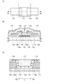
本実施の形態では、本発明の半導体装置の一態様について、図1(A)、(B)、(C)を用いて説明する。
本実施の形態では、実施の形態1に示す半導体装置の作製方法について、図1(B)を用いて以下説明する。また、実施の形態1で説明した機能と同様の機能を有する部分については、同様の符号を付し、その詳細な説明は省略する。
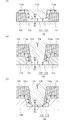
本実施の形態では、実施の形態1に示す半導体装置の変形例について、図2及び図3を用いて説明する。
従って、酸化物半導体層112のチャネル形成領域と、n型領域112aで、結晶部の結晶方向を異なる構造とすることができる。
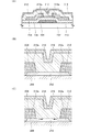
本実施の形態では、実施の形態1、及び実施の形態3に示す半導体装置の変形例について、図4及び図5を用いて説明を行う。また、実施の形態1、及び実施の形態3で説明した機能と同様の機能を有する部分については、同様の符号を付し、その詳細な説明は省略する。
本実施の形態では、本発明の一態様の半導体装置を用いた表示装置について、図6を用いて説明を行う。
104 ゲート電極層
106 ゲート絶縁層
106a 第1の被形成面
106b 第2の被形成面
106c 第3の被形成面
108 ソース電極層
108a 第2の被形成面
110 ドレイン電極層
110a 第3の被形成面
112 酸化物半導体層
112a n型領域
113 酸化物層
114 第3の絶縁層
116 第4の絶縁層
118a 第1の絶縁層
118a1 第2の被形成面
118b 第2の絶縁層
118b1 第3の被形成面
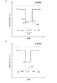
120 トラップ準位
122,124,126,128,130,132 交差部
133 混合層
152 酸化物積層
202 基板
204 ゲート電極層
206 ゲート絶縁層
208 ソース電極層
210 ドレイン電極層
212 酸化物半導体層
212a n型領域
214 第3の絶縁層
216 第4の絶縁層
302 第1の基板
304 ゲート電極層
306 ゲート絶縁層
308 ソース電極層
310 ドレイン電極層
312 酸化物半導体層
314 第3の絶縁層
316 第4の絶縁層
318 平坦化絶縁層
320 第5の絶縁層
322 画素電極層
324 第1の配向膜
352 第2の基板
354 有色層
356 遮光層
358 有機絶縁層
360 対向電極層
362 配向膜
364 液晶層
374 画素部
376 ゲートドライバ回路部
378 ソースドライバ回路部
Claims (11)
- ゲート電極層と、
前記ゲート電極層上のゲート絶縁層と、
前記ゲート絶縁層上の絶縁層と、
前記ゲート絶縁層と前記絶縁層によって形成された凹部と、
前記凹部に沿って形成された結晶部を含む酸化物半導体層と、
前記絶縁層、及び前記酸化物半導体層上のソース電極層、及びドレイン電極層と、を有し、
前記酸化物半導体層は、チャネル形成領域と、前記ソース電極層及び前記ドレイン電極層と接するn型領域と、を有し、
前記チャネル形成領域と、前記n型領域で、前記結晶部の結晶方向が異なり、
前記絶縁層は、酸化シリコン膜、酸化窒化シリコン膜、窒化酸化シリコン膜、窒化シリコン膜、酸化アルミニウム膜、窒化シリコン膜、及び窒化酸化シリコン膜の群から選択された一からなる単層、または前記群から選択された複数の膜からなる積層である
ことを特徴とする半導体装置。 - ゲート電極層と、
前記ゲート電極層上のゲート絶縁層と、
前記ゲート絶縁層上の第1の絶縁層及び第2の絶縁層と、
前記ゲート絶縁層、前記第1の絶縁層、及び前記第2の絶縁層上の結晶部を含む酸化物半導体層と、
前記第1の絶縁層、及び前記酸化物半導体層上のソース電極層と、
前記第2の絶縁層、及び前記酸化物半導体層上のドレイン電極層と、を有し、
前記酸化物半導体層は、チャネル形成領域と、前記ソース電極層及び前記ドレイン電極層と接するn型領域と、を有し、
前記チャネル形成領域は、前記ゲート絶縁層と接する前記酸化物半導体層に位置し、
前記ゲート絶縁層が前記酸化物半導体層に接する面は、前記第1の絶縁層が前記酸化物半導体層に接する面、及び前記第2の絶縁層が前記酸化物半導体層に接する面それぞれと交差し、
前記第1の絶縁層及び前記第2の絶縁層それぞれは、酸化シリコン膜、酸化窒化シリコン膜、窒化酸化シリコン膜、窒化シリコン膜、酸化アルミニウム膜、窒化シリコン膜、及び窒化酸化シリコン膜の群から選択された一からなる単層、または前記群から選択された複数の膜からなる積層である
ことを特徴とする半導体装置。 - ゲート電極層と、
前記ゲート電極層上の凹部を有するゲート絶縁層と、
前記凹部に沿って形成された結晶部を含む酸化物半導体層と、
前記ゲート絶縁層、及び前記酸化物半導体層上のソース電極層、及びドレイン電極層と、を有し、
前記酸化物半導体層は、チャネル形成領域と、前記ソース電極層及び前記ドレイン電極層と接するn型領域と、を有し、
前記チャネル形成領域と、前記n型領域で、前記結晶部の結晶方向が異なり、
前記ゲート絶縁層は、前記ゲート電極層の上面全てに接する
ことを特徴とする半導体装置。 - ゲート電極層と、
前記ゲート電極層上の第1の被形成面、第2の被形成面、及び第3の被形成面を有するゲート絶縁層と、
前記第1の被形成面、前記第2の被形成面、及び前記第3の被形成面上の結晶部を含む酸化物半導体層と、
前記第2の被形成面上の前記酸化物半導体層に接するソース電極層と、
前記第3の被形成面上の前記酸化物半導体層に接するドレイン電極層と、を有し、
前記酸化物半導体層は、チャネル形成領域と、前記ソース電極層及び前記ドレイン電極層と接するn型領域と、を有し、
前記チャネル形成領域は、前記第1の被形成面上の前記酸化物半導体層に位置し、
前記第1の被形成面は、前記第2の被形成面及び前記第3の被形成面それぞれと交差し、
前記ゲート絶縁層は、前記ゲート電極層の上面全てに接する
ことを特徴とする半導体装置。 - 請求項1乃至請求項4のいずれか一において、
前記酸化物半導体層は、
少なくともインジウム(In)、亜鉛(Zn)及びM(Al、Ga、Ge、Y、Zr、Sn、La、CeまたはHfの金属)を含むIn−M−Zn酸化物で表記される酸化物である
ことを特徴とする半導体装置。 - 請求項1乃至請求項5のいずれか一において、
前記酸化物半導体層は、
In−Ga−Zn酸化物で表記される酸化物である
ことを特徴とする半導体装置。 - 請求項1乃至請求項6のいずれか一において、
前記結晶部は、c軸が前記酸化物半導体層の被形成面の法線ベクトルに平行な方向に揃う
ことを特徴とする半導体装置。 - 請求項1または2において、
前記酸化物半導体層は、CAAC−OSを有する
ことを特徴とする半導体装置。 - 請求項1乃至請求項8のいずれか一に記載する半導体装置を有する表示装置。
- ゲート電極層上にゲート絶縁層を形成し、
前記ゲート絶縁層上に第1の絶縁層及び第2の絶縁層を形成し、
前記ゲート絶縁層、前記第1の絶縁層、及び前記第2の絶縁層上に結晶部を含む酸化物半導体層を形成し、
前記第1の絶縁層、及び前記酸化物半導体層上にソース電極層を形成し、
前記第2の絶縁層、及び前記酸化物半導体層上にドレイン電極層を形成する半導体装置の作製方法であり、
前記酸化物半導体層は、チャネル形成領域と、前記ソース電極層及び前記ドレイン電極層と接するn型領域と、を有し、
前記チャネル形成領域は、前記ゲート絶縁層と接する前記酸化物半導体層に位置し、
前記ゲート絶縁層が前記酸化物半導体層に接する面は、前記第1の絶縁層が前記酸化物半導体層に接する面、及び前記第2の絶縁層が前記酸化物半導体層に接する面それぞれと交差し、
前記第1の絶縁層及び前記第2の絶縁層それぞれは、酸化シリコン膜、酸化窒化シリコン膜、窒化酸化シリコン膜、窒化シリコン膜、酸化アルミニウム膜、窒化シリコン膜、及び窒化酸化シリコン膜の群から選択された一からなる単層、または前記群から選択された複数の膜からなる積層である
ことを特徴とする半導体装置の作製方法。 - ゲート電極層上に、前記ゲート電極層の上面全てに接し、且つ第1の被形成面、第2の被形成面、及び第3の被形成面を有するゲート絶縁層を形成し、
前記第1の被形成面、前記第2の被形成面、及び前記第3の被形成面上に結晶部を含む酸化物半導体層を形成し、
前記第2の被形成面上の前記酸化物半導体層に接するソース電極層を形成し、
前記第3の被形成面上の前記酸化物半導体層に接するドレイン電極層を形成する半導体装置の作製方法であり、
前記酸化物半導体層は、チャネル形成領域と、前記ソース電極層及び前記ドレイン電極層と接するn型領域と、を有し、
前記チャネル形成領域は、前記第1の被形成面上の前記酸化物半導体層に位置し、
前記第1の被形成面は、前記第2の被形成面及び前記第3の被形成面それぞれと交差する
ことを特徴とする半導体装置の作製方法。
Priority Applications (2)
| Application Number | Priority Date | Filing Date | Title |
|---|---|---|---|
| JP2013083132A JP6224338B2 (ja) | 2013-04-11 | 2013-04-11 | 半導体装置、表示装置及び半導体装置の作製方法 |
| US14/246,493 US9748399B2 (en) | 2013-04-11 | 2014-04-07 | Semiconductor device and display device comprising an oxide semiconductor channel region having a different crystal orientation than source/drain regions |
Applications Claiming Priority (1)
| Application Number | Priority Date | Filing Date | Title |
|---|---|---|---|
| JP2013083132A JP6224338B2 (ja) | 2013-04-11 | 2013-04-11 | 半導体装置、表示装置及び半導体装置の作製方法 |
Publications (2)
| Publication Number | Publication Date |
|---|---|
| JP2014207286A JP2014207286A (ja) | 2014-10-30 |
| JP6224338B2 true JP6224338B2 (ja) | 2017-11-01 |
Family
ID=51686185
Family Applications (1)
| Application Number | Title | Priority Date | Filing Date |
|---|---|---|---|
| JP2013083132A Active JP6224338B2 (ja) | 2013-04-11 | 2013-04-11 | 半導体装置、表示装置及び半導体装置の作製方法 |
Country Status (2)
| Country | Link |
|---|---|
| US (1) | US9748399B2 (ja) |
| JP (1) | JP6224338B2 (ja) |
Families Citing this family (4)
| Publication number | Priority date | Publication date | Assignee | Title |
|---|---|---|---|---|
| US9806200B2 (en) * | 2015-03-27 | 2017-10-31 | Semiconductor Energy Laboratory Co., Ltd. | Semiconductor device |
| US10976627B2 (en) * | 2015-12-01 | 2021-04-13 | Sharp Kabushiki Kaisha | Active matrix substrate and liquid crystal display panel comprising same |
| US20180356660A1 (en) * | 2015-12-09 | 2018-12-13 | Sharp Kabushiki Kaisha | Active matrix substrate and liquid crystal display panel provided with same |
| WO2017150275A1 (ja) * | 2016-02-29 | 2017-09-08 | シャープ株式会社 | 薄膜トランジスタ |
Family Cites Families (115)
| Publication number | Priority date | Publication date | Assignee | Title |
|---|---|---|---|---|
| JPS60198861A (ja) | 1984-03-23 | 1985-10-08 | Fujitsu Ltd | 薄膜トランジスタ |
| JPH0244256B2 (ja) | 1987-01-28 | 1990-10-03 | Kagaku Gijutsucho Mukizaishitsu Kenkyushocho | Ingazn2o5deshimesarerurotsuhoshokeinosojokozoojusurukagobutsuoyobisonoseizoho |
| JPS63210023A (ja) | 1987-02-24 | 1988-08-31 | Natl Inst For Res In Inorg Mater | InGaZn↓4O↓7で示される六方晶系の層状構造を有する化合物およびその製造法 |
| JPH0244260B2 (ja) | 1987-02-24 | 1990-10-03 | Kagaku Gijutsucho Mukizaishitsu Kenkyushocho | Ingazn5o8deshimesarerurotsuhoshokeinosojokozoojusurukagobutsuoyobisonoseizoho |
| JPH0244258B2 (ja) | 1987-02-24 | 1990-10-03 | Kagaku Gijutsucho Mukizaishitsu Kenkyushocho | Ingazn3o6deshimesarerurotsuhoshokeinosojokozoojusurukagobutsuoyobisonoseizoho |
| JPH0244262B2 (ja) | 1987-02-27 | 1990-10-03 | Kagaku Gijutsucho Mukizaishitsu Kenkyushocho | Ingazn6o9deshimesarerurotsuhoshokeinosojokozoojusurukagobutsuoyobisonoseizoho |
| JPH0244263B2 (ja) | 1987-04-22 | 1990-10-03 | Kagaku Gijutsucho Mukizaishitsu Kenkyushocho | Ingazn7o10deshimesarerurotsuhoshokeinosojokozoojusurukagobutsuoyobisonoseizoho |
| JPH05251705A (ja) | 1992-03-04 | 1993-09-28 | Fuji Xerox Co Ltd | 薄膜トランジスタ |
| JP3479375B2 (ja) | 1995-03-27 | 2003-12-15 | 科学技術振興事業団 | 亜酸化銅等の金属酸化物半導体による薄膜トランジスタとpn接合を形成した金属酸化物半導体装置およびそれらの製造方法 |
| JPH11505377A (ja) | 1995-08-03 | 1999-05-18 | フィリップス エレクトロニクス ネムローゼ フェンノートシャップ | 半導体装置 |
| JP3625598B2 (ja) | 1995-12-30 | 2005-03-02 | 三星電子株式会社 | 液晶表示装置の製造方法 |
| JP4170454B2 (ja) | 1998-07-24 | 2008-10-22 | Hoya株式会社 | 透明導電性酸化物薄膜を有する物品及びその製造方法 |
| JP2000150861A (ja) | 1998-11-16 | 2000-05-30 | Tdk Corp | 酸化物薄膜 |
| JP3276930B2 (ja) | 1998-11-17 | 2002-04-22 | 科学技術振興事業団 | トランジスタ及び半導体装置 |
| TW460731B (en) | 1999-09-03 | 2001-10-21 | Ind Tech Res Inst | Electrode structure and production method of wide viewing angle LCD |
| JP4089858B2 (ja) | 2000-09-01 | 2008-05-28 | 国立大学法人東北大学 | 半導体デバイス |
| KR20020038482A (ko) | 2000-11-15 | 2002-05-23 | 모리시타 요이찌 | 박막 트랜지스터 어레이, 그 제조방법 및 그것을 이용한표시패널 |
| JP3997731B2 (ja) | 2001-03-19 | 2007-10-24 | 富士ゼロックス株式会社 | 基材上に結晶性半導体薄膜を形成する方法 |
| JP2002289859A (ja) | 2001-03-23 | 2002-10-04 | Minolta Co Ltd | 薄膜トランジスタ |
| JP3925839B2 (ja) | 2001-09-10 | 2007-06-06 | シャープ株式会社 | 半導体記憶装置およびその試験方法 |
| JP4090716B2 (ja) | 2001-09-10 | 2008-05-28 | 雅司 川崎 | 薄膜トランジスタおよびマトリクス表示装置 |
| JP4164562B2 (ja) | 2002-09-11 | 2008-10-15 | 独立行政法人科学技術振興機構 | ホモロガス薄膜を活性層として用いる透明薄膜電界効果型トランジスタ |
| EP1443130B1 (en) | 2001-11-05 | 2011-09-28 | Japan Science and Technology Agency | Natural superlattice homologous single crystal thin film, method for preparation thereof, and device using said single crystal thin film |
| JP4083486B2 (ja) | 2002-02-21 | 2008-04-30 | 独立行政法人科学技術振興機構 | LnCuO(S,Se,Te)単結晶薄膜の製造方法 |
| US7049190B2 (en) | 2002-03-15 | 2006-05-23 | Sanyo Electric Co., Ltd. | Method for forming ZnO film, method for forming ZnO semiconductor layer, method for fabricating semiconductor device, and semiconductor device |
| JP3933591B2 (ja) | 2002-03-26 | 2007-06-20 | 淳二 城戸 | 有機エレクトロルミネッセント素子 |
| US7339187B2 (en) | 2002-05-21 | 2008-03-04 | State Of Oregon Acting By And Through The Oregon State Board Of Higher Education On Behalf Of Oregon State University | Transistor structures |
| JP2004022625A (ja) | 2002-06-13 | 2004-01-22 | Murata Mfg Co Ltd | 半導体デバイス及び該半導体デバイスの製造方法 |
| US7105868B2 (en) | 2002-06-24 | 2006-09-12 | Cermet, Inc. | High-electron mobility transistor with zinc oxide |
| US7067843B2 (en) | 2002-10-11 | 2006-06-27 | E. I. Du Pont De Nemours And Company | Transparent oxide semiconductor thin film transistors |
| JP4166105B2 (ja) | 2003-03-06 | 2008-10-15 | シャープ株式会社 | 半導体装置およびその製造方法 |
| JP2004273732A (ja) | 2003-03-07 | 2004-09-30 | Sharp Corp | アクティブマトリクス基板およびその製造方法 |
| JP4108633B2 (ja) | 2003-06-20 | 2008-06-25 | シャープ株式会社 | 薄膜トランジスタおよびその製造方法ならびに電子デバイス |
| US7262463B2 (en) | 2003-07-25 | 2007-08-28 | Hewlett-Packard Development Company, L.P. | Transistor including a deposited channel region having a doped portion |
| US7282782B2 (en) | 2004-03-12 | 2007-10-16 | Hewlett-Packard Development Company, L.P. | Combined binary oxide semiconductor device |
| US7145174B2 (en) | 2004-03-12 | 2006-12-05 | Hewlett-Packard Development Company, Lp. | Semiconductor device |
| US7297977B2 (en) | 2004-03-12 | 2007-11-20 | Hewlett-Packard Development Company, L.P. | Semiconductor device |
| KR20070116889A (ko) | 2004-03-12 | 2007-12-11 | 도꾸리쯔교세이호징 가가꾸 기쥬쯔 신꼬 기꼬 | 아몰퍼스 산화물 박막의 기상성막방법 |
| US7211825B2 (en) | 2004-06-14 | 2007-05-01 | Yi-Chi Shih | Indium oxide-based thin film transistors and circuits |
| JP2006100760A (ja) | 2004-09-02 | 2006-04-13 | Casio Comput Co Ltd | 薄膜トランジスタおよびその製造方法 |
| US7285501B2 (en) | 2004-09-17 | 2007-10-23 | Hewlett-Packard Development Company, L.P. | Method of forming a solution processed device |
| US7298084B2 (en) | 2004-11-02 | 2007-11-20 | 3M Innovative Properties Company | Methods and displays utilizing integrated zinc oxide row and column drivers in conjunction with organic light emitting diodes |
| EP1810335B1 (en) | 2004-11-10 | 2020-05-27 | Canon Kabushiki Kaisha | Light-emitting device |
| AU2005302964B2 (en) | 2004-11-10 | 2010-11-04 | Canon Kabushiki Kaisha | Field effect transistor employing an amorphous oxide |
| US7791072B2 (en) | 2004-11-10 | 2010-09-07 | Canon Kabushiki Kaisha | Display |
| KR100939998B1 (ko) | 2004-11-10 | 2010-02-03 | 캐논 가부시끼가이샤 | 비정질 산화물 및 전계 효과 트랜지스터 |
| US7863611B2 (en) | 2004-11-10 | 2011-01-04 | Canon Kabushiki Kaisha | Integrated circuits utilizing amorphous oxides |
| US7453065B2 (en) | 2004-11-10 | 2008-11-18 | Canon Kabushiki Kaisha | Sensor and image pickup device |
| US7829444B2 (en) | 2004-11-10 | 2010-11-09 | Canon Kabushiki Kaisha | Field effect transistor manufacturing method |
| US7579224B2 (en) | 2005-01-21 | 2009-08-25 | Semiconductor Energy Laboratory Co., Ltd. | Method for manufacturing a thin film semiconductor device |
| TWI481024B (zh) | 2005-01-28 | 2015-04-11 | 半導體能源研究所股份有限公司 | 半導體裝置,電子裝置,和半導體裝置的製造方法 |
| TWI562380B (en) | 2005-01-28 | 2016-12-11 | Semiconductor Energy Lab Co Ltd | Semiconductor device, electronic device, and method of manufacturing semiconductor device |
| US7858451B2 (en) | 2005-02-03 | 2010-12-28 | Semiconductor Energy Laboratory Co., Ltd. | Electronic device, semiconductor device and manufacturing method thereof |
| US7948171B2 (en) | 2005-02-18 | 2011-05-24 | Semiconductor Energy Laboratory Co., Ltd. | Light emitting device |
| US20060197092A1 (en) | 2005-03-03 | 2006-09-07 | Randy Hoffman | System and method for forming conductive material on a substrate |
| US8681077B2 (en) | 2005-03-18 | 2014-03-25 | Semiconductor Energy Laboratory Co., Ltd. | Semiconductor device, and display device, driving method and electronic apparatus thereof |
| WO2006105077A2 (en) | 2005-03-28 | 2006-10-05 | Massachusetts Institute Of Technology | Low voltage thin film transistor with high-k dielectric material |
| US7645478B2 (en) | 2005-03-31 | 2010-01-12 | 3M Innovative Properties Company | Methods of making displays |
| US8300031B2 (en) | 2005-04-20 | 2012-10-30 | Semiconductor Energy Laboratory Co., Ltd. | Semiconductor device comprising transistor having gate and drain connected through a current-voltage conversion element |
| JP2006344849A (ja) | 2005-06-10 | 2006-12-21 | Casio Comput Co Ltd | 薄膜トランジスタ |
| US7691666B2 (en) | 2005-06-16 | 2010-04-06 | Eastman Kodak Company | Methods of making thin film transistors comprising zinc-oxide-based semiconductor materials and transistors made thereby |
| US7402506B2 (en) | 2005-06-16 | 2008-07-22 | Eastman Kodak Company | Methods of making thin film transistors comprising zinc-oxide-based semiconductor materials and transistors made thereby |
| US7507618B2 (en) | 2005-06-27 | 2009-03-24 | 3M Innovative Properties Company | Method for making electronic devices using metal oxide nanoparticles |
| KR100711890B1 (ko) | 2005-07-28 | 2007-04-25 | 삼성에스디아이 주식회사 | 유기 발광표시장치 및 그의 제조방법 |
| JP2007059128A (ja) | 2005-08-23 | 2007-03-08 | Canon Inc | 有機el表示装置およびその製造方法 |
| JP4850457B2 (ja) | 2005-09-06 | 2012-01-11 | キヤノン株式会社 | 薄膜トランジスタ及び薄膜ダイオード |
| JP5116225B2 (ja) | 2005-09-06 | 2013-01-09 | キヤノン株式会社 | 酸化物半導体デバイスの製造方法 |
| JP2007073705A (ja) | 2005-09-06 | 2007-03-22 | Canon Inc | 酸化物半導体チャネル薄膜トランジスタおよびその製造方法 |
| JP4280736B2 (ja) | 2005-09-06 | 2009-06-17 | キヤノン株式会社 | 半導体素子 |
| JP5064747B2 (ja) | 2005-09-29 | 2012-10-31 | 株式会社半導体エネルギー研究所 | 半導体装置、電気泳動表示装置、表示モジュール、電子機器、及び半導体装置の作製方法 |
| JP5078246B2 (ja) | 2005-09-29 | 2012-11-21 | 株式会社半導体エネルギー研究所 | 半導体装置、及び半導体装置の作製方法 |
| EP1998374A3 (en) | 2005-09-29 | 2012-01-18 | Semiconductor Energy Laboratory Co, Ltd. | Semiconductor device having oxide semiconductor layer and manufacturing method thereof |
| JP5037808B2 (ja) | 2005-10-20 | 2012-10-03 | キヤノン株式会社 | アモルファス酸化物を用いた電界効果型トランジスタ、及び該トランジスタを用いた表示装置 |
| KR101397571B1 (ko) | 2005-11-15 | 2014-05-22 | 가부시키가이샤 한도오따이 에네루기 켄큐쇼 | 반도체장치 및 그의 제조방법 |
| TWI292281B (en) | 2005-12-29 | 2008-01-01 | Ind Tech Res Inst | Pixel structure of active organic light emitting diode and method of fabricating the same |
| US7867636B2 (en) | 2006-01-11 | 2011-01-11 | Murata Manufacturing Co., Ltd. | Transparent conductive film and method for manufacturing the same |
| JP4977478B2 (ja) | 2006-01-21 | 2012-07-18 | 三星電子株式会社 | ZnOフィルム及びこれを用いたTFTの製造方法 |
| US7576394B2 (en) | 2006-02-02 | 2009-08-18 | Kochi Industrial Promotion Center | Thin film transistor including low resistance conductive thin films and manufacturing method thereof |
| US7977169B2 (en) | 2006-02-15 | 2011-07-12 | Kochi Industrial Promotion Center | Semiconductor device including active layer made of zinc oxide with controlled orientations and manufacturing method thereof |
| KR20070101595A (ko) | 2006-04-11 | 2007-10-17 | 삼성전자주식회사 | ZnO TFT |
| US20070252928A1 (en) | 2006-04-28 | 2007-11-01 | Toppan Printing Co., Ltd. | Structure, transmission type liquid crystal display, reflection type display and manufacturing method thereof |
| JP5028033B2 (ja) | 2006-06-13 | 2012-09-19 | キヤノン株式会社 | 酸化物半導体膜のドライエッチング方法 |
| JP4999400B2 (ja) | 2006-08-09 | 2012-08-15 | キヤノン株式会社 | 酸化物半導体膜のドライエッチング方法 |
| JP4609797B2 (ja) | 2006-08-09 | 2011-01-12 | Nec液晶テクノロジー株式会社 | 薄膜デバイス及びその製造方法 |
| JP4332545B2 (ja) | 2006-09-15 | 2009-09-16 | キヤノン株式会社 | 電界効果型トランジスタ及びその製造方法 |
| JP4274219B2 (ja) | 2006-09-27 | 2009-06-03 | セイコーエプソン株式会社 | 電子デバイス、有機エレクトロルミネッセンス装置、有機薄膜半導体装置 |
| JP5164357B2 (ja) | 2006-09-27 | 2013-03-21 | キヤノン株式会社 | 半導体装置及び半導体装置の製造方法 |
| US7622371B2 (en) | 2006-10-10 | 2009-11-24 | Hewlett-Packard Development Company, L.P. | Fused nanocrystal thin film semiconductor and method |
| US7772021B2 (en) | 2006-11-29 | 2010-08-10 | Samsung Electronics Co., Ltd. | Flat panel displays comprising a thin-film transistor having a semiconductive oxide in its channel and methods of fabricating the same for use in flat panel displays |
| JP2008140684A (ja) | 2006-12-04 | 2008-06-19 | Toppan Printing Co Ltd | カラーelディスプレイおよびその製造方法 |
| KR101303578B1 (ko) | 2007-01-05 | 2013-09-09 | 삼성전자주식회사 | 박막 식각 방법 |
| US8207063B2 (en) | 2007-01-26 | 2012-06-26 | Eastman Kodak Company | Process for atomic layer deposition |
| KR100851215B1 (ko) | 2007-03-14 | 2008-08-07 | 삼성에스디아이 주식회사 | 박막 트랜지스터 및 이를 이용한 유기 전계 발광표시장치 |
| US7795613B2 (en) | 2007-04-17 | 2010-09-14 | Toppan Printing Co., Ltd. | Structure with transistor |
| KR101325053B1 (ko) | 2007-04-18 | 2013-11-05 | 삼성디스플레이 주식회사 | 박막 트랜지스터 기판 및 이의 제조 방법 |
| KR20080094300A (ko) | 2007-04-19 | 2008-10-23 | 삼성전자주식회사 | 박막 트랜지스터 및 그 제조 방법과 박막 트랜지스터를포함하는 평판 디스플레이 |
| KR101334181B1 (ko) | 2007-04-20 | 2013-11-28 | 삼성전자주식회사 | 선택적으로 결정화된 채널층을 갖는 박막 트랜지스터 및 그제조 방법 |
| US8274078B2 (en) | 2007-04-25 | 2012-09-25 | Canon Kabushiki Kaisha | Metal oxynitride semiconductor containing zinc |
| KR101345376B1 (ko) | 2007-05-29 | 2013-12-24 | 삼성전자주식회사 | ZnO 계 박막 트랜지스터 및 그 제조방법 |
| JP5215158B2 (ja) | 2007-12-17 | 2013-06-19 | 富士フイルム株式会社 | 無機結晶性配向膜及びその製造方法、半導体デバイス |
| JP5644071B2 (ja) * | 2008-08-20 | 2014-12-24 | 株式会社リコー | 電界効果型トランジスタ、表示素子、画像表示装置及びシステム |
| JP4623179B2 (ja) | 2008-09-18 | 2011-02-02 | ソニー株式会社 | 薄膜トランジスタおよびその製造方法 |
| JP5451280B2 (ja) | 2008-10-09 | 2014-03-26 | キヤノン株式会社 | ウルツ鉱型結晶成長用基板およびその製造方法ならびに半導体装置 |
| CN101740631B (zh) * | 2008-11-07 | 2014-07-16 | 株式会社半导体能源研究所 | 半导体装置及该半导体装置的制造方法 |
| EP2544237B1 (en) | 2009-09-16 | 2017-05-03 | Semiconductor Energy Laboratory Co., Ltd. | Transistor and display device |
| KR20120071398A (ko) | 2009-09-16 | 2012-07-02 | 가부시키가이샤 한도오따이 에네루기 켄큐쇼 | 반도체 장치 및 그 제조 방법 |
| WO2011036999A1 (en) * | 2009-09-24 | 2011-03-31 | Semiconductor Energy Laboratory Co., Ltd. | Oxide semiconductor film and semiconductor device |
| JP4875135B2 (ja) * | 2009-11-18 | 2012-02-15 | 出光興産株式会社 | In−Ga−Zn−O系スパッタリングターゲット |
| WO2011065210A1 (en) * | 2009-11-28 | 2011-06-03 | Semiconductor Energy Laboratory Co., Ltd. | Stacked oxide material, semiconductor device, and method for manufacturing the semiconductor device |
| KR101977152B1 (ko) * | 2010-04-02 | 2019-05-10 | 가부시키가이샤 한도오따이 에네루기 켄큐쇼 | 반도체 장치 |
| US8685787B2 (en) * | 2010-08-25 | 2014-04-01 | Semiconductor Energy Laboratory Co., Ltd. | Manufacturing method of semiconductor device |
| US8957418B2 (en) | 2010-12-08 | 2015-02-17 | Sharp Kabushiki Kaisha | Semiconductor device and display apparatus |
| JP5404963B2 (ja) * | 2011-03-01 | 2014-02-05 | シャープ株式会社 | 薄膜トランジスタおよび表示装置 |
| KR20120124126A (ko) * | 2011-05-03 | 2012-11-13 | 삼성디스플레이 주식회사 | 산화물 반도체 소자, 산화물 반도체 소자의 제조 방법 및 산화물 반도체소자를 포함하는 표시 장치 |
| KR101851565B1 (ko) * | 2011-08-17 | 2018-04-25 | 삼성전자주식회사 | 트랜지스터와 그 제조방법 및 트랜지스터를 포함하는 전자소자 |
-
2013
- 2013-04-11 JP JP2013083132A patent/JP6224338B2/ja active Active
-
2014
- 2014-04-07 US US14/246,493 patent/US9748399B2/en active Active
Also Published As
| Publication number | Publication date |
|---|---|
| US20140306220A1 (en) | 2014-10-16 |
| JP2014207286A (ja) | 2014-10-30 |
| US9748399B2 (en) | 2017-08-29 |
Similar Documents
| Publication | Publication Date | Title |
|---|---|---|
| KR102582722B1 (ko) | 반도체 장치 | |
| JP7329575B2 (ja) | 半導体装置 | |
| JP6595563B2 (ja) | トランジスタ | |
| TWI716941B (zh) | 顯示裝置 | |
| TWI802017B (zh) | 半導體裝置 | |
| TWI679480B (zh) | 顯示裝置及具有該顯示裝置的電子裝置 | |
| JP6317059B2 (ja) | 半導体装置及び表示装置 | |
| JP6198434B2 (ja) | 表示装置及び電子機器 | |
| JP6224338B2 (ja) | 半導体装置、表示装置及び半導体装置の作製方法 | |
| US9312278B2 (en) | Display device and electronic device | |
| WO2013179837A1 (ja) | 半導体装置およびその製造方法 |
Legal Events
| Date | Code | Title | Description |
|---|---|---|---|
| A621 | Written request for application examination |
Free format text: JAPANESE INTERMEDIATE CODE: A621 Effective date: 20160325 |
|
| A977 | Report on retrieval |
Free format text: JAPANESE INTERMEDIATE CODE: A971007 Effective date: 20170131 |
|
| A131 | Notification of reasons for refusal |
Free format text: JAPANESE INTERMEDIATE CODE: A131 Effective date: 20170228 |
|
| A521 | Request for written amendment filed |
Free format text: JAPANESE INTERMEDIATE CODE: A523 Effective date: 20170418 |
|
| TRDD | Decision of grant or rejection written | ||
| A01 | Written decision to grant a patent or to grant a registration (utility model) |
Free format text: JAPANESE INTERMEDIATE CODE: A01 Effective date: 20170926 |
|
| A61 | First payment of annual fees (during grant procedure) |
Free format text: JAPANESE INTERMEDIATE CODE: A61 Effective date: 20171005 |
|
| R150 | Certificate of patent or registration of utility model |
Ref document number: 6224338 Country of ref document: JP Free format text: JAPANESE INTERMEDIATE CODE: R150 |
|
| R250 | Receipt of annual fees |
Free format text: JAPANESE INTERMEDIATE CODE: R250 |
|
| R250 | Receipt of annual fees |
Free format text: JAPANESE INTERMEDIATE CODE: R250 |
|
| R250 | Receipt of annual fees |
Free format text: JAPANESE INTERMEDIATE CODE: R250 |
|
| R250 | Receipt of annual fees |
Free format text: JAPANESE INTERMEDIATE CODE: R250 |
|
| R250 | Receipt of annual fees |
Free format text: JAPANESE INTERMEDIATE CODE: R250 |
|
| R250 | Receipt of annual fees |
Free format text: JAPANESE INTERMEDIATE CODE: R250 |