JP5950488B1 - 半導体モジュール - Google Patents
半導体モジュール Download PDFInfo
- Publication number
- JP5950488B1 JP5950488B1 JP2015522811A JP2015522811A JP5950488B1 JP 5950488 B1 JP5950488 B1 JP 5950488B1 JP 2015522811 A JP2015522811 A JP 2015522811A JP 2015522811 A JP2015522811 A JP 2015522811A JP 5950488 B1 JP5950488 B1 JP 5950488B1
- Authority
- JP
- Japan
- Prior art keywords
- circuit board
- semiconductor element
- semiconductor
- rectangular parallelepiped
- connector
- Prior art date
- Legal status (The legal status is an assumption and is not a legal conclusion. Google has not performed a legal analysis and makes no representation as to the accuracy of the status listed.)
- Active
Links
Images
Classifications
-
- H—ELECTRICITY
- H10—SEMICONDUCTOR DEVICES; ELECTRIC SOLID-STATE DEVICES NOT OTHERWISE PROVIDED FOR
- H10W—GENERIC PACKAGES, INTERCONNECTIONS, CONNECTORS OR OTHER CONSTRUCTIONAL DETAILS OF DEVICES COVERED BY CLASS H10
- H10W40/00—Arrangements for thermal protection or thermal control
- H10W40/20—Arrangements for cooling
- H10W40/22—Arrangements for cooling characterised by their shape, e.g. having conical or cylindrical projections
- H10W40/226—Arrangements for cooling characterised by their shape, e.g. having conical or cylindrical projections characterised by projecting parts, e.g. fins to increase surface area
- H10W40/228—Arrangements for cooling characterised by their shape, e.g. having conical or cylindrical projections characterised by projecting parts, e.g. fins to increase surface area the projecting parts being wire-shaped or pin-shaped
-
- H—ELECTRICITY
- H10—SEMICONDUCTOR DEVICES; ELECTRIC SOLID-STATE DEVICES NOT OTHERWISE PROVIDED FOR
- H10W—GENERIC PACKAGES, INTERCONNECTIONS, CONNECTORS OR OTHER CONSTRUCTIONAL DETAILS OF DEVICES COVERED BY CLASS H10
- H10W40/00—Arrangements for thermal protection or thermal control
- H10W40/20—Arrangements for cooling
- H10W40/25—Arrangements for cooling characterised by their materials
- H10W40/255—Arrangements for cooling characterised by their materials having a laminate or multilayered structure, e.g. direct bond copper [DBC] ceramic substrates
-
- H—ELECTRICITY
- H10—SEMICONDUCTOR DEVICES; ELECTRIC SOLID-STATE DEVICES NOT OTHERWISE PROVIDED FOR
- H10W—GENERIC PACKAGES, INTERCONNECTIONS, CONNECTORS OR OTHER CONSTRUCTIONAL DETAILS OF DEVICES COVERED BY CLASS H10
- H10W70/00—Package substrates; Interposers; Redistribution layers [RDL]
- H10W70/20—Conductive package substrates serving as an interconnection, e.g. metal plates
-
- H—ELECTRICITY
- H10—SEMICONDUCTOR DEVICES; ELECTRIC SOLID-STATE DEVICES NOT OTHERWISE PROVIDED FOR
- H10W—GENERIC PACKAGES, INTERCONNECTIONS, CONNECTORS OR OTHER CONSTRUCTIONAL DETAILS OF DEVICES COVERED BY CLASS H10
- H10W70/00—Package substrates; Interposers; Redistribution layers [RDL]
- H10W70/40—Leadframes
- H10W70/464—Additional interconnections in combination with leadframes
- H10W70/468—Circuit boards
-
- H—ELECTRICITY
- H10—SEMICONDUCTOR DEVICES; ELECTRIC SOLID-STATE DEVICES NOT OTHERWISE PROVIDED FOR
- H10W—GENERIC PACKAGES, INTERCONNECTIONS, CONNECTORS OR OTHER CONSTRUCTIONAL DETAILS OF DEVICES COVERED BY CLASS H10
- H10W72/00—Interconnections or connectors in packages
- H10W72/60—Strap connectors, e.g. thick copper clips for grounding of power devices
-
- H—ELECTRICITY
- H10—SEMICONDUCTOR DEVICES; ELECTRIC SOLID-STATE DEVICES NOT OTHERWISE PROVIDED FOR
- H10W—GENERIC PACKAGES, INTERCONNECTIONS, CONNECTORS OR OTHER CONSTRUCTIONAL DETAILS OF DEVICES COVERED BY CLASS H10
- H10W90/00—Package configurations
-
- H—ELECTRICITY
- H10—SEMICONDUCTOR DEVICES; ELECTRIC SOLID-STATE DEVICES NOT OTHERWISE PROVIDED FOR
- H10W—GENERIC PACKAGES, INTERCONNECTIONS, CONNECTORS OR OTHER CONSTRUCTIONAL DETAILS OF DEVICES COVERED BY CLASS H10
- H10W90/00—Package configurations
- H10W90/401—Package configurations characterised by multiple insulating or insulated package substrates, interposers or RDLs
-
- H—ELECTRICITY
- H10—SEMICONDUCTOR DEVICES; ELECTRIC SOLID-STATE DEVICES NOT OTHERWISE PROVIDED FOR
- H10W—GENERIC PACKAGES, INTERCONNECTIONS, CONNECTORS OR OTHER CONSTRUCTIONAL DETAILS OF DEVICES COVERED BY CLASS H10
- H10W72/00—Interconnections or connectors in packages
- H10W72/071—Connecting or disconnecting
- H10W72/073—Connecting or disconnecting of die-attach connectors
- H10W72/07331—Connecting techniques
- H10W72/07336—Soldering or alloying
-
- H—ELECTRICITY
- H10—SEMICONDUCTOR DEVICES; ELECTRIC SOLID-STATE DEVICES NOT OTHERWISE PROVIDED FOR
- H10W—GENERIC PACKAGES, INTERCONNECTIONS, CONNECTORS OR OTHER CONSTRUCTIONAL DETAILS OF DEVICES COVERED BY CLASS H10
- H10W72/00—Interconnections or connectors in packages
- H10W72/071—Connecting or disconnecting
- H10W72/073—Connecting or disconnecting of die-attach connectors
- H10W72/07331—Connecting techniques
- H10W72/07337—Connecting techniques using a polymer adhesive, e.g. an adhesive based on silicone or epoxy
-
- H—ELECTRICITY
- H10—SEMICONDUCTOR DEVICES; ELECTRIC SOLID-STATE DEVICES NOT OTHERWISE PROVIDED FOR
- H10W—GENERIC PACKAGES, INTERCONNECTIONS, CONNECTORS OR OTHER CONSTRUCTIONAL DETAILS OF DEVICES COVERED BY CLASS H10
- H10W72/00—Interconnections or connectors in packages
- H10W72/071—Connecting or disconnecting
- H10W72/076—Connecting or disconnecting of strap connectors
- H10W72/07631—Techniques
- H10W72/07636—Soldering or alloying
-
- H—ELECTRICITY
- H10—SEMICONDUCTOR DEVICES; ELECTRIC SOLID-STATE DEVICES NOT OTHERWISE PROVIDED FOR
- H10W—GENERIC PACKAGES, INTERCONNECTIONS, CONNECTORS OR OTHER CONSTRUCTIONAL DETAILS OF DEVICES COVERED BY CLASS H10
- H10W72/00—Interconnections or connectors in packages
- H10W72/071—Connecting or disconnecting
- H10W72/076—Connecting or disconnecting of strap connectors
- H10W72/07631—Techniques
- H10W72/07637—Techniques using a polymer adhesive, e.g. an adhesive based on silicone or epoxy
-
- H—ELECTRICITY
- H10—SEMICONDUCTOR DEVICES; ELECTRIC SOLID-STATE DEVICES NOT OTHERWISE PROVIDED FOR
- H10W—GENERIC PACKAGES, INTERCONNECTIONS, CONNECTORS OR OTHER CONSTRUCTIONAL DETAILS OF DEVICES COVERED BY CLASS H10
- H10W72/00—Interconnections or connectors in packages
- H10W72/60—Strap connectors, e.g. thick copper clips for grounding of power devices
- H10W72/651—Materials of strap connectors
- H10W72/652—Materials of strap connectors comprising metals or metalloids, e.g. silver
-
- H—ELECTRICITY
- H10—SEMICONDUCTOR DEVICES; ELECTRIC SOLID-STATE DEVICES NOT OTHERWISE PROVIDED FOR
- H10W—GENERIC PACKAGES, INTERCONNECTIONS, CONNECTORS OR OTHER CONSTRUCTIONAL DETAILS OF DEVICES COVERED BY CLASS H10
- H10W72/00—Interconnections or connectors in packages
- H10W72/60—Strap connectors, e.g. thick copper clips for grounding of power devices
- H10W72/651—Materials of strap connectors
- H10W72/655—Materials of strap connectors of outermost layers of multilayered strap connectors, e.g. material of a coating
-
- H—ELECTRICITY
- H10—SEMICONDUCTOR DEVICES; ELECTRIC SOLID-STATE DEVICES NOT OTHERWISE PROVIDED FOR
- H10W—GENERIC PACKAGES, INTERCONNECTIONS, CONNECTORS OR OTHER CONSTRUCTIONAL DETAILS OF DEVICES COVERED BY CLASS H10
- H10W90/00—Package configurations
- H10W90/20—Configurations of stacked chips
- H10W90/22—Configurations of stacked chips the stacked chips being on both top and bottom sides of a package substrate, interposer or RDL
-
- H—ELECTRICITY
- H10—SEMICONDUCTOR DEVICES; ELECTRIC SOLID-STATE DEVICES NOT OTHERWISE PROVIDED FOR
- H10W—GENERIC PACKAGES, INTERCONNECTIONS, CONNECTORS OR OTHER CONSTRUCTIONAL DETAILS OF DEVICES COVERED BY CLASS H10
- H10W90/00—Package configurations
- H10W90/20—Configurations of stacked chips
- H10W90/24—Configurations of stacked chips at least one of the stacked chips being laterally offset from a neighbouring stacked chip, e.g. chip stacks having a staircase shape
-
- H—ELECTRICITY
- H10—SEMICONDUCTOR DEVICES; ELECTRIC SOLID-STATE DEVICES NOT OTHERWISE PROVIDED FOR
- H10W—GENERIC PACKAGES, INTERCONNECTIONS, CONNECTORS OR OTHER CONSTRUCTIONAL DETAILS OF DEVICES COVERED BY CLASS H10
- H10W90/00—Package configurations
- H10W90/20—Configurations of stacked chips
- H10W90/288—Configurations of stacked chips characterised by arrangements for thermal management of the stacked chips
-
- H—ELECTRICITY
- H10—SEMICONDUCTOR DEVICES; ELECTRIC SOLID-STATE DEVICES NOT OTHERWISE PROVIDED FOR
- H10W—GENERIC PACKAGES, INTERCONNECTIONS, CONNECTORS OR OTHER CONSTRUCTIONAL DETAILS OF DEVICES COVERED BY CLASS H10
- H10W90/00—Package configurations
- H10W90/701—Package configurations characterised by the relative positions of pads or connectors relative to package parts
- H10W90/731—Package configurations characterised by the relative positions of pads or connectors relative to package parts of die-attach connectors
- H10W90/732—Package configurations characterised by the relative positions of pads or connectors relative to package parts of die-attach connectors between stacked chips
-
- H—ELECTRICITY
- H10—SEMICONDUCTOR DEVICES; ELECTRIC SOLID-STATE DEVICES NOT OTHERWISE PROVIDED FOR
- H10W—GENERIC PACKAGES, INTERCONNECTIONS, CONNECTORS OR OTHER CONSTRUCTIONAL DETAILS OF DEVICES COVERED BY CLASS H10
- H10W90/00—Package configurations
- H10W90/701—Package configurations characterised by the relative positions of pads or connectors relative to package parts
- H10W90/751—Package configurations characterised by the relative positions of pads or connectors relative to package parts of bond wires
- H10W90/752—Package configurations characterised by the relative positions of pads or connectors relative to package parts of bond wires between stacked chips
Landscapes
- Combinations Of Printed Boards (AREA)
- Cooling Or The Like Of Semiconductors Or Solid State Devices (AREA)
- Chemical & Material Sciences (AREA)
- Engineering & Computer Science (AREA)
- Ceramic Engineering (AREA)
Abstract
Description
したがって、本発明によれば、放熱性の高い半導体モジュールを提供することができる。
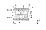
以下、本発明の第一の実施形態による半導体モジュールについて、図1A、図1Bおよび図2に基づいて説明する。
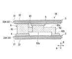
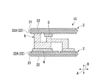
図1Aおよび図1Bに示すように、第一の実施形態による半導体モジュール1Aは、第一の回路基板2と、第一の回路基板2に対向配置された第二の回路基板3と、第一の回路基板2に接合された第一の半導体素子4と、第二の回路基板3に接合された第二の半導体素子5と、第一の半導体素子4および第二の半導体素子5を相互に電気接続する接続子6と、を備えている。
具体的には、第一の半導体素子4の一方の主面が、はんだ等の導電性接着剤(不図示)によって第一の回路基板2の第一の導電層22Aに接合され、第二の半導体素子5の一方の主面が、はんだ等の導電性接着剤(不図示)によって第二の回路基板3の第一の導電層32Aに接合されている。これにより、第一の半導体素子4が第一の回路基板2の第一の導電層22Aに電気接続され、第二の半導体素子5が第二の回路基板3の第一の導電層32Aに電気接続されている。
上記のように接合された第一の半導体素子4および第二の半導体素子5は、第二の回路基板3と対向する第一の回路基板2の対向面に直交する方向(図1A)において矢印Aの方向、以下、回路基板直交方向Aとする)から見て、互いに重畳しない位置に配置されている。
ここで、回路基板直交方向Aに直交する方向で、第一の半導体素子4および第二の半導体素子5が配列されている方向(図1Aにおいて矢印Bの方向)を第一の回路基板面方向Bとし、回路基板直交方向Aおよび第一の回路基板面方向Bに直交する方向(図1Bにおいて矢印Cの方向)を第二の回路基板面方向Cとして以下説明する。
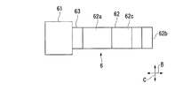
本実施形態の接続子6は、第一の半導体素子4と接合されている第一の素子接合部61と、第二の半導体素子5と接合されている第二の素子接合部62と、第一の素子接合部61と第二の素子接合部62とを接続する接続部63と、を有している。これらは、第一の素子接合部61、接続部63、第二の素子接合部62の順に第一の回路基板面方向Bの一方側から他方側に配列され、一体に形成されている。
接続子6の第一の素子接合部61および第二の半導体素子5は、ともに第二の回路基板3の第一の導電層32Aに接合されているが、第二の回路基板3の第一の導電層32Aにおいて、接続子6の第一の素子接合部61が接合される領域と、第二の半導体素子5が接合される領域とは、電気的に独立している。
第二の素子接合部62は、第二の半導体素子5とは回路基板直交方向Aに重畳し、第一の半導体素子4とは重畳しないように配置されている。
第二の直方体部62bのうち、第一の回路基板2側の端面は、はんだ等の導電性接着剤(不図示)によって第一の回路基板2の第一の導電層22Aに接合され、第二の回路基板3側の端面は、第二の回路基板3と離間している。
連結部62cは、接合第一の回路基板2、第二の回路基板3、第一の半導体素子4、および第二の半導体素子5に接合されていない。
接続子6の第二の素子接合部62および第一の半導体素子4は、ともに第一の回路基板2の第一の導電層22Aに接合されているが、第一の回路基板2の第一の導電層22Aにおいて、接続子6の第二の素子接合部62が接合される領域と、第一の半導体素子4が接合される領域とは、電気的に独立している。
なお、接続子6は、外部接続リード(不図示)に接合されていてもよい。例えば、図2に示すように、接続子6に外部接続リードと接合される外部接続部64が設けられていてもよい。図2に示す外部接続部64は、第一の素子接合部61から第一の回路基板面方向Bの接続部63と離間する方向に延びる形状に形成されている。
そして、第一の回路基板2および第二の回路基板3に伝わった第一の半導体素子4および第二の半導体素子5の熱は、半導体モジュール1Aの外部に放出することが可能である。例えば、第一の回路基板2や第二の回路基板3において第一の導電層22A,32Aと反対側に位置する他方の導電層22,32にヒートシンクを接触させることで、上記した熱を半導体モジュール1Aの外部に効率よく放出することができる。
第一の実施形態による半導体モジュール1Aでは、第一の半導体素子4と第二の半導体素子5とが回路基板直交方向Aに互いに重畳しない位置に配置されていて、接続子6が第二の半導体素子5を介さずに第一の半導体素子4と第二の回路基板3との間に挟み込まれた第一の素子接合部61を有する。これにより、第一の半導体素子4の熱を第二の半導体素子5を介さずに直接第二の回路基板3に伝えることができる。
また、接続子6が第一の半導体素子4を介さずに第二の半導体素子5と第一の回路基板2との間に挟み込まれた第二の素子接合部62を有することにより、第二の半導体素子5の熱を第一の半導体素子4を介さずに直接第一の回路基板2に伝えることができる。
このため、第一の半導体素子4および第二の半導体素子5の熱を、第一の回路基板2と第二の回路基板3との双方から効率よく放熱させることができる。
以上のことから、放熱性の高い半導体モジュール1Aを提供することができる。
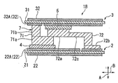
次に、第二の実施形態について、添付図面に基づいて説明するが、上述の第一の実施形態と同一又は同様な部材、部分には同一の符号を用いて説明を省略し、第一の実施形態と異なる構成について説明する。
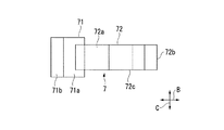
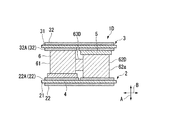
第二の直方体部71bのうち、第二の回路基板3側の端面は、はんだ等の導電性接着剤(不図示)によって第二の回路基板3の第一の導電層32Aに接合され、第一の回路基板2側の端面は、第一の直方体部71aに接合されている。
接続子7の第一の素子接合部71および第二の半導体素子5は、ともに第二の回路基板3の第一の導電層32Aに接合されているが、第二の回路基板3の第一の導電層32Aにおいて、接続子7の第一の素子接合部71が接合される領域と、第二の半導体素子5が接合される領域とは、電気的に独立している。
第二の直方体部72bのうち、第一の回路基板2側の端面は、はんだ等の導電性接着剤(不図示)によって第一の回路基板2の第一の導電層22Aに接合され、第二の回路基板3側の端面は、第二の回路基板3と離間している。
連結部72cは、第一の回路基板2、第二の回路基板3、第一の半導体素子4、および第二の半導体素子5に接合されていない。
接続子7の第二の素子接合部72および第一の半導体素子4は、ともに第一の回路基板2の第一の導電層22Aに接合されているが、第一の回路基板2の第一の導電層22Aにおいて、接続子7の第二の素子接合部72が接合される領域と、第一の半導体素子4が接合される領域とは、電気的に独立している。
そして、第一の回路基板2および第二の回路基板3に伝わった第一の半導体素子4および第二の半導体素子5の熱は、半導体モジュール1Bの外部に放出することが可能である。
また、本実施形態の半導体モジュール1Bによれば、第一の半導体素子4の一部と第二の半導体素子5の一部とが、回路基板直交方向Aに重畳するように配置されていることにより、第一の実施形態の半導体モジュール1Aと比較して、回路基板直交方向Aから見た大きさを小さくすることができる。すなわち、半導体モジュール1Bの小型化を図ることができる。
例えば、上記の実施形態では、第一の回路基板2および第二の回路基板3の導電層は、セラミック板21,31の両主面に設けられているが、セラミック板21,31の一方の主面のみに設けられてもよい。
また、第一の回路基板2と第二の回路基板3との間には、例えば第一の半導体素子4、第二の半導体素子5および接続子6,7を封止する封止樹脂が設けられてもよい。
このような場合にも、第二の半導体素子5において発生した熱を、第二の回路基板3だけではく、接続子6の第二の素子接合部62Dを介して第一の回路基板2にも伝えることができる。
このような場合にも、第二の半導体素子5において発生した熱を、第二の回路基板3だけではく、接続子7の第二の素子接合部72Eを介して第一の回路基板2にも伝えることができる。
2 第一の回路基板
3 第二の回路基板
4 第一の半導体素子
5 第二の半導体素子
6,7,8 接続子
A 回路基板直交方向
Claims (5)
- 熱伝導性を有する第一の回路基板と、
前記第一の回路基板と対向配置された熱伝導性を有する第二の回路基板と、
前記第二の回路基板と対向する前記第一の回路基板の対向面に接合された第一の半導体素子と、
前記第一の回路基板と対向する前記第二の回路基板の対向面に接合された第二の半導体素子と、
熱伝導性を有し、前記第一の半導体素子と前記第二の半導体素子とを電気接続する接続子と、を含み、
前記接続子は、前記第二の半導体素子を介さずに前記第一の半導体素子と前記第二の回路基板との間に挟み込まれて前記第一の半導体素子と前記第二の回路基板とに接するが、前記第一の回路基板には接しない第一の素子接合部であって、前記第一の半導体素子によって前記第一の回路基板から空間的に分離されている第一の素子接合部、を有する半導体モジュール。 - 前記接続子は、前記第一の半導体素子を介さずに前記第二の半導体素子と前記第一の回路基板との間に挟み込まれて前記第二の半導体素子と前記第一の回路基板とに接するが、前記第二の回路基板には接しない第二の素子接合部であって、前記第二の半導体素子によって前記第二の回路基板から空間的に分離されている第二の素子接合部、を有する請求項1に記載の半導体モジュール。
- 前記第一の半導体素子と前記第二の半導体素子は、前記第一の回路基板の対向面と直交する方向から見て、互いに重畳しない位置に配置されている請求項2に記載の半導体モジュール。
- 前記第一の半導体素子において発生した熱は、第一の回路基板に伝わるとともに、接続子の第一の素子接合部を介して第二の回路基板に伝わる請求項1に記載の半導体モジュール。
- 前記第二の半導体素子において発生した熱は、第二の回路基板に伝わるとともに、接続子の第二の素子接合部を介して第一の回路基板に伝わる請求項2に記載の半導体モジュール。
Applications Claiming Priority (1)
| Application Number | Priority Date | Filing Date | Title |
|---|---|---|---|
| PCT/JP2014/077545 WO2016059702A1 (ja) | 2014-10-16 | 2014-10-16 | 半導体モジュール |
Publications (2)
| Publication Number | Publication Date |
|---|---|
| JP5950488B1 true JP5950488B1 (ja) | 2016-07-13 |
| JPWO2016059702A1 JPWO2016059702A1 (ja) | 2017-04-27 |
Family
ID=55746272
Family Applications (1)
| Application Number | Title | Priority Date | Filing Date |
|---|---|---|---|
| JP2015522811A Active JP5950488B1 (ja) | 2014-10-16 | 2014-10-16 | 半導体モジュール |
Country Status (5)
| Country | Link |
|---|---|
| US (1) | US9704828B2 (ja) |
| EP (1) | EP3208838B1 (ja) |
| JP (1) | JP5950488B1 (ja) |
| CN (1) | CN105723508B (ja) |
| WO (1) | WO2016059702A1 (ja) |
Families Citing this family (8)
| Publication number | Priority date | Publication date | Assignee | Title |
|---|---|---|---|---|
| WO2018047485A1 (ja) * | 2016-09-06 | 2018-03-15 | ローム株式会社 | パワーモジュールおよびインバータ装置 |
| US11276663B2 (en) | 2017-05-19 | 2022-03-15 | Shindengen Electric Manufacturing Co., Ltd. | Electronic module |
| US11189591B2 (en) | 2017-05-19 | 2021-11-30 | Shindengen Electric Manufacturing Co., Ltd. | Electronic module |
| CN110959191B (zh) * | 2017-08-24 | 2023-10-20 | 新电元工业株式会社 | 半导体装置 |
| WO2019053840A1 (ja) * | 2017-09-14 | 2019-03-21 | 新電元工業株式会社 | 電子モジュール及び電子モジュールの製造方法 |
| KR102729116B1 (ko) * | 2018-01-11 | 2024-11-13 | 주식회사 아모센스 | 전력 반도체 모듈 |
| JP7025948B2 (ja) * | 2018-02-13 | 2022-02-25 | ローム株式会社 | 半導体装置および半導体装置の製造方法 |
| US11776937B2 (en) | 2018-07-04 | 2023-10-03 | Shindengen Electric Manufacturing Co., Ltd. | Electronic module |
Citations (6)
| Publication number | Priority date | Publication date | Assignee | Title |
|---|---|---|---|---|
| US20080303138A1 (en) * | 2007-06-08 | 2008-12-11 | Continental Automotive Systems Us, Inc. | Insulated gate bipolar transistor |
| US20100301496A1 (en) * | 2009-05-28 | 2010-12-02 | Texas Instruments Incorporated | Structure and Method for Power Field Effect Transistor |
| WO2011064841A1 (ja) * | 2009-11-25 | 2011-06-03 | トヨタ自動車株式会社 | 半導体装置の冷却構造 |
| JP2011114176A (ja) * | 2009-11-27 | 2011-06-09 | Mitsubishi Electric Corp | パワー半導体装置 |
| JP2012248658A (ja) * | 2011-05-27 | 2012-12-13 | Aisin Seiki Co Ltd | 半導体装置 |
| JP2014127538A (ja) * | 2012-12-26 | 2014-07-07 | Meidensha Corp | 半導体モジュール |
Family Cites Families (11)
| Publication number | Priority date | Publication date | Assignee | Title |
|---|---|---|---|---|
| JP3525832B2 (ja) | 1999-11-24 | 2004-05-10 | 株式会社デンソー | 半導体装置 |
| US7345885B2 (en) * | 2004-12-22 | 2008-03-18 | Hewlett-Packard Development Company, L.P. | Heat spreader with multiple stacked printed circuit boards |
| US7615854B2 (en) * | 2005-11-03 | 2009-11-10 | International Rectifier Corporation | Semiconductor package that includes stacked semiconductor die |
| US7592688B2 (en) * | 2006-01-13 | 2009-09-22 | International Rectifier Corporation | Semiconductor package |
| TWI457068B (zh) * | 2006-06-05 | 2014-10-11 | Corsair Memory | 記憶體系統及熱強化記憶體模組之方法 |
| US7606034B2 (en) * | 2006-06-05 | 2009-10-20 | Corsair Memory | Thermally enhanced memory module |
| JP5293473B2 (ja) | 2009-07-16 | 2013-09-18 | 富士電機株式会社 | 半導体パワーモジュール |
| JP2012028398A (ja) | 2010-07-20 | 2012-02-09 | Denso Corp | 半導体装置 |
| KR101321170B1 (ko) * | 2010-12-21 | 2013-10-23 | 삼성전기주식회사 | 패키지 및 이의 제조 방법 |
| JP5484429B2 (ja) | 2011-11-18 | 2014-05-07 | 三菱電機株式会社 | 電力変換装置 |
| KR101926854B1 (ko) * | 2012-02-09 | 2018-12-07 | 후지 덴키 가부시키가이샤 | 반도체 장치 |
-
2014
- 2014-10-16 JP JP2015522811A patent/JP5950488B1/ja active Active
- 2014-10-16 EP EP14889184.9A patent/EP3208838B1/en active Active
- 2014-10-16 CN CN201480022408.7A patent/CN105723508B/zh active Active
- 2014-10-16 US US14/786,295 patent/US9704828B2/en active Active
- 2014-10-16 WO PCT/JP2014/077545 patent/WO2016059702A1/ja not_active Ceased
Patent Citations (6)
| Publication number | Priority date | Publication date | Assignee | Title |
|---|---|---|---|---|
| US20080303138A1 (en) * | 2007-06-08 | 2008-12-11 | Continental Automotive Systems Us, Inc. | Insulated gate bipolar transistor |
| US20100301496A1 (en) * | 2009-05-28 | 2010-12-02 | Texas Instruments Incorporated | Structure and Method for Power Field Effect Transistor |
| WO2011064841A1 (ja) * | 2009-11-25 | 2011-06-03 | トヨタ自動車株式会社 | 半導体装置の冷却構造 |
| JP2011114176A (ja) * | 2009-11-27 | 2011-06-09 | Mitsubishi Electric Corp | パワー半導体装置 |
| JP2012248658A (ja) * | 2011-05-27 | 2012-12-13 | Aisin Seiki Co Ltd | 半導体装置 |
| JP2014127538A (ja) * | 2012-12-26 | 2014-07-07 | Meidensha Corp | 半導体モジュール |
Also Published As
| Publication number | Publication date |
|---|---|
| US9704828B2 (en) | 2017-07-11 |
| EP3208838B1 (en) | 2021-11-24 |
| CN105723508B (zh) | 2018-06-12 |
| US20160254250A1 (en) | 2016-09-01 |
| JPWO2016059702A1 (ja) | 2017-04-27 |
| WO2016059702A1 (ja) | 2016-04-21 |
| EP3208838A4 (en) | 2018-05-30 |
| CN105723508A (zh) | 2016-06-29 |
| EP3208838A1 (en) | 2017-08-23 |
Similar Documents
| Publication | Publication Date | Title |
|---|---|---|
| JP5950488B1 (ja) | 半導体モジュール | |
| US10159166B2 (en) | Heat dissipating structure | |
| JP2013540371A5 (ja) | ||
| CN101047172B (zh) | 具有连接装置的紧凑型功率半导体模块 | |
| WO2016079921A1 (ja) | 半導体装置およびそれを用いた電子部品 | |
| CN106796843A (zh) | 具有能够导热的连接元件的电容的器件 | |
| US10187970B2 (en) | Multilayer substrate | |
| JP7124795B2 (ja) | 電子部品モジュール、電子部品ユニット、および、電子部品モジュールの製造方法 | |
| CN106165134A (zh) | 热电转换模块 | |
| JP2012064855A (ja) | 半導体装置 | |
| WO2016157387A1 (ja) | 半導体装置 | |
| JP6452482B2 (ja) | 電子モジュール | |
| CN104854965A (zh) | 器件载体和器件载体装置 | |
| JP6069945B2 (ja) | 熱電ユニット | |
| US10251256B2 (en) | Heat dissipating structure | |
| JP5793295B2 (ja) | 半導体装置 | |
| JP2015069982A (ja) | パワーモジュール | |
| JP6336106B2 (ja) | 放熱構造 | |
| JP2016111141A (ja) | 半導体装置 | |
| WO2016067390A1 (ja) | 放熱構造 | |
| WO2015098498A1 (ja) | 電子機器 | |
| JP2019003971A (ja) | 半導体装置 | |
| JP6007506B2 (ja) | 圧電トランス装置 | |
| TWI534982B (zh) | Chip Stacking Structure Using Bond Sheet Adhesive Technology | |
| CN107409471A (zh) | 摄像用部件以及具备该摄像用部件的摄像模块 |
Legal Events
| Date | Code | Title | Description |
|---|---|---|---|
| A529 | Written submission of copy of amendment under article 34 pct |
Free format text: JAPANESE INTERMEDIATE CODE: A5211 Effective date: 20150430 |
|
| A621 | Written request for application examination |
Free format text: JAPANESE INTERMEDIATE CODE: A621 Effective date: 20150430 |
|
| TRDD | Decision of grant or rejection written | ||
| A01 | Written decision to grant a patent or to grant a registration (utility model) |
Free format text: JAPANESE INTERMEDIATE CODE: A01 Effective date: 20160510 |
|
| A61 | First payment of annual fees (during grant procedure) |
Free format text: JAPANESE INTERMEDIATE CODE: A61 Effective date: 20160606 |
|
| R150 | Certificate of patent or registration of utility model |
Ref document number: 5950488 Country of ref document: JP Free format text: JAPANESE INTERMEDIATE CODE: R150 |