JP5908524B2 - 半導体装置 - Google Patents
半導体装置 Download PDFInfo
- Publication number
- JP5908524B2 JP5908524B2 JP2014087359A JP2014087359A JP5908524B2 JP 5908524 B2 JP5908524 B2 JP 5908524B2 JP 2014087359 A JP2014087359 A JP 2014087359A JP 2014087359 A JP2014087359 A JP 2014087359A JP 5908524 B2 JP5908524 B2 JP 5908524B2
- Authority
- JP
- Japan
- Prior art keywords
- type
- region
- emitter
- main surface
- gate
- Prior art date
- Legal status (The legal status is an assumption and is not a legal conclusion. Google has not performed a legal analysis and makes no representation as to the accuracy of the status listed.)
- Active
Links
- 239000004065 semiconductor Substances 0.000 title claims description 101
- 238000009792 diffusion process Methods 0.000 claims description 136
- 239000012535 impurity Substances 0.000 claims description 134
- 239000000758 substrate Substances 0.000 claims description 54
- 230000005684 electric field Effects 0.000 claims description 23
- 239000010410 layer Substances 0.000 description 185
- 229910052698 phosphorus Inorganic materials 0.000 description 63
- 210000000746 body region Anatomy 0.000 description 59
- 238000010586 diagram Methods 0.000 description 36
- 230000015556 catabolic process Effects 0.000 description 34
- 229910021332 silicide Inorganic materials 0.000 description 26
- FVBUAEGBCNSCDD-UHFFFAOYSA-N silicide(4-) Chemical compound [Si-4] FVBUAEGBCNSCDD-UHFFFAOYSA-N 0.000 description 26
- 238000000034 method Methods 0.000 description 23
- 229910052757 nitrogen Inorganic materials 0.000 description 21
- 229910052751 metal Inorganic materials 0.000 description 20
- 239000002184 metal Substances 0.000 description 20
- VYPSYNLAJGMNEJ-UHFFFAOYSA-N Silicium dioxide Chemical compound O=[Si]=O VYPSYNLAJGMNEJ-UHFFFAOYSA-N 0.000 description 17
- 229910052814 silicon oxide Inorganic materials 0.000 description 17
- 230000004888 barrier function Effects 0.000 description 16
- 238000004519 manufacturing process Methods 0.000 description 16
- 239000000463 material Substances 0.000 description 16
- 238000009826 distribution Methods 0.000 description 12
- 230000000694 effects Effects 0.000 description 11
- 230000002829 reductive effect Effects 0.000 description 11
- 230000008569 process Effects 0.000 description 10
- 230000004913 activation Effects 0.000 description 9
- 238000005468 ion implantation Methods 0.000 description 9
- 230000002159 abnormal effect Effects 0.000 description 8
- 229910052717 sulfur Inorganic materials 0.000 description 8
- 238000000137 annealing Methods 0.000 description 7
- 238000005224 laser annealing Methods 0.000 description 7
- 230000004048 modification Effects 0.000 description 6
- 238000012986 modification Methods 0.000 description 6
- 230000010355 oscillation Effects 0.000 description 6
- 230000003647 oxidation Effects 0.000 description 6
- 238000007254 oxidation reaction Methods 0.000 description 6
- 229910052720 vanadium Inorganic materials 0.000 description 6
- 238000010438 heat treatment Methods 0.000 description 5
- IJGRMHOSHXDMSA-UHFFFAOYSA-N Atomic nitrogen Chemical compound N#N IJGRMHOSHXDMSA-UHFFFAOYSA-N 0.000 description 4
- OAICVXFJPJFONN-UHFFFAOYSA-N Phosphorus Chemical compound [P] OAICVXFJPJFONN-UHFFFAOYSA-N 0.000 description 4
- 229910008484 TiSi Inorganic materials 0.000 description 4
- 238000005229 chemical vapour deposition Methods 0.000 description 4
- 230000007547 defect Effects 0.000 description 4
- 238000005530 etching Methods 0.000 description 4
- 239000007769 metal material Substances 0.000 description 4
- 239000011574 phosphorus Substances 0.000 description 4
- 229910021420 polycrystalline silicon Inorganic materials 0.000 description 4
- 230000002441 reversible effect Effects 0.000 description 4
- 229910045601 alloy Inorganic materials 0.000 description 3
- 239000000956 alloy Substances 0.000 description 3
- 229910052782 aluminium Inorganic materials 0.000 description 3
- 229910052799 carbon Inorganic materials 0.000 description 3
- 230000005669 field effect Effects 0.000 description 3
- 150000002500 ions Chemical class 0.000 description 3
- 238000000206 photolithography Methods 0.000 description 3
- 238000005498 polishing Methods 0.000 description 3
- 239000005368 silicate glass Substances 0.000 description 3
- 239000010936 titanium Substances 0.000 description 3
- 229910000789 Aluminium-silicon alloy Inorganic materials 0.000 description 2
- XUIMIQQOPSSXEZ-UHFFFAOYSA-N Silicon Chemical compound [Si] XUIMIQQOPSSXEZ-UHFFFAOYSA-N 0.000 description 2
- -1 aluminum compound Chemical class 0.000 description 2
- 239000000969 carrier Substances 0.000 description 2
- 230000008859 change Effects 0.000 description 2
- 230000006378 damage Effects 0.000 description 2
- 230000007423 decrease Effects 0.000 description 2
- 230000003247 decreasing effect Effects 0.000 description 2
- 230000020169 heat generation Effects 0.000 description 2
- 238000002161 passivation Methods 0.000 description 2
- 238000001020 plasma etching Methods 0.000 description 2
- 239000003870 refractory metal Substances 0.000 description 2
- 229910052710 silicon Inorganic materials 0.000 description 2
- 239000010703 silicon Substances 0.000 description 2
- 229910019001 CoSi Inorganic materials 0.000 description 1
- 229910004298 SiO 2 Inorganic materials 0.000 description 1
- 238000009825 accumulation Methods 0.000 description 1
- 230000002411 adverse Effects 0.000 description 1
- XAGFODPZIPBFFR-UHFFFAOYSA-N aluminium Chemical compound [Al] XAGFODPZIPBFFR-UHFFFAOYSA-N 0.000 description 1
- 230000002238 attenuated effect Effects 0.000 description 1
- 238000006243 chemical reaction Methods 0.000 description 1
- 239000002131 composite material Substances 0.000 description 1
- 239000012141 concentrate Substances 0.000 description 1
- 239000013256 coordination polymer Substances 0.000 description 1
- 239000013078 crystal Substances 0.000 description 1
- 238000005516 engineering process Methods 0.000 description 1
- 239000007943 implant Substances 0.000 description 1
- 238000002513 implantation Methods 0.000 description 1
- 230000002401 inhibitory effect Effects 0.000 description 1
- 238000002347 injection Methods 0.000 description 1
- 239000007924 injection Substances 0.000 description 1
- 230000007257 malfunction Effects 0.000 description 1
- 238000005259 measurement Methods 0.000 description 1
- 229910044991 metal oxide Inorganic materials 0.000 description 1
- 150000004706 metal oxides Chemical class 0.000 description 1
- 229910052759 nickel Inorganic materials 0.000 description 1
- 238000000059 patterning Methods 0.000 description 1
- 239000002356 single layer Substances 0.000 description 1
- 239000000243 solution Substances 0.000 description 1
- 238000004544 sputter deposition Methods 0.000 description 1
- 239000000126 substance Substances 0.000 description 1
- 230000003746 surface roughness Effects 0.000 description 1
- 230000008646 thermal stress Effects 0.000 description 1
- 229910052719 titanium Inorganic materials 0.000 description 1
- 229910021341 titanium silicide Inorganic materials 0.000 description 1
- 230000001052 transient effect Effects 0.000 description 1
- WFKWXMTUELFFGS-UHFFFAOYSA-N tungsten Chemical compound [W] WFKWXMTUELFFGS-UHFFFAOYSA-N 0.000 description 1
- 229910052721 tungsten Inorganic materials 0.000 description 1
- 239000010937 tungsten Substances 0.000 description 1
Images


Description
(実施の形態1)
図1は、本発明の実施の形態1における半導体装置の構成を示す概略断面図である。図1を参照して、本実施の形態の半導体装置は、たとえば600〜6500Vの耐圧を有する半導体装置を想定すると、50〜800μmの厚みt1を有する半導体基板に形成されたトレンチ型IGBTである。半導体基板は互いに対向する第1主面(上面)および第2主面(下面)を有している。n-ドリフト層(ドリフト拡散層)1は、たとえば600〜6500Vの耐圧を有する半導体装置を想定すると、1×10¹²〜1×1015cm-3の濃度を有している。この半導体基板の第1主面側に、たとえば濃度が約1×10¹⁵〜1×1018cm-3で第1主面からの拡散深さが約1.0〜4.0μmのp型半導体よりなるp型ボディ領域2が形成されている。p型ボディ領域2(ボディ拡散層)内の第1主面には、たとえば濃度が1×10¹⁸〜1×1020cm-3で、第1主面からの拡散深さが約0.3〜2.0μmのn型半導体よりなるn型エミッタ領域3が形成されている。このn型エミッタ領域3(第2エミッタ拡散層)と隣り合うように第1主面には、p型ボディ領域2への低抵抗コンタクトをとるためのp+不純物拡散領域6(第1エミッタ拡散層)が、たとえば1×1018〜1×1020cm-3程度の濃度で、第1主面からの拡散深さがn型エミッタ領域3の深さ以下で形成されている。
図2〜図11は、本発明の実施の形態1における半導体装置の製造方法を工程順に示す概略断面図である。まず図2を参照して、n-ドリフト層1を含む半導体基板の第1主面に、たとえばピーク濃度が1×10¹⁵〜1×1018cm-3、第1主面からの拡散深さが1.0〜4.0μmのp型ボディ領域2が形成される。次に、第1主面上に、マスク層31が形成される。
図18は、図1のXVIII−XVIII線に沿った濃度分布である。図19は、図1のXIX−XIX線に沿った濃度分布である。なお、図18には、従来におけるp型不純物またはn型不純物の濃度分布もあわせて示されている。
c.所望の耐圧を有する、または398K以上においてIGBTが熱暴走しないこと。
活性化率:{(SR(spreading-resistance)測定などの方法で算出される抵抗値より得られる不純物濃度(cm-3))/(SIMS(Secondary Ionization Mass Spectrometer)を用いて測定される不純物濃度(cm-3))}×100 ・・・(1)
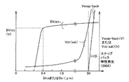
上記コレクタ構造を用いることで、正常なIGBTの動作を保障することができ、高い耐圧を保持することができ、IGBTの熱暴走を抑制することができる。また、デバイス特性を改善する際にN-ドリフト層を薄厚化した上で、VCE(sat)−EOFFのトレードオフ特性の自由度(制御性)を得ることができる。
IGBTの重要なデバイス特性であるVCE(sat)−Eoff特性を改善するためには、n-ドリフト層1の薄膜化を行なうことが有効である。しかし、図11に示すように半導体基板の第2主面を研磨する場合には、研磨面の表面粗さが、IGBTの種々の特性に影響を与えることを本願発明者は見出した。
本実施の形態においては、実施の形態1〜3の構成により得られる効果と同様の効果の得られるMOSトランジスタの構成を示す。
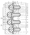
図43〜図78は、実施の形態4と同じ効果が得られるMOSトランジスタ構造の各種の派生構造を示す概略断面図である。図43〜図78に示すどの構造でも、実施の形態4に示すMOSトランジスタ構造による効果を得ることができる。
図43に示す構成は、2つのMOSトランジスタ部に挟まれる領域にエミッタ電位となる1つのエミッタトレンチが設けられている点およびゲート用溝1aの一方側面にのみn型エミッタ領域3が形成されている点において図40に示す構造Eの構成と異なる。
本実施の形態においては、図75〜図78に示す平面ゲート型IGBTの他の構成について説明する。図79〜図83は、本発明の実施の形態6における平面ゲート型IGBTの各種の構成を示す概略断面図である。
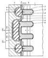
図87は、本発明の実施の形態7における半導体装置のレイアウトを示す平面図である。図88は、図87のLXXXVIII−LXVIII線に沿った断面図であり、図89は、図87のLXXXIX−LXXXIX線に沿った断面図である。図90は、図88のXC−XC線に沿った不純物濃度分布である。なお、図87において斜線で示す部分は、p型不純物拡散領域41が形成されている領域である。また、図87においては、1つのゲート電極配線11aに沿って形成されたゲート用溝1a(図中点線)のみを示しているが、実際には、それぞれのゲート電極配線11aに沿って複数のゲート用溝1a(あるいはエミッタ用溝1b)が形成されている。図87〜図90を参照して、本実施の形態におけるIGBTの構成について説明する。
図100は、本発明の実施の形態8におけるゲートパッドの平面レイアウトを模式的に示す図である。図100を参照して、本実施の形態においては、ゲート電極配線11a(図87)の電流経路の一部が、局所的に高い抵抗を有する抵抗体28aによって形成されている。図100では、配線(表面ゲート配線)とゲート電極配線11aとを電気的に接続するためのゲートパッド28の一部が抵抗体28aによって形成されている。抵抗体28aの各々は、ゲートパッド28の中央部に設けられた開口部において、互いに対向するように突き出ている。抵抗体28aはたとえば図1または図75に示すゲート電極5aと同一の構造を有していてもよい。
IGBTにおけるVCE(sat)−EOFF特性を向上するためには、n-ドリフト層1の厚みを薄くすることが効果的であるが、n-ドリフト層1の厚みを薄くすると、高耐圧を実現することが難しくなる。そこで本願発明者は、p型ボディ領域2とn型不純物拡散領域14との接合面の電界強度EP/CS(n型不純物拡散領域14が形成されていない場合にはp型ボディ領域2とn-ドリフト層1との接合面の電界強度EP/N-)と、n型バッファ領域7とn-ドリフト層1との接合面の電界強度EN/N-との関係に着目することで、IGBTの耐圧を向上できることを見出した。
Claims (1)
- 互いに対向する第1主面および第2主面を有する半導体基板と、
前記第1主面側に形成されたゲート電極(5a)と、前記第1主面側に形成された第1電極(11)と、前記第2主面に接触して形成された第2電極(12)とを有する素子とを備え、
前記素子は、前記ゲート電極に加えられる電圧によりチャネルに電界を発生させ、かつ前記チャネルの電界によって前記第1電極と前記第2電極との間の電流を制御し、
前記チャネルとなる第1導電型のボディ拡散層(2)と、
前記ボディ拡散層内に形成され、前記第1電極に接触する第2導電型のエミッタ拡散層(3)と、
前記第2主表面に形成され、第2導電型のドリフト拡散層(1)と第1導電型のコレクタ拡散層(8)とを含み、前記第2電極に電気的に接続されるコレクタ領域と、
前記ボディ拡散層と前記ドリフト拡散層との間に形成された第2導電型の埋込拡散層(14)と
を備え、
前記半導体基板の前記第1主面にはゲート用溝(1a)が形成されており、前記ゲート用溝(1a)内には前記ゲート電極(5a)が埋め込まれており、
前記半導体基板の前記第1主面には複数の溝(1a、1b)が形成されており、かつ前記複数の溝の各々は平面的に見て一の方向に配列しており、かつ前記ゲート用溝(1a)は前記複数の溝のうち少なくとも1つであり、
前記複数の溝の各々に隣接して前記第1の主面に形成され、かつ平面的に見て前記一の方向に延在し、かつ前記複数の溝の各々よりも深く形成された第1導電型のウェル層(41)をさらに備え、
前記半導体基板の厚さは50〜800μmであり、
前記ボディ拡散層の不純物濃度は1×1015cm−3〜1×1018cm−3、前記ボディ拡散層の前記第1主表面からの拡散深さは1.0μm〜4.0μmであり、
前記エミッタ拡散層の不純物濃度は1×1018cm−3〜1×1020cm−3、前記エミッタ拡散層の前記第1主表面からの拡散深さは0.3μm〜2.0μmであり、
前記ドリフト拡散層の不純物濃度は1×1012cm−3〜1×1015cm−3 であり、
前記埋込拡散層の不純物濃度は、前記ドリフト拡散層の不純物濃度よりも高い不純物濃度であり、
前記ゲート用溝の深さは3μm〜10μmであり、
前記溝は、前記埋込拡散層における不純物濃度が1×1016cm−3となる位置よりも前記第2主表面側に突出しており、
前記ゲート用溝の底面から前記ウェル層の底部までの深さ(DT,Pwell)は、0よりも
大きく1.0μm以下である、半導体装置。
Priority Applications (1)
| Application Number | Priority Date | Filing Date | Title |
|---|---|---|---|
| JP2014087359A JP5908524B2 (ja) | 2014-04-21 | 2014-04-21 | 半導体装置 |
Applications Claiming Priority (1)
| Application Number | Priority Date | Filing Date | Title |
|---|---|---|---|
| JP2014087359A JP5908524B2 (ja) | 2014-04-21 | 2014-04-21 | 半導体装置 |
Related Parent Applications (1)
| Application Number | Title | Priority Date | Filing Date |
|---|---|---|---|
| JP2010505147A Division JPWO2009122486A1 (ja) | 2008-03-31 | 2008-03-31 | 半導体装置 |
Related Child Applications (1)
| Application Number | Title | Priority Date | Filing Date |
|---|---|---|---|
| JP2016058154A Division JP6280148B2 (ja) | 2016-03-23 | 2016-03-23 | 半導体装置 |
Publications (2)
| Publication Number | Publication Date |
|---|---|
| JP2014158041A JP2014158041A (ja) | 2014-08-28 |
| JP5908524B2 true JP5908524B2 (ja) | 2016-04-26 |
Family
ID=51578693
Family Applications (1)
| Application Number | Title | Priority Date | Filing Date |
|---|---|---|---|
| JP2014087359A Active JP5908524B2 (ja) | 2014-04-21 | 2014-04-21 | 半導体装置 |
Country Status (1)
| Country | Link |
|---|---|
| JP (1) | JP5908524B2 (ja) |
Cited By (2)
| Publication number | Priority date | Publication date | Assignee | Title |
|---|---|---|---|---|
| US10026803B1 (en) | 2016-12-27 | 2018-07-17 | Mitsubishi Electric Corporation | Semiconductor device, power conversion device, and method of manufacturing semiconductor device |
| US11101133B2 (en) | 2018-08-17 | 2021-08-24 | Mitsubishi Electric Corporation | Semiconductor device and manufacturing method thereof |
Families Citing this family (6)
| Publication number | Priority date | Publication date | Assignee | Title |
|---|---|---|---|---|
| CN106062960B (zh) | 2014-09-30 | 2019-12-10 | 富士电机株式会社 | 半导体装置及半导体装置的制造方法 |
| JP6406454B2 (ja) | 2015-07-07 | 2018-10-17 | 富士電機株式会社 | 半導体装置 |
| WO2017010393A1 (ja) | 2015-07-16 | 2017-01-19 | 富士電機株式会社 | 半導体装置および半導体装置の製造方法 |
| JP6832645B2 (ja) * | 2016-07-20 | 2021-02-24 | ローム株式会社 | 半導体装置 |
| CN106783988A (zh) * | 2017-01-05 | 2017-05-31 | 江苏中科君芯科技有限公司 | 具有高抗短路能力的igbt器件 |
| DE112018003086T5 (de) * | 2017-11-13 | 2020-03-05 | Fuji Electric Co., Ltd. | Halbleitervorrichtung und verfahren zur herstellung einerhalbleitervorrichtung |
Family Cites Families (2)
| Publication number | Priority date | Publication date | Assignee | Title |
|---|---|---|---|---|
| JP3976374B2 (ja) * | 1997-07-11 | 2007-09-19 | 三菱電機株式会社 | トレンチmosゲート構造を有する半導体装置及びその製造方法 |
| WO2002061845A1 (en) * | 2001-02-01 | 2002-08-08 | Mitsubishi Denki Kabushiki Kaisha | Semiconductor device and method of manufacturing the same |
-
2014
- 2014-04-21 JP JP2014087359A patent/JP5908524B2/ja active Active
Cited By (2)
| Publication number | Priority date | Publication date | Assignee | Title |
|---|---|---|---|---|
| US10026803B1 (en) | 2016-12-27 | 2018-07-17 | Mitsubishi Electric Corporation | Semiconductor device, power conversion device, and method of manufacturing semiconductor device |
| US11101133B2 (en) | 2018-08-17 | 2021-08-24 | Mitsubishi Electric Corporation | Semiconductor device and manufacturing method thereof |
Also Published As
| Publication number | Publication date |
|---|---|
| JP2014158041A (ja) | 2014-08-28 |
Similar Documents
| Publication | Publication Date | Title |
|---|---|---|
| KR101191281B1 (ko) | 반도체장치 | |
| JP5908524B2 (ja) | 半導体装置 | |
| US10269946B2 (en) | Semiconductor device and method of manufacturing the same | |
| JP5025071B2 (ja) | 半導体装置およびその製造方法 | |
| US9614106B2 (en) | Semiconductor device | |
| JP5605073B2 (ja) | 半導体装置 | |
| JP5384878B2 (ja) | 半導体装置およびその製造方法 | |
| JP6289683B2 (ja) | 半導体装置 | |
| US10068999B2 (en) | Vertical power component | |
| JP6089818B2 (ja) | 半導体装置及びその製造方法 | |
| WO2017130374A1 (ja) | パワー半導体装置及びパワー半導体装置の製造方法 | |
| JP6280148B2 (ja) | 半導体装置 | |
| US20150144989A1 (en) | Power semiconductor device and method of manufacturing the same | |
| JP6513168B2 (ja) | 半導体装置 | |
| JP6026767B2 (ja) | 半導体装置およびその製造方法 | |
| JP2011176026A (ja) | 半導体素子の製造方法 | |
| TW201232781A (en) | Semiconductor device and method for manufacturing same | |
| WO2016001182A2 (en) | Semiconductor device | |
| JP2019057674A (ja) | 半導体装置 | |
| CN111295765A (zh) | 半导体装置 | |
| JP2004266298A (ja) | 縦型半導体装置 | |
| KR20150056433A (ko) | 전력 반도체 소자 및 그 제조 방법 | |
| JP2010147366A (ja) | 半導体装置 |
Legal Events
| Date | Code | Title | Description |
|---|---|---|---|
| A977 | Report on retrieval |
Free format text: JAPANESE INTERMEDIATE CODE: A971007 Effective date: 20150319 |
|
| A131 | Notification of reasons for refusal |
Free format text: JAPANESE INTERMEDIATE CODE: A131 Effective date: 20150324 |
|
| A521 | Request for written amendment filed |
Free format text: JAPANESE INTERMEDIATE CODE: A523 Effective date: 20150430 |
|
| A131 | Notification of reasons for refusal |
Free format text: JAPANESE INTERMEDIATE CODE: A131 Effective date: 20150602 |
|
| A521 | Request for written amendment filed |
Free format text: JAPANESE INTERMEDIATE CODE: A523 Effective date: 20150624 |
|
| TRDD | Decision of grant or rejection written | ||
| A01 | Written decision to grant a patent or to grant a registration (utility model) |
Free format text: JAPANESE INTERMEDIATE CODE: A01 Effective date: 20160223 |
|
| A61 | First payment of annual fees (during grant procedure) |
Free format text: JAPANESE INTERMEDIATE CODE: A61 Effective date: 20160323 |
|
| R150 | Certificate of patent or registration of utility model |
Ref document number: 5908524 Country of ref document: JP Free format text: JAPANESE INTERMEDIATE CODE: R150 |
|
| R250 | Receipt of annual fees |
Free format text: JAPANESE INTERMEDIATE CODE: R250 |
|
| R250 | Receipt of annual fees |
Free format text: JAPANESE INTERMEDIATE CODE: R250 |
|
| R250 | Receipt of annual fees |
Free format text: JAPANESE INTERMEDIATE CODE: R250 |
|
| R250 | Receipt of annual fees |
Free format text: JAPANESE INTERMEDIATE CODE: R250 |
|
| R250 | Receipt of annual fees |
Free format text: JAPANESE INTERMEDIATE CODE: R250 |
|
| R250 | Receipt of annual fees |
Free format text: JAPANESE INTERMEDIATE CODE: R250 |