JP5908524B2 - Semiconductor device - Google Patents
Semiconductor device Download PDFInfo
- Publication number
- JP5908524B2 JP5908524B2 JP2014087359A JP2014087359A JP5908524B2 JP 5908524 B2 JP5908524 B2 JP 5908524B2 JP 2014087359 A JP2014087359 A JP 2014087359A JP 2014087359 A JP2014087359 A JP 2014087359A JP 5908524 B2 JP5908524 B2 JP 5908524B2
- Authority
- JP
- Japan
- Prior art keywords
- type
- region
- emitter
- main surface
- gate
- Prior art date
- Legal status (The legal status is an assumption and is not a legal conclusion. Google has not performed a legal analysis and makes no representation as to the accuracy of the status listed.)
- Active
Links
- 239000004065 semiconductor Substances 0.000 title claims description 101
- 238000009792 diffusion process Methods 0.000 claims description 136
- 239000012535 impurity Substances 0.000 claims description 134
- 239000000758 substrate Substances 0.000 claims description 54
- 230000005684 electric field Effects 0.000 claims description 23
- 239000010410 layer Substances 0.000 description 185
- 229910052698 phosphorus Inorganic materials 0.000 description 63
- 210000000746 body region Anatomy 0.000 description 59
- 238000010586 diagram Methods 0.000 description 36
- 230000015556 catabolic process Effects 0.000 description 34
- 229910021332 silicide Inorganic materials 0.000 description 26
- FVBUAEGBCNSCDD-UHFFFAOYSA-N silicide(4-) Chemical compound [Si-4] FVBUAEGBCNSCDD-UHFFFAOYSA-N 0.000 description 26
- 238000000034 method Methods 0.000 description 23
- 229910052757 nitrogen Inorganic materials 0.000 description 21
- 229910052751 metal Inorganic materials 0.000 description 20
- 239000002184 metal Substances 0.000 description 20
- VYPSYNLAJGMNEJ-UHFFFAOYSA-N Silicium dioxide Chemical compound O=[Si]=O VYPSYNLAJGMNEJ-UHFFFAOYSA-N 0.000 description 17
- 229910052814 silicon oxide Inorganic materials 0.000 description 17
- 230000004888 barrier function Effects 0.000 description 16
- 238000004519 manufacturing process Methods 0.000 description 16
- 239000000463 material Substances 0.000 description 16
- 238000009826 distribution Methods 0.000 description 12
- 230000000694 effects Effects 0.000 description 11
- 230000002829 reductive effect Effects 0.000 description 11
- 230000008569 process Effects 0.000 description 10
- 230000004913 activation Effects 0.000 description 9
- 238000005468 ion implantation Methods 0.000 description 9
- 230000002159 abnormal effect Effects 0.000 description 8
- 229910052717 sulfur Inorganic materials 0.000 description 8
- 238000000137 annealing Methods 0.000 description 7
- 238000005224 laser annealing Methods 0.000 description 7
- 230000004048 modification Effects 0.000 description 6
- 238000012986 modification Methods 0.000 description 6
- 230000010355 oscillation Effects 0.000 description 6
- 230000003647 oxidation Effects 0.000 description 6
- 238000007254 oxidation reaction Methods 0.000 description 6
- 229910052720 vanadium Inorganic materials 0.000 description 6
- 238000010438 heat treatment Methods 0.000 description 5
- IJGRMHOSHXDMSA-UHFFFAOYSA-N Atomic nitrogen Chemical compound N#N IJGRMHOSHXDMSA-UHFFFAOYSA-N 0.000 description 4
- OAICVXFJPJFONN-UHFFFAOYSA-N Phosphorus Chemical compound [P] OAICVXFJPJFONN-UHFFFAOYSA-N 0.000 description 4
- 229910008484 TiSi Inorganic materials 0.000 description 4
- 238000005229 chemical vapour deposition Methods 0.000 description 4
- 230000007547 defect Effects 0.000 description 4
- 238000005530 etching Methods 0.000 description 4
- 239000007769 metal material Substances 0.000 description 4
- 239000011574 phosphorus Substances 0.000 description 4
- 229910021420 polycrystalline silicon Inorganic materials 0.000 description 4
- 230000002441 reversible effect Effects 0.000 description 4
- 229910045601 alloy Inorganic materials 0.000 description 3
- 239000000956 alloy Substances 0.000 description 3
- 229910052782 aluminium Inorganic materials 0.000 description 3
- 229910052799 carbon Inorganic materials 0.000 description 3
- 230000005669 field effect Effects 0.000 description 3
- 150000002500 ions Chemical class 0.000 description 3
- 238000000206 photolithography Methods 0.000 description 3
- 238000005498 polishing Methods 0.000 description 3
- 239000005368 silicate glass Substances 0.000 description 3
- 239000010936 titanium Substances 0.000 description 3
- 229910000789 Aluminium-silicon alloy Inorganic materials 0.000 description 2
- XUIMIQQOPSSXEZ-UHFFFAOYSA-N Silicon Chemical compound [Si] XUIMIQQOPSSXEZ-UHFFFAOYSA-N 0.000 description 2
- -1 aluminum compound Chemical class 0.000 description 2
- 239000000969 carrier Substances 0.000 description 2
- 230000008859 change Effects 0.000 description 2
- 230000006378 damage Effects 0.000 description 2
- 230000007423 decrease Effects 0.000 description 2
- 230000003247 decreasing effect Effects 0.000 description 2
- 230000020169 heat generation Effects 0.000 description 2
- 238000002161 passivation Methods 0.000 description 2
- 238000001020 plasma etching Methods 0.000 description 2
- 239000003870 refractory metal Substances 0.000 description 2
- 229910052710 silicon Inorganic materials 0.000 description 2
- 239000010703 silicon Substances 0.000 description 2
- 229910019001 CoSi Inorganic materials 0.000 description 1
- 229910004298 SiO 2 Inorganic materials 0.000 description 1
- 238000009825 accumulation Methods 0.000 description 1
- 230000002411 adverse Effects 0.000 description 1
- XAGFODPZIPBFFR-UHFFFAOYSA-N aluminium Chemical compound [Al] XAGFODPZIPBFFR-UHFFFAOYSA-N 0.000 description 1
- 230000002238 attenuated effect Effects 0.000 description 1
- 238000006243 chemical reaction Methods 0.000 description 1
- 239000002131 composite material Substances 0.000 description 1
- 239000012141 concentrate Substances 0.000 description 1
- 239000013256 coordination polymer Substances 0.000 description 1
- 239000013078 crystal Substances 0.000 description 1
- 238000005516 engineering process Methods 0.000 description 1
- 239000007943 implant Substances 0.000 description 1
- 238000002513 implantation Methods 0.000 description 1
- 230000002401 inhibitory effect Effects 0.000 description 1
- 238000002347 injection Methods 0.000 description 1
- 239000007924 injection Substances 0.000 description 1
- 230000007257 malfunction Effects 0.000 description 1
- 238000005259 measurement Methods 0.000 description 1
- 229910044991 metal oxide Inorganic materials 0.000 description 1
- 150000004706 metal oxides Chemical class 0.000 description 1
- 229910052759 nickel Inorganic materials 0.000 description 1
- 238000000059 patterning Methods 0.000 description 1
- 239000002356 single layer Substances 0.000 description 1
- 239000000243 solution Substances 0.000 description 1
- 238000004544 sputter deposition Methods 0.000 description 1
- 239000000126 substance Substances 0.000 description 1
- 230000003746 surface roughness Effects 0.000 description 1
- 230000008646 thermal stress Effects 0.000 description 1
- 229910052719 titanium Inorganic materials 0.000 description 1
- 229910021341 titanium silicide Inorganic materials 0.000 description 1
- 230000001052 transient effect Effects 0.000 description 1
- WFKWXMTUELFFGS-UHFFFAOYSA-N tungsten Chemical compound [W] WFKWXMTUELFFGS-UHFFFAOYSA-N 0.000 description 1
- 229910052721 tungsten Inorganic materials 0.000 description 1
- 239000010937 tungsten Substances 0.000 description 1
Images


Description
本発明は半導体装置に関し、より特定的には、高耐圧半導体装置であるIGBT(Insulated Gate Bipolar Transistor)を備える半導体装置に関する。 The present invention relates to a semiconductor device, and more particularly to a semiconductor device including an IGBT (Insulated Gate Bipolar Transistor) which is a high voltage semiconductor device.
数百Vを超える電圧を制御する高耐圧半導体装置(パワーデバイス)の分野では、その取扱う電流も大きなことから、発熱、すなわち損失を抑えた素子特性が要求される。また、それらの電圧・電流を制御するゲートの駆動方式としては、駆動回路が小さく、そこでの損失の小さな電圧駆動素子が望ましい。 In the field of a high voltage semiconductor device (power device) that controls a voltage exceeding several hundred volts, a large amount of current is handled, so that element characteristics that suppress heat generation, that is, loss are required. Further, as a gate driving system for controlling these voltages and currents, a voltage driving element having a small driving circuit and a small loss is desirable.
近年、上記のような理由で、この分野では電圧駆動が可能で、損失の少ない素子として、絶縁ゲートバイポーラトランジスタ、すなわちIGBTが主流となってきている。このIGBTの構造は、MOS(Metal Oxide Semiconductor)トランジスタのドレインの不純物濃度を低くして耐圧を保たせるとともに、ドレイン抵抗を低くするためにドレイン側をダイオードとしたものとみなすことができる構造である。 In recent years, an insulated gate bipolar transistor, that is, an IGBT, has become the mainstream as an element that can be driven by voltage and has little loss in this field for the reasons described above. The structure of this IGBT is a structure in which the drain side of a MOS (Metal Oxide Semiconductor) transistor has a low impurity concentration to maintain a breakdown voltage, and the drain side can be regarded as a diode in order to reduce the drain resistance. .
このようなIGBTにおいてはダイオードがバイポーラ動作をするため、本願においては、IGBTのMOSトランジスタのソース側をエミッタ側と呼び、ドレイン側をコレクタ側と呼ぶ。 In such an IGBT, since the diode performs a bipolar operation, in this application, the source side of the MOS transistor of the IGBT is called the emitter side, and the drain side is called the collector side.
電圧駆動素子であるIGBTでは一般に、コレクタとエミッタ間に数百Vの電圧が印加され、その電圧が±数V〜数十Vのゲート電圧によって制御される。また、IGBTはインバータとして用いられることが多く、ゲートがオン状態にある場合にはコレクタ・エミッタ間の電圧は低いが、大電流が流れ、ゲートがオフ状態にある場合には電流は流れないがコレクタ・エミッタ間の電圧は高くなっている。 In an IGBT which is a voltage driving element, a voltage of several hundreds V is generally applied between a collector and an emitter, and the voltage is controlled by a gate voltage of ± several V to several tens V. IGBTs are often used as inverters. When the gate is on, the collector-emitter voltage is low, but a large current flows, and when the gate is off, no current flows. The collector-emitter voltage is high.
通常は、上記のようなモードでIGBTの動作が行なわれるため、損失はオン状態での電流・電圧積である定常損失と、オン状態とオフ状態とが切替わる過渡時のスイッチング損失とに分けられる。オフ状態でのリーク電流・電圧積は非常に小さいため無視することができる。 Normally, since the IGBT is operated in the above-described mode, the loss is divided into a steady loss which is a current / voltage product in an on state, and a switching loss in a transient in which an on state and an off state are switched. It is done. The leakage current / voltage product in the off state is very small and can be ignored.
一方、たとえば負荷が短絡した場合など異常な状態にあっても、素子の破壊を防ぐことも重要である。この場合は、コレクタ・エミッタ間に数百Vの電源電圧が印加されたまま、ゲートがオンし、大電流が流れることになる。 On the other hand, it is important to prevent destruction of the element even in an abnormal state such as when the load is short-circuited. In this case, the gate is turned on and a large current flows while a power supply voltage of several hundred volts is applied between the collector and the emitter.
MOSトランジスタとダイオードとを直列に接続した構造を持つIGBTでは、MOSトランジスタの飽和電流で最大電流が制限される。このため、上記のような短絡時にも電流制限が働き、一定の時間発熱することによる素子の破壊を防ぐことができる。 In an IGBT having a structure in which a MOS transistor and a diode are connected in series, the maximum current is limited by the saturation current of the MOS transistor. For this reason, the current limit works even at the time of the short circuit as described above, and it is possible to prevent the element from being destroyed due to heat generation for a certain time.
従来のIGBTの構造は、たとえば特開2004−247593号公報(特許文献1)に開示されている。特許文献1のIGBTは、ゲート電極と、ソース(エミッタ)電極と、ドレイン(コレクタ)電極と、n型基板とを主に備えている。n型基板の上面にはトレンチが形成されており、ゲート電極はこのトレンチの内部に埋め込まれている。n型基板内の上部にはp型ベース層が形成されており、p型ベース層の内部にはn+型ソース層とp+型ドレイン層とが形成されている。n+型ソース層とp+型ドレイン層とはn型基板の表面において互いに隣接している。そしてゲート電極と、n+型ソース層およびp型ベース層とは、n型基板の内部においてゲート絶縁膜を挟んで対向している。エミッタ電極はn+型ソース層およびp+型ドレイン層と電気的に接触している。n型基板の下面にはp+型ドレイン層が形成されており、コレクタ電極はn型基板の下面側においてp+型ドレイン層に接触している。n型基板の内部におけるp型ベース層とp+型ドレイン層との間には、n-型エピタキシャル層およびn型バッファ層が埋め込まれている。n-型エピタキシャル層はp型ベース層およびn型バッファ層と接触しており、n型バッファ層はp+型ドレイン層と接触している。
A conventional IGBT structure is disclosed in, for example, Japanese Patent Application Laid-Open No. 2004-247593 (Patent Document 1). The IGBT of
また、特許文献1と同様の構造を有するIGBTは、たとえば特開2006−49933号公報(特許文献2)、特開2002−359373号公報(特許文献3)、特開平9−260662号公報(特許文献4)、米国特許第6,815,767号明細書(特許文献5)、米国特許第6,953,968号明細書(特許文献6)、および米国特許第6,781,199号明細書(特許文献7)にも開示されている。
Further, IGBTs having a structure similar to that of
パワーデバイスにおいては、1つのパッケージモジュール中に複数のIGBTおよびダイオードのチップを有しており、複数のIGBTは互いに並列に接続されている。パワーデバイスに使用されるIGBTの特性として重要なのが、オン電圧VCE(sat)の温度依存性である。ここでオン電圧VCE(sat)とは、任意の定格電流(密度)JCを得るために必要なコレクタ・エミッタ間の電圧である。オン電圧VCE(sat)の温度依存性が正、つまりIGBTの温度上昇とともにオン電圧VCE(sat)が大きくなることが、互いに並列に接続された複数のIGBTを動作させる(つまり、IGBTを並列的に動作させる)ことに適している。仮にオン電圧VCE(sat)の温度依存性が負であると、IGBTを並列的に動作させる場合に、オン電圧VCE(sat)の低いIGBTに電流が集中する。その結果、パッケージモジュールが誤作動を発生しやすくなり、破壊などの問題が起きやすくなる。 The power device has a plurality of IGBT and diode chips in one package module, and the plurality of IGBTs are connected in parallel to each other. An important characteristic of the IGBT used for the power device is the temperature dependence of the on-voltage V CE (sat). Here, the ON voltage V CE (sat) is a voltage between the collector and the emitter necessary for obtaining an arbitrary rated current (density) J C. When the temperature dependency of the on-voltage V CE (sat) is positive, that is, the on-voltage V CE (sat) increases as the temperature of the IGBT increases, a plurality of IGBTs connected in parallel with each other are operated (that is, the IGBT is Suitable for operation in parallel). If the temperature dependency of the on-voltage V CE (sat) is negative, when the IGBTs are operated in parallel, the current concentrates on the IGBT having a low on-voltage V CE (sat). As a result, the package module is likely to malfunction, and problems such as destruction are likely to occur.
従って、本発明の目的は、並列的な動作に適した半導体装置を得ることである。 Accordingly, an object of the present invention is to obtain a semiconductor device suitable for parallel operation.
本発明の一の局面に従う半導体装置は、半導体基板と素子とを備えている。半導体基板は、互いに対向する第1主面および第2主面を有している。素子は、第1主面側に形成されたゲート電極と、第1主面側に形成された第1電極と、第2主面に接触して形成された第2電極とを有している。素子は、ゲート電極に加えられる電圧によりチャネルに電界を発生させ、かつチャネルの電界によって第1電極と第2電極との間の電流を制御する。半導体基板と第2電極との界面におけるスパイクの密度は0以上3×10⁸個/cm2以下である。 A semiconductor device according to one aspect of the present invention includes a semiconductor substrate and an element. The semiconductor substrate has a first main surface and a second main surface that face each other. The element has a gate electrode formed on the first main surface side, a first electrode formed on the first main surface side, and a second electrode formed in contact with the second main surface. . The element generates an electric field in the channel by a voltage applied to the gate electrode, and controls a current between the first electrode and the second electrode by the electric field of the channel. The spike density at the interface between the semiconductor substrate and the second electrode is 0 or more and 3 × 10 8 pieces / cm 2 or less.
本発明の他の局面に従う半導体装置は、半導体基板と素子とを備えている。半導体基板は、互いに対向する第1主面および第2主面を有している。素子は、第1主面側に形成されたゲート電極と、第1主面側に形成された第1電極と、第2主面に接触して形成された第2電極とを有している。素子は、ゲート電極に加えられる電圧によりチャネルに電界を発生させ、かつチャネルの電界によって第1電極と第2電極との間の電流を制御する。半導体装置は第2主面に形成されたコレクタ領域をさらに備えている。コレクタ領域は、第2電極と接触する第1導電型のコレクタ拡散層と、コレクタ拡散層よりも第1主面側に形成された第2導電型のバッファ拡散層と、第2導電型のドリフト拡散層とを有している。ドリフト拡散層はバッファ拡散層よりも低い不純物濃度を有しており、かつバッファ拡散層と隣接してバッファ拡散層よりも第1主面側に形成されている。ドリフト拡散層を構成する不純物の単位面積あたりの原子数に対する前記バッファ拡散層を構成する不純物の単位面積あたりの原子数の比は0.05以上100以下である。 A semiconductor device according to another aspect of the present invention includes a semiconductor substrate and an element. The semiconductor substrate has a first main surface and a second main surface that face each other. The element has a gate electrode formed on the first main surface side, a first electrode formed on the first main surface side, and a second electrode formed in contact with the second main surface. . The element generates an electric field in the channel by a voltage applied to the gate electrode, and controls a current between the first electrode and the second electrode by the electric field of the channel. The semiconductor device further includes a collector region formed on the second main surface. The collector region includes a first conductivity type collector diffusion layer in contact with the second electrode, a second conductivity type buffer diffusion layer formed on the first main surface side of the collector diffusion layer, and a second conductivity type drift. And a diffusion layer. The drift diffusion layer has an impurity concentration lower than that of the buffer diffusion layer, and is formed adjacent to the buffer diffusion layer and closer to the first main surface than the buffer diffusion layer. The ratio of the number of atoms per unit area of the impurities constituting the buffer diffusion layer to the number of atoms per unit area of the impurities constituting the drift diffusion layer is 0.05 to 100.
本発明によれば、並列的な動作に適した半導体装置が得られる。 According to the present invention, a semiconductor device suitable for parallel operation can be obtained.
以下、本発明の実施の形態について図面に基づいて説明する。
(実施の形態1)
図1は、本発明の実施の形態1における半導体装置の構成を示す概略断面図である。図1を参照して、本実施の形態の半導体装置は、たとえば600〜6500Vの耐圧を有する半導体装置を想定すると、50〜800μmの厚みt1を有する半導体基板に形成されたトレンチ型IGBTである。半導体基板は互いに対向する第1主面(上面)および第2主面(下面)を有している。n-ドリフト層(ドリフト拡散層)1は、たとえば600〜6500Vの耐圧を有する半導体装置を想定すると、1×10¹²〜1×1015cm-3の濃度を有している。この半導体基板の第1主面側に、たとえば濃度が約1×10¹⁵〜1×1018cm-3で第1主面からの拡散深さが約1.0〜4.0μmのp型半導体よりなるp型ボディ領域2が形成されている。p型ボディ領域2(ボディ拡散層)内の第1主面には、たとえば濃度が1×10¹⁸〜1×1020cm-3で、第1主面からの拡散深さが約0.3〜2.0μmのn型半導体よりなるn型エミッタ領域3が形成されている。このn型エミッタ領域3(第2エミッタ拡散層)と隣り合うように第1主面には、p型ボディ領域2への低抵抗コンタクトをとるためのp+不純物拡散領域6(第1エミッタ拡散層)が、たとえば1×1018〜1×1020cm-3程度の濃度で、第1主面からの拡散深さがn型エミッタ領域3の深さ以下で形成されている。
Hereinafter, embodiments of the present invention will be described with reference to the drawings.
(Embodiment 1)
FIG. 1 is a schematic cross-sectional view showing the configuration of the semiconductor device according to the first embodiment of the present invention. Referring to FIG. 1, the semiconductor device of the present embodiment is a trench IGBT formed on a semiconductor substrate having a thickness t 1 of 50 to 800 μm, assuming a semiconductor device having a breakdown voltage of 600 to 6500 V, for example. . The semiconductor substrate has a first main surface (upper surface) and a second main surface (lower surface) that face each other. The n − drift layer (drift diffusion layer) 1 has a concentration of 1 × 10 12 to 1 × 10 15 cm −3 assuming a semiconductor device having a breakdown voltage of 600 to 6500 V, for example. On the first main surface side of the semiconductor substrate, for example, a p-type semiconductor having a concentration of about 1 × 10 15 to 1 × 10 18 cm −3 and a diffusion depth of about 1.0 to 4.0 μm from the first main surface. A p-
第1主面には、n型エミッタ領域3とp型ボディ領域2とを突き抜けてn-ドリフト層1に達するゲート用溝1aが形成されている。このゲート用溝1aは、第1主面からたとえば3〜10μmの深さを有しており、ゲート用溝1aのピッチは、たとえば2.0μm〜6.0μmである。このゲート用溝1aの内表面には、ゲート絶縁膜4aが形成されている。このゲート絶縁膜4aは、たとえばゲート絶縁膜の特性、信頼性およびデバイス歩留りを向上させる目的で、CVD法により形成されたシリコン酸化膜と熱酸化法により形成されたシリコン酸化膜もしくは窒素がSi/SiO2界面に偏析しているシリコン窒化酸化膜との積層構造を有している。
On the first main surface, there is formed a
ゲート用溝1a内を埋め込むように、たとえばリンが高濃度に導入された多結晶シリコンや、W/TiSi2などのメタル材料よりなるゲート電極5aが形成されている。なお、ゲート電極5aの低抵抗化のためにゲート電極5aの表面にシリサイド層(たとえばTiSi2、CoSiなど)が形成されていてもよい。このゲート電極5aの上面には、たとえばシリコン酸化膜よりなる絶縁膜22Aが形成されている。またゲート電極5aは、ゲート電位Gを与える制御電極に電気的に接続されている。なお、ゲート電極5aは第1主面側に形成されていればよい。
A
このようにゲート用溝1aとゲート絶縁膜4aとゲート電極5aとからゲートトレンチが構成されている。またn-ドリフト層1とn型エミッタ領域3とゲート電極5aとから、n-ドリフト層1をドレインとし、n型エミッタ領域3をソースとし、ゲート絶縁膜4aを挟んでゲート電極5aと対向するp型ボディ領域2の部分をチャネルとする絶縁ゲート型電界効果トランジスタ部(ここでは、MOSトランジスタ)が構成されている。すなわち、このMOSトランジスタは、ゲート電極5aに加えられる電圧によりチャネルに電界を発生させ、かつチャネルの電界によってエミッタ電極11とコレクタ電極12との間の電流を制御する。このMOSトランジスタが第1主面には複数個配置されている。
As described above, the
第1主面上には、たとえばシリケートガラスよりなる絶縁膜9と、CVD法により形成されたシリコン酸化膜よりなる絶縁膜22Bとが形成されており、これらの絶縁膜9、22Bには第1主面に達するコンタクトホール9aが設けられている。コンタクトホール9aの内表面および絶縁膜9、22Bの上面に沿うようにバリアメタル層10が形成されている。このバリアメタル層10と半導体基板との接する部分にはシリサイド層21aが形成されている。このバリアメタル層10およびシリサイド層21aを介して、n型エミッタ領域3およびp+不純物拡散領域6には、エミッタ電位Eを与えるエミッタ電極11(第1電極)が電気的に接続されている。なお、エミッタ電極11は第1主面側に形成されていればよい。
On the first main surface, an insulating
また、半導体基板の第2主面側にはp型コレクタ領域8(コレクタ拡散層)と、n型バッファ領域7(バッファ拡散層)とが形成されている。p型コレクタ領域8にはコレクタ電位Cを与えるコレクタ電極12(第2電極)が電気的に接続されている。コレクタ電極12は半導体基板の第2主面側に形成されており、コレクタ電位Cを与える。このコレクタ電極12の材質は、たとえばアルミニウム化合物である。n型バッファ領域7は、p型コレクタ領域8よりも第1主面側に形成されている。n-ドリフト層1はn型バッファ領域7よりも低い不純物濃度を有しており、かつn型バッファ領域7と隣接してn型バッファ領域7よりも第1主面側に位置している。p型コレクタ領域8と、n型バッファ領域7と、n-ドリフト層1とによりコレクタ領域が構成されている。
A p-type collector region 8 (collector diffusion layer) and an n-type buffer region 7 (buffer diffusion layer) are formed on the second main surface side of the semiconductor substrate. A collector electrode 12 (second electrode) for applying a collector potential C is electrically connected to the p-
特にn型バッファ領域7を設けることにより、n型バッファ領域7がない場合に比べて、主接合リーク特性が減少し、耐圧が上昇する。また、ターンオフ時のICの波形でテール電流が少なくなり、その結果、スイッチングロス(EOFF)が低減する。
In particular, by providing the n-
また、n型バッファ領域7の拡散深さが浅くなるのは、MOSトランジスタ側の不純物拡散領域が形成された後にn型バッファ領域7を形成するためである。すなわち、MOSトランジスタ側の不純物拡散領域への高温熱処理による悪影響を抑止するために、n型バッファ領域7を形成する際に、低温アニール技術、もしくはレーザアニールのように局所的に高温化するアニーリング技術を用いるためである。
The n-
本実施の形態の半導体装置においては、たとえばインバータ接続時には、エミッタ電位を基準に、制御電極のゲート電位Gはオフ状態では−15Vに、オン状態では+15Vに設定されたパルス状の制御信号であり、コレクタ電極12のコレクタ電位Cはゲート電位Gに従って概ね電源電圧と飽和電圧との間の電圧とされる。
In the semiconductor device of the present embodiment, for example, when the inverter is connected, the gate potential G of the control electrode is a pulsed control signal set to −15V in the off state and + 15V in the on state with the emitter potential as a reference. The collector potential C of the
次に、本実施の形態の製造方法について説明する。
図2〜図11は、本発明の実施の形態1における半導体装置の製造方法を工程順に示す概略断面図である。まず図2を参照して、n-ドリフト層1を含む半導体基板の第1主面に、たとえばピーク濃度が1×10¹⁵〜1×1018cm-3、第1主面からの拡散深さが1.0〜4.0μmのp型ボディ領域2が形成される。次に、第1主面上に、マスク層31が形成される。
Next, the manufacturing method of this embodiment will be described.
2 to 11 are schematic cross-sectional views showing the method of manufacturing the semiconductor device according to the first embodiment of the present invention in the order of steps. First, referring to FIG. 2, on the first main surface of the semiconductor substrate including n − drift layer 1, for example, the peak concentration is 1 × 10 15 to 1 × 10 18 cm −3 and the diffusion depth from the first main surface. Of p-
図3を参照して、マスク層31がパターニングされる。このパターニングされたマスク層31をマスクとして、たとえばイオン注入などが施されることにより、p型ボディ領域2内の第1主面に表面濃度が1.0×10¹⁸〜1.0×1020cm-3、第1主面からの拡散深さが0.3〜2.0μmのn型エミッタ領域3が形成される。この後、マスク層31が除去される。
Referring to FIG. 3,
図4を参照して、第1主面上に、たとえば熱酸化により形成されたシリコン酸化膜32と、CVD法により形成されたシリコン酸化膜33とが順に形成される。このシリコン酸化膜32、33が、通常の写真製版技術およびエッチング技術によりパターニングされる。このパターニングされたシリコン酸化膜32、33をマスクとして半導体基板に異方性エッチングが施される。これにより、n型エミッタ領域3とp型ボディ領域2とを突き抜けてn-ドリフト層1に達するゲート用溝1aが形成される。
Referring to FIG. 4, a
図5を参照して、等方性プラズマエッチングおよび犠牲酸化などの処理を行なうことにより、ゲート用溝1aの開口部と底部とが丸くなり、かつゲート用溝1aの側壁の凹凸が平坦化される。また上記の犠牲酸化により、ゲート用溝1aの内表面に犠牲酸化膜32aが熱酸化膜32と一体化するように形成される。このように等方性プラズマエッチングおよび犠牲酸化を施すことにより、ゲート用溝1aの内表面に形成されるゲート絶縁膜の特性を向上させることが可能となる。この後、酸化膜32、32a、33が除去される。
Referring to FIG. 5, by performing processing such as isotropic plasma etching and sacrificial oxidation, the opening and bottom of
図6を参照して、上記酸化膜の除去により、半導体基板の第1主面およびゲート用溝1aの内表面が露出する。
Referring to FIG. 6, by removing the oxide film, the first main surface of the semiconductor substrate and the inner surface of
図7を参照して、ゲート用溝1aの内表面および第1主面に沿うように、たとえばシリコン酸化膜よりなるゲート絶縁膜4aが形成される。ゲート用溝1a内を埋め込むように、たとえばリンが高濃度に導入された多結晶シリコンもしくは不純物の導入されていない多結晶シリコンにリンがイオン注入により導入された材料や、W(タングステン)/TiSi2(チタンシリサイド)などのメタル材料からなる導電層5が表面全面に形成される。
Referring to FIG. 7,
なおゲート絶縁膜4aとしては、ゲート絶縁膜としての特性、信頼性およびデバイス歩留まりを向上させる目的で、CVD法により形成したシリコン酸化膜と熱酸化により形成したシリコン酸化膜もしくは窒素がシリコンと酸化シリコンとの界面に偏析した窒化酸化膜とからなる積層構造が用いられることが好ましい。
As the
この後、通常の写真製版技術およびエッチング技術により、導電層5がパターニングされる。
Thereafter, the
図8を参照して、このパターニングにより、導電層がゲート用溝1a内に残存されてゲート電極5aが形成される。ここで、ゲート電極5aの低抵抗化のためにゲート電極5aの表面にシリサイド層(たとえばTiSi2、COSiなど)が形成されてもよい。この後、ゲート電極5aの上面が酸化されることにより、たとえばシリコン酸化膜よりなる絶縁膜22Aが形成される。この後、たとえば第1主面における表面濃度が1.0×10¹⁸〜1.0×1020cm-3、第1主面からの拡散深さがn型エミッタ領域3よりも浅いp+不純物拡散領域6が形成される。
Referring to FIG. 8, by this patterning, the conductive layer remains in
図9を参照して、第1主面上にたとえばシリケートガラスよりなる絶縁膜9と、CVD法により形成したシリコン酸化膜よりなる絶縁膜22Bとが順に形成される。この絶縁膜9、22Bに、通常の写真製版技術およびエッチング技術によりコンタクトホール9aが形成される。
Referring to FIG. 9, an insulating
図10を参照して、たとえば金属層よりなるバリアメタル層10がスパッタリング法により形成される。この後、ランプアニールが施されてバリアメタル層10と半導体基板との接触部にシリサイド層21aが形成される。この後、エミッタ電極11が形成される。
Referring to FIG. 10,
図11を参照して、半導体基板の第2主面側のn-ドリフト層1が研磨される。この研磨により、半導体基板の厚みt1は、MOSトランジスタの必要な耐圧に応じて調整される。たとえば600V〜6500Vの耐圧を有するIGBTを製造するには、n-ドリフト層1の厚みt3(図1)は50〜800μmとなる。研磨後は、研磨された面の結晶性を回復するために、半導体基板の第2主面のエッチングなどが行なわれる。 Referring to FIG. 11, n − drift layer 1 on the second main surface side of the semiconductor substrate is polished. By this polishing, the thickness t 1 of the semiconductor substrate is adjusted according to the required breakdown voltage of the MOS transistor. For example, to manufacture an IGBT having a withstand voltage of 600V to 6500V, the thickness t 3 (FIG. 1) of the n − drift layer 1 is 50 to 800 μm. After the polishing, the second main surface of the semiconductor substrate is etched to recover the crystallinity of the polished surface.
その後、半導体基板の第2主面にたとえばイオン注入法によりn型不純物およびp型不純物を注入した後に、不純物を拡散させる。もしくは、n型不純物およびp型不純物を注入した直後に、それぞれの不純物の注入深さに応じた熱処理を行なう。その結果、n型バッファ領域7およびp型コレクタ領域8が形成される。さらにコレクタ電極12が形成されて図1に示す半導体装置が完成する。コレクタ電極12は、たとえばアルミニウムその他の、p型コレクタ領域8とのオーミック接触性が得られるメタル材料からなる。
Thereafter, n-type impurities and p-type impurities are implanted into the second main surface of the semiconductor substrate by, for example, ion implantation, and then the impurities are diffused. Alternatively, immediately after the n-type impurity and the p-type impurity are implanted, a heat treatment according to the implantation depth of each impurity is performed. As a result, an n-
なお、本実施の形態においては、図11に示すようにエミッタ電極11を形成した後にn-ドリフト層1の第2主面を研磨し、n型バッファ領域7およびp型コレクタ領域8を形成してもよい。また、図2に示すようにp型ボディ領域2を形成する前に第2主面を研磨してもよい。また、図9に示すようにコンタクトホール9aの開口後もしくは開口前に第2主面を研磨し、n型バッファ領域7およびp型コレクタ領域8を形成してもよい。
In the present embodiment, as shown in FIG. 11, after the
本実施の形態において、半導体基板とコレクタ電極12との界面におけるスパイク密度(p型コレクタ領域8を形成する半導体材料とコレクタ電極12中のp型コレクタ領域8側のメタル材料との反応により形成される合金からなるスパイクの密度)は0以上3×10⁸個/cm2以下である。
In the present embodiment, the spike density at the interface between the semiconductor substrate and the collector electrode 12 (formed by the reaction between the semiconductor material forming the p-
図12および図13は、スパイクが形成されたp型コレクタ領域とコレクタ電極との界面の状態を模式的に示す図である。図12は断面図、図13は平面図である。図12および図13を参照して、p型コレクタ領域8とコレクタ電極12との界面には、通常、複数のスパイクが形成されている。スパイクとは、コレクタ電極12を構成する材料とp型コレクタ領域8を構成する材料との合金よりなる、たとえば四角錐や八角錐の形状を有する突起(または凹部)である。ここで、コレクタ電極12が多層膜で形成されている場合には、スパイクは、p型コレクタ領域8に直接接触する層12aを構成する材料とp型コレクタ領域8を構成する材料との合金より形成される。
12 and 13 are diagrams schematically showing the state of the interface between the p-type collector region where the spike is formed and the collector electrode. 12 is a cross-sectional view, and FIG. 13 is a plan view. Referring to FIGS. 12 and 13, a plurality of spikes are usually formed at the interface between p-
スパイク密度は、たとえば以下の方法によって測定される。始めに、薬液を用いてコレクタ電極12を溶解し、半導体基板から除去する。そして、露出された半導体基板の第2主面を顕微鏡で観察し、第2主面に存在する四角錐や八角錐などの凹部の個数を数える。その結果、得られた個数を観察した面積で割った値をスパイク密度と定義する。
The spike density is measured by the following method, for example. First, the
スパイク密度が大きくなると、低温(298K以下)でのp型コレクタ領域8の不純物のイオン化率が低下し、p型コレクタ領域8からn型バッファ領域7へのキャリア(ホール)の実効的な注入効率が低下する。このため、IGBTのJc−VCE特性はスパイク密度に依存する。
As the spike density increases, the ionization rate of impurities in the p-
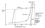
スパイク密度を0以上3×10⁸個/cm2以下とすることによって、以下の効果を得ることができる。図14は、本発明の実施の形態1におけるコレクタ・エミッタ間電圧と電流密度との関係の温度依存性を示す図である。図14を参照して、VCE(sat)は、任意の定格電流密度に対応するエミッタ・コレクタ間電圧である。298Kおよび398Kの温度では、スパイク密度が3×108個/cm2以上の場合であっても3×108個/cm2以下の場合であってもほぼ同じ曲線となっている。一方、233Kの温度では、スパイク密度が3×108個/cm2以下の場合のエミッタ・コレクタ間電圧が著しく増加している。 By setting the spike density to 0 or more and 3 × 10 8 pieces / cm 2 or less, the following effects can be obtained. FIG. 14 is a diagram showing the temperature dependence of the relationship between the collector-emitter voltage and the current density in the first embodiment of the present invention. Referring to FIG. 14, V CE (sat) is an emitter-collector voltage corresponding to an arbitrary rated current density. At temperatures of 298 K and 398 K, the curves are almost the same whether the spike density is 3 × 10 8 pieces / cm 2 or more or 3 × 10 8 pieces / cm 2 or less. On the other hand, at a temperature of 233 K, the emitter-collector voltage increases significantly when the spike density is 3 × 10 8 pieces / cm 2 or less.
図15は、本発明の実施の形態1におけるスパイク密度とオン電圧の変化量との関係を示す図である。図15は、p型コレクタ領域8およびn型バッファ領域7の条件(濃度、深さ)を一定にした場合の結果である。また、図15におけるオン電圧の変化量ΔVonは、298Kにおけるコレクタ・エミッタ間電圧VCE(sat)(298K)から233Kにおけるコレクタ・エミッタ間電圧VCE(sat)(233K)を引いた値である。図15を参照して、スパイク密度Dspikeが3×10⁸個/cm2以下の場合には、298Kにおけるコレクタ・エミッタ間電圧VCE(sat)は、233Kにおけるコレクタ・エミッタ間電圧VCE(sat)以上の値である。一方、スパイク密度Dspikeが3×108個/cm2を超える場合には、298Kにおけるコレクタ・エミッタ間電圧VCE(sat)は、233Kにおけるコレクタ・エミッタ間電圧VCE(sat)未満の値となる。
FIG. 15 is a diagram showing the relationship between the spike density and the amount of change in on-voltage in
図16は、本発明の実施の形態1におけるデバイスのオペレーション温度とコレクタ・エミッタ間電圧との関係のスパイク密度依存性を示す図である。図16を参照して、スパイク密度Dspikeが3×10⁸個/cm2以下の場合には、電圧VCE(sat)の温度依存性が正であるのに対して、スパイク密度Dspikeが3×108個/cm2以上の場合には、298K未満の領域で電圧VCE(sat)の温度依存性が負である。 FIG. 16 is a diagram showing the spike density dependence of the relationship between the device operating temperature and the collector-emitter voltage in the first embodiment of the present invention. Referring to FIG. 16, when the spike density D spike is 3 × 10 8 pieces / cm 2 or less, the temperature dependence of the voltage V CE (sat) is positive, whereas the spike density D spike is In the case of 3 × 10 8 pieces / cm 2 or more, the temperature dependence of the voltage V CE (sat) is negative in the region below 298K.
以上より、本実施の形態のように半導体基板とコレクタ電極12との界面におけるスパイク密度を0以上3×10⁸個/cm2以下とすることにより、コレクタ・エミッタ間電圧VCEの温度依存性を正にすることができる。その結果、IGBTを並列的に動作させる場合に、電圧VCEの低いIGBTへの電流の集中がなくなり、並列的な動作に適した半導体装置を得ることができる。
As described above, the temperature dependence of the collector-emitter voltage V CE is obtained by setting the spike density at the interface between the semiconductor substrate and the
スパイク密度は、たとえばコレクタ電極の材質、熱処理条件、またはコレクタ電極の膜厚によって制御することができる。コレクタ電極の材質としては、Al、AlSi、Ti、および金属を含むシリサイドが適している。金属を含むシリサイドとしては、Tiを含むシリサイド、Niを含むシリサイド、またはCoを含むシリサイドが挙げられる。また、コレクタ電極の材質としては、たとえばAlやAlSiなどの、接触する半導体層(図1ではp型コレクタ領域8)との間でオーミック抵抗性を示す材料が好ましい。半導体基板の材質としては、Si、SiC、GaN、またはGeが適している。特にコレクタ電極としてシリサイドを使用した場合には、半導体基板とコレクタ電極との界面にスパイクが存在しなくなる。シリサイドよりなるコレクタ電極は、Si、SiC、GaN、またはGeなどよりなる半導体基板の第2主面にTi、Co、またはNiなどよりなる金属を形成し、熱処理を施すことにより形成される。
The spike density can be controlled by, for example, the material of the collector electrode, the heat treatment conditions, or the thickness of the collector electrode. As a material for the collector electrode, Al, AlSi, Ti, and silicide containing metal are suitable. Examples of the silicide containing metal include a silicide containing Ti, a silicide containing Ni, and a silicide containing Co. The material of the collector electrode is preferably a material that exhibits ohmic resistance with the semiconductor layer (p-
また、コレクタ電極の膜厚は200nm以上であることが好ましい。図17は、本発明の実施の形態1におけるコレクタ電極の膜厚とスパイク密度との関係を示す図である。図17を参照して、コレクタ電極の膜厚が200nm以上である場合には、スパイク密度が3×10⁸個/cm2以下となっている。一方、製造限界の観点から、コレクタ電極の膜厚は10000nm以下であることが好ましい。 The film thickness of the collector electrode is preferably 200 nm or more. FIG. 17 is a diagram showing the relationship between the collector electrode thickness and the spike density in the first embodiment of the present invention. Referring to FIG. 17, when the collector electrode film thickness is 200 nm or more, the spike density is 3 × 10 8 pieces / cm 2 or less. On the other hand, from the viewpoint of production limit, the thickness of the collector electrode is preferably 10,000 nm or less.
上記のような、コレクタ電極の材質、熱処理条件、またはコレクタ電極の膜厚を適宜組み合わせることにより、スパイク密度を0以上3×10⁸個/cm2以下とすることができる。 The spike density can be set to 0 or more and 3 × 10 8 pieces / cm 2 or less by appropriately combining the material of the collector electrode, the heat treatment conditions, or the thickness of the collector electrode as described above.
なお、本実施の形態においては図1に示す構成を有するIGBTである場合について示した。しかし、本発明の半導体装置は、図1の構成のものに限定されず、互いに対向する第1主面および第2主面を有する半導体基板と、素子とを備えるものであればよい。この素子は、第1主面側に形成されたゲート電極と、第1主面側に形成された第1電極と、前記第2主面に接触して形成された第2電極とを有している。この素子は、ゲート電極に加えられる電圧によりチャネルに電界を発生させ、かつチャネルの電界によって第1電極と前記第2電極との間の電流を制御する。さらに、ダイオードのようなデバイス構造でもよい。 In the present embodiment, an IGBT having the configuration shown in FIG. 1 is shown. However, the semiconductor device of the present invention is not limited to the one having the configuration shown in FIG. 1, and any semiconductor device may be used provided it includes a semiconductor substrate having a first main surface and a second main surface facing each other and an element. This element has a gate electrode formed on the first main surface side, a first electrode formed on the first main surface side, and a second electrode formed in contact with the second main surface. ing. This element generates an electric field in the channel by a voltage applied to the gate electrode, and controls a current between the first electrode and the second electrode by the electric field of the channel. Furthermore, a device structure such as a diode may be used.
(実施の形態2)
図18は、図1のXVIII−XVIII線に沿った濃度分布である。図19は、図1のXIX−XIX線に沿った濃度分布である。なお、図18には、従来におけるp型不純物またはn型不純物の濃度分布もあわせて示されている。
(Embodiment 2)
FIG. 18 is a concentration distribution along the line XVIII-XVIII in FIG. FIG. 19 is a concentration distribution along the line XIX-XIX in FIG. FIG. 18 also shows a conventional concentration distribution of p-type impurities or n-type impurities.
図18および図19を参照して、濃度CS,Pは、コレクタ電極12とp型コレクタ領域8との界面(半導体基板の第2主面)におけるp型コレクタ領域8の不純物濃度であり、濃度CP,Pは、p型コレクタ領域8の不純物濃度の最大値である。濃度CP,Nは、n型バッファ領域7の不純物濃度の最大値である。濃度Csubは、n-ドリフト層1の不純物濃度である。深さDpは、p型コレクタ領域8とn型バッファ領域7との接合面までの第2主面からの深さである。深さDP,Nは、n型バッファ領域7における濃度CP,Nとなる位置までの第2主面からの深さである。深さDN-は、n型バッファ領域7とn-ドリフト層1との接合面までの第2主面からの深さである。なお、後述の図29で示すようにn型中間層7aが形成されている場合には、深さDNは、n型バッファ領域7とn型中間層7aとの接合面の第2主面からの深さである。τPはp型コレクタ領域8のキャリアライフタイムであり、τNはn型バッファ領域7のキャリアライフタイムであり、τN-はn-ドリフト層1のキャリアライフタイムである。τXは第2主面からxの深さにある位置のキャリアライフタイムである。SNはn型バッファ領域7を構成する不純物の単位面積あたりの原子数(atom/cm2)であり、SN-はn-ドリフト層1を構成する不純物の単位面積あたりの原子数(atom/cm2)である。所望の領域における不純物の単位面積あたりの原子数は、その領域における不純物濃度プロファイルを深さ方向全体にわたって積分することによって求められる。
Referring to FIGS. 18 and 19, the concentration C S, P is the impurity concentration of p-
本願発明者は、p型コレクタ領域8とn型バッファ領域7とn-ドリフト層1との関係を以下の条件とすることによって、IGBTの異常動作を抑止できることを見出した。ここで、IGBTの異常動作を抑止するとは、以下のことを意味している。
The inventor of the present application has found that the abnormal operation of the IGBT can be suppressed by setting the relationship among the p-
a.298K以下の温度でJc−VCE特性にスナップバック(snap back)特性が発生しないこと。 a. No snap back characteristics occur in the J c -V CE characteristics at temperatures below 298K.
b.298K以下の低温でもIGBTがオンすること。
c.所望の耐圧を有する、または398K以上においてIGBTが熱暴走しないこと。
b. The IGBT must be turned on even at a low temperature of 298K or lower.
c. The IGBT has a desired withstand voltage, or the IGBT does not run out of heat at 398K or higher.
図20は、本発明の実施の形態2におけるCP,P/CP,Nと、VCE(sat)およびターンオフ時のエネルギロスEOffとの関係を示す図である。EOffとは、スイッチングデバイスがターンオフする際のエネルギロスである。Vsnap-backとは、スナップバック特性が生じた場合の図22中に示すポイントAでのコレクタ・エミッタ間電圧である。図21は、本発明の実施の形態2におけるIGBTにおけるCP,P/CP,Nと、VCE(sat)およびリーク電流密度JCESとの関係を示す図である。リーク電流密度JCESとは、ゲート・エミッタ間をショートした状態でのコレクタ・エミッタ間のリーク電流密度である。図20および図21を参照して、n型バッファ領域7の不純物濃度の最大値に対するp型コレクタ領域8の不純物濃度の最大値の比CP,P/CP,NがCP,P/CP,N<1の場合には、スナップバック特性が発生し、それに伴なうスナップバック電圧Vsnap-backが発生する。その結果、図22に示すように、CP,P/CP,N<1の場合には、任意の電流密度に対するVCE(sat)が増加する。また、CP,P/CP,N>1×103の場合には、JCESが増加し、IGBTの熱暴走が発生する。以上より、IGBTの異常動作を抑止するためには、1≦CP,P/CP,N≦1×103であることが好ましい。
FIG. 20 is a diagram showing the relationship between C P, P / C P, N and V CE (sat) and the energy loss E Off during turn-off in the second embodiment of the present invention. E Off is an energy loss when the switching device is turned off. V snap-back is the collector-emitter voltage at point A shown in FIG. 22 when the snap-back characteristic occurs. FIG. 21 is a diagram showing a relationship between C P, P / C P, N and V CE (sat) and leakage current density J CES in the IGBT according to the second embodiment of the present invention. The leakage current density J CES is a leakage current density between the collector and the emitter in a state where the gate and the emitter are short-circuited. Referring to FIGS. 20 and 21, the ratio C P, P / C P, N of the maximum impurity concentration of p-
図23は、本発明の実施の形態2におけるSN/SN-と、VCE(sat)および降伏電圧BVCESとの関係を示す図である。降伏電圧BVCESとは、コレクタ・エミッタ間をショートさせた状態でのコレクタ・エミッタ間の降伏電圧である。図23を参照して、n-ドリフト層1を構成する不純物の単位面積あたりの原子数(atom/cm2)に対するn型バッファ領域7を構成する不純物の単位面積あたりの原子数(atom/cm2)の比SN/SN-が0.05≦SN/SN-の場合には、高い降伏電圧BVCESが得られている。また、SN/SN-がSN/SN-≦100の場合には、スナップバック特性が抑制されており、かつエミッタ・コレクタ間電圧VCE(sat)も低く抑えられている。以上より、IGBTの異常動作を抑止し、並列動作を可能とするためには、0.05≦SN/SN-≦100であることが好ましい。
FIG. 23 is a diagram showing a relationship between S N / S N− , V CE (sat), and breakdown voltage BV CES in the second embodiment of the present invention. The breakdown voltage BV CES is a breakdown voltage between the collector and the emitter in a state where the collector and the emitter are short-circuited. Referring to FIG. 23, the number of atoms per unit area (atom / cm 2 ) of impurities constituting n-
図24は、本発明の実施の形態2におけるCS,PおよびCP,Pと、VCE(sat)との関係の温度依存性を示す図である。図24を参照して、233K、298K、および398Kいずれの温度の場合でも、5×10¹⁵≦CS,P、1×10¹⁶≦CP,Pとすることで、エミッタ・コレクタ間電圧VCE(sat)が大きく低下している。また、製造限界を考慮すると、CS,P≦1.0×1022cm-3、CP,P≦1.0×1022cm-3であることが好ましい。 FIG. 24 is a diagram showing the temperature dependence of the relationship between C S, P and C P, P and V CE (sat) in the second embodiment of the present invention. Referring to FIG. 24, the emitter-collector voltage V can be obtained by setting 5 × 10 15 ≦ C S, P and 1 × 10 16 ≦ C P, P at any temperature of 233 K, 298 K, and 398 K. CE (sat) has dropped significantly. In consideration of the production limit, C S, P ≦ 1.0 × 10 22 cm −3 and C P, P ≦ 1.0 × 10 22 cm −3 are preferable.
図25は、本発明の実施の形態2におけるデバイスのオペレーション温度とVCE(sat)との関係のCS,PおよびCP,P依存性を示す図である。図26および図27は、本発明の実施の形態2におけるJC−VCE特性の温度依存性を示す図である。図24〜図27を参照して、5×10¹⁵≦CS,P、1×10¹⁶≦CP,Pの場合にはVCE(sat)の温度依存性が正になることが分かる。 FIG. 25 is a diagram showing the C S, P and C P, P dependence of the relationship between the device operating temperature and V CE (sat) in the second embodiment of the present invention. 26 and 27 are diagrams showing the temperature dependence of the J C -V CE characteristics in the second embodiment of the present invention. 24 to 27, it can be seen that the temperature dependence of V CE (sat) becomes positive when 5 × 10 15 ≦ C S, P and 1 × 10 16 ≦ C P, P.
以上より、IGBTの異常動作を抑止するためには、5×10¹⁵≦CS,P、1×10¹⁶≦CP,Pであることが好ましい。 From the above, it is preferable that 5 × 10 15 ≦ C S, P and 1 × 10 16 ≦ C P, P to suppress the abnormal operation of the IGBT.
図28は、本発明の実施の形態2におけるDP,NまたはDN-と、VCE(sat)およびBVCESとの関係を示す図である。図28を参照して、n型バッファ領域7における濃度CP,Nとなる位置までの第2主面からの深さDP,Nが0.4μm≦DP,Nの場合、またはn型バッファ領域7とn-ドリフト層1との接合面の第2主面からの深さDN-が0.4μm≦DN-の場合には、高い降伏電圧BVCESおよび低いエミッタ・コレクタ間電圧VCE(sat)が得られている。一方、DP,N>50μmの場合またはDN->50μmの場合には、スナップバック特性が発生している。
FIG. 28 is a diagram showing a relationship between D P, N or D N− and V CE (sat) and BV CES in the second embodiment of the present invention. Referring to FIG. 28, the depth D P, N from the second main surface up to the position where the concentration C P, N in n-
以上より、IGBTの異常動作を抑止するためには、0.4μm≦DP,N≦50μm、0.4μm≦DN-≦50μmであることが好ましい。 From the above, in order to suppress the abnormal operation of the IGBT, it is preferable that 0.4 μm ≦ D P, N ≦ 50 μm and 0.4 μm ≦ D N− ≦ 50 μm.
図29は、図1のXVIII−XVIII線に沿った濃度分布の他の例である。図29を参照して、コレクタ領域はn型中間層7aをさらに有していてもよい。n型中間層7aの不純物濃度の最大値CP,N*は、n型バッファ領域7の不純物濃度の最大値CP,Nよりも低く、n-ドリフト層1の不純物濃度Csubよりも高い。またn型中間層7aは、n型バッファ領域7およびn-ドリフト層1の両方に接触している。深さDNは、n型バッファ領域7とn型中間層7aとの接合面の第2主面からの深さである。深さDN*は、n型中間層7aとn-ドリフト層1との接合面の第2主面からの深さである。SN*はn型中間層7aを構成する不純物の単位面積あたりの原子数(atom/cm2)である。n型中間層7aは、n型バッファ領域7の一部へ不純物イオンを注入することによって形成されてもよい。また、プロトンの照射などの方法で、ライフタイムキラーとなる結晶欠陥を生成するイオンをn型バッファ領域7の一部へ注入することによって形成されてもよい。
FIG. 29 is another example of the concentration distribution along the line XVIII-XVIII in FIG. Referring to FIG. 29, the collector region may further include an n-type
図30は、本発明の実施の形態2におけるSN*/SNとVCE(sat)との関係を示す図である。図30を参照して、n型バッファ領域7を構成する不純物の単位面積あたりの原子数(atom/cm2)に対するn型中間層7aを構成する不純物の単位面積あたりの原子数(atom/cm2)の比SN*/SNが0.5<SN*/SNの場合に、スナップバック特性が発生している。
FIG. 30 is a diagram showing the relationship between S N * / S N and V CE (sat) in the second embodiment of the present invention. Referring to FIG. 30, the number of atoms per unit area (atoms / cm 2 ) of impurities constituting n-type
以上より、IGBTの異常動作を抑止するためには、0<SN*/SN≦0.5であることが好ましい。 From the above, in order to suppress the abnormal operation of the IGBT, it is preferable that 0 <S N * / S N ≦ 0.5.
図31は、本発明の実施の形態2における第2主面からの深さxとVCE(sat)との関係を示す図である。図32は、本発明の実施の形態2におけるτx/τN-とVCE(sat)との関係を示す図である。図33は、本発明の実施の形態2における第2主面からの深さxとキャリアライフタイムとの関係の一例を示す図である。特に図33を参照して、第2主面近傍の半導体基板内には、p型コレクタ領域8およびn型バッファ領域7を形成するためのイオン注入の際に欠陥が導入される。n型バッファ領域7を形成する際にはp型コレクタ領域8を形成する際よりも深く不純物を注入する必要があるため、n型バッファ領域7はp型コレクタ領域8よりも高温でアニールする必要がある。その結果、n型バッファ領域7にアニールによる熱ストレスが発生し、n型バッファ領域7のキャリアライフタイムτNはp型コレクタ領域8のキャリアライフタイムτPよりも低くなる。また、n型バッファ領域7およびp型コレクタ領域8のキャリアライフタイムは、n-ドリフト層1のキャリアライフタイムτN-よりも低くなる。
FIG. 31 is a diagram showing the relationship between the depth x from the second principal surface and V CE (sat) in the second embodiment of the present invention. FIG. 32 shows the relationship between τ x / τ N− and V CE (sat) in the second embodiment of the present invention. FIG. 33 is a diagram showing an example of the relationship between the depth x from the second principal surface and the carrier lifetime in
そこで、特に第2主面からの深さxが0.50μm≦x≦60.0μmである領域において、n-ドリフト層1のキャリアライフタイムτN-に対する第2主面から深さxの位置のキャリアライフタイムτxの比τx/τN-を、1×10-6≦τx/τN-≦1とすることにより、特に図31および図32に示すように、コレクタ・エミッタ間電圧VCE(sat)が著しく低減される。 Therefore, particularly in a region where the depth x from the second main surface is 0.50 μm ≦ x ≦ 60.0 μm, the position of the depth x from the second main surface with respect to the carrier lifetime τ N− of the n − drift layer 1. By setting the ratio τ x / τ N− of the carrier lifetime τ x of 1 × 10 −6 ≦ τ x / τ N− ≦ 1, particularly between the collector and the emitter as shown in FIGS. The voltage V CE (sat) is significantly reduced.
ここで、キャリアライフタイムが低下する原因は、p型コレクタ領域8およびn型バッファ領域7を形成する際のイオン注入の際に、p型コレクタ領域8およびn型バッファ領域7に欠陥が導入されることにある。キャリアライフタイムを向上するためには、欠陥が導入された部分をアニールする方法が有効である。次に、アニール技術とキャリアライフタイムとの関係を示す。
Here, the reason why the carrier lifetime is lowered is that defects are introduced into the p-
図34は、本発明の実施の形態2におけるレーザアニールの出力および拡散炉の温度と、キャリアライフタイムとの関係を示す図である。図34を参照して、拡散炉でアニールを行なう場合には、拡散炉の温度を高くしすぎるとキャリアライフタイムが低下する。また、レーザアニール技術において高出力エネルギでレーザアニールを行なう場合には、キャリアライフタイムの低下が起きる。また、レーザは半導体基板の内部で減衰する性質を有しているので、半導体基板の第2主面からp型コレクタ領域8とn型バッファ領域7との接合面までの深さが深すぎると、レーザアニールの出力を高くする必要があり、レーザアニールによってキャリアライフタイムを向上することが難しくなる。このことを考慮して、半導体基板の第2主面からp型コレクタ領域8とn型バッファ領域7との接合面までの深さは0より大きく1.0μm以下であることが好ましい。
FIG. 34 is a diagram showing the relationship between the laser annealing output and diffusion furnace temperature and the carrier lifetime in the second embodiment of the present invention. Referring to FIG. 34, when annealing is performed in a diffusion furnace, if the temperature of the diffusion furnace is increased too much, the carrier lifetime is lowered. In addition, when laser annealing is performed with high output energy in the laser annealing technique, the carrier lifetime is reduced. In addition, since the laser has a property of being attenuated inside the semiconductor substrate, if the depth from the second main surface of the semiconductor substrate to the junction surface between the p-
図35は、本発明の実施の形態2におけるイオン注入量と、キャリア活性化率、VCE(sat)およびBVCESとの関係を示す図である。図35を参照して、n型バッファ領域7およびp型コレクタ領域8の各々の活性化率は、n型バッファ領域7およびp型コレクタ領域8のイオン注入量、またはイオンの種類などに依存する。図35では、p型コレクタ領域8における活性化率とn型バッファ領域7における活性化率とが互いに異なっており、p型コレクタ領域8における活性化率はn型バッファ領域7における活性化率よりも低くなっている。これにより、IGBTが正常に動作し、降伏電圧BVCESを高くすることができる。特に、p型コレクタ領域8における活性化率が0より大きく90%以下である場合に、コレクタ・エミッタ間電圧VCE(sat)が大きく低減されている。
FIG. 35 is a diagram showing the relationship between the ion implantation amount, the carrier activation rate, V CE (sat), and BV CES in
なお、活性化率は、以下の式(1)にて算出される。
活性化率:{(SR(spreading-resistance)測定などの方法で算出される抵抗値より得られる不純物濃度(cm-3))/(SIMS(Secondary Ionization Mass Spectrometer)を用いて測定される不純物濃度(cm-3))}×100 ・・・(1)
上記コレクタ構造を用いることで、正常なIGBTの動作を保障することができ、高い耐圧を保持することができ、IGBTの熱暴走を抑制することができる。また、デバイス特性を改善する際にN-ドリフト層を薄厚化した上で、VCE(sat)−EOFFのトレードオフ特性の自由度(制御性)を得ることができる。
The activation rate is calculated by the following formula (1).
Activation rate: {(impurity concentration (cm −3 ) obtained from resistance value calculated by SR (spreading-resistance) measurement) / (impurity concentration measured using SIMS (Secondary Ionization Mass Spectrometer)) (Cm −3 ))} × 100 (1)
By using the collector structure, normal operation of the IGBT can be ensured, high breakdown voltage can be maintained, and thermal runaway of the IGBT can be suppressed. In addition, when the device characteristics are improved, the thickness of the N − drift layer is reduced, and the degree of freedom (controllability) of the trade-off characteristics of V CE (sat) −E OFF can be obtained.
(実施の形態3)
IGBTの重要なデバイス特性であるVCE(sat)−Eoff特性を改善するためには、n-ドリフト層1の薄膜化を行なうことが有効である。しかし、図11に示すように半導体基板の第2主面を研磨する場合には、研磨面の表面粗さが、IGBTの種々の特性に影響を与えることを本願発明者は見出した。
(Embodiment 3)
In order to improve the V CE (sat) -E off characteristic, which is an important device characteristic of the IGBT, it is effective to reduce the thickness of the n − drift layer 1. However, the inventors of the present application have found that when the second main surface of the semiconductor substrate is polished as shown in FIG. 11, the surface roughness of the polished surface affects various characteristics of the IGBT.
図36は、本発明の実施の形態3における半導体基板の第2主面を模式的に示す拡大断面図である。図36を参照して、本実施の形態において規定される中心線平均粗さとは、JIS(Japanese Industrial Standard)に規定される中心線平均粗さRaであり、平均線からの絶対値偏差の平均値である。また、最大高さとは、JISに規定される最大高さRmaxであり、基準長さにおける最低の谷底から(高さHmin)と最大の山頂(高さHmax)までの高さ(Rmax=Hmax−Hmin)である。 FIG. 36 is an enlarged cross-sectional view schematically showing the second main surface of the semiconductor substrate in the third embodiment of the present invention. Referring to FIG. 36, the center line average roughness defined in the present embodiment, JIS (Japanese Industrial Standard) to a defined by the center line average roughness R a, of the absolute value deviation from the mean line Average value. The maximum height is the maximum height R max defined in JIS, and the height (R min ) from the lowest valley bottom in the reference length to (height H min ) and the maximum peak (height H max ). max = H max −H min ).
図37は、本発明の実施の形態3における中心線平均粗さおよび最大高さと、破壊強度およびキャリアライフタイムとの関係を示す図である。図37を参照して、0<Ra≦200nm、0<Rmax≦2000nmの場合には、高い破壊強度およびキャリアライフタイムを得ることができる。また、図38は、本発明の実施の形態3における中心線平均粗さおよび最大高さと、JCESおよびVCE(sat)との関係を示す図である。図38を参照して、0<Ra≦200nm、0<Rmax≦2000nmの場合には、低いコレクタ・エミッタ間電圧VCE(sat)および低いリーク電流密度JCESを得ることができる。 FIG. 37 is a diagram showing the relationship between the centerline average roughness and the maximum height, the fracture strength, and the carrier lifetime in the third embodiment of the present invention. Referring to FIG. 37, when 0 <R a ≦ 200 nm and 0 <R max ≦ 2000 nm, high fracture strength and carrier lifetime can be obtained. FIG. 38 is a diagram showing the relationship between the center line average roughness and maximum height, and J CES and V CE (sat) in the third embodiment of the present invention. Referring to FIG. 38, when 0 <R a ≦ 200 nm and 0 <R max ≦ 2000 nm, a low collector-emitter voltage V CE (sat) and a low leakage current density J CES can be obtained.
以上により、0<Ra≦200nmまたは0<Rmax≦2000nmとすることによって、IGBTの種々の特性を向上することができる。 As described above, by setting 0 <R a ≦ 200 nm or 0 <R max ≦ 2000 nm, various characteristics of the IGBT can be improved.
(実施の形態4)
本実施の形態においては、実施の形態1〜3の構成により得られる効果と同様の効果の得られるMOSトランジスタの構成を示す。
(Embodiment 4)
In the present embodiment, the configuration of a MOS transistor that can obtain the same effect as that obtained by the configurations of the first to third embodiments will be described.
図39は、本発明の実施の形態4における半導体装置のMOSトランジスタ部分の構成を示す断面図である。図39を参照して、本実施の形態のMOSトランジスタ部分の構造Dにおいては、n-ドリフト層1がp型ボディ領域2とpn接合を構成する領域付近に比較的高濃度のn型不純物拡散領域14(埋込拡散層)が設けられている点において、図1に示す構造Cと異なっている。n型不純物拡散領域14は、p型ボディ領域2とn-ドリフト層1との間に形成されている。なお、図示しないが、図39の構造Dの下部には、図1の構造Aが形成されている。
FIG. 39 is a cross sectional view showing a structure of a MOS transistor portion of the semiconductor device according to the fourth embodiment of the present invention. Referring to FIG. 39, in structure D of the MOS transistor portion of the present embodiment, n − drift layer 1 has a relatively high concentration of n-type impurity diffusion in the vicinity of the region forming pn junction with p-
なお、これ以外の構成については、図1に示す構造Cの構成とほぼ同じであるため、同一の部材については同一の符号を付し、その説明を省略する。 In addition, since it is as substantially the same as the structure of the structure C shown in FIG. 1 about another structure, the same code | symbol is attached | subjected about the same member and the description is abbreviate | omitted.
n型不純物拡散領域14を設けた構成は、図39の構成に限定されず、たとえば図40および図41に示す構成であってもよい。つまり、エミッタトレンチが設けられた構成にn型不純物拡散領域14が設けられてもよい。
The structure provided with n-type
図40は、本発明の実施の形態4における半導体装置の変形例の構成を示す断面図である。図40を参照して、この構造Eにおいては、2つのMOSトランジスタに挟まれる領域にエミッタトレンチが設けられている。エミッタトレンチは、エミッタ用溝1bと、エミッタ用絶縁膜4bと、エミッタ用導電層5bとから構成されている。エミッタ用溝1bは、p型ボディ領域2およびn型不純物拡散領域14を突き抜けてn-ドリフト層1に達している。エミッタ用絶縁膜4bは、このエミッタ用溝1bの内表面に沿うように形成されている。エミッタ用導電層5bは、エミッタ用溝1b内を埋め込むように形成されており、その上層のエミッタ電極11と電気的に接続されている。エミッタトレンチは何本形成されてもよく、複数の溝のうち少なくとも1つの溝にゲートトレンチが形成されればよい。
FIG. 40 is a cross-sectional view showing a configuration of a modification of the semiconductor device according to the fourth embodiment of the present invention. Referring to FIG. 40, in structure E, an emitter trench is provided in a region sandwiched between two MOS transistors. The emitter trench includes an
エミッタ電極11の下層にはバリアメタル層10が形成されており、このバリアメタル層10とエミッタ用導電層5bとの間にはシリサイド層21bが形成されている。
A
2つのエミッタトレンチに挟まれる第1主面にはp型ボディ領域2への低抵抗コンタクトを取るためのp+不純物拡散領域6が形成されており、その上にはシリサイド層21aが形成されている。
A p +
このような構成において、n-ドリフト層1がp型ボディ領域2とpn接合を構成する領域付近に比較的高濃度のn型不純物拡散領域14が設けられている。
In such a configuration, a relatively high concentration n-type
なお、これ以外の構成については、図39に示す構造Dの構成とほぼ同じであるため、同一の部材については同一の符号を付し、その説明を省略する。 Since the configuration other than this is substantially the same as the configuration of the structure D shown in FIG. 39, the same members are denoted by the same reference numerals and the description thereof is omitted.
また図41に示す構造Fは、図40に示す構造Eと比較して、エミッタトレンチの側壁であって、第1主面にn型不純物拡散領域3を追加した点において異なる。
Structure F shown in FIG. 41 is different from structure E shown in FIG. 40 in that an n-type
なおこれ以外の構成については図39に示す構造Eの構成とほぼ同じであるため、同一の部材については同一の符号を付しその説明を省略する。 Since the configuration other than this is almost the same as the configuration of the structure E shown in FIG. 39, the same members are denoted by the same reference numerals and the description thereof is omitted.
図40および図41においては、エミッタ用溝1b内を埋め込むエミッタ用導電層5bがエミッタ電位となる場合について説明したが、このエミッタ用導電層5bはフローティング電位を有していてもよい。その構成を以下に説明する。
40 and 41, the emitter
図42を参照して、エミッタ用溝1b内を埋め込むエミッタ用導電層5bがエミッタ電極11と電気的に分離されており、フローティングな電位を有している。この場合、エミッタ用溝1b内を埋め込むエミッタ用導電層5b上にはたとえばシリコン酸化膜よりなる絶縁膜22Aと、たとえばシリケートガラスよりなる絶縁膜9と、たとえばシリコン酸化膜よりなる絶縁膜22Bとが形成されている。
Referring to FIG. 42, emitter conductive
なおこれ以外の構成については、図40に示す構造Eの構成とほぼ同じであるため、同一の部材については同一の符号を付し、その説明を省略する。 Since the configuration other than this is almost the same as the configuration of the structure E shown in FIG. 40, the same members are denoted by the same reference numerals and the description thereof is omitted.
本実施の形態で設けられるn型不純物拡散領域14は、p型ボディ領域2が形成される前にイオン注入および拡散により形成される。この後、p型ボディ領域2が形成され、さらに実施の形態1と同様の後工程を経ることにより本実施の形態の各種の半導体装置(図39〜図42)が製造される。
N-type
また、MOSトランジスタ構造E(図40)、F(図41)、G(図42)の各々は、エミッタ電位もしくはフローティング電位のトレンチを有することにより、MOSトランジスタ構造C(図1)、D(図39)よりも実効的なゲート幅が少なくなっている。その結果、構造E、F、Gは、構造C、Dよりも流れる電流が少なく飽和電流を抑制する効果を有する。 Each of the MOS transistor structures E (FIG. 40), F (FIG. 41), and G (FIG. 42) has a trench having an emitter potential or a floating potential, so that the MOS transistor structures C (FIG. 1) and D (FIG. The effective gate width is smaller than 39). As a result, the structures E, F, and G have an effect of suppressing the saturation current with less current flowing than the structures C and D.
さらに構造E、F、Gは、構造Dよりも低電圧/低電流密度のところでON電圧が大きくなる。またMOSトランジスタ構造DにおいてON電圧が低下するのは、コレクタ構造Aでn-ドリフト層1が厚くても、USP6,040,599に記載されたn型不純物拡散領域14によるキャリア蓄積効果があるからである。MOSトランジスタ構造Dでは、従来構造よりn-ドリフト層1が厚くても、ON電圧を低下させる効果がある。
Further, in the structures E, F, and G, the ON voltage becomes larger at the lower voltage / lower current density than in the structure D. In addition, the ON voltage is lowered in the MOS transistor structure D because the n - drift layer 1 is thick in the collector structure A because of the carrier accumulation effect by the n-type
MOSトランジスタ構造E、F、Gでは、飽和電流が低くなる効果により、デバイスが無負荷状態でスイッチングしたときに、従来構造やMOSトランジスタ構造C、Dよりも長い時間任意の電流を保持することができる。つまり、MOSトランジスタ構造E、F、Gでは、デバイスの飽和電流を抑え、かつ破壊耐量を向上させる効果がある。 In the MOS transistor structures E, F, and G, due to the effect of lowering the saturation current, an arbitrary current can be held for a longer time than the conventional structure and the MOS transistor structures C and D when the device is switched in a no-load state. it can. That is, the MOS transistor structures E, F, and G are effective in suppressing the saturation current of the device and improving the breakdown tolerance.
さらに、ON電圧を下げる効果があるMOSトランジスタ構造Dでは、無負荷状態でのスイッチング時に発振現象が発生する。しかし、MOSトランジスタ構造E、F、Gでは、n型不純物拡散領域14が存在してもエミッタ電位もしくはフローティング電位になるエミッタ用導電層5bが存在することにより発振現象を防止する効果がある。
Further, in the MOS transistor structure D that has the effect of lowering the ON voltage, an oscillation phenomenon occurs during switching in a no-load state. However, the MOS transistor structures E, F, and G have an effect of preventing the oscillation phenomenon due to the presence of the emitter
(実施の形態5)
図43〜図78は、実施の形態4と同じ効果が得られるMOSトランジスタ構造の各種の派生構造を示す概略断面図である。図43〜図78に示すどの構造でも、実施の形態4に示すMOSトランジスタ構造による効果を得ることができる。
(Embodiment 5)
43 to 78 are schematic cross-sectional views showing various derivative structures of the MOS transistor structure that can obtain the same effects as those of the fourth embodiment. Any of the structures shown in FIGS. 43 to 78 can obtain the effect of the MOS transistor structure shown in the fourth embodiment.
以下に、図43〜図78に示す各MOSトランジスタ構造について説明する。
図43に示す構成は、2つのMOSトランジスタ部に挟まれる領域にエミッタ電位となる1つのエミッタトレンチが設けられている点およびゲート用溝1aの一方側面にのみn型エミッタ領域3が形成されている点において図40に示す構造Eの構成と異なる。
Hereinafter, the MOS transistor structures shown in FIGS. 43 to 78 will be described.
The configuration shown in FIG. 43 is such that an n-
図44に示す構成は、複数のエミッタ用溝1b内が、一体化された単一の層よりなるエミッタ用導電層5bによって埋め込まれている。またエミッタ用導電層5bは、シリサイド層21bを介して、バリアメタル層10とエミッタ電極11とに電気的に接続されている。このシリサイド層21bは各エミッタ用溝1b間を繋ぐブリッジ上に形成されている。またシリサイド層21bが形成された領域以外のエミッタ用導電層5b上には、絶縁膜22A、9、22Bが形成されている。
In the configuration shown in FIG. 44, a plurality of
これ以外の構成については、上述した図40に示す構造Eの構成とほぼ同じであるため、同一の部材については同一の符号を付し、その説明を省略する。 Since the configuration other than this is almost the same as the configuration of the structure E shown in FIG. 40 described above, the same members are denoted by the same reference numerals, and description thereof is omitted.
図45に示す構成は、エミッタ用溝1bの両側壁であって第1主面にn型不純物拡散領域3が追加されている点において図44に示す構成と異なる。
The configuration shown in FIG. 45 is different from the configuration shown in FIG. 44 in that n-type
図46に示す構成は、エミッタ用溝1b内を埋め込むエミッタ用導電層5bがフローティング電位となっている点において図44の構成と異なる。この場合、エミッタ用導電層5bの全面上に絶縁膜22A、9、22Bが形成されており、エミッタ用導電層5bはエミッタ電極11と電気的に絶縁されている。
The configuration shown in FIG. 46 is different from the configuration shown in FIG. 44 in that the emitter
図47に示す構成は、エミッタ用溝1bの両側壁であって第1主面にn型不純物拡散領域3が追加されている点において図43に示す構成と異なる。
The configuration shown in FIG. 47 is different from the configuration shown in FIG. 43 in that n-type
図48に示す構成は、エミッタ用導電層5bの上面がエミッタ用溝1bよりも上方に突出している点において図43に示す構成と異なる。この場合、エミッタ用導電層5bは、その一部表面上に形成されたシリサイド層21bを介して、バリアメタル層10およびエミッタ電極11と電気的に接続されている。またシリサイド層21bが形成された領域以外のエミッタ用導電層5b上には、絶縁膜22A、9、22Bが形成されている。
The configuration shown in FIG. 48 is different from the configuration shown in FIG. 43 in that the upper surface of the emitter
図49に示す構成は、エミッタ用溝1bの両側面であって第1主面にn型不純物拡散領域3が追加されている点において図48に示す構成と異なる。
The configuration shown in FIG. 49 is different from the configuration shown in FIG. 48 in that n-type
図50に示す構成は、p型ボディ領域2がゲート用溝1aの側壁付近にのみ形成されている点において図40に示す構造Eの構成と異なる。
The configuration shown in FIG. 50 is different from the configuration of structure E shown in FIG. 40 in that p-
図51に示す構成は、p型ボディ領域2がゲート用溝1aの側壁付近にのみ形成されている点において図41に示す構造Fの構成と異なる。
The configuration shown in FIG. 51 is different from the configuration of structure F shown in FIG. 41 in that p-
図52に示す構成は、エミッタ用溝1b内を埋め込むエミッタ用導電層5bがフローティング電位となっている点において図50に示す構成と異なる。この場合、エミッタ用導電層5b上には、絶縁膜22A、9、22Bが形成されている。
The configuration shown in FIG. 52 is different from the configuration shown in FIG. 50 in that the emitter
図53に示す構成は、2つのゲートトレンチに挟まれる領域にのみp型ボディ領域2が形成されている点において図43に示す構成と異なる。
The configuration shown in FIG. 53 is different from the configuration shown in FIG. 43 in that p-
図54に示す構成は、p型ボディ領域2がゲート用溝1aの側壁付近にのみ形成されている点において図44に示す構成と異なる。
The configuration shown in FIG. 54 is different from the configuration shown in FIG. 44 in that p-
図55に示す構成は、p型ボディ領域2がゲート用溝1aの側壁付近にのみ形成されている点において図45に示す構成と異なる。
The configuration shown in FIG. 55 is different from the configuration shown in FIG. 45 in that p-
図56に示す構成は、p型ボディ領域2がゲート用溝1aの側壁付近にのみ形成されている点において図46に示す構成と異なる。
The configuration shown in FIG. 56 differs from the configuration shown in FIG. 46 in that p-
図57に示す構成は、エミッタ用溝1bの両側壁であって第1主面にn型不純物拡散領域3が追加されている点において図53に示す構成と異なる。
The configuration shown in FIG. 57 is different from the configuration shown in FIG. 53 in that n-type
図58に示す構成は、2つのゲートトレンチに挟まれる領域にのみp型ボディ領域2が形成されている点において図48に示す構成と異なる。
The configuration shown in FIG. 58 is different from the configuration shown in FIG. 48 in that p-
図59に示す構成は、2つのゲートトレンチに挟まれる領域にのみp型ボディ領域2が形成されている点において図49に示す構成と異なる。
The configuration shown in FIG. 59 is different from the configuration shown in FIG. 49 in that p-
図60に示す構成は、図40に示す構造Eにおいてエミッタトレンチが存在した領域にトレンチを形成せずに、上記のMOSトランジスタ構造E〜Gとゲート幅(W)が同じになるようにゲートトレンチを形成した構成、つまりゲートトレンチの間をエミッタ電位となるように任意の寸法まで広げた構成である。 The structure shown in FIG. 60 has a gate trench having the same gate width (W) as the above MOS transistor structures E to G without forming a trench in the region where the emitter trench exists in the structure E shown in FIG. That is, a configuration in which the gap between the gate trenches is expanded to an arbitrary size so as to be an emitter potential.
この場合、2つのゲートトレンチに挟まれる第1主面にはp型ボディ領域との低抵抗コンタクトを取るためのp+不純物拡散領域6が延在している。このp+不純物拡散領域6およびn型エミッタ領域3と接するようにシリサイド層21aが形成されている。p+不純物拡散領域6およびn型エミッタ領域3は、このシリサイド層21aとバリアメタル層10とを介してエミッタ電極11に電気的に接続されている。
In this case, a p +
なお、これ以外の構成については、上述した図40の構成とほぼ同じであるため、同一の部材については同一の符号を付し、その説明を省略する。 Since the configuration other than this is almost the same as the configuration of FIG. 40 described above, the same members are denoted by the same reference numerals, and the description thereof is omitted.
図61に示す構成は、図43においてエミッタトレンチが存在した領域にトレンチを形成せずに、上記のMOSトランジスタ構造E〜Gとゲート幅が同じになるようにゲートトレンチを形成した構成、つまりゲートトレンチの間をエミッタ電位となるように任意の寸法まで広げた構成である。 The configuration shown in FIG. 61 is a configuration in which a gate trench is formed so as to have the same gate width as that of the above MOS transistor structures E to G without forming a trench in the region where the emitter trench exists in FIG. This is a configuration in which the space between the trenches is expanded to an arbitrary size so as to be an emitter potential.
この構成においてもゲートトレンチに挟まれる第1主面にp型ボディ領域への低抵抗コンタクトを取るためにp+不純物拡散領域6が延在している。このp+不純物拡散領域6およびn型エミッタ領域3と接するようにシリサイド層21aが形成されている。p+不純物拡散領域6およびn型エミッタ領域3は、このシリサイド層21aとバリアメタル層10とを介してエミッタ電極11に電気的に接続されている。
Also in this configuration, the p +
なお、これ以外の構成については、上述した図43の構成とほぼ同じであるため、同一の部材については同一の符号を付し、その説明を省略する。 Since the configuration other than this is almost the same as the configuration of FIG. 43 described above, the same members are denoted by the same reference numerals and the description thereof is omitted.
図62は、p型ボディ領域2がゲート用溝1aの側壁付近にのみ形成されている点において図60に示す構成と異なる。
62 differs from the structure shown in FIG. 60 in that p-
図63に示す構成は、2つのゲートトレンチに挟まれる領域にのみp型ボディ領域2が形成されている点において図61に示す構成と異なる。
The configuration shown in FIG. 63 is different from the configuration shown in FIG. 61 in that p-
上記においては、ゲート電極5aの上面がゲート用溝1a内に位置する場合について説明したが、ゲート用溝1a上に突出していてもよい。ゲート電極5aの上面がゲート用溝1aの上面に突出した構成を図64〜図74に示す。
In the above description, the case where the upper surface of the
図64は図40に示す構造Eの構成、図65は図41に示す構成、図66は図42に示す構成、図67は図43に示す構成、図68は図44に示す構成、図69は図45に示す構成、図70は図46に示す構成、図71は図47に示す構成、図72は図48に示す構成、図73は図49に示す構成、図74は図50に示す構成において、ゲート電極5aの上面がゲート用溝1a上に突出した構成に対応している。なお、図66に示す構成は、エミッタ用溝1b内を埋め込むエミッタ用導電層5bの上面もエミッタ用溝1b上に突出している。
64 is a configuration of structure E shown in FIG. 40, FIG. 65 is a configuration shown in FIG. 41, FIG. 66 is a configuration shown in FIG. 42, FIG. 67 is a configuration shown in FIG. 45 is the configuration shown in FIG. 45. FIG. 70 is the configuration shown in FIG. 47. FIG. 71 is the configuration shown in FIG. 48. FIG. The configuration corresponds to a configuration in which the upper surface of the
なお、上記においてはトレンチ型ゲート構造について説明したが、平面ゲート型のIGBTにおいても実施の形態1〜4の構成を適用することができる。図75〜図78は平面ゲート型IGBTの構成を示す概略断面図である。 Although the trench gate structure has been described above, the configurations of the first to fourth embodiments can be applied to a planar gate IGBT. 75 to 78 are schematic cross-sectional views showing the configuration of a planar gate type IGBT.
図75を参照して、平面ゲート型IGBTは、たとえば厚さが約50μm以上250μmの半導体基板に形成されている。たとえば濃度が1×1014cm-3のn-ドリフト層1の第1主面側には、p型半導体よりなるp型ボディ領域2が選択的に形成されている。p型ボディ領域2は、たとえば1×10¹⁵〜1×1018cm-3の濃度を有し、第1主面から約1.0〜4.0μmの拡散深さを有している。p型ボディ領域2内の第1主面には、たとえば濃度が1×10¹⁸〜1×1020cm-3以上で、第1主面からの拡散深さが約0.3〜2.0μmのn型半導体よりなるn型エミッタ領域3が形成されている。このn型エミッタ領域3の隣には、p型ボディ領域2への低抵抗コンタクトを取るためのp+不純物拡散領域6がたとえば1×10¹⁸〜1×1020cm-3程度で、第1主面からの拡散深さがn型エミッタ領域3の深さ以下で形成されている。
Referring to FIG. 75, the planar gate type IGBT is formed on a semiconductor substrate having a thickness of about 50 μm or more and 250 μm, for example. For example, a p-
n-ドリフト層1とn型エミッタ領域3とに挟まれるp型ボディ領域2と対向するように第1主面上にゲート絶縁膜4を介してゲート電極5aが形成されている。
A
このn-ドリフト層1とn型エミッタ領域3とゲート電極5aにより、n-ドリフト層1をドレインとし、n型エミッタ領域3をソースし、ゲート絶縁膜4を挟んでゲート電極5aと対向するp型ボディ領域2の部分をチャネルとする絶縁ゲート型電界効果トランジスタ部(ここではMOSトランジスタ部)が構成されている。
The n − drift layer 1, the n-
2つのMOSトランジスタ部に挟まれる第1主面上には、エミッタ電位となるエミッタ用導電層5bが形成されている。このエミッタ用導電層5bとゲート電極5aとの材質には、たとえばリンを高濃度に導入した多結晶シリコン、高融点金属材料、高融点金属シリサイドまたはそれらの複合膜が用いられる。
An emitter
第1主面上には絶縁膜9が形成されており、この絶縁膜9には第1主面の一部表面に達するコンタクトホール9aが形成されている。このコンタクトホール9aの底部にはバリアメタル層10が形成されている。このバリアメタル層10を介してエミッタ用導電層5b、p+不純物拡散領域6およびn型エミッタ領域3とに、エミッタ電位Eを与えるエミッタ電極11が電気的に接続されている。
An insulating
またn-ドリフト層1の第2主面側には、n型バッファ領域7とp型コレクタ領域8とが順に形成されている。p型コレクタ領域8には、コレクタ電位Cを与えるコレクタ電極12が電気的に接続されている。このコレクタ電極12の材質は、たとえばアルミニウム化合物である。
An n-
本実施の形態において、半導体基板とコレクタ電極12との界面(つまり、p型コレクタ領域8とコレクタ電極12との界面)におけるスパイク密度は0以上3×10⁸個/cm2以下である。
In the present embodiment, the spike density at the interface between the semiconductor substrate and the collector electrode 12 (that is, the interface between the p-
なお、図75の構成に対して、図76に示すようにn型不純物拡散領域14が追加されてもよく、また図77に示すようにn型バッファ領域7が省略されてもよく、また図78に示すようにn型不純物拡散領域14が追加されかつn型バッファ領域7が省略されてもよい。
75, the n-type
(実施の形態6)
本実施の形態においては、図75〜図78に示す平面ゲート型IGBTの他の構成について説明する。図79〜図83は、本発明の実施の形態6における平面ゲート型IGBTの各種の構成を示す概略断面図である。
(Embodiment 6)
In the present embodiment, another structure of the planar gate IGBT shown in FIGS. 75 to 78 will be described. 79 to 83 are schematic cross-sectional views showing various configurations of the planar gate type IGBT according to the sixth embodiment of the present invention.
図79を参照して、平面ゲート型IGBTは、たとえば厚さが約50μm以上800μmの半導体基板に形成されている。n-ドリフト層1の図中左側の第1主面には、p型半導体よりなるp型ボディ領域2が選択的に形成されている。p型ボディ領域2は、たとえば1×10¹⁵〜1×1018cm-3の濃度を有し、第1主面から約1.0〜4.0μmの拡散深さを有している。p型ボディ領域2内の第1主面には、たとえば濃度が1×10¹⁸〜1×1020cm-3以上で、第1主面からの拡散深さが約0.3〜2.0μmのn型半導体よりなるn型エミッタ領域3が形成されている。このn型エミッタ領域3の図中左側には、n型エミッタ領域3と間隔をおいて、p型ボディ領域2への低抵抗コンタクトを取るためのp+不純物拡散領域6が形成されている。p+不純物拡散領域6は、たとえば1×10¹⁸〜1×1020cm-3程度で、第1主面からの拡散深さがn型エミッタ領域3の深さ以下で形成されている。
Referring to FIG. 79, the planar gate type IGBT is formed on a semiconductor substrate having a thickness of about 50 μm or more and 800 μm, for example. A p-
n-ドリフト層1とn型エミッタ領域3とに挟まれるp型ボディ領域2と対向するように第1主面上にゲート絶縁膜4を介してゲート電極5aが形成されている。ゲート電極5aは図中右端まで延在しており、図中右側ではゲート絶縁膜4を介してn-ドリフト層1と対向している。
A
このn-ドリフト層1とn型エミッタ領域3とゲート電極5aにより、n-ドリフト層1をドレインとし、n型エミッタ領域3をソースとし、ゲート絶縁膜4を挟んでゲート電極5aと対向するp型ボディ領域2の部分をチャネルとする絶縁ゲート型電界効果トランジスタ部(ここでは、MOSトランジスタ)が構成されている。
The n − drift layer 1, the n-
第1主面上には絶縁膜9およびエミッタ電極11が形成されている。絶縁膜9は第1主面におけるn型エミッタ領域3およびp型ボディ領域2と、ゲート電極5aとを覆っている。エミッタ電極11はp+不純物拡散領域6と絶縁膜9とを覆っており、p+不純物拡散領域6およびn型エミッタ領域3にエミッタ電位Eを与える。
An insulating
またn-ドリフト層1の第2主面側には、n型バッファ領域7とp型コレクタ領域8とが順に形成されている。p型コレクタ領域8には、コレクタ電位Cを与えるコレクタ電極12が電気的に接続されている。
An n-
本実施の形態において、半導体基板とコレクタ電極12との界面(つまり、p型コレクタ領域8とコレクタ電極12との界面)におけるスパイク密度は0以上3×10⁸個/cm2以下である。
In the present embodiment, the spike density at the interface between the semiconductor substrate and the collector electrode 12 (that is, the interface between the p-
図80に示す構成は、平面的に見て絶縁膜9が形成されていない領域において、p型ボディ領域2がさらに深く(さらに第2主面側に近く)形成されている点において、図79の構成とは異なっている。このようなp型ボディ領域2は、絶縁膜9をマスクとしてp型不純物を第1主面に注入する工程を加えることにより形成される。
The configuration shown in FIG. 80 is that p-
図81に示す構成は、p型ボディ領域2の側面に隣接するようにn-ドリフト層1内にn型不純物拡散領域14aが形成されている点において、図79の構成とは異なっている。
The configuration shown in FIG. 81 is different from the configuration of FIG. 79 in that n-type
図82に示す構成は、平面的に見て絶縁膜9が形成されていない領域において、p型ボディ領域2がさらに深く(さらに第2主面側に近く)形成されている点において、図81の構成とは異なっている。
The configuration shown in FIG. 82 is that the p-
図83に示す構成は、p型ボディ領域2の底面に隣接するようにn-ドリフト層1内にn型不純物拡散領域14aがさらに形成されている点において、図81の構成とは異なっている。
The configuration shown in FIG. 83 is different from the configuration of FIG. 81 in that an n-type
図81〜図83に示す構造のように、p型ボディ領域2に隣接してn型不純物拡散領域14aを形成することにより、図84に示すように、IGBTがオン状態の場合のエミッタ側(第1主面側)のキャリア濃度が増加する。その結果、IGBTの特性を向上することができる。図85は、n型不純物拡散領域を形成した場合と形成しない場合とにおける、VCEとJCとの関係を示す図である。図85を参照して、n型不純物拡散領域14aを形成した場合には、電流密度JCに対するエミッタ・コレクタ間電圧VCEが低減されている。
As shown in FIGS. 81 to 83, by forming the n-type
図86は、本発明の実施の形態6におけるSN14a/SN-と、VCE(sat)、JC,BreakおよびVG,Breakとの関係とを示す図である。ここで、SN14a/SN-とは、n-ドリフト層1を構成する不純物の単位面積あたりの原子数(atom/cm2)SN-に対するn型不純物拡散領域14aを構成する不純物の単位面積あたりの原子数(atom/cm2)SN14aの比である。JC,Breakとは、RBSOA(Reverse Bias Safety Operation Area)モードでデバイスが遮断可能な電流密度であり、VG,Breakとは、SCSOA(Short Circuit Safe Operation Area)モードでデバイスが遮断可能なゲート電圧である。図86を参照して、0<SN14a/SN-≦20である場合には、高い遮断性能が得られており、かつ低いコレクタ・エミッタ間電圧VCE(sat)が得られている。したがって、RBSOAおよびSCSOAを確保した上でオン電圧を低減するためには、n型不純物拡散領域14aが0<SN14a/SN-≦20を満たすことが好ましい。
FIG. 86 is a diagram showing the relationship between S N14a / S N− and V CE (sat), J C, Break and V G, Break in the sixth embodiment of the present invention. Here, S N14a / S N− is the unit of impurities constituting the n-type
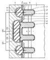
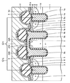
(実施の形態7)
図87は、本発明の実施の形態7における半導体装置のレイアウトを示す平面図である。図88は、図87のLXXXVIII−LXVIII線に沿った断面図であり、図89は、図87のLXXXIX−LXXXIX線に沿った断面図である。図90は、図88のXC−XC線に沿った不純物濃度分布である。なお、図87において斜線で示す部分は、p型不純物拡散領域41が形成されている領域である。また、図87においては、1つのゲート電極配線11aに沿って形成されたゲート用溝1a(図中点線)のみを示しているが、実際には、それぞれのゲート電極配線11aに沿って複数のゲート用溝1a(あるいはエミッタ用溝1b)が形成されている。図87〜図90を参照して、本実施の形態におけるIGBTの構成について説明する。
(Embodiment 7)
FIG. 87 is a plan view showing the layout of the semiconductor device according to the seventh embodiment of the present invention. 88 is a cross-sectional view taken along line LXXXVIII-LXVIII in FIG. 87, and FIG. 89 is a cross-sectional view taken along line LXXXIX-LXXXIX in FIG. FIG. 90 is an impurity concentration distribution along the XC-XC line of FIG. In FIG. 87, the hatched portion is a region where the p-type
特に図87を参照して、エミッタ電極11とゲート電極配線11aとは図中横方向に交互に配置されており、かつ図中縦方向に延在している。チップ中央部にあるゲート電極配線11aの図中下方端部には、他の配線と電気的に接続するためのゲートパッド28が設けられている。また、複数のゲート用溝1aの各々は、ゲート電極配線11aの真下において、ゲート電極配線11aの延在方向に沿って図中縦方向に配列している。複数のゲート用溝1aの各々は、その長方形の平面形状の短辺の延在方向(図中縦方向)に沿って配列している。図中縦方向で隣接するゲート用溝1a同士の間には、p型ボディ領域2およびn型不純物拡散領域14が形成されている。また、図中横方向で隣接するエミッタ電極11同士の間(すなわち、ゲート用溝1aの端部)には、p型不純物拡散領域41(ウェル層)が形成されている。p型不純物拡散領域41は、ゲート電極配線11aの真下において、エミッタ電極11に沿って図中縦方向に延在している。
Referring particularly to FIG. 87,
特に図88を参照して、n型不純物拡散領域14は、p型ボディ領域2とn-ドリフト層1との間に形成されている。n型不純物拡散領域14は、図90に示すように、n-ドリフト層1の不純物濃度よりも高い不純物濃度を有している。n型不純物拡散領域14が存在している場合、ゲート用溝1aおよびエミッタ用溝1b(たとえば図40)のうち少なくともいずれか一方を、n型不純物拡散領域14における不純物濃度が1×1016cm-3となる位置よりも第2主面側に突出させることで、高い耐圧(BVCES)を保持可能になる。図88に示す構成は、図39に示す構造Dの構成と実質的に同じである。
Referring specifically to FIG. 88, n type
特に図89を参照して、ゲート用溝1a内を埋め込むゲート電極5aは、ゲート用溝1a外部の第1主面上にも延びており、その延びた部分においてゲート電極配線11aと電気的に接続されている。ゲート電極配線11aの下層にはバリアメタル層10が位置し、バリアメタル層10とゲート電極5aとが接する領域にシリサイド層21aが形成されている。ゲート電極配線11aおよびエミッタ電極11上にパッシベーション膜15が形成されている。p型不純物拡散領域41は、ゲート用溝1aよりも深い位置に(第2主面側に)達している。
Referring in particular to FIG. 89,
なお、図87で示されている溝は全てゲート電極5aが埋め込まれたゲート用溝1aであるが、これらの溝のうち少なくとも1つがゲート用溝であればよく、その他の溝はたとえばエミッタ用溝であってもよい。
The grooves shown in FIG. 87 are all the
ここで、図88を参照して、ゲート用溝1aと隣接する他の溝(図では右側のゲート用溝1a)とのピッチをピッチXと規定する。また、半導体基板の第1主面からゲートトレンチを構成するゲート用溝1aの底部までの深さを深さYと規定する。また、p型ボディ領域2とn型不純物拡散領域14との接合面(n型不純物拡散領域14が形成されていない場合には、p型ボディ領域2とn-ドリフト層1との接合面)からのゲート用溝1aの突出量を突出量DTと規定する。さらに図89を参照して、p型不純物拡散領域41とn-ドリフト層1との接合面からゲート用溝1aの底部までの距離(深さ)を深さDT,Pwellと規定する。
Here, with reference to FIG. 88, the pitch between the
本願発明者は、トレンチ型ゲート構造のIGBTにおいて、ゲート用トレンチを以下の条件で設計することによって、IGBTの耐圧(降伏電圧)を向上できることを見出した。 The inventor of the present application has found that the breakdown voltage (breakdown voltage) of the IGBT can be improved by designing the gate trench under the following conditions in the IGBT having the trench type gate structure.
図91は、本発明の実施の形態7におけるY/XとBVCESとの関係を示す図である。図91を参照して、半導体基板の第1主面からゲートトレンチを構成するゲート用溝1aの底部までの深さYがゲート用溝1aと隣接する他の溝とのピッチよりも大きい場合(つまり1.0≦Y/Xの場合)には、高い降伏電圧BVCESが得られている。
FIG. 91 is a diagram showing a relationship between Y / X and BV CES in the seventh embodiment of the present invention. Referring to FIG. 91, when the depth Y from the first main surface of the semiconductor substrate to the bottom of
図92は、本発明の実施の形態7におけるDTとBVCESとの関係、およびDTとEP/CSまたはEP/N-との関係を示す図である。ここでEP/CSとは、p型ボディ領域2とn型不純物拡散領域14との接合面における電界強度を意味しており、EP/N-とは、n型不純物拡散領域14が形成されていない場合のp型ボディ領域2とn-ドリフト層1との接合面における電界強度を意味している。図92を参照して、p型ボディ領域2とn型不純物拡散領域14との接合面からのゲート用溝1aの突出量DTが1.0μm≦DTである場合には、電界強度EP/CSまたはEP/N-が低減されており、かつ高い降伏電圧BVCESが得られている。
FIG. 92 is a diagram showing a relationship between DT and BV CES and a relationship between DT and E P / CS or E P / N− in the seventh embodiment of the present invention. Here, E P / CS means the electric field strength at the junction surface between the p-
図93は、本発明の実施の形態7におけるDT,PwellとBVCESおよびΔBVCESとの関係を示す図である。ここでΔBVCESとは、ゲート電位を0V(エミッタ電位と同電位)とした場合のBVCESからゲート電位を−20Vとした場合のBVCESを引いた値を意味している。図93を参照して、ゲート用溝1aの底面からp型不純物拡散領域41の底面(p型不純物拡散領域41とn-ドリフト層1との接合面)までの深さDT,PwellがDT,Pwell≦1.0μmの場合には、高い降伏電圧BVCESが得られており、降伏電圧の変動量ΔBVCESも低く抑えられている。
FIG. 93 is a diagram showing a relationship between D T, Pwell , BV CES and ΔBV CES in the seventh embodiment of the present invention. Here, ΔBV CES means a value obtained by subtracting BV CES when the gate potential is −20 V from BV CES when the gate potential is 0 V (the same potential as the emitter potential). Referring to FIG. 93, the depths D T and Pwell from the bottom surface of
以上により、1.0≦Y/X、1.0μm≦DT、または0<DT,Pwell≦1.0μmの条件を満たすようにゲート用溝1a、エミッタ用溝1bを製造することによって、IGBTの耐圧を向上できる。
By manufacturing the
なお、図88においては、n型不純物拡散領域14がゲート用溝1a同士の間全体にわたって形成されている構成について説明したが、n型不純物拡散領域14は、以下の図94および図95に示すように、複数の溝同士の間の一部にのみ形成されていてもよい。
In FIG. 88, the configuration in which n-type
図94および図95は、本発明の実施の形態7におけるトレンチゲート型IGBTの各種の構成を示す概略断面図である。図94に示す構成においては、n型不純物拡散領域14がゲートトレンチの周囲にのみ形成されている。n型不純物拡散領域14は、ゲート用溝1aに接触し、かつエミッタ用溝1bに接触しないように形成されている。一方、図95に示す構成では、n型不純物拡散領域14がエミッタトレンチの周囲にのみ形成されている。n型不純物拡散領域14は、2つのエミッタ用溝1bの各々に接触し、かつゲート用溝1aに接触しないように形成されている。
94 and 95 are schematic cross-sectional views showing various configurations of the trench gate type IGBT according to the seventh embodiment of the present invention. In the configuration shown in FIG. 94, n-type
なお、これ以外の構成については、図40に示す構造Eの構成とほぼ同じであるため、同一の部材については同一の符号を付し、その説明を省略する。 In addition, since it is substantially the same as the structure of the structure E shown in FIG. 40 about another structure, the same code | symbol is attached | subjected about the same member and the description is abbreviate | omitted.
本願発明者は、n型不純物拡散領域14の幅およびエミッタ用溝1bからの距離を制御することによって、コレクタ・エミッタ間電圧を低減でき、破壊エネルギを向上できることを見出した。
The inventors of the present application have found that the collector-emitter voltage can be reduced and the breakdown energy can be improved by controlling the width of the n-type
図96は、WCSおよびXCSとVCEおよびESCとの関係を示す図である。ここで、WCSは平面的に見た場合の、エミッタ用溝1bの周囲に存在する領域におけるn型不純物拡散領域14の幅であり、XCSはエミッタ用溝1bからn型不純物拡散領域14の端部までの距離である。図96を参照して、n型不純物拡散領域14の幅WCSが6μm≦WCS≦9μmの場合、またはエミッタ用溝1bからn型不純物拡散領域14の端部までの距離XCSが0.5μm≦XCS≦2μmの場合には、コレクタ・エミッタ間電圧VCEが低減され、かつ高い短絡時の破壊エネルギESCが得られる。
FIG. 96 is a diagram showing the relationship between W CS and X CS and V CE and E SC . Here, W CS is the width of the n-type
図97は、本発明の実施の形態7における半導体装置におけるn型エミッタ領域3およびp+不純物拡散領域6の平面レイアウトを示す図である。図97を参照して、ゲート電極5aおよびエミッタ用導電層5bの各々が図中縦方向に延在しており、ゲート電極5aとエミッタ用導電層5bとの間、およびエミッタ用導電層5b同士の間にn型エミッタ領域3が形成されている。そして、n型エミッタ領域3は図中縦方向に延在しているおり、n型エミッタ領域3に挟まれた領域にp+不純物拡散領域6が周期的に形成されている。また、図98に示すように、n型エミッタ領域3とp+不純物拡散領域6とがゲート電極5aまたはエミッタ用導電層5bの延在方向(図中縦方向)に沿って交互に形成されていてもよい。
FIG. 97 shows a planar layout of n-
ここで、図97および図98に示すように、ゲート電極5aの延在方向に沿ったn型エミッタ領域3の幅をWSOと規定し、ゲート電極5aの延在方向に沿ったp+不純物拡散領域6の幅をWPCと規定する。本願発明者は、WSOとWPCとの関係を制御することによって、コレクタ・エミッタ間電圧を低減でき、破壊エネルギを向上できることを見出した。
Here, as shown in FIGS. 97 and 98, the width of n-
図99は、本発明の実施の形態7におけるαとVCE(sat)およびESCとの関係を示す図である。α(%)は、α=(WSO/WSO+WPC)×100で定義される値である。図99を参照して、αが8.0%≦α≦20.0%の範囲である場合には、低いコレクタ・エミッタ間電圧VCE(sat)が得られ、高い破壊エネルギESCが得られる。 FIG. 99 is a diagram showing the relationship between α, V CE (sat), and E SC in the seventh embodiment of the present invention. α (%) is a value defined by α = (W SO / W SO + W PC ) × 100. Referring to FIG. 99, when α is in the range of 8.0% ≦ α ≦ 20.0%, a low collector-emitter voltage V CE (sat) is obtained, and a high breakdown energy E SC is obtained. It is done.
(実施の形態8)
図100は、本発明の実施の形態8におけるゲートパッドの平面レイアウトを模式的に示す図である。図100を参照して、本実施の形態においては、ゲート電極配線11a(図87)の電流経路の一部が、局所的に高い抵抗を有する抵抗体28aによって形成されている。図100では、配線(表面ゲート配線)とゲート電極配線11aとを電気的に接続するためのゲートパッド28の一部が抵抗体28aによって形成されている。抵抗体28aの各々は、ゲートパッド28の中央部に設けられた開口部において、互いに対向するように突き出ている。抵抗体28aはたとえば図1または図75に示すゲート電極5aと同一の構造を有していてもよい。
(Embodiment 8)
FIG. 100 schematically shows a planar layout of the gate pad in the eighth embodiment of the present invention. Referring to FIG. 100, in the present embodiment, a part of the current path of
図101および図102は、ゲート電圧の発振現象を説明するための図である。トレンチゲート構造のIGBTやMOSトランジスタなどでは、スイッチング速度が速くなると、図101に示すような電流Icの変動時に、コレクタ・エミッタ間電圧VCEが発振する。この原因は、デバイスが発振してしまうようなLCR回路定数になることにある。そこで、抵抗体28aを設けることにより、デバイスが発振しにくいLCR回路定数となる。その結果、図102に示すように、ゲート電圧Vgeの発振現象を抑制することができる。
101 and 102 are diagrams for explaining the oscillation phenomenon of the gate voltage. In a trench gate IGBT or MOS transistor, when the switching speed increases, the collector-emitter voltage V CE oscillates when the current I c varies as shown in FIG. This is due to the LCR circuit constant that causes the device to oscillate. Therefore, by providing the
(実施の形態9)
IGBTにおけるVCE(sat)−EOFF特性を向上するためには、n-ドリフト層1の厚みを薄くすることが効果的であるが、n-ドリフト層1の厚みを薄くすると、高耐圧を実現することが難しくなる。そこで本願発明者は、p型ボディ領域2とn型不純物拡散領域14との接合面の電界強度EP/CS(n型不純物拡散領域14が形成されていない場合にはp型ボディ領域2とn-ドリフト層1との接合面の電界強度EP/N-)と、n型バッファ領域7とn-ドリフト層1との接合面の電界強度EN/N-との関係に着目することで、IGBTの耐圧を向上できることを見出した。
(Embodiment 9)
In order to improve the V CE (sat) -E OFF characteristics in the IGBT, n - although it is effective to reduce the thickness of the
図103は、本発明の実施の形態9におけるIGBTの主接合にブレークダウン電圧よりもわずかに低い逆バイアスを印加した時の図1のXIX−XIX線に沿った電界強度分布を模式的に示す図である。図104は、本発明の実施の形態9における接合面の電界強度と降伏電圧との関係を示す図である。 FIG. 103 schematically shows the electric field strength distribution along the XIX-XIX line in FIG. 1 when a reverse bias slightly lower than the breakdown voltage is applied to the main junction of the IGBT according to the ninth embodiment of the present invention. FIG. FIG. 104 is a diagram showing the relationship between the electric field strength at the junction surface and the breakdown voltage in the ninth embodiment of the present invention.
図103を参照して、IGBTの主接合にブレークダウン電圧よりもわずかに低い逆バイアスを印加した時の半導体内の電界は、半導体基板の第1主面からp型ボディ領域2とn-ドリフト層1との接合面までの領域において急激に増加し、その後、n-ドリフト層1内では緩やかに減少し、n-ドリフト層1とn型バッファ領域7において急激に減少している。また、p型ボディ領域2およびn型バッファ領域7内で電界が0となっている。図104を参照して、n-ドリフト層1とp型ボディ領域2との接合面の電界強度EP/N-が0<EP/N-≦3.0×1015(V/cm)の場合に、高い降伏電圧BVCESが得られる。また、n型バッファ領域7とn-ドリフト層1との接合面の電界強度EN/N-が2.0×1014≦EN/N-(V/cm)の場合に、高い降伏電圧BVCESが得られる。EN/N-はEP/N-以下であることが好ましい。
Referring to FIG. 103, the electric field in the semiconductor when a reverse bias slightly lower than the breakdown voltage is applied to the main junction of the IGBT, the p-
なお、実施の形態1〜8で説明した構造または数値範囲は、適宜組み合わせることができる。
Note that the structures or numerical ranges described in
以上に開示された実施の形態はすべての点で例示であって制限的なものではないと考慮されるべきである。本発明の範囲は、以上の実施の形態ではなく、特許請求の範囲によって示され、特許請求の範囲と均等の意味および範囲内でのすべての修正や変形を含むものと意図される。 The embodiment disclosed above should be considered as illustrative in all points and not restrictive. The scope of the present invention is shown not by the above embodiments but by the scope of claims, and is intended to include all modifications and variations within the scope and meaning equivalent to the scope of claims.
本発明は、並列的な動作に適した高耐圧半導体装置、特にIGBTを備える半導体装置として適している。 The present invention is suitable as a high voltage semiconductor device suitable for parallel operation, particularly as a semiconductor device including an IGBT.
1 n-ドリフト層、1a ゲート用溝、1b エミッタ用溝、2 p型ボディ領域、3 n型エミッタ領域またはn型不純物拡散領域、4,4a ゲート絶縁膜、4b エミッタ用絶縁膜、5 導電層、5a ゲート電極、5b エミッタ用導電層、6 p+不純物拡散領域、7 n型バッファ領域、7a n型中間層、8 p型コレクタ領域、9,22A,22B 絶縁膜、9a コンタクトホール、10 バリアメタル層、11 エミッタ電極、11a ゲート電極配線、12,12a コレクタ電極、14,14a n型不純物拡散領域、15 パッシベーション膜、21a,21b シリサイド層、28 ゲートパッド、28a 抵抗体、31 マスク層、32,33 シリコン酸化膜、32a 犠牲酸化膜、41 p型不純物拡散領域。
1 n - drift layer, 1a gate groove, 1b emitter groove, 2 p-type body region, 3 n-type emitter region or n-type impurity diffusion region, 4, 4a gate insulating film, 4b emitter insulating film, 5 a
Claims (1)
前記第1主面側に形成されたゲート電極(5a)と、前記第1主面側に形成された第1電極(11)と、前記第2主面に接触して形成された第2電極(12)とを有する素子とを備え、
前記素子は、前記ゲート電極に加えられる電圧によりチャネルに電界を発生させ、かつ前記チャネルの電界によって前記第1電極と前記第2電極との間の電流を制御し、
前記チャネルとなる第1導電型のボディ拡散層(2)と、
前記ボディ拡散層内に形成され、前記第1電極に接触する第2導電型のエミッタ拡散層(3)と、
前記第2主表面に形成され、第2導電型のドリフト拡散層(1)と第1導電型のコレクタ拡散層(8)とを含み、前記第2電極に電気的に接続されるコレクタ領域と、
前記ボディ拡散層と前記ドリフト拡散層との間に形成された第2導電型の埋込拡散層(14)と
を備え、
前記半導体基板の前記第1主面にはゲート用溝(1a)が形成されており、前記ゲート用溝(1a)内には前記ゲート電極(5a)が埋め込まれており、
前記半導体基板の前記第1主面には複数の溝(1a、1b)が形成されており、かつ前記複数の溝の各々は平面的に見て一の方向に配列しており、かつ前記ゲート用溝(1a)は前記複数の溝のうち少なくとも1つであり、
前記複数の溝の各々に隣接して前記第1の主面に形成され、かつ平面的に見て前記一の方向に延在し、かつ前記複数の溝の各々よりも深く形成された第1導電型のウェル層(41)をさらに備え、
前記半導体基板の厚さは50〜800μmであり、
前記ボディ拡散層の不純物濃度は1×1015cm−3〜1×1018cm−3、前記ボディ拡散層の前記第1主表面からの拡散深さは1.0μm〜4.0μmであり、
前記エミッタ拡散層の不純物濃度は1×1018cm−3〜1×1020cm−3、前記エミッタ拡散層の前記第1主表面からの拡散深さは0.3μm〜2.0μmであり、
前記ドリフト拡散層の不純物濃度は1×1012cm−3〜1×1015cm−3 であり、
前記埋込拡散層の不純物濃度は、前記ドリフト拡散層の不純物濃度よりも高い不純物濃度であり、
前記ゲート用溝の深さは3μm〜10μmであり、
前記溝は、前記埋込拡散層における不純物濃度が1×1016cm−3となる位置よりも前記第2主表面側に突出しており、
前記ゲート用溝の底面から前記ウェル層の底部までの深さ(DT,Pwell)は、0よりも
大きく1.0μm以下である、半導体装置。 A semiconductor substrate having a first main surface and a second main surface facing each other;
A gate electrode (5a) formed on the first main surface side, a first electrode (11) formed on the first main surface side, and a second electrode formed in contact with the second main surface And (12) an element having
The element generates an electric field in a channel by a voltage applied to the gate electrode, and controls a current between the first electrode and the second electrode by the electric field of the channel,
A first diffusion type body diffusion layer (2) serving as the channel;
A second conductivity type emitter diffusion layer (3) formed in the body diffusion layer and in contact with the first electrode;
A collector region formed on the second main surface, including a second conductivity type drift diffusion layer (1) and a first conductivity type collector diffusion layer (8), and electrically connected to the second electrode; ,
A second conductivity type buried diffusion layer (14) formed between the body diffusion layer and the drift diffusion layer;
A gate groove (1a) is formed in the first main surface of the semiconductor substrate, and the gate electrode (5a) is embedded in the gate groove (1a),
A plurality of grooves (1a, 1b) are formed in the first main surface of the semiconductor substrate, and each of the plurality of grooves is arranged in one direction as viewed in plan, and the gate The groove (1a) is at least one of the plurality of grooves,
First formed on the first main surface adjacent to each of the plurality of grooves, extending in the one direction as viewed in plan, and deeper than each of the plurality of grooves. A conductive well layer (41);
The thickness of the semiconductor substrate is 50~800Myuemu,
The body impurity concentration of the diffusion layer is 1 × 10 15 cm -3 ~1 × 10 18 cm -3, the diffusion depth from the first major surface of the body diffusion layer is 1.0Myuemu~4.0Myuemu,
It said emitter impurity concentration of the diffusion layer is 1 × 10 18 cm -3 ~1 × 10 20 cm -3, the diffusion depth from the first major surface of the emitter diffusion layer is 0.3Myuemu~2.0Myuemu,
The impurity concentration of the drift diffusion layer is 1 × 10 12 cm -3 ~1 × 10 15 cm -3,
The impurity concentration of the buried diffusion layer is a high impurity concentration than the impurity concentration of the drift diffusion layer,
The depth of the gate groove is 3Myuemu~10myuemu,
Said groove protrudes to the second main surface side of a position where the impurity concentration of the buried diffusion layer is 1 × 10 16 cm -3,
A depth (DT, Pwell) from the bottom of the gate groove to the bottom of the well layer is greater than 0 and equal to or less than 1.0 μm.
Priority Applications (1)
| Application Number | Priority Date | Filing Date | Title |
|---|---|---|---|
| JP2014087359A JP5908524B2 (en) | 2014-04-21 | 2014-04-21 | Semiconductor device |
Applications Claiming Priority (1)
| Application Number | Priority Date | Filing Date | Title |
|---|---|---|---|
| JP2014087359A JP5908524B2 (en) | 2014-04-21 | 2014-04-21 | Semiconductor device |
Related Parent Applications (1)
| Application Number | Title | Priority Date | Filing Date |
|---|---|---|---|
| JP2010505147A Division JPWO2009122486A1 (en) | 2008-03-31 | 2008-03-31 | Semiconductor device |
Related Child Applications (1)
| Application Number | Title | Priority Date | Filing Date |
|---|---|---|---|
| JP2016058154A Division JP6280148B2 (en) | 2016-03-23 | 2016-03-23 | Semiconductor device |
Publications (2)
| Publication Number | Publication Date |
|---|---|
| JP2014158041A JP2014158041A (en) | 2014-08-28 |
| JP5908524B2 true JP5908524B2 (en) | 2016-04-26 |
Family
ID=51578693
Family Applications (1)
| Application Number | Title | Priority Date | Filing Date |
|---|---|---|---|
| JP2014087359A Active JP5908524B2 (en) | 2014-04-21 | 2014-04-21 | Semiconductor device |
Country Status (1)
| Country | Link |
|---|---|
| JP (1) | JP5908524B2 (en) |
Cited By (2)
| Publication number | Priority date | Publication date | Assignee | Title |
|---|---|---|---|---|
| US10026803B1 (en) | 2016-12-27 | 2018-07-17 | Mitsubishi Electric Corporation | Semiconductor device, power conversion device, and method of manufacturing semiconductor device |
| US11101133B2 (en) | 2018-08-17 | 2021-08-24 | Mitsubishi Electric Corporation | Semiconductor device and manufacturing method thereof |
Families Citing this family (6)
| Publication number | Priority date | Publication date | Assignee | Title |
|---|---|---|---|---|
| WO2016051970A1 (en) * | 2014-09-30 | 2016-04-07 | 富士電機株式会社 | Semiconductor device and semiconductor device manufacturing method |
| WO2017006711A1 (en) | 2015-07-07 | 2017-01-12 | 富士電機株式会社 | Semiconductor device |
| DE112016000210T5 (en) | 2015-07-16 | 2017-09-07 | Fuji Electric Co., Ltd. | Semiconductor device and method for manufacturing the semiconductor device |
| JP6832645B2 (en) * | 2016-07-20 | 2021-02-24 | ローム株式会社 | Semiconductor device |
| CN106783988A (en) * | 2017-01-05 | 2017-05-31 | 江苏中科君芯科技有限公司 | IGBT device with anti-short circuit capability high |
| CN110574153B (en) * | 2017-11-13 | 2024-02-23 | 富士电机株式会社 | Semiconductor device and method for manufacturing semiconductor device |
Family Cites Families (2)
| Publication number | Priority date | Publication date | Assignee | Title |
|---|---|---|---|---|
| JP3976374B2 (en) * | 1997-07-11 | 2007-09-19 | 三菱電機株式会社 | Semiconductor device having trench MOS gate structure and manufacturing method thereof |
| WO2002061845A1 (en) * | 2001-02-01 | 2002-08-08 | Mitsubishi Denki Kabushiki Kaisha | Semiconductor device and method of manufacturing the same |
-
2014
- 2014-04-21 JP JP2014087359A patent/JP5908524B2/en active Active
Cited By (2)
| Publication number | Priority date | Publication date | Assignee | Title |
|---|---|---|---|---|
| US10026803B1 (en) | 2016-12-27 | 2018-07-17 | Mitsubishi Electric Corporation | Semiconductor device, power conversion device, and method of manufacturing semiconductor device |
| US11101133B2 (en) | 2018-08-17 | 2021-08-24 | Mitsubishi Electric Corporation | Semiconductor device and manufacturing method thereof |
Also Published As
| Publication number | Publication date |
|---|---|
| JP2014158041A (en) | 2014-08-28 |
Similar Documents
| Publication | Publication Date | Title |
|---|---|---|
| KR101191281B1 (en) | Semiconductor device | |
| JP5908524B2 (en) | Semiconductor device | |
| US10269946B2 (en) | Semiconductor device and method of manufacturing the same | |
| JP5025071B2 (en) | Semiconductor device and manufacturing method thereof | |
| US9614106B2 (en) | Semiconductor device | |
| JP5605073B2 (en) | Semiconductor device | |
| JP5384878B2 (en) | Semiconductor device and manufacturing method thereof | |
| JP6289683B2 (en) | Semiconductor device | |
| US10068999B2 (en) | Vertical power component | |
| JP6089818B2 (en) | Semiconductor device and manufacturing method thereof | |
| WO2017130374A1 (en) | Power semiconductor device and method for manufacturing power semiconductor device | |
| JP6280148B2 (en) | Semiconductor device | |
| US20150144989A1 (en) | Power semiconductor device and method of manufacturing the same | |
| JP2011176026A (en) | Method of manufacturing semiconductor element | |
| JP6513168B2 (en) | Semiconductor device | |
| JP6026767B2 (en) | Semiconductor device and manufacturing method thereof | |
| TW201232781A (en) | Semiconductor device and method for manufacturing same | |
| WO2016001182A2 (en) | Semiconductor device | |
| JP2019057674A (en) | Semiconductor device | |
| CN111295765A (en) | Semiconductor device with a plurality of semiconductor chips | |
| JP2004266298A (en) | Vertical semiconductor device | |
| KR20150056433A (en) | Power semiconductor device and method of manufacturing the same | |
| JP2010147366A (en) | Semiconductor device |
Legal Events
| Date | Code | Title | Description |
|---|---|---|---|
| A977 | Report on retrieval |
Free format text: JAPANESE INTERMEDIATE CODE: A971007 Effective date: 20150319 |
|
| A131 | Notification of reasons for refusal |
Free format text: JAPANESE INTERMEDIATE CODE: A131 Effective date: 20150324 |
|
| A521 | Request for written amendment filed |
Free format text: JAPANESE INTERMEDIATE CODE: A523 Effective date: 20150430 |
|
| A131 | Notification of reasons for refusal |
Free format text: JAPANESE INTERMEDIATE CODE: A131 Effective date: 20150602 |
|
| A521 | Request for written amendment filed |
Free format text: JAPANESE INTERMEDIATE CODE: A523 Effective date: 20150624 |
|
| TRDD | Decision of grant or rejection written | ||
| A01 | Written decision to grant a patent or to grant a registration (utility model) |
Free format text: JAPANESE INTERMEDIATE CODE: A01 Effective date: 20160223 |
|
| A61 | First payment of annual fees (during grant procedure) |
Free format text: JAPANESE INTERMEDIATE CODE: A61 Effective date: 20160323 |
|
| R150 | Certificate of patent or registration of utility model |
Ref document number: 5908524 Country of ref document: JP Free format text: JAPANESE INTERMEDIATE CODE: R150 |
|
| R250 | Receipt of annual fees |
Free format text: JAPANESE INTERMEDIATE CODE: R250 |
|
| R250 | Receipt of annual fees |
Free format text: JAPANESE INTERMEDIATE CODE: R250 |
|
| R250 | Receipt of annual fees |
Free format text: JAPANESE INTERMEDIATE CODE: R250 |
|
| R250 | Receipt of annual fees |
Free format text: JAPANESE INTERMEDIATE CODE: R250 |
|
| R250 | Receipt of annual fees |
Free format text: JAPANESE INTERMEDIATE CODE: R250 |
|
| R250 | Receipt of annual fees |
Free format text: JAPANESE INTERMEDIATE CODE: R250 |