JP5838832B2 - 基板集合体、電子デバイス、及び基板集合体の製造方法 - Google Patents
基板集合体、電子デバイス、及び基板集合体の製造方法 Download PDFInfo
- Publication number
- JP5838832B2 JP5838832B2 JP2012016387A JP2012016387A JP5838832B2 JP 5838832 B2 JP5838832 B2 JP 5838832B2 JP 2012016387 A JP2012016387 A JP 2012016387A JP 2012016387 A JP2012016387 A JP 2012016387A JP 5838832 B2 JP5838832 B2 JP 5838832B2
- Authority
- JP
- Japan
- Prior art keywords
- groove
- substrate
- substrate assembly
- assembly
- grooves
- Prior art date
- Legal status (The legal status is an assumption and is not a legal conclusion. Google has not performed a legal analysis and makes no representation as to the accuracy of the status listed.)
- Expired - Fee Related
Links
- 239000000758 substrate Substances 0.000 title claims description 211
- 238000004519 manufacturing process Methods 0.000 title claims description 18
- 239000000463 material Substances 0.000 claims description 19
- 238000005245 sintering Methods 0.000 claims description 11
- 239000002994 raw material Substances 0.000 claims description 9
- 238000003825 pressing Methods 0.000 claims description 6
- 238000000034 method Methods 0.000 description 21
- 230000002093 peripheral effect Effects 0.000 description 15
- 239000000919 ceramic Substances 0.000 description 6
- 239000010453 quartz Substances 0.000 description 6
- VYPSYNLAJGMNEJ-UHFFFAOYSA-N silicon dioxide Inorganic materials O=[Si]=O VYPSYNLAJGMNEJ-UHFFFAOYSA-N 0.000 description 6
- 230000000712 assembly Effects 0.000 description 5
- 238000000429 assembly Methods 0.000 description 5
- 239000012141 concentrate Substances 0.000 description 5
- 238000005520 cutting process Methods 0.000 description 3
- 238000005530 etching Methods 0.000 description 3
- 239000011521 glass Substances 0.000 description 3
- 230000001678 irradiating effect Effects 0.000 description 3
- KRHYYFGTRYWZRS-UHFFFAOYSA-N Fluorane Chemical compound F KRHYYFGTRYWZRS-UHFFFAOYSA-N 0.000 description 2
- 239000000853 adhesive Substances 0.000 description 2
- 230000001070 adhesive effect Effects 0.000 description 2
- 239000011159 matrix material Substances 0.000 description 2
- 230000000149 penetrating effect Effects 0.000 description 2
- 238000005488 sandblasting Methods 0.000 description 2
- 238000007789 sealing Methods 0.000 description 2
- 230000004308 accommodation Effects 0.000 description 1
- 230000015572 biosynthetic process Effects 0.000 description 1
- 230000007547 defect Effects 0.000 description 1
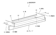
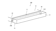
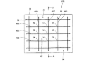
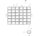
- 238000010586 diagram Methods 0.000 description 1
- 230000000694 effects Effects 0.000 description 1
- 238000005516 engineering process Methods 0.000 description 1
- 239000012634 fragment Substances 0.000 description 1
- 239000012212 insulator Substances 0.000 description 1
- 238000005304 joining Methods 0.000 description 1
Images


Landscapes
- Structure Of Printed Boards (AREA)
Priority Applications (1)
| Application Number | Priority Date | Filing Date | Title |
|---|---|---|---|
| JP2012016387A JP5838832B2 (ja) | 2012-01-30 | 2012-01-30 | 基板集合体、電子デバイス、及び基板集合体の製造方法 |
Applications Claiming Priority (1)
| Application Number | Priority Date | Filing Date | Title |
|---|---|---|---|
| JP2012016387A JP5838832B2 (ja) | 2012-01-30 | 2012-01-30 | 基板集合体、電子デバイス、及び基板集合体の製造方法 |
Publications (3)
| Publication Number | Publication Date |
|---|---|
| JP2013157432A JP2013157432A (ja) | 2013-08-15 |
| JP2013157432A5 JP2013157432A5 (https=) | 2015-02-26 |
| JP5838832B2 true JP5838832B2 (ja) | 2016-01-06 |
Family
ID=49052340
Family Applications (1)
| Application Number | Title | Priority Date | Filing Date |
|---|---|---|---|
| JP2012016387A Expired - Fee Related JP5838832B2 (ja) | 2012-01-30 | 2012-01-30 | 基板集合体、電子デバイス、及び基板集合体の製造方法 |
Country Status (1)
| Country | Link |
|---|---|
| JP (1) | JP5838832B2 (https=) |
Families Citing this family (1)
| Publication number | Priority date | Publication date | Assignee | Title |
|---|---|---|---|---|
| JP2017195318A (ja) * | 2016-04-22 | 2017-10-26 | 株式会社明電舎 | 集合基板 |
Family Cites Families (13)
| Publication number | Priority date | Publication date | Assignee | Title |
|---|---|---|---|---|
| JPH01100989A (ja) * | 1987-10-14 | 1989-04-19 | Matsushita Electric Ind Co Ltd | セラミック基板の構造 |
| JPH0249162U (https=) * | 1988-09-30 | 1990-04-05 | ||
| JPH0275765U (https=) * | 1988-11-29 | 1990-06-11 | ||
| JPH03252191A (ja) * | 1990-03-01 | 1991-11-11 | Matsushita Electric Ind Co Ltd | 金属基材絶縁基板 |
| JPH05226794A (ja) * | 1992-02-17 | 1993-09-03 | Horiba Ltd | プリント配線基板およびプリント配線基板用母材 |
| JP2566288Y2 (ja) * | 1992-02-21 | 1998-03-25 | 昭和電工株式会社 | 回路用基板 |
| JP3878871B2 (ja) * | 2002-03-19 | 2007-02-07 | 京セラ株式会社 | 多数個取りセラミック基板 |
| JP2003304038A (ja) * | 2002-04-11 | 2003-10-24 | Fuji Photo Film Co Ltd | 配線基板 |
| JP2004221514A (ja) * | 2002-11-22 | 2004-08-05 | Kyocera Corp | 多数個取り配線基板 |
| JP2005340541A (ja) * | 2004-05-27 | 2005-12-08 | Kyocera Corp | 多数個取り配線基板 |
| JP2006270083A (ja) * | 2005-02-25 | 2006-10-05 | Kyocera Corp | 集合基板及びその製造方法 |
| JP2007318035A (ja) * | 2006-05-29 | 2007-12-06 | Kyocera Corp | 多数個取り配線基板、電子部品収納用パッケージおよび電子装置 |
| JP5052398B2 (ja) * | 2008-04-24 | 2012-10-17 | 京セラ株式会社 | 多数個取り配線基板および配線基板ならびに電子装置 |
-
2012
- 2012-01-30 JP JP2012016387A patent/JP5838832B2/ja not_active Expired - Fee Related
Also Published As
| Publication number | Publication date |
|---|---|
| JP2013157432A (ja) | 2013-08-15 |
Similar Documents
| Publication | Publication Date | Title |
|---|---|---|
| JP4324811B2 (ja) | 圧電振動子及びその製造方法 | |
| JP5276035B2 (ja) | 圧電デバイスの製造方法及び圧電デバイス | |
| WO2014174945A1 (ja) | 水晶振動装置 | |
| JP4407845B2 (ja) | 圧電振動子及びその製造方法並びに圧電振動子用の蓋 | |
| CN109155620B (zh) | 压电振动器件及压电振动器件的制造方法 | |
| JP5213614B2 (ja) | 圧電デバイスおよびその製造方法 | |
| US8429800B2 (en) | Methods for manufacturing piezoelectric vibrating pieces | |
| JP2018074267A (ja) | 圧電振動片及び圧電デバイス | |
| JP6233392B2 (ja) | 水晶振動装置及びその製造方法 | |
| JP5838832B2 (ja) | 基板集合体、電子デバイス、及び基板集合体の製造方法 | |
| JP2011229114A (ja) | 圧電デバイス及びその製造方法 | |
| US10938368B2 (en) | Piezoelectric-resonator-mounting substrate, and piezoelectric resonator unit and method of manufacturing the piezoelectric resonator unit | |
| JP6288260B2 (ja) | 脆性基板の分断方法 | |
| JP2012186729A (ja) | ウエハおよびパッケージ製品の製造方法 | |
| JP2011124881A (ja) | 水晶振動子、電子部品および水晶振動子の製造方法 | |
| JP5975178B2 (ja) | 超音波発生素子、超音波発生装置及び超音波発生素子の製造方法 | |
| JP2013120762A (ja) | 蓋体、パッケージ、電子部品及びパッケージの製造方法 | |
| JP6888635B2 (ja) | 水晶振動板ウエハとその水晶振動板 | |
| JP6645211B2 (ja) | 水晶振動デバイスの製造方法 | |
| JPWO2022130670A5 (https=) | ||
| JP2015139012A (ja) | 水晶振動子及びその製造方法 | |
| CN111052351B (zh) | 电子部件 | |
| JP2012195918A (ja) | 圧電デバイス | |
| JP2015154036A (ja) | 個片素子の実装方法及び半導体装置 | |
| CN203206188U (zh) | 压电振动装置 |
Legal Events
| Date | Code | Title | Description |
|---|---|---|---|
| A521 | Request for written amendment filed |
Free format text: JAPANESE INTERMEDIATE CODE: A523 Effective date: 20150106 |
|
| A621 | Written request for application examination |
Free format text: JAPANESE INTERMEDIATE CODE: A621 Effective date: 20150106 |
|
| RD04 | Notification of resignation of power of attorney |
Free format text: JAPANESE INTERMEDIATE CODE: A7424 Effective date: 20150107 |
|
| A977 | Report on retrieval |
Free format text: JAPANESE INTERMEDIATE CODE: A971007 Effective date: 20150731 |
|
| A131 | Notification of reasons for refusal |
Free format text: JAPANESE INTERMEDIATE CODE: A131 Effective date: 20150804 |
|
| A521 | Request for written amendment filed |
Free format text: JAPANESE INTERMEDIATE CODE: A523 Effective date: 20150908 |
|
| TRDD | Decision of grant or rejection written | ||
| A01 | Written decision to grant a patent or to grant a registration (utility model) |
Free format text: JAPANESE INTERMEDIATE CODE: A01 Effective date: 20151013 |
|
| A61 | First payment of annual fees (during grant procedure) |
Free format text: JAPANESE INTERMEDIATE CODE: A61 Effective date: 20151026 |
|
| R150 | Certificate of patent or registration of utility model |
Ref document number: 5838832 Country of ref document: JP Free format text: JAPANESE INTERMEDIATE CODE: R150 |
|
| S531 | Written request for registration of change of domicile |
Free format text: JAPANESE INTERMEDIATE CODE: R313531 |
|
| R350 | Written notification of registration of transfer |
Free format text: JAPANESE INTERMEDIATE CODE: R350 |
|
| LAPS | Cancellation because of no payment of annual fees |