JP5809866B2 - 光素子モジュール、光伝送モジュール、および光伝送モジュールの製造方法 - Google Patents
光素子モジュール、光伝送モジュール、および光伝送モジュールの製造方法 Download PDFInfo
- Publication number
- JP5809866B2 JP5809866B2 JP2011159847A JP2011159847A JP5809866B2 JP 5809866 B2 JP5809866 B2 JP 5809866B2 JP 2011159847 A JP2011159847 A JP 2011159847A JP 2011159847 A JP2011159847 A JP 2011159847A JP 5809866 B2 JP5809866 B2 JP 5809866B2
- Authority
- JP
- Japan
- Prior art keywords
- optical
- optical element
- hole
- substrate
- optical fiber
- Prior art date
- Legal status (The legal status is an assumption and is not a legal conclusion. Google has not performed a legal analysis and makes no representation as to the accuracy of the status listed.)
- Active
Links
- 230000003287 optical effect Effects 0.000 title claims description 229
- 230000005540 biological transmission Effects 0.000 title claims description 82
- 238000004519 manufacturing process Methods 0.000 title claims description 14
- 239000013307 optical fiber Substances 0.000 claims description 107
- 239000000758 substrate Substances 0.000 claims description 96
- 239000000853 adhesive Substances 0.000 claims description 44
- 230000001070 adhesive effect Effects 0.000 claims description 42
- 238000003780 insertion Methods 0.000 claims description 14
- 230000037431 insertion Effects 0.000 claims description 14
- 238000000034 method Methods 0.000 claims description 6
- 238000005304 joining Methods 0.000 claims description 3
- 239000002023 wood Substances 0.000 claims 1
- 238000012986 modification Methods 0.000 description 20
- 230000004048 modification Effects 0.000 description 20
- 229910000679 solder Inorganic materials 0.000 description 6
- 238000004891 communication Methods 0.000 description 5
- 238000003384 imaging method Methods 0.000 description 5
- 238000012545 processing Methods 0.000 description 5
- 238000006243 chemical reaction Methods 0.000 description 4
- 239000011521 glass Substances 0.000 description 3
- 239000000463 material Substances 0.000 description 3
- 239000000919 ceramic Substances 0.000 description 2
- 239000003795 chemical substances by application Substances 0.000 description 2
- 238000013461 design Methods 0.000 description 2
- 230000002542 deteriorative effect Effects 0.000 description 2
- 230000000694 effects Effects 0.000 description 2
- 239000011347 resin Substances 0.000 description 2
- 229920005989 resin Polymers 0.000 description 2
- 230000008054 signal transmission Effects 0.000 description 2
- 239000004593 Epoxy Substances 0.000 description 1
- 230000003321 amplification Effects 0.000 description 1
- 238000005253 cladding Methods 0.000 description 1
- 230000008878 coupling Effects 0.000 description 1
- 238000010168 coupling process Methods 0.000 description 1
- 238000005859 coupling reaction Methods 0.000 description 1
- 239000000835 fiber Substances 0.000 description 1
- 238000007689 inspection Methods 0.000 description 1
- 230000003902 lesion Effects 0.000 description 1
- 238000002844 melting Methods 0.000 description 1
- 230000008018 melting Effects 0.000 description 1
- 239000002184 metal Substances 0.000 description 1
- 238000003199 nucleic acid amplification method Methods 0.000 description 1
- 230000002093 peripheral effect Effects 0.000 description 1
- 238000000206 photolithography Methods 0.000 description 1
- 230000000007 visual effect Effects 0.000 description 1
Images


Classifications
-
- H—ELECTRICITY
- H01—ELECTRIC ELEMENTS
- H01L—SEMICONDUCTOR DEVICES NOT COVERED BY CLASS H10
- H01L31/00—Semiconductor devices sensitive to infrared radiation, light, electromagnetic radiation of shorter wavelength or corpuscular radiation and specially adapted either for the conversion of the energy of such radiation into electrical energy or for the control of electrical energy by such radiation; Processes or apparatus specially adapted for the manufacture or treatment thereof or of parts thereof; Details thereof
- H01L31/02—Details
- H01L31/0232—Optical elements or arrangements associated with the device
- H01L31/02325—Optical elements or arrangements associated with the device the optical elements not being integrated nor being directly associated with the device
-
- H—ELECTRICITY
- H01—ELECTRIC ELEMENTS
- H01S—DEVICES USING THE PROCESS OF LIGHT AMPLIFICATION BY STIMULATED EMISSION OF RADIATION [LASER] TO AMPLIFY OR GENERATE LIGHT; DEVICES USING STIMULATED EMISSION OF ELECTROMAGNETIC RADIATION IN WAVE RANGES OTHER THAN OPTICAL
- H01S5/00—Semiconductor lasers
- H01S5/02—Structural details or components not essential to laser action
- H01S5/022—Mountings; Housings
- H01S5/023—Mount members, e.g. sub-mount members
- H01S5/02325—Mechanically integrated components on mount members or optical micro-benches
- H01S5/02326—Arrangements for relative positioning of laser diodes and optical components, e.g. grooves in the mount to fix optical fibres or lenses
-
- A—HUMAN NECESSITIES
- A61—MEDICAL OR VETERINARY SCIENCE; HYGIENE
- A61B—DIAGNOSIS; SURGERY; IDENTIFICATION
- A61B1/00—Instruments for performing medical examinations of the interior of cavities or tubes of the body by visual or photographical inspection, e.g. endoscopes; Illuminating arrangements therefor
- A61B1/00002—Operational features of endoscopes
- A61B1/00011—Operational features of endoscopes characterised by signal transmission
- A61B1/00013—Operational features of endoscopes characterised by signal transmission using optical means
-
- G—PHYSICS
- G02—OPTICS
- G02B—OPTICAL ELEMENTS, SYSTEMS OR APPARATUS
- G02B6/00—Light guides; Structural details of arrangements comprising light guides and other optical elements, e.g. couplings
- G02B6/24—Coupling light guides
- G02B6/36—Mechanical coupling means
- G02B6/3628—Mechanical coupling means for mounting fibres to supporting carriers
- G02B6/3632—Mechanical coupling means for mounting fibres to supporting carriers characterised by the cross-sectional shape of the mechanical coupling means
- G02B6/3644—Mechanical coupling means for mounting fibres to supporting carriers characterised by the cross-sectional shape of the mechanical coupling means the coupling means being through-holes or wall apertures
-
- G—PHYSICS
- G02—OPTICS
- G02B—OPTICAL ELEMENTS, SYSTEMS OR APPARATUS
- G02B6/00—Light guides; Structural details of arrangements comprising light guides and other optical elements, e.g. couplings
- G02B6/24—Coupling light guides
- G02B6/42—Coupling light guides with opto-electronic elements
- G02B6/4201—Packages, e.g. shape, construction, internal or external details
- G02B6/4202—Packages, e.g. shape, construction, internal or external details for coupling an active element with fibres without intermediate optical elements, e.g. fibres with plane ends, fibres with shaped ends, bundles
-
- G—PHYSICS
- G02—OPTICS
- G02B—OPTICAL ELEMENTS, SYSTEMS OR APPARATUS
- G02B6/00—Light guides; Structural details of arrangements comprising light guides and other optical elements, e.g. couplings
- G02B6/24—Coupling light guides
- G02B6/42—Coupling light guides with opto-electronic elements
- G02B6/4201—Packages, e.g. shape, construction, internal or external details
- G02B6/4256—Details of housings
- G02B6/4257—Details of housings having a supporting carrier or a mounting substrate or a mounting plate
-
- H—ELECTRICITY
- H01—ELECTRIC ELEMENTS
- H01L—SEMICONDUCTOR DEVICES NOT COVERED BY CLASS H10
- H01L33/00—Semiconductor devices with at least one potential-jump barrier or surface barrier specially adapted for light emission; Processes or apparatus specially adapted for the manufacture or treatment thereof or of parts thereof; Details thereof
- H01L33/48—Semiconductor devices with at least one potential-jump barrier or surface barrier specially adapted for light emission; Processes or apparatus specially adapted for the manufacture or treatment thereof or of parts thereof; Details thereof characterised by the semiconductor body packages
- H01L33/58—Optical field-shaping elements
-
- G—PHYSICS
- G02—OPTICS
- G02B—OPTICAL ELEMENTS, SYSTEMS OR APPARATUS
- G02B6/00—Light guides; Structural details of arrangements comprising light guides and other optical elements, e.g. couplings
- G02B6/24—Coupling light guides
- G02B6/42—Coupling light guides with opto-electronic elements
- G02B6/4201—Packages, e.g. shape, construction, internal or external details
- G02B6/4219—Mechanical fixtures for holding or positioning the elements relative to each other in the couplings; Alignment methods for the elements, e.g. measuring or observing methods especially used therefor
- G02B6/4236—Fixing or mounting methods of the aligned elements
- G02B6/4239—Adhesive bonding; Encapsulation with polymer material
-
- H—ELECTRICITY
- H01—ELECTRIC ELEMENTS
- H01L—SEMICONDUCTOR DEVICES NOT COVERED BY CLASS H10
- H01L2224/00—Indexing scheme for arrangements for connecting or disconnecting semiconductor or solid-state bodies and methods related thereto as covered by H01L24/00
- H01L2224/01—Means for bonding being attached to, or being formed on, the surface to be connected, e.g. chip-to-package, die-attach, "first-level" interconnects; Manufacturing methods related thereto
- H01L2224/10—Bump connectors; Manufacturing methods related thereto
- H01L2224/12—Structure, shape, material or disposition of the bump connectors prior to the connecting process
- H01L2224/13—Structure, shape, material or disposition of the bump connectors prior to the connecting process of an individual bump connector
-
- H—ELECTRICITY
- H01—ELECTRIC ELEMENTS
- H01L—SEMICONDUCTOR DEVICES NOT COVERED BY CLASS H10
- H01L2224/00—Indexing scheme for arrangements for connecting or disconnecting semiconductor or solid-state bodies and methods related thereto as covered by H01L24/00
- H01L2224/01—Means for bonding being attached to, or being formed on, the surface to be connected, e.g. chip-to-package, die-attach, "first-level" interconnects; Manufacturing methods related thereto
- H01L2224/42—Wire connectors; Manufacturing methods related thereto
- H01L2224/44—Structure, shape, material or disposition of the wire connectors prior to the connecting process
- H01L2224/45—Structure, shape, material or disposition of the wire connectors prior to the connecting process of an individual wire connector
- H01L2224/45001—Core members of the connector
- H01L2224/45099—Material
- H01L2224/451—Material with a principal constituent of the material being a metal or a metalloid, e.g. boron (B), silicon (Si), germanium (Ge), arsenic (As), antimony (Sb), tellurium (Te) and polonium (Po), and alloys thereof
- H01L2224/45138—Material with a principal constituent of the material being a metal or a metalloid, e.g. boron (B), silicon (Si), germanium (Ge), arsenic (As), antimony (Sb), tellurium (Te) and polonium (Po), and alloys thereof the principal constituent melting at a temperature of greater than or equal to 950°C and less than 1550°C
- H01L2224/45144—Gold (Au) as principal constituent
-
- H—ELECTRICITY
- H01—ELECTRIC ELEMENTS
- H01L—SEMICONDUCTOR DEVICES NOT COVERED BY CLASS H10
- H01L2224/00—Indexing scheme for arrangements for connecting or disconnecting semiconductor or solid-state bodies and methods related thereto as covered by H01L24/00
- H01L2224/01—Means for bonding being attached to, or being formed on, the surface to be connected, e.g. chip-to-package, die-attach, "first-level" interconnects; Manufacturing methods related thereto
- H01L2224/42—Wire connectors; Manufacturing methods related thereto
- H01L2224/47—Structure, shape, material or disposition of the wire connectors after the connecting process
- H01L2224/48—Structure, shape, material or disposition of the wire connectors after the connecting process of an individual wire connector
- H01L2224/4805—Shape
- H01L2224/4809—Loop shape
- H01L2224/48091—Arched
-
- H—ELECTRICITY
- H01—ELECTRIC ELEMENTS
- H01L—SEMICONDUCTOR DEVICES NOT COVERED BY CLASS H10
- H01L2224/00—Indexing scheme for arrangements for connecting or disconnecting semiconductor or solid-state bodies and methods related thereto as covered by H01L24/00
- H01L2224/01—Means for bonding being attached to, or being formed on, the surface to be connected, e.g. chip-to-package, die-attach, "first-level" interconnects; Manufacturing methods related thereto
- H01L2224/42—Wire connectors; Manufacturing methods related thereto
- H01L2224/47—Structure, shape, material or disposition of the wire connectors after the connecting process
- H01L2224/48—Structure, shape, material or disposition of the wire connectors after the connecting process of an individual wire connector
- H01L2224/484—Connecting portions
- H01L2224/48463—Connecting portions the connecting portion on the bonding area of the semiconductor or solid-state body being a ball bond
- H01L2224/48465—Connecting portions the connecting portion on the bonding area of the semiconductor or solid-state body being a ball bond the other connecting portion not on the bonding area being a wedge bond, i.e. ball-to-wedge, regular stitch
-
- H—ELECTRICITY
- H01—ELECTRIC ELEMENTS
- H01L—SEMICONDUCTOR DEVICES NOT COVERED BY CLASS H10
- H01L2224/00—Indexing scheme for arrangements for connecting or disconnecting semiconductor or solid-state bodies and methods related thereto as covered by H01L24/00
- H01L2224/73—Means for bonding being of different types provided for in two or more of groups H01L2224/10, H01L2224/18, H01L2224/26, H01L2224/34, H01L2224/42, H01L2224/50, H01L2224/63, H01L2224/71
- H01L2224/732—Location after the connecting process
- H01L2224/73251—Location after the connecting process on different surfaces
- H01L2224/73265—Layer and wire connectors
-
- H—ELECTRICITY
- H01—ELECTRIC ELEMENTS
- H01S—DEVICES USING THE PROCESS OF LIGHT AMPLIFICATION BY STIMULATED EMISSION OF RADIATION [LASER] TO AMPLIFY OR GENERATE LIGHT; DEVICES USING STIMULATED EMISSION OF ELECTROMAGNETIC RADIATION IN WAVE RANGES OTHER THAN OPTICAL
- H01S5/00—Semiconductor lasers
- H01S5/02—Structural details or components not essential to laser action
- H01S5/022—Mountings; Housings
- H01S5/0225—Out-coupling of light
- H01S5/02251—Out-coupling of light using optical fibres
-
- H—ELECTRICITY
- H01—ELECTRIC ELEMENTS
- H01S—DEVICES USING THE PROCESS OF LIGHT AMPLIFICATION BY STIMULATED EMISSION OF RADIATION [LASER] TO AMPLIFY OR GENERATE LIGHT; DEVICES USING STIMULATED EMISSION OF ELECTROMAGNETIC RADIATION IN WAVE RANGES OTHER THAN OPTICAL
- H01S5/00—Semiconductor lasers
- H01S5/10—Construction or shape of the optical resonator, e.g. extended or external cavity, coupled cavities, bent-guide, varying width, thickness or composition of the active region
- H01S5/18—Surface-emitting [SE] lasers, e.g. having both horizontal and vertical cavities
- H01S5/183—Surface-emitting [SE] lasers, e.g. having both horizontal and vertical cavities having only vertical cavities, e.g. vertical cavity surface-emitting lasers [VCSEL]
Landscapes
- Physics & Mathematics (AREA)
- Optics & Photonics (AREA)
- General Physics & Mathematics (AREA)
- Engineering & Computer Science (AREA)
- Life Sciences & Earth Sciences (AREA)
- Health & Medical Sciences (AREA)
- Surgery (AREA)
- Microelectronics & Electronic Packaging (AREA)
- Condensed Matter Physics & Semiconductors (AREA)
- Electromagnetism (AREA)
- Power Engineering (AREA)
- Computer Hardware Design (AREA)
- Medical Informatics (AREA)
- Public Health (AREA)
- Heart & Thoracic Surgery (AREA)
- Radiology & Medical Imaging (AREA)
- Molecular Biology (AREA)
- Animal Behavior & Ethology (AREA)
- General Health & Medical Sciences (AREA)
- Biomedical Technology (AREA)
- Veterinary Medicine (AREA)
- Pathology (AREA)
- Nuclear Medicine, Radiotherapy & Molecular Imaging (AREA)
- Biophysics (AREA)
- Manufacturing & Machinery (AREA)
- Optical Couplings Of Light Guides (AREA)
Description
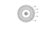
図1は、本発明の実施の形態1に係る光素子モジュール50の断面図である。図2は、図1の光素子モジュール50を使用した光伝送モジュール100の断面図である。図3は、図2の光伝送モジュール100の光素子モジュール50と光ファイバ4との固定部分の断面図である。図4は、図2の光伝送モジュール100の基板1の孔部10を面発光レーザ側2からみた平面図である。
実施の形態2にかかる光伝送モジュールは、ガイド保持部材の貫通孔の両端部にそれぞれテーパが形成されている点で、実施の形態1の光伝送モジュール100と異なる。以下、図面を参照して、実施の形態2にかかる光伝送モジュールを説明する。図5は、実施の形態2に係る光素子モジュール60の断面図である。図6は、実施の形態2で使用するガイド保持部材3Aの斜視図である。図7は、図5の光素子モジュール60に光ファイバ4を挿通固定した光伝送モジュール200の断面図である。なお、図7の光伝送モジュール200は、光素子モジュール60と光ファイバ4で形成されているが、実施の形態1の光伝送モジュール100と同様に、光ファイバ4の他方の端面に、光素子モジュール30を接続した構成としてもよい。
実施の形態3にかかる光伝送モジュールは、基板の孔部周辺に凸上部材が形成されている点で、実施の形態1にかかる光伝送モジュール100と異なる。以下、図面を参照して、実施の形態3にかかる光伝送モジュールを説明する。図10は、実施の形態3に係る光伝送モジュール300の断面図である。図11は、図10の光伝送モジュール300の基板1Aの孔部10を面発光レーザ2側からみた平面図である。なお、図10の光伝送モジュール300は、光素子モジュール70と光ファイバ4で形成されているが、実施の形態1の光伝送モジュール100と同様に、光ファイバ4の他方の端面に、光素子モジュール30を接続した構成としてもよい。
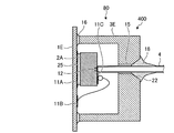
実施の形態4にかかる光伝送モジュール400は、発光部が基板との実装面の反対に位置するように基板に実装されるワイヤボンディングタイプの面発光レーザを光素子として使用する。図15は、実施の形態4に係る光素子モジュール80の断面図である。図16は、図15の光素子モジュール80に光ファイバ4を挿通固定した光伝送モジュール400の断面図である。なお、図16の光伝送モジュール400は、光素子モジュール80と光ファイバ4で形成されているが、実施の形態1の光伝送モジュール100と同様に、光ファイバ4の他方の端面に、光素子モジュール30を接続した構成としてもよい。
2 面発光レーザ
3 ガイド保持部材
4 光ファイバ
10 孔部
11 接続電極
12 発光部
13 Auバンプ
14、16、18 接着剤
15 貫通孔
17 空間
19 コア
20 クラッド
21、22 テーパ
23、24 凸状部材
50 光素子モジュール
100 光伝送モジュール
Claims (11)
- 光信号を入力する受光部または光信号を出力する発光部を有する光素子と、前記光素子が実装される基板と、を備える光素子モジュールにおいて、
前記光素子の受光部または発光部から入出力される光信号を入出力するコアとクラッドからなる光ファイバ挿入用の貫通孔を有し、前記光素子と前記基板の厚さ方向に並べて、接着材を硬化して実装配置されるガイド保持部材を備え、
前記貫通孔は前記光ファイバの外径と略同一径の円柱状であって、前記基板と接する側の端部はテーパ形状をなし、前記貫通孔のテーパ形状内には前記接着剤が留まり、
前記受光部または前記発光部の径は前記光ファイバのコアの径よりも小さいことを特徴とする光素子モジュール。 - 前記光素子は、前記発光部または前記受光部が前記基板と対向するように前記基板にフリップチップ実装され、
前記ガイド保持部材は、前記基板の前記光素子が実装された面とは反対側の面に実装され、
前記基板は、異なる面に位置する前記光素子と前記光ファイバとの間で光信号を送受信する孔部を有することを特徴とする請求項1に記載の光素子モジュール。 - 前記孔部の内径は、前記貫通孔の内径と同径または大きいことを特徴とする請求項2に記載の光素子モジュール。
- 前記貫通孔の光ファイバ挿入口側の端部がテーパ形状をなすことを特徴とする請求項3に記載の光素子モジュール。
- 前記基板の前記光素子の実装面の孔部周辺に、実装面から突起する凸状部材が形成されることを特徴とする請求項2〜4のいずれか一つに記載の光素子モジュール。
- 前記基板の前記ガイド保持部材の実装面の孔部周辺に、実装面から突起する凸状部材が形成されることを特徴とする請求項2〜5のいずれか一つに記載の光素子モジュール。
- 前記貫通孔の前記光素子側端面と前記発光部または前記受光部との間に、挿通する光ファイバの端面から前記発光部または前記受光部までの距離を調整しうる空間を有することを特徴とする請求項2〜5のいずれか一つに記載の光素子モジュール。
- 請求項1〜7のいずれか一つに記載の光素子モジュールを用いた光伝送モジュールであって、さらに、
前記貫通孔に挿入された光ファイバを有し、
前記光ファイバは、前記光ファイバの一方の端面と前記光素子の発光部または受光部とを光学的に位置合わせして前記ガイド保持部材に接合されることを特徴とする光伝送モジュール。 - 前記光ファイバの他方の端面に光学的に位置合わせし、前記光素子の受光部に対し光信号を出力する発光部を有する送信モジュール、または、前記光素子の発光部が出力した光信号を入力する受光部を有する受信モジュールを更に有することを特徴とする請求項8に記載の光伝送モジュール。
- 請求項8または9に記載の光伝送モジュールの製造方法において、
前記基板の表面に前記光素子を実装する光素子実装ステップと、
前記光素子実装ステップの後、前記基板に前記光ファイバの外径と略同一径の円柱状をなす貫通孔を有するガイド保持部材を、前記受光部または前記発光部の中心と前記貫通孔の中心とを位置合わせし、前記ガイド保持部材と前記光素子とが前記基板の厚さ方向に並ぶよう配置して実装するガイド保持部材実装ステップと、
前記光ファイバを前記貫通孔に挿入し、挿通する光ファイバの端面から前記受光部または前記発光部までの距離を調整して前記光ファイバ端面と前記発光部または前記受光部とを光学的に位置合わせした後、前記光ファイバを前記ガイド保持部材に接合する接合ステップと、
を含むことを特徴とする光伝送モジュールの製造方法。 - 前記接合ステップは、前記光ファイバ端面と前記発光部または前記受光部とを接触させて接合することを特徴とする請求項10に記載の光伝送モジュールの製造方法。
Priority Applications (4)
| Application Number | Priority Date | Filing Date | Title |
|---|---|---|---|
| JP2011159847A JP5809866B2 (ja) | 2011-07-21 | 2011-07-21 | 光素子モジュール、光伝送モジュール、および光伝送モジュールの製造方法 |
| PCT/JP2012/068108 WO2013011983A1 (ja) | 2011-07-21 | 2012-07-17 | 光素子モジュール、光伝送モジュール、および光伝送モジュールの製造方法 |
| EP12814657.8A EP2735899B1 (en) | 2011-07-21 | 2012-07-17 | Optical element module, optical transmission module, and method of manufacturing optical transmission module |
| US14/104,345 US9385249B2 (en) | 2011-07-21 | 2013-12-12 | Optical element module, optical transmission module, and method of manufacturing optical transmission module |
Applications Claiming Priority (1)
| Application Number | Priority Date | Filing Date | Title |
|---|---|---|---|
| JP2011159847A JP5809866B2 (ja) | 2011-07-21 | 2011-07-21 | 光素子モジュール、光伝送モジュール、および光伝送モジュールの製造方法 |
Publications (3)
| Publication Number | Publication Date |
|---|---|
| JP2013025092A JP2013025092A (ja) | 2013-02-04 |
| JP2013025092A5 JP2013025092A5 (ja) | 2014-09-04 |
| JP5809866B2 true JP5809866B2 (ja) | 2015-11-11 |
Family
ID=47558160
Family Applications (1)
| Application Number | Title | Priority Date | Filing Date |
|---|---|---|---|
| JP2011159847A Active JP5809866B2 (ja) | 2011-07-21 | 2011-07-21 | 光素子モジュール、光伝送モジュール、および光伝送モジュールの製造方法 |
Country Status (4)
| Country | Link |
|---|---|
| US (1) | US9385249B2 (ja) |
| EP (1) | EP2735899B1 (ja) |
| JP (1) | JP5809866B2 (ja) |
| WO (1) | WO2013011983A1 (ja) |
Families Citing this family (27)
| Publication number | Priority date | Publication date | Assignee | Title |
|---|---|---|---|---|
| JP5996215B2 (ja) * | 2012-02-28 | 2016-09-21 | オリンパス株式会社 | 光電変換モジュールおよび光伝送ユニット |
| JP6321933B2 (ja) * | 2013-09-26 | 2018-05-09 | オリンパス株式会社 | 光伝送モジュール、及び内視鏡 |
| JP6411088B2 (ja) | 2013-09-26 | 2018-10-24 | オリンパス株式会社 | 光伝送モジュールおよび内視鏡 |
| JP6203010B2 (ja) | 2013-11-18 | 2017-09-27 | オリンパス株式会社 | 内視鏡 |
| JP6230388B2 (ja) | 2013-11-28 | 2017-11-15 | オリンパス株式会社 | 内視鏡 |
| JP6226782B2 (ja) | 2014-03-13 | 2017-11-08 | オリンパス株式会社 | 光伝送モジュールおよび光伝送モジュールの製造方法 |
| JP6382586B2 (ja) * | 2014-06-11 | 2018-08-29 | オリンパス株式会社 | 光伝送モジュール、および光伝送モジュールの製造方法 |
| JP6382585B2 (ja) * | 2014-06-11 | 2018-08-29 | オリンパス株式会社 | 光伝送モジュール |
| JP2016004130A (ja) * | 2014-06-16 | 2016-01-12 | オリンパス株式会社 | 光伝送モジュールおよび光伝送モジュールの製造方法 |
| JP6485840B2 (ja) * | 2015-01-23 | 2019-03-20 | オリンパス株式会社 | 光伝送モジュールおよび内視鏡 |
| US9541717B2 (en) | 2015-01-30 | 2017-01-10 | Avago Technologies General IP (Singapore) Pta. Ltd. | Optoelectronic assembly incorporating an optical fiber alignment structure |
| JPWO2016185537A1 (ja) * | 2015-05-18 | 2018-03-01 | オリンパス株式会社 | 内視鏡、および光伝送モジュール |
| JPWO2016189691A1 (ja) * | 2015-05-27 | 2018-03-15 | オリンパス株式会社 | 内視鏡および光伝送モジュール |
| WO2017109930A1 (ja) | 2015-12-25 | 2017-06-29 | オリンパス株式会社 | 撮像モジュールおよび内視鏡 |
| US10186584B2 (en) | 2016-08-18 | 2019-01-22 | Uchicago Argonne, Llc | Systems and methods for forming diamond heterojunction junction devices |
| WO2018134933A1 (ja) * | 2017-01-19 | 2018-07-26 | オリンパス株式会社 | 光モジュールおよび内視鏡 |
| WO2018138778A1 (ja) | 2017-01-24 | 2018-08-02 | オリンパス株式会社 | 内視鏡 |
| US20190129108A1 (en) * | 2017-10-31 | 2019-05-02 | Versalume LLC | Modular Laser Connector Packaging System and Method |
| WO2019163014A1 (ja) * | 2018-02-21 | 2019-08-29 | オリンパス株式会社 | 内視鏡用光モジュール、内視鏡、および内視鏡用光モジュールの製造方法 |
| WO2019207742A1 (ja) * | 2018-04-26 | 2019-10-31 | オリンパス株式会社 | 内視鏡用光モジュール、内視鏡、および内視鏡用光モジュールの製造方法 |
| WO2020075253A1 (ja) | 2018-10-11 | 2020-04-16 | オリンパス株式会社 | 内視鏡用撮像装置、内視鏡、および内視鏡用撮像装置の製造方法 |
| US10551542B1 (en) | 2018-12-11 | 2020-02-04 | Corning Incorporated | Light modules and devices incorporating light modules |
| WO2020217277A1 (ja) * | 2019-04-22 | 2020-10-29 | オリンパス株式会社 | 内視鏡用撮像装置の製造方法、内視鏡用撮像装置、および、内視鏡 |
| CN110412700B (zh) * | 2019-07-26 | 2022-05-17 | 西安微电子技术研究所 | 一种综合电子高速光互连模块集成结构及集成方法 |
| CN114450860A (zh) * | 2019-09-30 | 2022-05-06 | 京瓷株式会社 | 光元件搭载用封装件、电子装置以及电子模块 |
| WO2021260854A1 (ja) * | 2020-06-24 | 2021-12-30 | オリンパス株式会社 | 内視鏡用光モジュール、および、内視鏡 |
| US20220196875A1 (en) * | 2020-12-23 | 2022-06-23 | TE Connectivity Services Gmbh | Light source for an optical sensor |
Family Cites Families (20)
| Publication number | Priority date | Publication date | Assignee | Title |
|---|---|---|---|---|
| JPS594509U (ja) * | 1982-06-29 | 1984-01-12 | 日本板硝子株式会社 | 光ファイバー端子 |
| JPH0538327Y2 (ja) * | 1986-12-26 | 1993-09-28 | ||
| JP3281518B2 (ja) | 1995-09-28 | 2002-05-13 | 京セラ株式会社 | 光通信用モジュール |
| US6243508B1 (en) * | 1999-06-01 | 2001-06-05 | Picolight Incorporated | Electro-opto-mechanical assembly for coupling a light source or receiver to an optical waveguide |
| JP2002250846A (ja) * | 2001-02-26 | 2002-09-06 | Seiko Epson Corp | 光モジュール及びその製造方法並びに光伝達装置 |
| JP2002252430A (ja) * | 2001-02-26 | 2002-09-06 | Ricoh Co Ltd | 光通信システム |
| JP2002311305A (ja) * | 2001-04-13 | 2002-10-23 | Seiko Epson Corp | 光ファイバ支持部材およびこれを用いた光送信装置 |
| US7645076B2 (en) * | 2003-04-29 | 2010-01-12 | Pirelli & C. S.P.A. | Coupling structure for optical fibres and process for making it |
| JP3991318B2 (ja) * | 2004-01-20 | 2007-10-17 | セイコーエプソン株式会社 | 光モジュールの製造方法、光通信装置、電子機器 |
| JP2005286284A (ja) * | 2004-02-03 | 2005-10-13 | Sony Chem Corp | 機能素子実装モジュール並びに光機能素子実装モジュール及びその製造方法 |
| WO2005104314A2 (fr) * | 2004-04-13 | 2005-11-03 | Sa Intexys | Procede de fabrication de circuits electroniques et optoelectroniques |
| US7352935B2 (en) * | 2004-08-17 | 2008-04-01 | Kabushiki Kaisha Toshiba | Optoelectronic conversion header, LSI package with interface module, method of manufacturing optoelectronic conversion header, and optical interconnection system |
| JP4280851B2 (ja) * | 2004-11-18 | 2009-06-17 | 株式会社白山製作所 | 光コネクタおよびその製造方法 |
| WO2007088584A1 (ja) * | 2006-01-31 | 2007-08-09 | Fujitsu Limited | 光モジュールおよびその製造方法 |
| JP4698487B2 (ja) * | 2006-05-29 | 2011-06-08 | 株式会社フジクラ | 光ファイバアレイ |
| JP2009047937A (ja) * | 2007-08-20 | 2009-03-05 | Sony Corp | 光送信/光受信モジュール及び光モジュールの製造方法並びに光通信モジュール |
| JP5049145B2 (ja) * | 2008-01-22 | 2012-10-17 | 日東電工株式会社 | 光導波路デバイスの製法 |
| JP2009206158A (ja) * | 2008-02-26 | 2009-09-10 | Sumitomo Electric Ind Ltd | レーザモジュールおよびレーザ装置 |
| JP2010048940A (ja) * | 2008-08-20 | 2010-03-04 | Fuji Xerox Co Ltd | 光学装置 |
| WO2012006176A1 (en) * | 2010-06-29 | 2012-01-12 | Ultra Communications, Inc. | Low profile fiber-to-module interface with relaxed alignment tolerances |
-
2011
- 2011-07-21 JP JP2011159847A patent/JP5809866B2/ja active Active
-
2012
- 2012-07-17 EP EP12814657.8A patent/EP2735899B1/en not_active Not-in-force
- 2012-07-17 WO PCT/JP2012/068108 patent/WO2013011983A1/ja active Application Filing
-
2013
- 2013-12-12 US US14/104,345 patent/US9385249B2/en active Active
Also Published As
| Publication number | Publication date |
|---|---|
| EP2735899B1 (en) | 2018-09-05 |
| EP2735899A1 (en) | 2014-05-28 |
| US20140097459A1 (en) | 2014-04-10 |
| US9385249B2 (en) | 2016-07-05 |
| JP2013025092A (ja) | 2013-02-04 |
| EP2735899A4 (en) | 2015-03-25 |
| WO2013011983A1 (ja) | 2013-01-24 |
Similar Documents
| Publication | Publication Date | Title |
|---|---|---|
| JP5809866B2 (ja) | 光素子モジュール、光伝送モジュール、および光伝送モジュールの製造方法 | |
| US9762329B2 (en) | Optical transmission module and imaging device | |
| US9207412B2 (en) | Optical transmission module and endoscope | |
| JP6321933B2 (ja) | 光伝送モジュール、及び内視鏡 | |
| JP4793169B2 (ja) | 接続体および光送受信モジュール | |
| US11445898B2 (en) | Optical module for endoscope, endoscope, and manufacturing method for optical module for endoscope | |
| US10088669B2 (en) | Endoscope | |
| WO2009090988A1 (ja) | 光モジュール | |
| JP2009047937A (ja) | 光送信/光受信モジュール及び光モジュールの製造方法並びに光通信モジュール | |
| US20180078114A1 (en) | Endoscope and optical transmission module | |
| WO2018150512A1 (ja) | 光モジュール、内視鏡、および、光モジュールの製造方法 | |
| US20170315310A1 (en) | Optical transmission module and endoscope | |
| WO2019208633A1 (ja) | 内視鏡用光モジュール、内視鏡、および内視鏡用光モジュールの製造方法 | |
| US20180368659A1 (en) | Optical transmitter and endoscope | |
| JP2015097588A (ja) | 光伝送モジュール及び内視鏡 | |
| US20180368662A1 (en) | Optical transmission module and endoscope | |
| JP6081160B2 (ja) | 光素子モジュール、光伝送モジュール、および光伝送モジュールの製造方法 | |
| JP6382585B2 (ja) | 光伝送モジュール | |
| US10838194B2 (en) | Optical transmission module and endoscope | |
| WO2018146806A1 (ja) | 光モジュールおよび内視鏡 | |
| JP2004336025A (ja) | 光モジュール、光モジュール実装基板、光伝送モジュール、双方向光伝送モジュール、光モジュールの製造方法 | |
| JP2018105907A (ja) | 光モジュールおよび内視鏡 |
Legal Events
| Date | Code | Title | Description |
|---|---|---|---|
| A521 | Request for written amendment filed |
Free format text: JAPANESE INTERMEDIATE CODE: A523 Effective date: 20140718 |
|
| A621 | Written request for application examination |
Free format text: JAPANESE INTERMEDIATE CODE: A621 Effective date: 20140718 |
|
| A131 | Notification of reasons for refusal |
Free format text: JAPANESE INTERMEDIATE CODE: A131 Effective date: 20150602 |
|
| A521 | Request for written amendment filed |
Free format text: JAPANESE INTERMEDIATE CODE: A523 Effective date: 20150729 |
|
| TRDD | Decision of grant or rejection written | ||
| A01 | Written decision to grant a patent or to grant a registration (utility model) |
Free format text: JAPANESE INTERMEDIATE CODE: A01 Effective date: 20150818 |
|
| A61 | First payment of annual fees (during grant procedure) |
Free format text: JAPANESE INTERMEDIATE CODE: A61 Effective date: 20150914 |
|
| R151 | Written notification of patent or utility model registration |
Ref document number: 5809866 Country of ref document: JP Free format text: JAPANESE INTERMEDIATE CODE: R151 |
|
| S531 | Written request for registration of change of domicile |
Free format text: JAPANESE INTERMEDIATE CODE: R313531 |
|
| R350 | Written notification of registration of transfer |
Free format text: JAPANESE INTERMEDIATE CODE: R350 |
|
| R250 | Receipt of annual fees |
Free format text: JAPANESE INTERMEDIATE CODE: R250 |
|
| R250 | Receipt of annual fees |
Free format text: JAPANESE INTERMEDIATE CODE: R250 |
|
| R250 | Receipt of annual fees |
Free format text: JAPANESE INTERMEDIATE CODE: R250 |
|
| R250 | Receipt of annual fees |
Free format text: JAPANESE INTERMEDIATE CODE: R250 |
|
| R250 | Receipt of annual fees |
Free format text: JAPANESE INTERMEDIATE CODE: R250 |
|
| R250 | Receipt of annual fees |
Free format text: JAPANESE INTERMEDIATE CODE: R250 |