JP5750466B2 - 静電容量式入力装置 - Google Patents
静電容量式入力装置 Download PDFInfo
- Publication number
- JP5750466B2 JP5750466B2 JP2013041423A JP2013041423A JP5750466B2 JP 5750466 B2 JP5750466 B2 JP 5750466B2 JP 2013041423 A JP2013041423 A JP 2013041423A JP 2013041423 A JP2013041423 A JP 2013041423A JP 5750466 B2 JP5750466 B2 JP 5750466B2
- Authority
- JP
- Japan
- Prior art keywords
- layer
- wiring
- insulating layer
- electrodes
- input device
- Prior art date
- Legal status (The legal status is an assumption and is not a legal conclusion. Google has not performed a legal analysis and makes no representation as to the accuracy of the status listed.)
- Active
Links
Images

Classifications
-
- G—PHYSICS
- G06—COMPUTING OR CALCULATING; COUNTING
- G06F—ELECTRIC DIGITAL DATA PROCESSING
- G06F3/00—Input arrangements for transferring data to be processed into a form capable of being handled by the computer; Output arrangements for transferring data from processing unit to output unit, e.g. interface arrangements
- G06F3/01—Input arrangements or combined input and output arrangements for interaction between user and computer
- G06F3/03—Arrangements for converting the position or the displacement of a member into a coded form
- G06F3/041—Digitisers, e.g. for touch screens or touch pads, characterised by the transducing means
- G06F3/044—Digitisers, e.g. for touch screens or touch pads, characterised by the transducing means by capacitive means
- G06F3/0445—Digitisers, e.g. for touch screens or touch pads, characterised by the transducing means by capacitive means using two or more layers of sensing electrodes, e.g. using two layers of electrodes separated by a dielectric layer
-
- G—PHYSICS
- G06—COMPUTING OR CALCULATING; COUNTING
- G06F—ELECTRIC DIGITAL DATA PROCESSING
- G06F3/00—Input arrangements for transferring data to be processed into a form capable of being handled by the computer; Output arrangements for transferring data from processing unit to output unit, e.g. interface arrangements
- G06F3/01—Input arrangements or combined input and output arrangements for interaction between user and computer
- G06F3/03—Arrangements for converting the position or the displacement of a member into a coded form
- G06F3/041—Digitisers, e.g. for touch screens or touch pads, characterised by the transducing means
- G06F3/044—Digitisers, e.g. for touch screens or touch pads, characterised by the transducing means by capacitive means
- G06F3/0446—Digitisers, e.g. for touch screens or touch pads, characterised by the transducing means by capacitive means using a grid-like structure of electrodes in at least two directions, e.g. using row and column electrodes
-
- H—ELECTRICITY
- H01—ELECTRIC ELEMENTS
- H01B—CABLES; CONDUCTORS; INSULATORS; SELECTION OF MATERIALS FOR THEIR CONDUCTIVE, INSULATING OR DIELECTRIC PROPERTIES
- H01B5/00—Non-insulated conductors or conductive bodies characterised by their form
- H01B5/14—Non-insulated conductors or conductive bodies characterised by their form comprising conductive layers or films on insulating-supports
-
- G—PHYSICS
- G06—COMPUTING OR CALCULATING; COUNTING
- G06F—ELECTRIC DIGITAL DATA PROCESSING
- G06F2203/00—Indexing scheme relating to G06F3/00 - G06F3/048
- G06F2203/041—Indexing scheme relating to G06F3/041 - G06F3/045
- G06F2203/04111—Cross over in capacitive digitiser, i.e. details of structures for connecting electrodes of the sensing pattern where the connections cross each other, e.g. bridge structures comprising an insulating layer, or vias through substrate
Landscapes
- Engineering & Computer Science (AREA)
- General Engineering & Computer Science (AREA)
- Theoretical Computer Science (AREA)
- Human Computer Interaction (AREA)
- Physics & Mathematics (AREA)
- General Physics & Mathematics (AREA)
- Position Input By Displaying (AREA)
- Switches That Are Operated By Magnetic Or Electric Fields (AREA)
Description
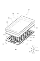
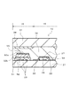
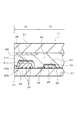
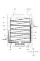
図1は、第1の実施形態の静電容量式入力装置を示す分解斜視図である。図1に示すように本実施形態の静電容量式入力装置10は、入力位置情報を検出する静電容量式センサ部20と、表面パネル31とを有して構成される。表面パネル31は、静電容量式センサ部20に対して入力操作側(図1のZ1方向)に配置されており、静電容量式センサ部20と表面パネル31とは粘着層32を介して貼り合わされる。
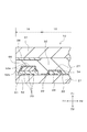
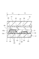
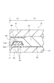
図8は、第2の実施形態の静電容量式入力装置を示す、部分拡大断面図である。第2の実施形態の静電容量式入力装置11は、図8に示すように、配線29の上に設けられた配線部絶縁層51と嵩上げ層52の構成が異なっており、入力領域15における第1の電極22、第2の電極24(図8には接続部28のみ示す)等のパターンは、図2に示す第1の実施形態と同様である。
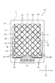
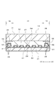
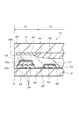
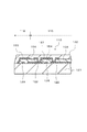
図9は、第3の実施形態の静電容量式入力装置における、基材、及び基材に形成された各電極、配線を示す平面図である。図10は、図9に示す基材を表面パネルに貼り合わせて静電容量式入力装置としたときに、図9のX−X線の位置で切断して矢印方向から見たときの部分拡大断面図である。
15 入力領域
16 非入力領域
20 静電容量式センサ部
21 基材
22、23 第1の電極
24、25 第2の電極
26 電極
27 ブリッジ部
28 接続部
29 配線
31 表面パネル
32 粘着層
35 第1の透明充填層
36 第2の透明充填層
38 加飾層
51 配線部絶縁層
52 嵩上げ層
54 交差部絶縁層
55 導体層
Claims (5)
- 基材と、複数の電極と、前記電極に接続された配線と、導体層と、を有し、
前記基材において、入力操作を行う入力領域と、前記入力領域の外側の非入力領域とが設定されており、
複数の前記電極は前記基材の前記入力領域に形成されるとともに、前記配線は前記基材の非入力領域に形成されており、
前記導体層は、前記配線に対して重なる位置に配置されて、
前記導体層と前記配線との間に配線部絶縁層と嵩上げ層とが積層されており、
前記嵩上げ層の厚さは、前記配線部絶縁層の厚さよりも厚いことを特徴とすることを特徴とする静電容量式入力装置。 - 前記配線の上に前記配線部絶縁層が形成されて、前記配線部絶縁層の上に前記嵩上げ層が形成されており、
前記導体層は前記嵩上げ層を覆うように形成されていることを特徴とする請求項1に記載の静電容量式入力装置。 - 前記配線の上に前記嵩上げ層が形成されて、前記嵩上げ層の上に前記配線部絶縁層が形成されており、
前記配線部絶縁層は前記嵩上げ層を覆うように形成されていることを特徴とする請求項1に記載の静電容量式入力装置。 - 前記複数の電極は、透光性の複数の第1の電極及び複数の第2の電極を有して構成され、
前記第1の電極は、前記基材面内の第1の方向において間隔を設けて配置されるとともに、隣り合う前記第1の電極同士はブリッジ部によって接続されており、
前記第2の電極は、前記第1の方向に交差する第2の方向において間隔を設けて配置されるとともに、隣り合う前記第2の電極同士は接続部によって接続されており、
前記接続部を覆うように交差部絶縁層が形成されて、前記ブリッジ部は、前記接続部に対して平面視で交差するように前記接続部及び前記交差部絶縁層を跨がって形成されており、
前記導体層と前記配線との距離は、前記ブリッジ部と前記接続部との距離よりも大きいことを特徴とする請求項1から請求項3のいずれか1項に記載の静電容量式入力装置。 - 前記交差部絶縁層と前記配線部絶縁層とは同じ材料により形成されていることを特徴とする請求項4に記載の静電容量式入力装置。
Priority Applications (3)
| Application Number | Priority Date | Filing Date | Title |
|---|---|---|---|
| JP2013041423A JP5750466B2 (ja) | 2013-03-04 | 2013-03-04 | 静電容量式入力装置 |
| CN201420042408.0U CN203746045U (zh) | 2013-03-04 | 2014-01-23 | 静电电容式输入装置 |
| KR1020140012256A KR101609040B1 (ko) | 2013-03-04 | 2014-02-03 | 정전 용량식 입력 장치 |
Applications Claiming Priority (1)
| Application Number | Priority Date | Filing Date | Title |
|---|---|---|---|
| JP2013041423A JP5750466B2 (ja) | 2013-03-04 | 2013-03-04 | 静電容量式入力装置 |
Related Child Applications (1)
| Application Number | Title | Priority Date | Filing Date |
|---|---|---|---|
| JP2015082473A Division JP5908637B2 (ja) | 2015-04-14 | 2015-04-14 | 静電容量式入力装置 |
Publications (2)
| Publication Number | Publication Date |
|---|---|
| JP2014170342A JP2014170342A (ja) | 2014-09-18 |
| JP5750466B2 true JP5750466B2 (ja) | 2015-07-22 |
Family
ID=51345819
Family Applications (1)
| Application Number | Title | Priority Date | Filing Date |
|---|---|---|---|
| JP2013041423A Active JP5750466B2 (ja) | 2013-03-04 | 2013-03-04 | 静電容量式入力装置 |
Country Status (3)
| Country | Link |
|---|---|
| JP (1) | JP5750466B2 (ja) |
| KR (1) | KR101609040B1 (ja) |
| CN (1) | CN203746045U (ja) |
Families Citing this family (6)
| Publication number | Priority date | Publication date | Assignee | Title |
|---|---|---|---|---|
| KR102288825B1 (ko) * | 2015-01-13 | 2021-08-11 | 엘지이노텍 주식회사 | 터치 윈도우 |
| KR102002882B1 (ko) * | 2015-06-14 | 2019-07-24 | 주식회사 엘지화학 | 터치 센서 및 이의 제조방법 |
| CN106249975B (zh) * | 2016-08-12 | 2018-11-06 | 京东方科技集团股份有限公司 | 一种触控屏、显示装置及触控屏的制作方法 |
| BR112020014345B1 (pt) | 2018-01-24 | 2023-09-26 | Matsutani Chemical Industry Co., Ltd | Cetose 3-epimerase variante e método para produzir d- psicose |
| KR101977548B1 (ko) | 2018-12-11 | 2019-05-10 | 화신주방산업(주) | 조임 온도센서를 갖는 주물 조리용 솥 |
| KR102856926B1 (ko) * | 2019-10-30 | 2025-09-08 | 삼성디스플레이 주식회사 | 디지타이저를 포함하는 플렉서블 표시 장치 및 터치 위치 감지 방법 |
Family Cites Families (3)
| Publication number | Priority date | Publication date | Assignee | Title |
|---|---|---|---|---|
| TW564564B (en) | 2002-10-03 | 2003-12-01 | Au Optronics Corp | Pixel structure and fabricating method thereof |
| JP5300640B2 (ja) | 2009-07-27 | 2013-09-25 | 株式会社ジャパンディスプレイウェスト | 静電容量型入力装置および入力装置付き電気光学装置 |
| JP2013012182A (ja) * | 2011-05-27 | 2013-01-17 | Kyocera Corp | 入力装置、表示装置、および電子機器 |
-
2013
- 2013-03-04 JP JP2013041423A patent/JP5750466B2/ja active Active
-
2014
- 2014-01-23 CN CN201420042408.0U patent/CN203746045U/zh not_active Expired - Lifetime
- 2014-02-03 KR KR1020140012256A patent/KR101609040B1/ko active Active
Also Published As
| Publication number | Publication date |
|---|---|
| CN203746045U (zh) | 2014-07-30 |
| JP2014170342A (ja) | 2014-09-18 |
| KR20140109254A (ko) | 2014-09-15 |
| KR101609040B1 (ko) | 2016-04-04 |
Similar Documents
| Publication | Publication Date | Title |
|---|---|---|
| KR101598412B1 (ko) | 전극 시트 및 터치 입력 장치 | |
| TWI585659B (zh) | 電容式觸控面板及降低電容式觸控面板的金屬導體可見度之觸控面板的製造方法 | |
| JP4965006B2 (ja) | 透光型入力装置およびその製造方法 | |
| CN102253752B (zh) | 触摸面板以及触摸显示面板 | |
| US20150075959A1 (en) | Touch panel | |
| JP5750466B2 (ja) | 静電容量式入力装置 | |
| JP2010182277A (ja) | 入力装置 | |
| TW201530404A (zh) | 觸控面板 | |
| JP6418910B2 (ja) | タッチスクリーン、タッチパネル及び表示装置 | |
| CN101419521A (zh) | 触控式基板与触控式液晶显示器 | |
| JP2017207816A (ja) | タッチパネル | |
| JP5520162B2 (ja) | 入力装置及びその製造方法 | |
| JP2012022427A (ja) | 静電容量式入力装置 | |
| JP5472858B2 (ja) | タッチスイッチ | |
| JP5846953B2 (ja) | 入力装置及びその製造方法 | |
| JP2014170334A (ja) | 静電容量式タッチパネルおよびそれを用いた手持ち式電子機器 | |
| JP2015011493A (ja) | 入力装置 | |
| CN205507728U (zh) | 触控面板 | |
| JP7026525B2 (ja) | センサ装置 | |
| JPWO2017183315A1 (ja) | 静電容量式センサ | |
| JP2017021631A (ja) | 静電容量式入力装置 | |
| TWI606377B (zh) | 觸控面板 | |
| JP5908637B2 (ja) | 静電容量式入力装置 | |
| JP2015011492A (ja) | 入力装置及びその製造方法 | |
| JP2017068819A (ja) | タッチパネル |
Legal Events
| Date | Code | Title | Description |
|---|---|---|---|
| RD02 | Notification of acceptance of power of attorney |
Free format text: JAPANESE INTERMEDIATE CODE: A7422 Effective date: 20140904 |
|
| A621 | Written request for application examination |
Free format text: JAPANESE INTERMEDIATE CODE: A621 Effective date: 20141023 |
|
| A131 | Notification of reasons for refusal |
Free format text: JAPANESE INTERMEDIATE CODE: A131 Effective date: 20150324 |
|
| A977 | Report on retrieval |
Free format text: JAPANESE INTERMEDIATE CODE: A971007 Effective date: 20150325 |
|
| A521 | Written amendment |
Free format text: JAPANESE INTERMEDIATE CODE: A523 Effective date: 20150414 |
|
| TRDD | Decision of grant or rejection written | ||
| A01 | Written decision to grant a patent or to grant a registration (utility model) |
Free format text: JAPANESE INTERMEDIATE CODE: A01 Effective date: 20150512 |
|
| A61 | First payment of annual fees (during grant procedure) |
Free format text: JAPANESE INTERMEDIATE CODE: A61 Effective date: 20150518 |
|
| R150 | Certificate of patent or registration of utility model |
Ref document number: 5750466 Country of ref document: JP Free format text: JAPANESE INTERMEDIATE CODE: R150 |
|
| S533 | Written request for registration of change of name |
Free format text: JAPANESE INTERMEDIATE CODE: R313533 |
|
| R350 | Written notification of registration of transfer |
Free format text: JAPANESE INTERMEDIATE CODE: R350 |