JP5747027B2 - 図形を有する電子ディスプレイ及び金属微小パターン化基材 - Google Patents
図形を有する電子ディスプレイ及び金属微小パターン化基材 Download PDFInfo
- Publication number
- JP5747027B2 JP5747027B2 JP2012517591A JP2012517591A JP5747027B2 JP 5747027 B2 JP5747027 B2 JP 5747027B2 JP 2012517591 A JP2012517591 A JP 2012517591A JP 2012517591 A JP2012517591 A JP 2012517591A JP 5747027 B2 JP5747027 B2 JP 5747027B2
- Authority
- JP
- Japan
- Prior art keywords
- micropattern
- metal
- graphic
- features
- continuous
- Prior art date
- Legal status (The legal status is an assumption and is not a legal conclusion. Google has not performed a legal analysis and makes no representation as to the accuracy of the status listed.)
- Expired - Fee Related
Links
- 229910052751 metal Inorganic materials 0.000 title claims description 227
- 239000002184 metal Substances 0.000 title claims description 227
- 239000000758 substrate Substances 0.000 title claims description 76
- 239000013545 self-assembled monolayer Substances 0.000 description 27
- 239000002094 self assembled monolayer Substances 0.000 description 24
- 239000010408 film Substances 0.000 description 18
- 238000000034 method Methods 0.000 description 15
- 238000013461 design Methods 0.000 description 13
- 239000004205 dimethyl polysiloxane Substances 0.000 description 13
- 238000005530 etching Methods 0.000 description 13
- 229920000435 poly(dimethylsiloxane) Polymers 0.000 description 13
- 239000011248 coating agent Substances 0.000 description 12
- 238000000576 coating method Methods 0.000 description 12
- 229920006254 polymer film Polymers 0.000 description 11
- -1 polydimethylsiloxane Polymers 0.000 description 10
- 239000000463 material Substances 0.000 description 9
- 238000000879 optical micrograph Methods 0.000 description 9
- UMGDCJDMYOKAJW-UHFFFAOYSA-N thiourea Chemical compound NC(N)=S UMGDCJDMYOKAJW-UHFFFAOYSA-N 0.000 description 9
- 239000000203 mixture Substances 0.000 description 8
- 125000004429 atom Chemical group 0.000 description 7
- BQCADISMDOOEFD-UHFFFAOYSA-N Silver Chemical compound [Ag] BQCADISMDOOEFD-UHFFFAOYSA-N 0.000 description 6
- 230000000694 effects Effects 0.000 description 6
- 229910052709 silver Inorganic materials 0.000 description 6
- 239000004332 silver Substances 0.000 description 6
- 239000002904 solvent Substances 0.000 description 6
- RYGMFSIKBFXOCR-UHFFFAOYSA-N Copper Chemical compound [Cu] RYGMFSIKBFXOCR-UHFFFAOYSA-N 0.000 description 5
- 229910052802 copper Inorganic materials 0.000 description 5
- 239000010949 copper Substances 0.000 description 5
- 239000010410 layer Substances 0.000 description 5
- 150000002739 metals Chemical class 0.000 description 5
- 238000000813 microcontact printing Methods 0.000 description 5
- 229920002120 photoresistant polymer Polymers 0.000 description 5
- 238000007639 printing Methods 0.000 description 5
- 238000002834 transmittance Methods 0.000 description 5
- PXHVJJICTQNCMI-UHFFFAOYSA-N Nickel Chemical compound [Ni] PXHVJJICTQNCMI-UHFFFAOYSA-N 0.000 description 4
- KDLHZDBZIXYQEI-UHFFFAOYSA-N Palladium Chemical compound [Pd] KDLHZDBZIXYQEI-UHFFFAOYSA-N 0.000 description 4
- WYURNTSHIVDZCO-UHFFFAOYSA-N Tetrahydrofuran Chemical compound C1CCOC1 WYURNTSHIVDZCO-UHFFFAOYSA-N 0.000 description 4
- XSQUKJJJFZCRTK-UHFFFAOYSA-N Urea Natural products NC(N)=O XSQUKJJJFZCRTK-UHFFFAOYSA-N 0.000 description 4
- 150000001875 compounds Chemical class 0.000 description 4
- 229920001971 elastomer Polymers 0.000 description 4
- 239000000806 elastomer Substances 0.000 description 4
- 239000007800 oxidant agent Substances 0.000 description 4
- 238000000206 photolithography Methods 0.000 description 4
- 239000002356 single layer Substances 0.000 description 4
- WEVYAHXRMPXWCK-UHFFFAOYSA-N Acetonitrile Chemical compound CC#N WEVYAHXRMPXWCK-UHFFFAOYSA-N 0.000 description 3
- XEKOWRVHYACXOJ-UHFFFAOYSA-N Ethyl acetate Chemical compound CCOC(C)=O XEKOWRVHYACXOJ-UHFFFAOYSA-N 0.000 description 3
- ZMXDDKWLCZADIW-UHFFFAOYSA-N N,N-Dimethylformamide Chemical compound CN(C)C=O ZMXDDKWLCZADIW-UHFFFAOYSA-N 0.000 description 3
- 150000001356 alkyl thiols Chemical class 0.000 description 3
- 230000005540 biological transmission Effects 0.000 description 3
- PCHJSUWPFVWCPO-UHFFFAOYSA-N gold Chemical compound [Au] PCHJSUWPFVWCPO-UHFFFAOYSA-N 0.000 description 3
- 229910052737 gold Inorganic materials 0.000 description 3
- 239000010931 gold Substances 0.000 description 3
- 238000005286 illumination Methods 0.000 description 3
- 230000003287 optical effect Effects 0.000 description 3
- 230000002093 peripheral effect Effects 0.000 description 3
- 229920000139 polyethylene terephthalate Polymers 0.000 description 3
- 239000005020 polyethylene terephthalate Substances 0.000 description 3
- 230000008569 process Effects 0.000 description 3
- 241000894007 species Species 0.000 description 3
- 239000000126 substance Substances 0.000 description 3
- 229910052717 sulfur Inorganic materials 0.000 description 3
- 238000001039 wet etching Methods 0.000 description 3
- IJGRMHOSHXDMSA-UHFFFAOYSA-N Atomic nitrogen Chemical compound N#N IJGRMHOSHXDMSA-UHFFFAOYSA-N 0.000 description 2
- IAZDPXIOMUYVGZ-UHFFFAOYSA-N Dimethylsulphoxide Chemical compound CS(C)=O IAZDPXIOMUYVGZ-UHFFFAOYSA-N 0.000 description 2
- LFQSCWFLJHTTHZ-UHFFFAOYSA-N Ethanol Chemical compound CCO LFQSCWFLJHTTHZ-UHFFFAOYSA-N 0.000 description 2
- VTLYFUHAOXGGBS-UHFFFAOYSA-N Fe3+ Chemical compound [Fe+3] VTLYFUHAOXGGBS-UHFFFAOYSA-N 0.000 description 2
- XEEYBQQBJWHFJM-UHFFFAOYSA-N Iron Chemical compound [Fe] XEEYBQQBJWHFJM-UHFFFAOYSA-N 0.000 description 2
- BZLVMXJERCGZMT-UHFFFAOYSA-N Methyl tert-butyl ether Chemical compound COC(C)(C)C BZLVMXJERCGZMT-UHFFFAOYSA-N 0.000 description 2
- XUIMIQQOPSSXEZ-UHFFFAOYSA-N Silicon Chemical compound [Si] XUIMIQQOPSSXEZ-UHFFFAOYSA-N 0.000 description 2
- ATJFFYVFTNAWJD-UHFFFAOYSA-N Tin Chemical compound [Sn] ATJFFYVFTNAWJD-UHFFFAOYSA-N 0.000 description 2
- 125000000217 alkyl group Chemical group 0.000 description 2
- 239000000956 alloy Substances 0.000 description 2
- 229910045601 alloy Inorganic materials 0.000 description 2
- 229910052782 aluminium Inorganic materials 0.000 description 2
- XAGFODPZIPBFFR-UHFFFAOYSA-N aluminium Chemical compound [Al] XAGFODPZIPBFFR-UHFFFAOYSA-N 0.000 description 2
- IISBACLAFKSPIT-UHFFFAOYSA-N bisphenol A Chemical compound C=1C=C(O)C=CC=1C(C)(C)C1=CC=C(O)C=C1 IISBACLAFKSPIT-UHFFFAOYSA-N 0.000 description 2
- 125000004432 carbon atom Chemical group C* 0.000 description 2
- 238000006243 chemical reaction Methods 0.000 description 2
- 230000007423 decrease Effects 0.000 description 2
- 125000001495 ethyl group Chemical group [H]C([H])([H])C([H])([H])* 0.000 description 2
- 229910001447 ferric ion Inorganic materials 0.000 description 2
- SZQUEWJRBJDHSM-UHFFFAOYSA-N iron(3+);trinitrate;nonahydrate Chemical compound O.O.O.O.O.O.O.O.O.[Fe+3].[O-][N+]([O-])=O.[O-][N+]([O-])=O.[O-][N+]([O-])=O SZQUEWJRBJDHSM-UHFFFAOYSA-N 0.000 description 2
- 239000004973 liquid crystal related substance Substances 0.000 description 2
- 239000011104 metalized film Substances 0.000 description 2
- 238000001465 metallisation Methods 0.000 description 2
- 125000002496 methyl group Chemical group [H]C([H])([H])* 0.000 description 2
- 238000000465 moulding Methods 0.000 description 2
- 229910052759 nickel Inorganic materials 0.000 description 2
- 229910052763 palladium Inorganic materials 0.000 description 2
- BASFCYQUMIYNBI-UHFFFAOYSA-N platinum Chemical compound [Pt] BASFCYQUMIYNBI-UHFFFAOYSA-N 0.000 description 2
- 230000010287 polarization Effects 0.000 description 2
- 239000004417 polycarbonate Substances 0.000 description 2
- 229920000515 polycarbonate Polymers 0.000 description 2
- 229920000642 polymer Polymers 0.000 description 2
- 229920001296 polysiloxane Polymers 0.000 description 2
- 238000005096 rolling process Methods 0.000 description 2
- 229910052710 silicon Inorganic materials 0.000 description 2
- 239000010703 silicon Substances 0.000 description 2
- 125000004434 sulfur atom Chemical group 0.000 description 2
- YLQBMQCUIZJEEH-UHFFFAOYSA-N tetrahydrofuran Natural products C=1C=COC=1 YLQBMQCUIZJEEH-UHFFFAOYSA-N 0.000 description 2
- 229920001169 thermoplastic Polymers 0.000 description 2
- 239000004416 thermosoftening plastic Substances 0.000 description 2
- 150000007944 thiolates Chemical class 0.000 description 2
- 229910052718 tin Inorganic materials 0.000 description 2
- 239000011135 tin Substances 0.000 description 2
- XLYOFNOQVPJJNP-UHFFFAOYSA-N water Substances O XLYOFNOQVPJJNP-UHFFFAOYSA-N 0.000 description 2
- 239000004986 Cholesteric liquid crystals (ChLC) Substances 0.000 description 1
- XFXPMWWXUTWYJX-UHFFFAOYSA-N Cyanide Chemical compound N#[C-] XFXPMWWXUTWYJX-UHFFFAOYSA-N 0.000 description 1
- 229920002943 EPDM rubber Polymers 0.000 description 1
- 206010073306 Exposure to radiation Diseases 0.000 description 1
- 238000004566 IR spectroscopy Methods 0.000 description 1
- FXHOOIRPVKKKFG-UHFFFAOYSA-N N,N-Dimethylacetamide Chemical compound CN(C)C(C)=O FXHOOIRPVKKKFG-UHFFFAOYSA-N 0.000 description 1
- 239000004952 Polyamide Substances 0.000 description 1
- 239000004698 Polyethylene Substances 0.000 description 1
- 239000004642 Polyimide Substances 0.000 description 1
- 239000004743 Polypropylene Substances 0.000 description 1
- 239000004372 Polyvinyl alcohol Substances 0.000 description 1
- NINIDFKCEFEMDL-UHFFFAOYSA-N Sulfur Chemical compound [S] NINIDFKCEFEMDL-UHFFFAOYSA-N 0.000 description 1
- 238000004833 X-ray photoelectron spectroscopy Methods 0.000 description 1
- 230000009471 action Effects 0.000 description 1
- 230000001154 acute effect Effects 0.000 description 1
- 239000000654 additive Substances 0.000 description 1
- 239000000853 adhesive Substances 0.000 description 1
- 230000001070 adhesive effect Effects 0.000 description 1
- 239000012790 adhesive layer Substances 0.000 description 1
- 150000001298 alcohols Chemical class 0.000 description 1
- 230000003373 anti-fouling effect Effects 0.000 description 1
- 239000003125 aqueous solvent Substances 0.000 description 1
- 150000001491 aromatic compounds Chemical class 0.000 description 1
- QVGXLLKOCUKJST-UHFFFAOYSA-N atomic oxygen Chemical compound [O] QVGXLLKOCUKJST-UHFFFAOYSA-N 0.000 description 1
- 229910052799 carbon Inorganic materials 0.000 description 1
- 125000003178 carboxy group Chemical group [H]OC(*)=O 0.000 description 1
- 230000008859 change Effects 0.000 description 1
- 238000003486 chemical etching Methods 0.000 description 1
- 238000000224 chemical solution deposition Methods 0.000 description 1
- 238000005229 chemical vapour deposition Methods 0.000 description 1
- 239000003086 colorant Substances 0.000 description 1
- 230000000536 complexating effect Effects 0.000 description 1
- 239000002131 composite material Substances 0.000 description 1
- 239000013039 cover film Substances 0.000 description 1
- 239000008367 deionised water Substances 0.000 description 1
- 229910021641 deionized water Inorganic materials 0.000 description 1
- 239000002274 desiccant Substances 0.000 description 1
- 238000000979 dip-pen nanolithography Methods 0.000 description 1
- 239000006185 dispersion Substances 0.000 description 1
- 238000004090 dissolution Methods 0.000 description 1
- 150000002019 disulfides Chemical class 0.000 description 1
- 238000007772 electroless plating Methods 0.000 description 1
- 230000008020 evaporation Effects 0.000 description 1
- 238000001704 evaporation Methods 0.000 description 1
- YAGKRVSRTSUGEY-UHFFFAOYSA-N ferricyanide Chemical compound [Fe+3].N#[C-].N#[C-].N#[C-].N#[C-].N#[C-].N#[C-] YAGKRVSRTSUGEY-UHFFFAOYSA-N 0.000 description 1
- 239000000835 fiber Substances 0.000 description 1
- 238000009472 formulation Methods 0.000 description 1
- 239000011521 glass Substances 0.000 description 1
- 230000004409 healthy vision Effects 0.000 description 1
- 150000002391 heterocyclic compounds Chemical class 0.000 description 1
- 125000004435 hydrogen atom Chemical group [H]* 0.000 description 1
- 229910052738 indium Inorganic materials 0.000 description 1
- APFVFJFRJDLVQX-UHFFFAOYSA-N indium atom Chemical compound [In] APFVFJFRJDLVQX-UHFFFAOYSA-N 0.000 description 1
- 238000007641 inkjet printing Methods 0.000 description 1
- 229910000765 intermetallic Inorganic materials 0.000 description 1
- 229910052742 iron Inorganic materials 0.000 description 1
- 230000001788 irregular Effects 0.000 description 1
- 150000002576 ketones Chemical class 0.000 description 1
- 239000007788 liquid Substances 0.000 description 1
- 238000004519 manufacturing process Methods 0.000 description 1
- 238000004949 mass spectrometry Methods 0.000 description 1
- 238000005259 measurement Methods 0.000 description 1
- 229910001092 metal group alloy Inorganic materials 0.000 description 1
- 229910052976 metal sulfide Inorganic materials 0.000 description 1
- 125000000325 methylidene group Chemical group [H]C([H])=* 0.000 description 1
- 238000001000 micrograph Methods 0.000 description 1
- 230000004048 modification Effects 0.000 description 1
- 238000012986 modification Methods 0.000 description 1
- 229910052754 neon Inorganic materials 0.000 description 1
- GKAOGPIIYCISHV-UHFFFAOYSA-N neon atom Chemical compound [Ne] GKAOGPIIYCISHV-UHFFFAOYSA-N 0.000 description 1
- 150000004767 nitrides Chemical class 0.000 description 1
- 229910052757 nitrogen Inorganic materials 0.000 description 1
- 150000002898 organic sulfur compounds Chemical class 0.000 description 1
- 230000001590 oxidative effect Effects 0.000 description 1
- 229910052760 oxygen Inorganic materials 0.000 description 1
- 239000001301 oxygen Substances 0.000 description 1
- 229910052697 platinum Inorganic materials 0.000 description 1
- 229920003229 poly(methyl methacrylate) Polymers 0.000 description 1
- 229920000058 polyacrylate Polymers 0.000 description 1
- 229920002647 polyamide Polymers 0.000 description 1
- 229920000728 polyester Polymers 0.000 description 1
- 229920000573 polyethylene Polymers 0.000 description 1
- 229920001721 polyimide Polymers 0.000 description 1
- 239000004926 polymethyl methacrylate Substances 0.000 description 1
- 229920000098 polyolefin Polymers 0.000 description 1
- 229920001155 polypropylene Polymers 0.000 description 1
- 229920002635 polyurethane Polymers 0.000 description 1
- 239000004814 polyurethane Substances 0.000 description 1
- 229920002451 polyvinyl alcohol Polymers 0.000 description 1
- 239000004800 polyvinyl chloride Substances 0.000 description 1
- 229920000915 polyvinyl chloride Polymers 0.000 description 1
- 229920002981 polyvinylidene fluoride Polymers 0.000 description 1
- 230000001681 protective effect Effects 0.000 description 1
- 238000004451 qualitative analysis Methods 0.000 description 1
- 230000009467 reduction Effects 0.000 description 1
- 230000002787 reinforcement Effects 0.000 description 1
- 230000000717 retained effect Effects 0.000 description 1
- 229910052703 rhodium Inorganic materials 0.000 description 1
- 239000010948 rhodium Substances 0.000 description 1
- MHOVAHRLVXNVSD-UHFFFAOYSA-N rhodium atom Chemical compound [Rh] MHOVAHRLVXNVSD-UHFFFAOYSA-N 0.000 description 1
- 238000000682 scanning probe acoustic microscopy Methods 0.000 description 1
- 238000001004 secondary ion mass spectrometry Methods 0.000 description 1
- 150000003384 small molecules Chemical class 0.000 description 1
- 230000003595 spectral effect Effects 0.000 description 1
- 238000004544 sputter deposition Methods 0.000 description 1
- 239000003381 stabilizer Substances 0.000 description 1
- 238000003756 stirring Methods 0.000 description 1
- 125000001424 substituent group Chemical group 0.000 description 1
- 238000006467 substitution reaction Methods 0.000 description 1
- 150000004763 sulfides Chemical class 0.000 description 1
- 239000011593 sulfur Substances 0.000 description 1
- 238000004416 surface enhanced Raman spectroscopy Methods 0.000 description 1
- 229910052715 tantalum Inorganic materials 0.000 description 1
- GUVRBAGPIYLISA-UHFFFAOYSA-N tantalum atom Chemical compound [Ta] GUVRBAGPIYLISA-UHFFFAOYSA-N 0.000 description 1
- 238000002207 thermal evaporation Methods 0.000 description 1
- 229920005992 thermoplastic resin Polymers 0.000 description 1
- 229920001187 thermosetting polymer Polymers 0.000 description 1
- 239000004634 thermosetting polymer Substances 0.000 description 1
- 150000003556 thioamides Chemical class 0.000 description 1
- 150000003573 thiols Chemical class 0.000 description 1
- 150000003585 thioureas Chemical class 0.000 description 1
- 238000012546 transfer Methods 0.000 description 1
- 238000009827 uniform distribution Methods 0.000 description 1
- 230000000007 visual effect Effects 0.000 description 1
- 239000012991 xanthate Substances 0.000 description 1
Images


Classifications
-
- H—ELECTRICITY
- H05—ELECTRIC TECHNIQUES NOT OTHERWISE PROVIDED FOR
- H05K—PRINTED CIRCUITS; CASINGS OR CONSTRUCTIONAL DETAILS OF ELECTRIC APPARATUS; MANUFACTURE OF ASSEMBLAGES OF ELECTRICAL COMPONENTS
- H05K1/00—Printed circuits
- H05K1/02—Details
- H05K1/0296—Conductive pattern lay-out details not covered by sub groups H05K1/02 - H05K1/0295
-
- C—CHEMISTRY; METALLURGY
- C23—COATING METALLIC MATERIAL; COATING MATERIAL WITH METALLIC MATERIAL; CHEMICAL SURFACE TREATMENT; DIFFUSION TREATMENT OF METALLIC MATERIAL; COATING BY VACUUM EVAPORATION, BY SPUTTERING, BY ION IMPLANTATION OR BY CHEMICAL VAPOUR DEPOSITION, IN GENERAL; INHIBITING CORROSION OF METALLIC MATERIAL OR INCRUSTATION IN GENERAL
- C23F—NON-MECHANICAL REMOVAL OF METALLIC MATERIAL FROM SURFACE; INHIBITING CORROSION OF METALLIC MATERIAL OR INCRUSTATION IN GENERAL; MULTI-STEP PROCESSES FOR SURFACE TREATMENT OF METALLIC MATERIAL INVOLVING AT LEAST ONE PROCESS PROVIDED FOR IN CLASS C23 AND AT LEAST ONE PROCESS COVERED BY SUBCLASS C21D OR C22F OR CLASS C25
- C23F1/00—Etching metallic material by chemical means
- C23F1/02—Local etching
-
- C—CHEMISTRY; METALLURGY
- C23—COATING METALLIC MATERIAL; COATING MATERIAL WITH METALLIC MATERIAL; CHEMICAL SURFACE TREATMENT; DIFFUSION TREATMENT OF METALLIC MATERIAL; COATING BY VACUUM EVAPORATION, BY SPUTTERING, BY ION IMPLANTATION OR BY CHEMICAL VAPOUR DEPOSITION, IN GENERAL; INHIBITING CORROSION OF METALLIC MATERIAL OR INCRUSTATION IN GENERAL
- C23F—NON-MECHANICAL REMOVAL OF METALLIC MATERIAL FROM SURFACE; INHIBITING CORROSION OF METALLIC MATERIAL OR INCRUSTATION IN GENERAL; MULTI-STEP PROCESSES FOR SURFACE TREATMENT OF METALLIC MATERIAL INVOLVING AT LEAST ONE PROCESS PROVIDED FOR IN CLASS C23 AND AT LEAST ONE PROCESS COVERED BY SUBCLASS C21D OR C22F OR CLASS C25
- C23F1/00—Etching metallic material by chemical means
- C23F1/10—Etching compositions
- C23F1/14—Aqueous compositions
-
- G—PHYSICS
- G09—EDUCATION; CRYPTOGRAPHY; DISPLAY; ADVERTISING; SEALS
- G09F—DISPLAYING; ADVERTISING; SIGNS; LABELS OR NAME-PLATES; SEALS
- G09F13/00—Illuminated signs; Luminous advertising
- G09F13/02—Signs, boards, or panels, illuminated by artificial light sources positioned in front of the insignia
-
- G—PHYSICS
- G09—EDUCATION; CRYPTOGRAPHY; DISPLAY; ADVERTISING; SEALS
- G09F—DISPLAYING; ADVERTISING; SIGNS; LABELS OR NAME-PLATES; SEALS
- G09F13/00—Illuminated signs; Luminous advertising
- G09F13/16—Signs formed of or incorporating reflecting elements or surfaces, e.g. warning signs having triangular or other geometrical shape
-
- G—PHYSICS
- G09—EDUCATION; CRYPTOGRAPHY; DISPLAY; ADVERTISING; SEALS
- G09F—DISPLAYING; ADVERTISING; SIGNS; LABELS OR NAME-PLATES; SEALS
- G09F9/00—Indicating arrangements for variable information in which the information is built-up on a support by selection or combination of individual elements
- G09F9/30—Indicating arrangements for variable information in which the information is built-up on a support by selection or combination of individual elements in which the desired character or characters are formed by combining individual elements
Description
HS(CH2)nX
式中、nはメチレン単位の数であり、Xはアルキル鎖の末端基(例えば、X=−CH3、−OH、−COOH、−NH2等)である。好ましくは、X=−CH3であり、n=15、16、又は17であり、それぞれ16、17、又は18の鎖長に対応する。他の有用な鎖長には、19及び20が含まれる。金属への連結のための硫黄含有先端基を有する直鎖分子の場合、鎖長は、硫黄原子に結合した原子(これを含む)と直鎖配列における最終炭素原子との間の結合原子の直鎖配列に沿った原子の数として決定される。単層形成分子は、エッチングレジストとして機能する自己組織化単層を形成するのに好適な分子である限りにおいて、他の末端基を含んでもよく、また分枝状(側基を備える)であってもよい。SAM形成分子はまた、部分的にフッ素化又は過フッ素化していてもよく、これは例えば米国特許出願第61/121605号(2008年12月11日出願)に記述されている。
金属化ポリマーフィルム基材は、5mil(127マイクロメートル)のポリエチレンテレフタレート(PET)(ST504、E.I.DuPont de Nemours and Company(Wilmington、Delaware))の上に70〜100nmの厚さで銀を熱蒸着することによって調製された。
図1〜4の例示された金属微小パターンそれぞれについて、フォトリソグラフィーを使用して直径10センチメートルのシリコンウエハ上に微小パターン化されたフォトレジスト(Shipley 1818、Rohm and Haas Company(Philadelphia、Pennsylvania))を調製することによって、エラストマー製スタンプを成形するためのマスターツールが作製された。このマスターツールは、線分の六角形メッシュ(97パーセントの空白領域と、六角形を形成する3マイクロメートル幅の線分を備えた、六角形セル形状)の微小パターンで溝(フォトレジスト材料が除去されている)を含んで配置されているフォトレジストの微小パターンを有した。マスターツールそれぞれは、(11mm×5.5mm)の「3M」図形を形成する追加の回折性微小パターン特徴を有した。これについては後述される。
スタンプは、その裏側(レリーフ微小パターンのない平坦な表面)を、エタノール中の5mMオクタデシルチオール(「ODT」O0005、TCI AMERICA(Wellesley Hills、Massachusetts))の溶液に20時間接触させることによってインク付けされた。
金属化ポリマーフィルム基材は、記述のようにインク付けされたスタンプでスタンピングされた。スタンピングでは、最初にフィルムサンプルの縁部をスタンプ表面に接触させ、次に直径およそ3.0センチメートルのローラーを使用して、フィルムをローラーでスタンプ全体に接触させることにより、金属化されたフィルムを、上を向いたスタンプのレリーフ微小パターン化された表面に接触させた。ローリング工程は、実行に5秒未満を必要とした。ローリング工程の後に、基材をスタンプと10秒間接触させた。次に、基材がスタンプから剥がされ、工程は1秒未満を必要とした。
スタンピングの後、SAM印刷微小パターンで金属化されたフィルム基材を、エッチング浴に入れ、選択的エッチングと金属微小パターン化を行った。このエッチング浴は、5.8gのチオ尿素(99%、Alfa Aesar(MA、USA)、CAS 62−56−6)と20.8gの硝酸第二鉄九水和物(EMD Chemicals,Inc.(Darmstadt、Germany)、CAS 7782−61−8)を2500mLの脱イオン水に加えることによって調製した。SAM印刷微小パターンを備えた金属化フィルム基材を、表面を下にしてこのエッチング浴に入れ、このエッチング浴を約3分間、窒素気泡によって攪拌した。
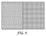
図3は、タッチセンサーの導電性バーを構成する連続的六角形金属メッシュ微小パターン(六角形メッシュを形成する2〜3μm幅の線状金属特徴で、ここにおいて六角形は直径300μmを有する)と、非連続的(すなわち点状の)微小パターン特徴(3μm×3μmの点が、10.2μm間隔の三角形配列になっている)とを有する、金属微小パターンの光学顕微鏡写真である。この非連続的点の配列は、第1四分割の「3M」図形にのみ存在した。一方、図形に隣接する対照領域(例えば第1四分割の周囲部分)は、連続的六角形金属メッシュ微小パターンのみを有し、非連続的(すなわち点状)微小パターン特徴は欠いていた。この点の寸法と間隔は、合計金属微小パターン密度11〜12%を有する3M図形をもたらし、一方で、この図形の外側にある対照領域の六角形金属メッシュ微小パターンは、合計金属微小パターン密度が1.3〜2%であった。この図形について、金属微小パターンのコントラスト比は約7であった。このロゴの内側と外側の陰影領域比率の差(すなわち、合計金属微小パターン密度の差)は約10%であった(11.3〜12%から1.3〜2%を差し引く)。

Claims (3)
- 金属微小パターンを有する透明基材を含む電子ディスプレイであって、該金属微小パターンの少なくとも一部分は連続的に、該電子ディスプレイの回路に電気的に接続しており、該金属微小パターンは、隣接する対照領域によって画定される少なくとも1つの図形を含み、該図形の該金属微小パターン、該対照領域の該金属微小パターン、又はこれらの組み合わせは、該電子ディスプレイの回路と電気的に接続されていない非連続的微小パターン特徴を含んでなる、電子ディスプレイ。
- 前記非連続的微小パターン特徴が、点、線分、塗り潰し図形、又はこれらの組み合わせの配列を含む、請求項1に記載の電子ディスプレイ。
- 前記基材が前記電子ディスプレイのタッチセンサーの一部である、請求項1又は2に記載の電子ディスプレイ。
Applications Claiming Priority (3)
| Application Number | Priority Date | Filing Date | Title |
|---|---|---|---|
| US22188809P | 2009-06-30 | 2009-06-30 | |
| US61/221,888 | 2009-06-30 | ||
| PCT/US2010/039103 WO2011002617A1 (en) | 2009-06-30 | 2010-06-18 | Electronic displays and metal micropatterned substrates having a graphic |
Publications (3)
| Publication Number | Publication Date |
|---|---|
| JP2012532336A JP2012532336A (ja) | 2012-12-13 |
| JP2012532336A5 JP2012532336A5 (ja) | 2013-08-08 |
| JP5747027B2 true JP5747027B2 (ja) | 2015-07-08 |
Family
ID=42732189
Family Applications (1)
| Application Number | Title | Priority Date | Filing Date |
|---|---|---|---|
| JP2012517591A Expired - Fee Related JP5747027B2 (ja) | 2009-06-30 | 2010-06-18 | 図形を有する電子ディスプレイ及び金属微小パターン化基材 |
Country Status (5)
| Country | Link |
|---|---|
| US (2) | US8553400B2 (ja) |
| EP (1) | EP2449547B1 (ja) |
| JP (1) | JP5747027B2 (ja) |
| CN (1) | CN102473370B (ja) |
| WO (1) | WO2011002617A1 (ja) |
Families Citing this family (21)
| Publication number | Priority date | Publication date | Assignee | Title |
|---|---|---|---|---|
| WO2010099132A2 (en) | 2009-02-26 | 2010-09-02 | 3M Innovative Properties Company | Touch screen sensor and patterned substrate having overlaid micropatterns with low visibility |
| US10620754B2 (en) | 2010-11-22 | 2020-04-14 | 3M Innovative Properties Company | Touch-sensitive device with electrodes having location pattern included therein |
| FR2968103B1 (fr) * | 2010-11-26 | 2013-04-26 | Stantum | Capteur tactile transparent et procédé de fabrication associe |
| KR20140030120A (ko) | 2010-12-16 | 2014-03-11 | 쓰리엠 이노베이티브 프로퍼티즈 컴파니 | 투명한 미세 패턴화된 rfid 안테나 및 이를 포함하는 물품 |
| KR20140009318A (ko) | 2011-02-02 | 2014-01-22 | 쓰리엠 이노베이티브 프로퍼티즈 컴파니 | 암화 다층 반도체 트레이스가 구비된 패턴닝된 기판 |
| US8933906B2 (en) | 2011-02-02 | 2015-01-13 | 3M Innovative Properties Company | Patterned substrates with non-linear conductor traces |
| US9523919B2 (en) | 2011-05-31 | 2016-12-20 | 3M Innovative Properties Company | Methods for making differentially pattern cured microstructured articles |
| JP5964953B2 (ja) | 2011-05-31 | 2016-08-03 | スリーエム イノベイティブ プロパティズ カンパニー | 非連続的なトポグラフィーを有する微細構造化ツールを作成するための方法、及びこれにより製造される物品 |
| CN103376958A (zh) * | 2012-04-19 | 2013-10-30 | 深圳欧菲光科技股份有限公司 | 电容感应组件、其制备方法及使用电容感应组件的触控屏 |
| WO2013180971A1 (en) * | 2012-05-30 | 2013-12-05 | Sipix Imaging, Inc. | Display device with watermark |
| US10401668B2 (en) | 2012-05-30 | 2019-09-03 | E Ink California, Llc | Display device with visually-distinguishable watermark area and non-watermark area |
| JP2015535950A (ja) * | 2012-09-20 | 2015-12-17 | コーニンクレッカ フィリップス エヌ ヴェKoninklijke Philips N.V. | 光学装置、レンズ、照明装置、システム及び方法 |
| US10720087B2 (en) | 2013-12-13 | 2020-07-21 | Bang & Olufsen A/S | Illuminated patterns on a surface |
| US9395765B2 (en) | 2014-07-31 | 2016-07-19 | Dell Products, Lp | Unibody construction triangular chassis |
| KR102253870B1 (ko) | 2014-08-11 | 2021-05-21 | 삼성디스플레이 주식회사 | 유기 발광 표시 장치 |
| JP6543550B2 (ja) * | 2015-10-01 | 2019-07-10 | 株式会社Vtsタッチセンサー | タッチパネル |
| US10274786B2 (en) * | 2016-06-09 | 2019-04-30 | Samsung Display Co., Ltd. | Liquid crystal display device and manufacturing method thereof |
| JP7271082B2 (ja) * | 2017-11-20 | 2023-05-11 | 大日本印刷株式会社 | タッチパネル、タッチパネル付き表示装置、加飾シート |
| JP2021036350A (ja) * | 2017-12-19 | 2021-03-04 | パナソニックIpマネジメント株式会社 | タッチセンサおよびそれを備えた入力装置 |
| US10673132B2 (en) * | 2018-05-22 | 2020-06-02 | Robert Joseph Kaminsky, JR. | Computer network routing device with decorative covering and method of distributing computer network routing devices |
| CN113463099B (zh) * | 2020-03-31 | 2023-08-29 | 长沙韶光铬版有限公司 | 一种银的细微图形化蚀刻方法 |
Family Cites Families (23)
| Publication number | Priority date | Publication date | Assignee | Title |
|---|---|---|---|---|
| JP2543709B2 (ja) * | 1987-07-13 | 1996-10-16 | セイコーエプソン株式会社 | 入力装置 |
| JP3516848B2 (ja) * | 1997-03-28 | 2004-04-05 | シャープ株式会社 | タッチパネル |
| US6977808B2 (en) | 1999-05-14 | 2005-12-20 | Apple Computer, Inc. | Display housing for computing device |
| FR2850482A1 (fr) * | 2003-01-29 | 2004-07-30 | Hubert Abitbol | Ecran-cache representant des objets virtuels 3d a placer devant un ecran plasma, lcd ou cathodique |
| AU2003227020A1 (en) * | 2003-02-27 | 2004-09-17 | Bang And Olufsen A/S | Metal structure with translucent region |
| JP4610416B2 (ja) | 2005-06-10 | 2011-01-12 | 日本写真印刷株式会社 | 静電容量型タッチパネル |
| US7947350B2 (en) * | 2005-08-26 | 2011-05-24 | Richard Lavosky | Film label and coating |
| DE102006005000B4 (de) * | 2006-02-01 | 2016-05-04 | Ovd Kinegram Ag | Mehrschichtkörper mit Mikrolinsen-Anordnung |
| US8764996B2 (en) | 2006-10-18 | 2014-07-01 | 3M Innovative Properties Company | Methods of patterning a material on polymeric substrates |
| JP2008124299A (ja) * | 2006-11-14 | 2008-05-29 | Toppan Printing Co Ltd | Emiシールド部材の製造方法及びemiシールド部材並びに画像表示装置 |
| JP2008129708A (ja) * | 2006-11-17 | 2008-06-05 | Alps Electric Co Ltd | 透明タッチパネル及びその製造方法 |
| JP4518097B2 (ja) * | 2007-04-13 | 2010-08-04 | ソニー株式会社 | 情報処理装置のフロント構造 |
| US7609451B1 (en) * | 2008-02-05 | 2009-10-27 | Serigraph, Inc. | Printed article for displaying images having improved definition and depth |
| US8425792B2 (en) | 2008-02-28 | 2013-04-23 | 3M Innovative Properties Company | Methods of patterning a conductor on a substrate |
| US8284332B2 (en) | 2008-08-01 | 2012-10-09 | 3M Innovative Properties Company | Touch screen sensor with low visibility conductors |
| EP4071785A1 (en) | 2008-02-28 | 2022-10-12 | 3M Innovative Properties Company | Touch screen sensor |
| EP2260366B1 (en) | 2008-02-28 | 2018-09-19 | 3M Innovative Properties Company | Touch screen sensor having varying sheet resistance |
| US7778015B2 (en) * | 2008-07-11 | 2010-08-17 | Apple Inc. | Microperforated and backlit displays having alternative display capabilities |
| US8726497B2 (en) | 2008-08-01 | 2014-05-20 | 3M Innovative Properties Company | Methods of making composite electrodes |
| EP2370269B1 (en) | 2008-12-11 | 2015-08-05 | 3M Innovative Properties Company | Patterning process |
| WO2010099132A2 (en) | 2009-02-26 | 2010-09-02 | 3M Innovative Properties Company | Touch screen sensor and patterned substrate having overlaid micropatterns with low visibility |
| CN102803562B (zh) | 2009-06-25 | 2015-09-30 | 3M创新有限公司 | 湿式蚀刻自组装单层图案化基材和金属图案化制品的方法 |
| US9579690B2 (en) * | 2010-05-20 | 2017-02-28 | Nokia Technologies Oy | Generating perceptible touch stimulus |
-
2010
- 2010-06-18 JP JP2012517591A patent/JP5747027B2/ja not_active Expired - Fee Related
- 2010-06-18 CN CN201080029255.0A patent/CN102473370B/zh not_active Expired - Fee Related
- 2010-06-18 EP EP10730630.0A patent/EP2449547B1/en not_active Not-in-force
- 2010-06-18 US US13/321,185 patent/US8553400B2/en active Active
- 2010-06-18 WO PCT/US2010/039103 patent/WO2011002617A1/en active Application Filing
-
2013
- 2013-09-05 US US14/018,475 patent/US9060434B2/en not_active Expired - Fee Related
Also Published As
| Publication number | Publication date |
|---|---|
| US8553400B2 (en) | 2013-10-08 |
| JP2012532336A (ja) | 2012-12-13 |
| EP2449547B1 (en) | 2016-09-21 |
| CN102473370A (zh) | 2012-05-23 |
| US20120086660A1 (en) | 2012-04-12 |
| CN102473370B (zh) | 2015-06-17 |
| US20140003005A1 (en) | 2014-01-02 |
| WO2011002617A1 (en) | 2011-01-06 |
| US9060434B2 (en) | 2015-06-16 |
| EP2449547A1 (en) | 2012-05-09 |
Similar Documents
| Publication | Publication Date | Title |
|---|---|---|
| JP5747027B2 (ja) | 図形を有する電子ディスプレイ及び金属微小パターン化基材 | |
| US8703232B2 (en) | Method of forming a microstructure | |
| JP6321716B2 (ja) | 基材上に導電体をパターン化する方法 | |
| EP2311301B1 (en) | Method of forming a patterned substrate | |
| KR20110127236A (ko) | 가시성이 낮은 오버레이된 미세패턴을 갖는 패턴화된 기판 및 터치 스크린 센서 | |
| WO2014038616A1 (ja) | 防汚体、表示装置、入力装置および電子機器 | |
| TW201418000A (zh) | 防污體、顯示裝置、輸入裝置、電子機器及防污性物品 | |
| JP2016510153A (ja) | 金属細線を含む透明基板及びその製造方法 | |
| CN101185384A (zh) | 透明导电膜及其制造方法 | |
| TWI711950B (zh) | 觸控面板感測器 | |
| KR100957487B1 (ko) | 플라스틱 전극필름 제조방법 | |
| WO2003045125A1 (fr) | Materiau de fenetre transmettant la lumiere et protege contre les ondes electromagnetiques et procede de fabrication de ce materiau | |
| JP4679088B2 (ja) | 透明面状発熱体及びその製造方法 | |
| GB2489974A (en) | Improvements in and relating to transparent electrical or electronic components | |
| EP3683809B1 (en) | Embedded-type transparent electrode substrate and method for manufacturing same | |
| JP6722291B2 (ja) | 導電性フィルム、タッチパネル、フォトマスク、インプリントテンプレート、導電性フィルム形成用積層体、導電性フィルムの製造方法、および電子デバイスの製造方法 | |
| JP2004288800A (ja) | 電磁波シールド材およびその製造方法 | |
| TWM328584U (en) | Window plate structure of display panel |
Legal Events
| Date | Code | Title | Description |
|---|---|---|---|
| A521 | Request for written amendment filed |
Free format text: JAPANESE INTERMEDIATE CODE: A523 Effective date: 20130617 |
|
| A621 | Written request for application examination |
Free format text: JAPANESE INTERMEDIATE CODE: A621 Effective date: 20130617 |
|
| A977 | Report on retrieval |
Free format text: JAPANESE INTERMEDIATE CODE: A971007 Effective date: 20140620 |
|
| A131 | Notification of reasons for refusal |
Free format text: JAPANESE INTERMEDIATE CODE: A131 Effective date: 20140729 |
|
| TRDD | Decision of grant or rejection written | ||
| A01 | Written decision to grant a patent or to grant a registration (utility model) |
Free format text: JAPANESE INTERMEDIATE CODE: A01 Effective date: 20150414 |
|
| A61 | First payment of annual fees (during grant procedure) |
Free format text: JAPANESE INTERMEDIATE CODE: A61 Effective date: 20150511 |
|
| R150 | Certificate of patent or registration of utility model |
Ref document number: 5747027 Country of ref document: JP Free format text: JAPANESE INTERMEDIATE CODE: R150 |
|
| LAPS | Cancellation because of no payment of annual fees |