JP5700927B2 - 半導体装置及び半導体装置の製造方法 - Google Patents
半導体装置及び半導体装置の製造方法 Download PDFInfo
- Publication number
- JP5700927B2 JP5700927B2 JP2009266485A JP2009266485A JP5700927B2 JP 5700927 B2 JP5700927 B2 JP 5700927B2 JP 2009266485 A JP2009266485 A JP 2009266485A JP 2009266485 A JP2009266485 A JP 2009266485A JP 5700927 B2 JP5700927 B2 JP 5700927B2
- Authority
- JP
- Japan
- Prior art keywords
- chip
- resin
- bonding wire
- sealing
- semiconductor chip
- Prior art date
- Legal status (The legal status is an assumption and is not a legal conclusion. Google has not performed a legal analysis and makes no representation as to the accuracy of the status listed.)
- Expired - Fee Related
Links
Images


Classifications
-
- H—ELECTRICITY
- H01—ELECTRIC ELEMENTS
- H01L—SEMICONDUCTOR DEVICES NOT COVERED BY CLASS H10
- H01L23/00—Details of semiconductor or other solid state devices
- H01L23/48—Arrangements for conducting electric current to or from the solid state body in operation, e.g. leads, terminal arrangements ; Selection of materials therefor
- H01L23/488—Arrangements for conducting electric current to or from the solid state body in operation, e.g. leads, terminal arrangements ; Selection of materials therefor consisting of soldered or bonded constructions
- H01L23/495—Lead-frames or other flat leads
- H01L23/49572—Lead-frames or other flat leads consisting of thin flexible metallic tape with or without a film carrier
-
- H—ELECTRICITY
- H01—ELECTRIC ELEMENTS
- H01L—SEMICONDUCTOR DEVICES NOT COVERED BY CLASS H10
- H01L21/00—Processes or apparatus adapted for the manufacture or treatment of semiconductor or solid state devices or of parts thereof
- H01L21/02—Manufacture or treatment of semiconductor devices or of parts thereof
- H01L21/04—Manufacture or treatment of semiconductor devices or of parts thereof the devices having at least one potential-jump barrier or surface barrier, e.g. PN junction, depletion layer or carrier concentration layer
- H01L21/50—Assembly of semiconductor devices using processes or apparatus not provided for in a single one of the subgroups H01L21/06 - H01L21/326, e.g. sealing of a cap to a base of a container
- H01L21/56—Encapsulations, e.g. encapsulation layers, coatings
- H01L21/568—Temporary substrate used as encapsulation process aid
-
- H—ELECTRICITY
- H01—ELECTRIC ELEMENTS
- H01L—SEMICONDUCTOR DEVICES NOT COVERED BY CLASS H10
- H01L23/00—Details of semiconductor or other solid state devices
- H01L23/28—Encapsulations, e.g. encapsulating layers, coatings, e.g. for protection
- H01L23/31—Encapsulations, e.g. encapsulating layers, coatings, e.g. for protection characterised by the arrangement or shape
- H01L23/3107—Encapsulations, e.g. encapsulating layers, coatings, e.g. for protection characterised by the arrangement or shape the device being completely enclosed
- H01L23/3121—Encapsulations, e.g. encapsulating layers, coatings, e.g. for protection characterised by the arrangement or shape the device being completely enclosed a substrate forming part of the encapsulation
-
- H—ELECTRICITY
- H01—ELECTRIC ELEMENTS
- H01L—SEMICONDUCTOR DEVICES NOT COVERED BY CLASS H10
- H01L23/00—Details of semiconductor or other solid state devices
- H01L23/48—Arrangements for conducting electric current to or from the solid state body in operation, e.g. leads, terminal arrangements ; Selection of materials therefor
- H01L23/488—Arrangements for conducting electric current to or from the solid state body in operation, e.g. leads, terminal arrangements ; Selection of materials therefor consisting of soldered or bonded constructions
- H01L23/495—Lead-frames or other flat leads
- H01L23/49541—Geometry of the lead-frame
- H01L23/49548—Cross section geometry
- H01L23/49551—Cross section geometry characterised by bent parts
- H01L23/49555—Cross section geometry characterised by bent parts the bent parts being the outer leads
-
- H—ELECTRICITY
- H01—ELECTRIC ELEMENTS
- H01L—SEMICONDUCTOR DEVICES NOT COVERED BY CLASS H10
- H01L24/00—Arrangements for connecting or disconnecting semiconductor or solid-state bodies; Methods or apparatus related thereto
- H01L24/01—Means for bonding being attached to, or being formed on, the surface to be connected, e.g. chip-to-package, die-attach, "first-level" interconnects; Manufacturing methods related thereto
- H01L24/18—High density interconnect [HDI] connectors; Manufacturing methods related thereto
- H01L24/23—Structure, shape, material or disposition of the high density interconnect connectors after the connecting process
- H01L24/24—Structure, shape, material or disposition of the high density interconnect connectors after the connecting process of an individual high density interconnect connector
-
- H—ELECTRICITY
- H01—ELECTRIC ELEMENTS
- H01L—SEMICONDUCTOR DEVICES NOT COVERED BY CLASS H10
- H01L24/00—Arrangements for connecting or disconnecting semiconductor or solid-state bodies; Methods or apparatus related thereto
- H01L24/01—Means for bonding being attached to, or being formed on, the surface to be connected, e.g. chip-to-package, die-attach, "first-level" interconnects; Manufacturing methods related thereto
- H01L24/42—Wire connectors; Manufacturing methods related thereto
- H01L24/47—Structure, shape, material or disposition of the wire connectors after the connecting process
- H01L24/48—Structure, shape, material or disposition of the wire connectors after the connecting process of an individual wire connector
-
- H—ELECTRICITY
- H01—ELECTRIC ELEMENTS
- H01L—SEMICONDUCTOR DEVICES NOT COVERED BY CLASS H10
- H01L24/00—Arrangements for connecting or disconnecting semiconductor or solid-state bodies; Methods or apparatus related thereto
- H01L24/80—Methods for connecting semiconductor or other solid state bodies using means for bonding being attached to, or being formed on, the surface to be connected
- H01L24/82—Methods for connecting semiconductor or other solid state bodies using means for bonding being attached to, or being formed on, the surface to be connected by forming build-up interconnects at chip-level, e.g. for high density interconnects [HDI]
-
- H—ELECTRICITY
- H01—ELECTRIC ELEMENTS
- H01L—SEMICONDUCTOR DEVICES NOT COVERED BY CLASS H10
- H01L24/00—Arrangements for connecting or disconnecting semiconductor or solid-state bodies; Methods or apparatus related thereto
- H01L24/91—Methods for connecting semiconductor or solid state bodies including different methods provided for in two or more of groups H01L24/80 - H01L24/90
-
- H—ELECTRICITY
- H01—ELECTRIC ELEMENTS
- H01L—SEMICONDUCTOR DEVICES NOT COVERED BY CLASS H10
- H01L24/00—Arrangements for connecting or disconnecting semiconductor or solid-state bodies; Methods or apparatus related thereto
- H01L24/93—Batch processes
- H01L24/95—Batch processes at chip-level, i.e. with connecting carried out on a plurality of singulated devices, i.e. on diced chips
- H01L24/97—Batch processes at chip-level, i.e. with connecting carried out on a plurality of singulated devices, i.e. on diced chips the devices being connected to a common substrate, e.g. interposer, said common substrate being separable into individual assemblies after connecting
-
- H—ELECTRICITY
- H01—ELECTRIC ELEMENTS
- H01L—SEMICONDUCTOR DEVICES NOT COVERED BY CLASS H10
- H01L25/00—Assemblies consisting of a plurality of individual semiconductor or other solid state devices ; Multistep manufacturing processes thereof
- H01L25/03—Assemblies consisting of a plurality of individual semiconductor or other solid state devices ; Multistep manufacturing processes thereof all the devices being of a type provided for in the same subgroup of groups H01L27/00 - H01L33/00, or in a single subclass of H10K, H10N, e.g. assemblies of rectifier diodes
- H01L25/04—Assemblies consisting of a plurality of individual semiconductor or other solid state devices ; Multistep manufacturing processes thereof all the devices being of a type provided for in the same subgroup of groups H01L27/00 - H01L33/00, or in a single subclass of H10K, H10N, e.g. assemblies of rectifier diodes the devices not having separate containers
- H01L25/065—Assemblies consisting of a plurality of individual semiconductor or other solid state devices ; Multistep manufacturing processes thereof all the devices being of a type provided for in the same subgroup of groups H01L27/00 - H01L33/00, or in a single subclass of H10K, H10N, e.g. assemblies of rectifier diodes the devices not having separate containers the devices being of a type provided for in group H01L27/00
- H01L25/0657—Stacked arrangements of devices
-
- H—ELECTRICITY
- H01—ELECTRIC ELEMENTS
- H01L—SEMICONDUCTOR DEVICES NOT COVERED BY CLASS H10
- H01L25/00—Assemblies consisting of a plurality of individual semiconductor or other solid state devices ; Multistep manufacturing processes thereof
- H01L25/50—Multistep manufacturing processes of assemblies consisting of devices, each device being of a type provided for in group H01L27/00 or H01L29/00
-
- H—ELECTRICITY
- H01—ELECTRIC ELEMENTS
- H01L—SEMICONDUCTOR DEVICES NOT COVERED BY CLASS H10
- H01L2224/00—Indexing scheme for arrangements for connecting or disconnecting semiconductor or solid-state bodies and methods related thereto as covered by H01L24/00
- H01L2224/01—Means for bonding being attached to, or being formed on, the surface to be connected, e.g. chip-to-package, die-attach, "first-level" interconnects; Manufacturing methods related thereto
- H01L2224/02—Bonding areas; Manufacturing methods related thereto
- H01L2224/023—Redistribution layers [RDL] for bonding areas
- H01L2224/0233—Structure of the redistribution layers
-
- H—ELECTRICITY
- H01—ELECTRIC ELEMENTS
- H01L—SEMICONDUCTOR DEVICES NOT COVERED BY CLASS H10
- H01L2224/00—Indexing scheme for arrangements for connecting or disconnecting semiconductor or solid-state bodies and methods related thereto as covered by H01L24/00
- H01L2224/01—Means for bonding being attached to, or being formed on, the surface to be connected, e.g. chip-to-package, die-attach, "first-level" interconnects; Manufacturing methods related thereto
- H01L2224/02—Bonding areas; Manufacturing methods related thereto
- H01L2224/023—Redistribution layers [RDL] for bonding areas
- H01L2224/0237—Disposition of the redistribution layers
- H01L2224/02371—Disposition of the redistribution layers connecting the bonding area on a surface of the semiconductor or solid-state body with another surface of the semiconductor or solid-state body
-
- H—ELECTRICITY
- H01—ELECTRIC ELEMENTS
- H01L—SEMICONDUCTOR DEVICES NOT COVERED BY CLASS H10
- H01L2224/00—Indexing scheme for arrangements for connecting or disconnecting semiconductor or solid-state bodies and methods related thereto as covered by H01L24/00
- H01L2224/01—Means for bonding being attached to, or being formed on, the surface to be connected, e.g. chip-to-package, die-attach, "first-level" interconnects; Manufacturing methods related thereto
- H01L2224/02—Bonding areas; Manufacturing methods related thereto
- H01L2224/04—Structure, shape, material or disposition of the bonding areas prior to the connecting process
- H01L2224/04105—Bonding areas formed on an encapsulation of the semiconductor or solid-state body, e.g. bonding areas on chip-scale packages
-
- H—ELECTRICITY
- H01—ELECTRIC ELEMENTS
- H01L—SEMICONDUCTOR DEVICES NOT COVERED BY CLASS H10
- H01L2224/00—Indexing scheme for arrangements for connecting or disconnecting semiconductor or solid-state bodies and methods related thereto as covered by H01L24/00
- H01L2224/01—Means for bonding being attached to, or being formed on, the surface to be connected, e.g. chip-to-package, die-attach, "first-level" interconnects; Manufacturing methods related thereto
- H01L2224/18—High density interconnect [HDI] connectors; Manufacturing methods related thereto
- H01L2224/23—Structure, shape, material or disposition of the high density interconnect connectors after the connecting process
- H01L2224/24—Structure, shape, material or disposition of the high density interconnect connectors after the connecting process of an individual high density interconnect connector
- H01L2224/241—Disposition
- H01L2224/24135—Connecting between different semiconductor or solid-state bodies, i.e. chip-to-chip
- H01L2224/24145—Connecting between different semiconductor or solid-state bodies, i.e. chip-to-chip the bodies being stacked
-
- H—ELECTRICITY
- H01—ELECTRIC ELEMENTS
- H01L—SEMICONDUCTOR DEVICES NOT COVERED BY CLASS H10
- H01L2224/00—Indexing scheme for arrangements for connecting or disconnecting semiconductor or solid-state bodies and methods related thereto as covered by H01L24/00
- H01L2224/01—Means for bonding being attached to, or being formed on, the surface to be connected, e.g. chip-to-package, die-attach, "first-level" interconnects; Manufacturing methods related thereto
- H01L2224/26—Layer connectors, e.g. plate connectors, solder or adhesive layers; Manufacturing methods related thereto
- H01L2224/31—Structure, shape, material or disposition of the layer connectors after the connecting process
- H01L2224/32—Structure, shape, material or disposition of the layer connectors after the connecting process of an individual layer connector
- H01L2224/321—Disposition
- H01L2224/32135—Disposition the layer connector connecting between different semiconductor or solid-state bodies, i.e. chip-to-chip
- H01L2224/32145—Disposition the layer connector connecting between different semiconductor or solid-state bodies, i.e. chip-to-chip the bodies being stacked
-
- H—ELECTRICITY
- H01—ELECTRIC ELEMENTS
- H01L—SEMICONDUCTOR DEVICES NOT COVERED BY CLASS H10
- H01L2224/00—Indexing scheme for arrangements for connecting or disconnecting semiconductor or solid-state bodies and methods related thereto as covered by H01L24/00
- H01L2224/01—Means for bonding being attached to, or being formed on, the surface to be connected, e.g. chip-to-package, die-attach, "first-level" interconnects; Manufacturing methods related thereto
- H01L2224/26—Layer connectors, e.g. plate connectors, solder or adhesive layers; Manufacturing methods related thereto
- H01L2224/31—Structure, shape, material or disposition of the layer connectors after the connecting process
- H01L2224/32—Structure, shape, material or disposition of the layer connectors after the connecting process of an individual layer connector
- H01L2224/321—Disposition
- H01L2224/32151—Disposition the layer connector connecting between a semiconductor or solid-state body and an item not being a semiconductor or solid-state body, e.g. chip-to-substrate, chip-to-passive
- H01L2224/32221—Disposition the layer connector connecting between a semiconductor or solid-state body and an item not being a semiconductor or solid-state body, e.g. chip-to-substrate, chip-to-passive the body and the item being stacked
- H01L2224/32225—Disposition the layer connector connecting between a semiconductor or solid-state body and an item not being a semiconductor or solid-state body, e.g. chip-to-substrate, chip-to-passive the body and the item being stacked the item being non-metallic, e.g. insulating substrate with or without metallisation
-
- H—ELECTRICITY
- H01—ELECTRIC ELEMENTS
- H01L—SEMICONDUCTOR DEVICES NOT COVERED BY CLASS H10
- H01L2224/00—Indexing scheme for arrangements for connecting or disconnecting semiconductor or solid-state bodies and methods related thereto as covered by H01L24/00
- H01L2224/01—Means for bonding being attached to, or being formed on, the surface to be connected, e.g. chip-to-package, die-attach, "first-level" interconnects; Manufacturing methods related thereto
- H01L2224/42—Wire connectors; Manufacturing methods related thereto
- H01L2224/44—Structure, shape, material or disposition of the wire connectors prior to the connecting process
- H01L2224/45—Structure, shape, material or disposition of the wire connectors prior to the connecting process of an individual wire connector
- H01L2224/45001—Core members of the connector
- H01L2224/4501—Shape
- H01L2224/45012—Cross-sectional shape
- H01L2224/45014—Ribbon connectors, e.g. rectangular cross-section
-
- H—ELECTRICITY
- H01—ELECTRIC ELEMENTS
- H01L—SEMICONDUCTOR DEVICES NOT COVERED BY CLASS H10
- H01L2224/00—Indexing scheme for arrangements for connecting or disconnecting semiconductor or solid-state bodies and methods related thereto as covered by H01L24/00
- H01L2224/01—Means for bonding being attached to, or being formed on, the surface to be connected, e.g. chip-to-package, die-attach, "first-level" interconnects; Manufacturing methods related thereto
- H01L2224/42—Wire connectors; Manufacturing methods related thereto
- H01L2224/44—Structure, shape, material or disposition of the wire connectors prior to the connecting process
- H01L2224/45—Structure, shape, material or disposition of the wire connectors prior to the connecting process of an individual wire connector
- H01L2224/45001—Core members of the connector
- H01L2224/4501—Shape
- H01L2224/45012—Cross-sectional shape
- H01L2224/45015—Cross-sectional shape being circular
-
- H—ELECTRICITY
- H01—ELECTRIC ELEMENTS
- H01L—SEMICONDUCTOR DEVICES NOT COVERED BY CLASS H10
- H01L2224/00—Indexing scheme for arrangements for connecting or disconnecting semiconductor or solid-state bodies and methods related thereto as covered by H01L24/00
- H01L2224/01—Means for bonding being attached to, or being formed on, the surface to be connected, e.g. chip-to-package, die-attach, "first-level" interconnects; Manufacturing methods related thereto
- H01L2224/42—Wire connectors; Manufacturing methods related thereto
- H01L2224/44—Structure, shape, material or disposition of the wire connectors prior to the connecting process
- H01L2224/45—Structure, shape, material or disposition of the wire connectors prior to the connecting process of an individual wire connector
- H01L2224/45001—Core members of the connector
- H01L2224/45099—Material
- H01L2224/451—Material with a principal constituent of the material being a metal or a metalloid, e.g. boron (B), silicon (Si), germanium (Ge), arsenic (As), antimony (Sb), tellurium (Te) and polonium (Po), and alloys thereof
- H01L2224/45117—Material with a principal constituent of the material being a metal or a metalloid, e.g. boron (B), silicon (Si), germanium (Ge), arsenic (As), antimony (Sb), tellurium (Te) and polonium (Po), and alloys thereof the principal constituent melting at a temperature of greater than or equal to 400°C and less than 950°C
- H01L2224/45124—Aluminium (Al) as principal constituent
-
- H—ELECTRICITY
- H01—ELECTRIC ELEMENTS
- H01L—SEMICONDUCTOR DEVICES NOT COVERED BY CLASS H10
- H01L2224/00—Indexing scheme for arrangements for connecting or disconnecting semiconductor or solid-state bodies and methods related thereto as covered by H01L24/00
- H01L2224/01—Means for bonding being attached to, or being formed on, the surface to be connected, e.g. chip-to-package, die-attach, "first-level" interconnects; Manufacturing methods related thereto
- H01L2224/42—Wire connectors; Manufacturing methods related thereto
- H01L2224/44—Structure, shape, material or disposition of the wire connectors prior to the connecting process
- H01L2224/45—Structure, shape, material or disposition of the wire connectors prior to the connecting process of an individual wire connector
- H01L2224/45001—Core members of the connector
- H01L2224/45099—Material
- H01L2224/451—Material with a principal constituent of the material being a metal or a metalloid, e.g. boron (B), silicon (Si), germanium (Ge), arsenic (As), antimony (Sb), tellurium (Te) and polonium (Po), and alloys thereof
- H01L2224/45138—Material with a principal constituent of the material being a metal or a metalloid, e.g. boron (B), silicon (Si), germanium (Ge), arsenic (As), antimony (Sb), tellurium (Te) and polonium (Po), and alloys thereof the principal constituent melting at a temperature of greater than or equal to 950°C and less than 1550°C
- H01L2224/45144—Gold (Au) as principal constituent
-
- H—ELECTRICITY
- H01—ELECTRIC ELEMENTS
- H01L—SEMICONDUCTOR DEVICES NOT COVERED BY CLASS H10
- H01L2224/00—Indexing scheme for arrangements for connecting or disconnecting semiconductor or solid-state bodies and methods related thereto as covered by H01L24/00
- H01L2224/01—Means for bonding being attached to, or being formed on, the surface to be connected, e.g. chip-to-package, die-attach, "first-level" interconnects; Manufacturing methods related thereto
- H01L2224/42—Wire connectors; Manufacturing methods related thereto
- H01L2224/44—Structure, shape, material or disposition of the wire connectors prior to the connecting process
- H01L2224/45—Structure, shape, material or disposition of the wire connectors prior to the connecting process of an individual wire connector
- H01L2224/45001—Core members of the connector
- H01L2224/45099—Material
- H01L2224/451—Material with a principal constituent of the material being a metal or a metalloid, e.g. boron (B), silicon (Si), germanium (Ge), arsenic (As), antimony (Sb), tellurium (Te) and polonium (Po), and alloys thereof
- H01L2224/45138—Material with a principal constituent of the material being a metal or a metalloid, e.g. boron (B), silicon (Si), germanium (Ge), arsenic (As), antimony (Sb), tellurium (Te) and polonium (Po), and alloys thereof the principal constituent melting at a temperature of greater than or equal to 950°C and less than 1550°C
- H01L2224/45147—Copper (Cu) as principal constituent
-
- H—ELECTRICITY
- H01—ELECTRIC ELEMENTS
- H01L—SEMICONDUCTOR DEVICES NOT COVERED BY CLASS H10
- H01L2224/00—Indexing scheme for arrangements for connecting or disconnecting semiconductor or solid-state bodies and methods related thereto as covered by H01L24/00
- H01L2224/01—Means for bonding being attached to, or being formed on, the surface to be connected, e.g. chip-to-package, die-attach, "first-level" interconnects; Manufacturing methods related thereto
- H01L2224/42—Wire connectors; Manufacturing methods related thereto
- H01L2224/44—Structure, shape, material or disposition of the wire connectors prior to the connecting process
- H01L2224/45—Structure, shape, material or disposition of the wire connectors prior to the connecting process of an individual wire connector
- H01L2224/45001—Core members of the connector
- H01L2224/45099—Material
- H01L2224/451—Material with a principal constituent of the material being a metal or a metalloid, e.g. boron (B), silicon (Si), germanium (Ge), arsenic (As), antimony (Sb), tellurium (Te) and polonium (Po), and alloys thereof
- H01L2224/45163—Material with a principal constituent of the material being a metal or a metalloid, e.g. boron (B), silicon (Si), germanium (Ge), arsenic (As), antimony (Sb), tellurium (Te) and polonium (Po), and alloys thereof the principal constituent melting at a temperature of greater than 1550°C
- H01L2224/45184—Tungsten (W) as principal constituent
-
- H—ELECTRICITY
- H01—ELECTRIC ELEMENTS
- H01L—SEMICONDUCTOR DEVICES NOT COVERED BY CLASS H10
- H01L2224/00—Indexing scheme for arrangements for connecting or disconnecting semiconductor or solid-state bodies and methods related thereto as covered by H01L24/00
- H01L2224/01—Means for bonding being attached to, or being formed on, the surface to be connected, e.g. chip-to-package, die-attach, "first-level" interconnects; Manufacturing methods related thereto
- H01L2224/42—Wire connectors; Manufacturing methods related thereto
- H01L2224/44—Structure, shape, material or disposition of the wire connectors prior to the connecting process
- H01L2224/45—Structure, shape, material or disposition of the wire connectors prior to the connecting process of an individual wire connector
- H01L2224/4554—Coating
- H01L2224/45599—Material
- H01L2224/456—Material with a principal constituent of the material being a metal or a metalloid, e.g. boron (B), silicon (Si), germanium (Ge), arsenic (As), antimony (Sb), tellurium (Te) and polonium (Po), and alloys thereof
- H01L2224/45663—Material with a principal constituent of the material being a metal or a metalloid, e.g. boron (B), silicon (Si), germanium (Ge), arsenic (As), antimony (Sb), tellurium (Te) and polonium (Po), and alloys thereof the principal constituent melting at a temperature of greater than 1550°C
- H01L2224/45684—Tungsten (W) as principal constituent
-
- H—ELECTRICITY
- H01—ELECTRIC ELEMENTS
- H01L—SEMICONDUCTOR DEVICES NOT COVERED BY CLASS H10
- H01L2224/00—Indexing scheme for arrangements for connecting or disconnecting semiconductor or solid-state bodies and methods related thereto as covered by H01L24/00
- H01L2224/01—Means for bonding being attached to, or being formed on, the surface to be connected, e.g. chip-to-package, die-attach, "first-level" interconnects; Manufacturing methods related thereto
- H01L2224/42—Wire connectors; Manufacturing methods related thereto
- H01L2224/47—Structure, shape, material or disposition of the wire connectors after the connecting process
- H01L2224/48—Structure, shape, material or disposition of the wire connectors after the connecting process of an individual wire connector
- H01L2224/4805—Shape
- H01L2224/4809—Loop shape
- H01L2224/48091—Arched
-
- H—ELECTRICITY
- H01—ELECTRIC ELEMENTS
- H01L—SEMICONDUCTOR DEVICES NOT COVERED BY CLASS H10
- H01L2224/00—Indexing scheme for arrangements for connecting or disconnecting semiconductor or solid-state bodies and methods related thereto as covered by H01L24/00
- H01L2224/01—Means for bonding being attached to, or being formed on, the surface to be connected, e.g. chip-to-package, die-attach, "first-level" interconnects; Manufacturing methods related thereto
- H01L2224/42—Wire connectors; Manufacturing methods related thereto
- H01L2224/47—Structure, shape, material or disposition of the wire connectors after the connecting process
- H01L2224/48—Structure, shape, material or disposition of the wire connectors after the connecting process of an individual wire connector
- H01L2224/481—Disposition
- H01L2224/48135—Connecting between different semiconductor or solid-state bodies, i.e. chip-to-chip
- H01L2224/48145—Connecting between different semiconductor or solid-state bodies, i.e. chip-to-chip the bodies being stacked
- H01L2224/48147—Connecting between different semiconductor or solid-state bodies, i.e. chip-to-chip the bodies being stacked with an intermediate bond, e.g. continuous wire daisy chain
-
- H—ELECTRICITY
- H01—ELECTRIC ELEMENTS
- H01L—SEMICONDUCTOR DEVICES NOT COVERED BY CLASS H10
- H01L2224/00—Indexing scheme for arrangements for connecting or disconnecting semiconductor or solid-state bodies and methods related thereto as covered by H01L24/00
- H01L2224/01—Means for bonding being attached to, or being formed on, the surface to be connected, e.g. chip-to-package, die-attach, "first-level" interconnects; Manufacturing methods related thereto
- H01L2224/42—Wire connectors; Manufacturing methods related thereto
- H01L2224/47—Structure, shape, material or disposition of the wire connectors after the connecting process
- H01L2224/48—Structure, shape, material or disposition of the wire connectors after the connecting process of an individual wire connector
- H01L2224/481—Disposition
- H01L2224/48151—Connecting between a semiconductor or solid-state body and an item not being a semiconductor or solid-state body, e.g. chip-to-substrate, chip-to-passive
- H01L2224/48221—Connecting between a semiconductor or solid-state body and an item not being a semiconductor or solid-state body, e.g. chip-to-substrate, chip-to-passive the body and the item being stacked
- H01L2224/48225—Connecting between a semiconductor or solid-state body and an item not being a semiconductor or solid-state body, e.g. chip-to-substrate, chip-to-passive the body and the item being stacked the item being non-metallic, e.g. insulating substrate with or without metallisation
- H01L2224/48227—Connecting between a semiconductor or solid-state body and an item not being a semiconductor or solid-state body, e.g. chip-to-substrate, chip-to-passive the body and the item being stacked the item being non-metallic, e.g. insulating substrate with or without metallisation connecting the wire to a bond pad of the item
-
- H—ELECTRICITY
- H01—ELECTRIC ELEMENTS
- H01L—SEMICONDUCTOR DEVICES NOT COVERED BY CLASS H10
- H01L2224/00—Indexing scheme for arrangements for connecting or disconnecting semiconductor or solid-state bodies and methods related thereto as covered by H01L24/00
- H01L2224/01—Means for bonding being attached to, or being formed on, the surface to be connected, e.g. chip-to-package, die-attach, "first-level" interconnects; Manufacturing methods related thereto
- H01L2224/42—Wire connectors; Manufacturing methods related thereto
- H01L2224/47—Structure, shape, material or disposition of the wire connectors after the connecting process
- H01L2224/48—Structure, shape, material or disposition of the wire connectors after the connecting process of an individual wire connector
- H01L2224/484—Connecting portions
- H01L2224/4847—Connecting portions the connecting portion on the bonding area of the semiconductor or solid-state body being a wedge bond
- H01L2224/48472—Connecting portions the connecting portion on the bonding area of the semiconductor or solid-state body being a wedge bond the other connecting portion not on the bonding area also being a wedge bond, i.e. wedge-to-wedge
-
- H—ELECTRICITY
- H01—ELECTRIC ELEMENTS
- H01L—SEMICONDUCTOR DEVICES NOT COVERED BY CLASS H10
- H01L2224/00—Indexing scheme for arrangements for connecting or disconnecting semiconductor or solid-state bodies and methods related thereto as covered by H01L24/00
- H01L2224/01—Means for bonding being attached to, or being formed on, the surface to be connected, e.g. chip-to-package, die-attach, "first-level" interconnects; Manufacturing methods related thereto
- H01L2224/42—Wire connectors; Manufacturing methods related thereto
- H01L2224/47—Structure, shape, material or disposition of the wire connectors after the connecting process
- H01L2224/48—Structure, shape, material or disposition of the wire connectors after the connecting process of an individual wire connector
- H01L2224/485—Material
- H01L2224/48505—Material at the bonding interface
- H01L2224/48599—Principal constituent of the connecting portion of the wire connector being Gold (Au)
-
- H—ELECTRICITY
- H01—ELECTRIC ELEMENTS
- H01L—SEMICONDUCTOR DEVICES NOT COVERED BY CLASS H10
- H01L2224/00—Indexing scheme for arrangements for connecting or disconnecting semiconductor or solid-state bodies and methods related thereto as covered by H01L24/00
- H01L2224/01—Means for bonding being attached to, or being formed on, the surface to be connected, e.g. chip-to-package, die-attach, "first-level" interconnects; Manufacturing methods related thereto
- H01L2224/42—Wire connectors; Manufacturing methods related thereto
- H01L2224/47—Structure, shape, material or disposition of the wire connectors after the connecting process
- H01L2224/48—Structure, shape, material or disposition of the wire connectors after the connecting process of an individual wire connector
- H01L2224/485—Material
- H01L2224/48505—Material at the bonding interface
- H01L2224/48699—Principal constituent of the connecting portion of the wire connector being Aluminium (Al)
-
- H—ELECTRICITY
- H01—ELECTRIC ELEMENTS
- H01L—SEMICONDUCTOR DEVICES NOT COVERED BY CLASS H10
- H01L2224/00—Indexing scheme for arrangements for connecting or disconnecting semiconductor or solid-state bodies and methods related thereto as covered by H01L24/00
- H01L2224/01—Means for bonding being attached to, or being formed on, the surface to be connected, e.g. chip-to-package, die-attach, "first-level" interconnects; Manufacturing methods related thereto
- H01L2224/42—Wire connectors; Manufacturing methods related thereto
- H01L2224/47—Structure, shape, material or disposition of the wire connectors after the connecting process
- H01L2224/49—Structure, shape, material or disposition of the wire connectors after the connecting process of a plurality of wire connectors
- H01L2224/491—Disposition
- H01L2224/4911—Disposition the connectors being bonded to at least one common bonding area, e.g. daisy chain
-
- H—ELECTRICITY
- H01—ELECTRIC ELEMENTS
- H01L—SEMICONDUCTOR DEVICES NOT COVERED BY CLASS H10
- H01L2224/00—Indexing scheme for arrangements for connecting or disconnecting semiconductor or solid-state bodies and methods related thereto as covered by H01L24/00
- H01L2224/73—Means for bonding being of different types provided for in two or more of groups H01L2224/10, H01L2224/18, H01L2224/26, H01L2224/34, H01L2224/42, H01L2224/50, H01L2224/63, H01L2224/71
- H01L2224/732—Location after the connecting process
- H01L2224/73251—Location after the connecting process on different surfaces
- H01L2224/73265—Layer and wire connectors
-
- H—ELECTRICITY
- H01—ELECTRIC ELEMENTS
- H01L—SEMICONDUCTOR DEVICES NOT COVERED BY CLASS H10
- H01L2224/00—Indexing scheme for arrangements for connecting or disconnecting semiconductor or solid-state bodies and methods related thereto as covered by H01L24/00
- H01L2224/93—Batch processes
- H01L2224/95—Batch processes at chip-level, i.e. with connecting carried out on a plurality of singulated devices, i.e. on diced chips
- H01L2224/97—Batch processes at chip-level, i.e. with connecting carried out on a plurality of singulated devices, i.e. on diced chips the devices being connected to a common substrate, e.g. interposer, said common substrate being separable into individual assemblies after connecting
-
- H—ELECTRICITY
- H01—ELECTRIC ELEMENTS
- H01L—SEMICONDUCTOR DEVICES NOT COVERED BY CLASS H10
- H01L2225/00—Details relating to assemblies covered by the group H01L25/00 but not provided for in its subgroups
- H01L2225/03—All the devices being of a type provided for in the same subgroup of groups H01L27/00 - H01L33/648 and H10K99/00
- H01L2225/04—All the devices being of a type provided for in the same subgroup of groups H01L27/00 - H01L33/648 and H10K99/00 the devices not having separate containers
- H01L2225/065—All the devices being of a type provided for in the same subgroup of groups H01L27/00 - H01L33/648 and H10K99/00 the devices not having separate containers the devices being of a type provided for in group H01L27/00
- H01L2225/06503—Stacked arrangements of devices
- H01L2225/06506—Wire or wire-like electrical connections between devices
-
- H—ELECTRICITY
- H01—ELECTRIC ELEMENTS
- H01L—SEMICONDUCTOR DEVICES NOT COVERED BY CLASS H10
- H01L2225/00—Details relating to assemblies covered by the group H01L25/00 but not provided for in its subgroups
- H01L2225/03—All the devices being of a type provided for in the same subgroup of groups H01L27/00 - H01L33/648 and H10K99/00
- H01L2225/04—All the devices being of a type provided for in the same subgroup of groups H01L27/00 - H01L33/648 and H10K99/00 the devices not having separate containers
- H01L2225/065—All the devices being of a type provided for in the same subgroup of groups H01L27/00 - H01L33/648 and H10K99/00 the devices not having separate containers the devices being of a type provided for in group H01L27/00
- H01L2225/06503—Stacked arrangements of devices
- H01L2225/0651—Wire or wire-like electrical connections from device to substrate
-
- H—ELECTRICITY
- H01—ELECTRIC ELEMENTS
- H01L—SEMICONDUCTOR DEVICES NOT COVERED BY CLASS H10
- H01L2225/00—Details relating to assemblies covered by the group H01L25/00 but not provided for in its subgroups
- H01L2225/03—All the devices being of a type provided for in the same subgroup of groups H01L27/00 - H01L33/648 and H10K99/00
- H01L2225/04—All the devices being of a type provided for in the same subgroup of groups H01L27/00 - H01L33/648 and H10K99/00 the devices not having separate containers
- H01L2225/065—All the devices being of a type provided for in the same subgroup of groups H01L27/00 - H01L33/648 and H10K99/00 the devices not having separate containers the devices being of a type provided for in group H01L27/00
- H01L2225/06503—Stacked arrangements of devices
- H01L2225/06517—Bump or bump-like direct electrical connections from device to substrate
-
- H—ELECTRICITY
- H01—ELECTRIC ELEMENTS
- H01L—SEMICONDUCTOR DEVICES NOT COVERED BY CLASS H10
- H01L2225/00—Details relating to assemblies covered by the group H01L25/00 but not provided for in its subgroups
- H01L2225/03—All the devices being of a type provided for in the same subgroup of groups H01L27/00 - H01L33/648 and H10K99/00
- H01L2225/04—All the devices being of a type provided for in the same subgroup of groups H01L27/00 - H01L33/648 and H10K99/00 the devices not having separate containers
- H01L2225/065—All the devices being of a type provided for in the same subgroup of groups H01L27/00 - H01L33/648 and H10K99/00 the devices not having separate containers the devices being of a type provided for in group H01L27/00
- H01L2225/06503—Stacked arrangements of devices
- H01L2225/06551—Conductive connections on the side of the device
-
- H—ELECTRICITY
- H01—ELECTRIC ELEMENTS
- H01L—SEMICONDUCTOR DEVICES NOT COVERED BY CLASS H10
- H01L2225/00—Details relating to assemblies covered by the group H01L25/00 but not provided for in its subgroups
- H01L2225/03—All the devices being of a type provided for in the same subgroup of groups H01L27/00 - H01L33/648 and H10K99/00
- H01L2225/04—All the devices being of a type provided for in the same subgroup of groups H01L27/00 - H01L33/648 and H10K99/00 the devices not having separate containers
- H01L2225/065—All the devices being of a type provided for in the same subgroup of groups H01L27/00 - H01L33/648 and H10K99/00 the devices not having separate containers the devices being of a type provided for in group H01L27/00
- H01L2225/06503—Stacked arrangements of devices
- H01L2225/06555—Geometry of the stack, e.g. form of the devices, geometry to facilitate stacking
- H01L2225/06562—Geometry of the stack, e.g. form of the devices, geometry to facilitate stacking at least one device in the stack being rotated or offset
-
- H—ELECTRICITY
- H01—ELECTRIC ELEMENTS
- H01L—SEMICONDUCTOR DEVICES NOT COVERED BY CLASS H10
- H01L24/00—Arrangements for connecting or disconnecting semiconductor or solid-state bodies; Methods or apparatus related thereto
- H01L24/01—Means for bonding being attached to, or being formed on, the surface to be connected, e.g. chip-to-package, die-attach, "first-level" interconnects; Manufacturing methods related thereto
- H01L24/42—Wire connectors; Manufacturing methods related thereto
- H01L24/44—Structure, shape, material or disposition of the wire connectors prior to the connecting process
- H01L24/45—Structure, shape, material or disposition of the wire connectors prior to the connecting process of an individual wire connector
-
- H—ELECTRICITY
- H01—ELECTRIC ELEMENTS
- H01L—SEMICONDUCTOR DEVICES NOT COVERED BY CLASS H10
- H01L24/00—Arrangements for connecting or disconnecting semiconductor or solid-state bodies; Methods or apparatus related thereto
- H01L24/01—Means for bonding being attached to, or being formed on, the surface to be connected, e.g. chip-to-package, die-attach, "first-level" interconnects; Manufacturing methods related thereto
- H01L24/42—Wire connectors; Manufacturing methods related thereto
- H01L24/47—Structure, shape, material or disposition of the wire connectors after the connecting process
- H01L24/49—Structure, shape, material or disposition of the wire connectors after the connecting process of a plurality of wire connectors
-
- H—ELECTRICITY
- H01—ELECTRIC ELEMENTS
- H01L—SEMICONDUCTOR DEVICES NOT COVERED BY CLASS H10
- H01L24/00—Arrangements for connecting or disconnecting semiconductor or solid-state bodies; Methods or apparatus related thereto
- H01L24/73—Means for bonding being of different types provided for in two or more of groups H01L24/10, H01L24/18, H01L24/26, H01L24/34, H01L24/42, H01L24/50, H01L24/63, H01L24/71
-
- H—ELECTRICITY
- H01—ELECTRIC ELEMENTS
- H01L—SEMICONDUCTOR DEVICES NOT COVERED BY CLASS H10
- H01L2924/00—Indexing scheme for arrangements or methods for connecting or disconnecting semiconductor or solid-state bodies as covered by H01L24/00
- H01L2924/0001—Technical content checked by a classifier
- H01L2924/00014—Technical content checked by a classifier the subject-matter covered by the group, the symbol of which is combined with the symbol of this group, being disclosed without further technical details
-
- H—ELECTRICITY
- H01—ELECTRIC ELEMENTS
- H01L—SEMICONDUCTOR DEVICES NOT COVERED BY CLASS H10
- H01L2924/00—Indexing scheme for arrangements or methods for connecting or disconnecting semiconductor or solid-state bodies as covered by H01L24/00
- H01L2924/01—Chemical elements
- H01L2924/01005—Boron [B]
-
- H—ELECTRICITY
- H01—ELECTRIC ELEMENTS
- H01L—SEMICONDUCTOR DEVICES NOT COVERED BY CLASS H10
- H01L2924/00—Indexing scheme for arrangements or methods for connecting or disconnecting semiconductor or solid-state bodies as covered by H01L24/00
- H01L2924/01—Chemical elements
- H01L2924/01006—Carbon [C]
-
- H—ELECTRICITY
- H01—ELECTRIC ELEMENTS
- H01L—SEMICONDUCTOR DEVICES NOT COVERED BY CLASS H10
- H01L2924/00—Indexing scheme for arrangements or methods for connecting or disconnecting semiconductor or solid-state bodies as covered by H01L24/00
- H01L2924/01—Chemical elements
- H01L2924/01013—Aluminum [Al]
-
- H—ELECTRICITY
- H01—ELECTRIC ELEMENTS
- H01L—SEMICONDUCTOR DEVICES NOT COVERED BY CLASS H10
- H01L2924/00—Indexing scheme for arrangements or methods for connecting or disconnecting semiconductor or solid-state bodies as covered by H01L24/00
- H01L2924/01—Chemical elements
- H01L2924/01014—Silicon [Si]
-
- H—ELECTRICITY
- H01—ELECTRIC ELEMENTS
- H01L—SEMICONDUCTOR DEVICES NOT COVERED BY CLASS H10
- H01L2924/00—Indexing scheme for arrangements or methods for connecting or disconnecting semiconductor or solid-state bodies as covered by H01L24/00
- H01L2924/01—Chemical elements
- H01L2924/01019—Potassium [K]
-
- H—ELECTRICITY
- H01—ELECTRIC ELEMENTS
- H01L—SEMICONDUCTOR DEVICES NOT COVERED BY CLASS H10
- H01L2924/00—Indexing scheme for arrangements or methods for connecting or disconnecting semiconductor or solid-state bodies as covered by H01L24/00
- H01L2924/01—Chemical elements
- H01L2924/01027—Cobalt [Co]
-
- H—ELECTRICITY
- H01—ELECTRIC ELEMENTS
- H01L—SEMICONDUCTOR DEVICES NOT COVERED BY CLASS H10
- H01L2924/00—Indexing scheme for arrangements or methods for connecting or disconnecting semiconductor or solid-state bodies as covered by H01L24/00
- H01L2924/01—Chemical elements
- H01L2924/01029—Copper [Cu]
-
- H—ELECTRICITY
- H01—ELECTRIC ELEMENTS
- H01L—SEMICONDUCTOR DEVICES NOT COVERED BY CLASS H10
- H01L2924/00—Indexing scheme for arrangements or methods for connecting or disconnecting semiconductor or solid-state bodies as covered by H01L24/00
- H01L2924/01—Chemical elements
- H01L2924/01033—Arsenic [As]
-
- H—ELECTRICITY
- H01—ELECTRIC ELEMENTS
- H01L—SEMICONDUCTOR DEVICES NOT COVERED BY CLASS H10
- H01L2924/00—Indexing scheme for arrangements or methods for connecting or disconnecting semiconductor or solid-state bodies as covered by H01L24/00
- H01L2924/01—Chemical elements
- H01L2924/01047—Silver [Ag]
-
- H—ELECTRICITY
- H01—ELECTRIC ELEMENTS
- H01L—SEMICONDUCTOR DEVICES NOT COVERED BY CLASS H10
- H01L2924/00—Indexing scheme for arrangements or methods for connecting or disconnecting semiconductor or solid-state bodies as covered by H01L24/00
- H01L2924/01—Chemical elements
- H01L2924/0105—Tin [Sn]
-
- H—ELECTRICITY
- H01—ELECTRIC ELEMENTS
- H01L—SEMICONDUCTOR DEVICES NOT COVERED BY CLASS H10
- H01L2924/00—Indexing scheme for arrangements or methods for connecting or disconnecting semiconductor or solid-state bodies as covered by H01L24/00
- H01L2924/01—Chemical elements
- H01L2924/01074—Tungsten [W]
-
- H—ELECTRICITY
- H01—ELECTRIC ELEMENTS
- H01L—SEMICONDUCTOR DEVICES NOT COVERED BY CLASS H10
- H01L2924/00—Indexing scheme for arrangements or methods for connecting or disconnecting semiconductor or solid-state bodies as covered by H01L24/00
- H01L2924/01—Chemical elements
- H01L2924/01079—Gold [Au]
-
- H—ELECTRICITY
- H01—ELECTRIC ELEMENTS
- H01L—SEMICONDUCTOR DEVICES NOT COVERED BY CLASS H10
- H01L2924/00—Indexing scheme for arrangements or methods for connecting or disconnecting semiconductor or solid-state bodies as covered by H01L24/00
- H01L2924/013—Alloys
- H01L2924/014—Solder alloys
-
- H—ELECTRICITY
- H01—ELECTRIC ELEMENTS
- H01L—SEMICONDUCTOR DEVICES NOT COVERED BY CLASS H10
- H01L2924/00—Indexing scheme for arrangements or methods for connecting or disconnecting semiconductor or solid-state bodies as covered by H01L24/00
- H01L2924/10—Details of semiconductor or other solid state devices to be connected
- H01L2924/11—Device type
- H01L2924/14—Integrated circuits
-
- H—ELECTRICITY
- H01—ELECTRIC ELEMENTS
- H01L—SEMICONDUCTOR DEVICES NOT COVERED BY CLASS H10
- H01L2924/00—Indexing scheme for arrangements or methods for connecting or disconnecting semiconductor or solid-state bodies as covered by H01L24/00
- H01L2924/15—Details of package parts other than the semiconductor or other solid state devices to be connected
- H01L2924/181—Encapsulation
- H01L2924/1815—Shape
-
- H—ELECTRICITY
- H01—ELECTRIC ELEMENTS
- H01L—SEMICONDUCTOR DEVICES NOT COVERED BY CLASS H10
- H01L2924/00—Indexing scheme for arrangements or methods for connecting or disconnecting semiconductor or solid-state bodies as covered by H01L24/00
- H01L2924/20—Parameters
- H01L2924/207—Diameter ranges
- H01L2924/20752—Diameter ranges larger or equal to 20 microns less than 30 microns
-
- H—ELECTRICITY
- H01—ELECTRIC ELEMENTS
- H01L—SEMICONDUCTOR DEVICES NOT COVERED BY CLASS H10
- H01L2924/00—Indexing scheme for arrangements or methods for connecting or disconnecting semiconductor or solid-state bodies as covered by H01L24/00
- H01L2924/20—Parameters
- H01L2924/207—Diameter ranges
- H01L2924/20753—Diameter ranges larger or equal to 30 microns less than 40 microns
-
- H—ELECTRICITY
- H01—ELECTRIC ELEMENTS
- H01L—SEMICONDUCTOR DEVICES NOT COVERED BY CLASS H10
- H01L2924/00—Indexing scheme for arrangements or methods for connecting or disconnecting semiconductor or solid-state bodies as covered by H01L24/00
- H01L2924/20—Parameters
- H01L2924/207—Diameter ranges
- H01L2924/20759—Diameter ranges larger or equal to 90 microns less than 100 microns
-
- H—ELECTRICITY
- H01—ELECTRIC ELEMENTS
- H01L—SEMICONDUCTOR DEVICES NOT COVERED BY CLASS H10
- H01L2924/00—Indexing scheme for arrangements or methods for connecting or disconnecting semiconductor or solid-state bodies as covered by H01L24/00
- H01L2924/20—Parameters
- H01L2924/207—Diameter ranges
- H01L2924/2076—Diameter ranges equal to or larger than 100 microns
-
- H—ELECTRICITY
- H01—ELECTRIC ELEMENTS
- H01L—SEMICONDUCTOR DEVICES NOT COVERED BY CLASS H10
- H01L2924/00—Indexing scheme for arrangements or methods for connecting or disconnecting semiconductor or solid-state bodies as covered by H01L24/00
- H01L2924/30—Technical effects
- H01L2924/301—Electrical effects
- H01L2924/30105—Capacitance
Description
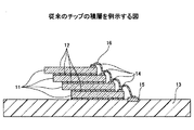
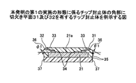
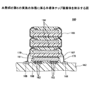
本発明の第1の実施の形態は、個片化されたチップ封止体の角部が切欠き面を有する、いわゆるベベル形状を有することを特徴とするチップ積層体の例である。
チップ封止体が積層された場合に、電気的特性向上の効果が顕著である。切欠き面の形成によって、ボンディングワイヤの端部の先端の面の面積を広くすることにより、チップ封止体を良好な条件で導電接続することができ、電気的特性を向上させることができる。また、導電性連結材33の先端の面を接続するための導電性のボンディングワイヤが、導電性連結材33の先端の面の接続箇所において接続する際に、つぶれ変形等による拡がり等を生じても、切欠き面31及び32が形成する窪みの空間内に留まる。従って、チップ封止体の側面37から導電性のボンディングワイヤの変形した部分がはみ出すことはなく、パッケージの外形寸法を所定の値に保持できる寸法的効果を有する。
図4は、本発明の第1の実施の形態の変形例に係るチップ封止体の角部に凹形の曲面41を有するチップ封止体を例示する図である。
導電性連結材とボンディングワイヤの接続箇所において、ボンディングワイヤが変形して拡がりを生じても、凹形の曲面が、平面の切欠き面の場合より大きな空間部分を形成するので、チップ封止体の側面42からボンディングワイヤの変形した部分がはみ出すことがない。従って、パッケージの外形寸法を所定の寸法に、精度よく保つことができる。
本発明の第1の実施の形態の他の変形例は、チップ封止体の上下の角部に切欠き面を設けたチップ封止体である。
係る上下の角部に切欠きを有するチップ封止体50を積層すれば、導電性連結材の露出端面を導電性のボンディングワイヤを接続するに際し、接続部分の周辺の空間を広くとることができるので、接続のためのボンディングツールの動作を円滑に行うことができる。従って、ボンディングの工程が簡素化され、また、製品品質を向上させることができる。また、切欠き面を凹形の曲面とした場合にも、同様の効果を上げることができる。
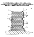
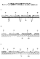
本発明の第2の実施の形態は、複数のチップ封止体と、導電性のボンディングワイヤと配線基板とを有するチップ積層体が樹脂封止された半導体チップ積層体である。
図6に示すような半導体チップ積層体60の形成によって、半導体チップを多段積層したときの積層方向の投影面積を、半導体チップのサイズに近づけることができる。また、チップ封止体の側面に沿って配線するボンディングワイヤを最短の長さにすることができるので、半導体チップ積層体の電気的特性を向上させることができる。
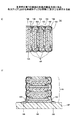
本発明の第2の実施の形態の応用例1は、2対のチップ封止体の切欠き面が対向するように積層された半導体チップ積層体である。
角部に切欠きを設けたチップ封止体を積層することにより、導電性のボンディングワイヤの接続時に、チップ封止体の接続部分の周辺の空間を広くとることができるので、ボンディングツールの動作を円滑に行うことができ、工程簡素化及び製品品質の向上を図ることができる。また、図8において、導電接続のためのボンディングワイヤ78が、導電性連結材81との接続箇所82において変形による拡がりを生じても、切欠き面71が形成する空間74a,74b,76a及び76bが、係る拡がりの部分を内包することができる。従って、導電性のボンディングワイヤの変形した部分が、チップ封止体の側面79からはみ出すことがなく、パッケージの外形寸法を所定の値に保持できる寸法的効果を有する。
本発明の第2の実施の形態の応用例2は、2対のチップ封止体の切欠き面が対向するように積層された、他の半導体チップ積層体である。
切欠き面が凹面を形成する応用例2の場合には、上記応用例1の効果を得ると共に、応用例1の平面の切欠き面の場合よりも更に広い空間を確保できるので、応用例1の効果を更に高めることができる。
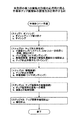
本発明の第3の実施の形態に係る発明は、半導体チップ積層体の製造方法である。
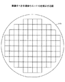
図11(a)は、準備すべき半導体ウエハ110を例示する図である。外径が6インチ、8インチ又は12インチの半導体ウエハに110にダイシングテープを貼り付け、ダイサ装置に装着後、個々の半導体チップに分離する。ウエハの厚さは、例えば50μmである。パッケージ製品の設計条件に応じて、予め所定の寸法に加工されている。
ステップ2.a)半導体チップ間隔設定において、ダイシングテープの縁辺部分をダイシングリングにより保持し半径方向の外側へ引張り拡大させ、即ちダイシングテープのエキスパンドによって、半導体チップの分離間隔を拡げる。このエキスパンドは、ダイシングリングに保持されたダイシングテープをエキスパンダ装置に装着して実施することができる。半導体チップの分離間隔は、通常100μm〜200μmとし、また、封止の条件によっては更に広く、100μmとすることができる。
チップ封止体を積層し、各チップ封止体同士の導電接続を行う。
a)チップ積層体の配線基板搭載を行い、チップ積層体と配線基板について、b)樹脂封止を行う。
ダイシングテープの引張り拡大と切欠き面の形成によって、工程の簡略化と電気的特性等の製品品質の向上を図ることができる。
本発明の第3の実施の形態の変形例は、半導体チップ積層体の他の製造方法である。半導体チップ積層体を構成するチップ封止体に関して、切欠き面を形成しない他の方法を用いることによっても、電気的特性を劣化させることなく、半導体チップ積層体を形成することができる。
導電性連結材としてのボンディングワイヤの連結された形状が、少なくとも1個の凹部を有する曲線であるときには、チップ封止体の切欠き面を設けずに、導電性連結材の露出端部の面の広い面積を確保でき、連結部の電気的特性の向上を図ることができる。また、工程の簡素化を図ることができる。
本発明の第3の実施の形態の応用例は、外部接続端子を有する複数の半導体チップ積層体の製造方法である。
a)において、複数のチップ積層体120aを共通の配線基板144の上に搭載して、b)において、配線基板144と共に絶縁樹脂145により封止し、樹脂封止した半導体チップ積層体146を形成する。
a)金属バンプ載置、b)リフローによって、金属バンプ等の外部接続端子147を接続する。金属バンプには、スズ,銀等のはんだ又は銅コアボールのはんだ等の材料を選択することができる。
配線基板の個片化すべき位置148をシャー装置等により分離切断して、パッケージ製品が得られる。
外部接続端子を有する複数のチップ積層体のパッケージを同時に製造することにより、生産性の向上を図ることができる。
本発明の第4の実施の形態は、前述の第3の実施の形態の製造方法に示した図10のステップ2.e)チップ封止体個片化から、ステップ3.a)チップ封止体積層にかけての製造工程の、他の製造方法に関するものである。一群のチップ封止体の個片化に際して使用すべきダイシングテープを置き換えて、ダイシングテープの機能を有するダイアタッチフィルムを使用することを特徴とする、半導体チップ積層体の製造方法である。
チップ封止体の個片化・積層において、従来行っていたダイアタッチフィルムの貼り付け加工とチップ封止体の個片化用のダイシングテープの貼り付け加工とを、同時に行うことができるので、工程の簡略化を図ることができる。
本発明の第5の実施の形態は、前述の第3の実施の形態の製造方法に示した図10のステップ2.e)チップ封止体個片化から、ステップ3.a)チップ封止体積層にかけての製造工程に関する、さらに他の製造方法である。一群のチップ封止体の個片化用ダイシングテープの裏面に接着層を設けることを特徴とする。
ダイアタッチフィルムに関する第4の実施の形態の効果と同様に、個片化・チップ積層において、従来行っていたダイアタッチフィルムの貼り付け加工とチップ封止体の個片化用のダイシングテープ貼り付け加工とを、同時に行うことができるので、工程の簡略化を図ることができる。
本発明の第6の実施の形態は、チップ積層体の最下層の半導体チップが、配線基板にフリップチップ実装されていることを特徴とする半導体チップ積層体である。
最下層の半導体チップが多端子を有している場合にも、配線基板と接続させて、半導体チップ積層体を形成することができる。上層に載置されるチップ積層体と組合わせることによって、本発明の半導体チップ積層体の形態を利用できる半導体チップの種類を拡大することができ、複合半導体としての機能拡張に貢献することができる。例えば、多端子のロジック回路のCPUとメモリの半導体チップの積層等を実現することができる。
本発明の第7の実施の形態は、ダイシングした半導体チップをダイアタッチフィルム(DAF)上の一定の位置に移載して行う半導体チップ積層体の製造方法である。前述の第3の実施の形態においては、半導体チップ同士の分離間隔を設定するため、ダイシングテープの引張り拡大(エキスパンド)の方法を使用したが、第7の実施の形態は、ダイシングした半導体チップを、ダイアタッチフィルム(DAF)上の一定の位置に搭載する手段を用いる。
半導体ウエハのダイシングにより個々の半導体チップを得るダイシング工程については、前出の第3の実施の形態における状態と同様であるので、説明を省く。
当ステップは、ピックアップした半導体チップが、DAF上の一定の位置に搭載され、パッド連結され、半導体チップ全体等が樹脂封止され、更に樹脂封止されたチップ封止体が個別化される工程である。図18Aの(a)から図18Cの(g)が、上記のチップ封止体の個別化までの工程を示している。
図18Aの(a)は、ダイシングテープ上の半導体ウエハが、ダイシングを終えた状態を示している。ダイシングを終えた個々の半導体チップ181は、ダイソーの切り代の間隔d1のままダイシングテープ182に置かれている。係る状態の半導体チップ181をピックアップして、新たに準備したダイアタッチフィルム上の、所定の位置に搭載する。
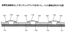
図18Bの(d)は、パッドが連結された状態を示している。パッド連結の形態は、各半導体チップを隔てている溝181aを跨ぐ形態である。係る跨ぐ形態を必要とするのは、2段階先のチップ封止体個片化(ステップ2A.のd.(図17))において、ボンディングワイヤを、ダイシングされた後の樹脂表面に露出させ、さらに導電接続するためである。樹脂表面における露出部分を広い面積として、(ステップ3A.のb.(図17))において精度よく導電接続することができる。また、パッド連結の形状は、図18Bの(d)に示すような上に凸の形状に限ることなく、ボンディングワイヤを横から見た形状が、例えば英文字のM字形をなすように制御して形成することができる。
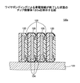
図18Bの(f)は、集積回路面、側面及び導電性連結材の樹脂封止によって、一群のチップ封止体186が形成された状態を例示する図である。半導体チップ181の裏面付近187は、既に、樹脂封止の機能を有するダイアタッチフィルム183によって封止されているので、半導体チップの未封止部分及びボンディングワイヤ(一般的には導電性連結材)を樹脂封止することによって半導体チップ及びボンディングワイヤの封止が終了する。
一群のチップ封止体186(図18Bの(f))をダイサ装置(図示せず)により個片化し、半導体チップ積層体に用いられるチップ封止体を得る。
チップ封止体の封止樹脂の表面のボンディングワイヤの露出部分に関して、その面積を広くする他の方法として、前出の(第3の実施の形態)において示したように、ダイサ装置にベベルカット用ブレードを用いて、チップ封止体の角部に切欠き面を形成することができる。すなわち、ステップ2Aのd.において、切欠き面を更に形成する方法である。その場合には、図11(f)の各部の符号を説明のために使用すると、切欠き面121における導電性連結材(ボンディングワイヤ)の端部の露出面が、導電性連結材の長手方向122に対し傾斜角度θ3を有するので、導電接続のための導電性のボンディングワイヤとの接続面を広くとることができ、良好な電気的特性を有することができる。また、(第3の実施の形態)と同様に、複数のブレードを使用するデュアルダイシング等の方法により、効率的なチップ封止体のダイシングを実施することができる。
(ステップ3A.a.チップ封止体積層)
チップ封止体を積層し、各チップ封止体同士の導電接続を行う。複数の封止チップを積層し相互に固定する。
各々のチップ封止体の表面に露出した各々の導電性連結材の端部を、導電性のボンディングワイヤにより接続する。
チップ積層体と配線基板との配線接続がパッケージ組み立ての最終工程となり、パッケージ製品が完成する。半導体チップが積層されたパッケージの製品は、配線基板を介して電子機器に搭載される。
導電接続を終了したチップ積層体191が配線基板197に載置され、ダイアタッチフィルム196により接着固定される。
図18Dの(j)において、ボンディングワイヤの端部195と配線基板197の接続端子198とが配線接続された状態を示している。以上で半導体チップ積層体の製造が終了する。
第1の効果は、製品品質、歩留まりの向上である。製造工程において、KGD(Known Good Die)についての特別な選別工程を設けることなく、KGDのみの半導体チップ積層体のパッケージを製造することができる。
配線基板と配線接続されたチップ積層体の使用条件によっては、次の図19に示すステップ4B.のような、チップ積層体に樹脂封止を施す製造方法が必要となる。
図20は、(ステップ4B.チップ積層体樹脂封止)の樹脂封止を終えたチップ積層体の状態を例示する図である。封止樹脂201によって、配線接続を終えたチップ積層体191及び配線基板197が樹脂封止された状態である。樹脂封止の方法については、トランスファーモールド法又はポッティング法等を選択する。
チップ積層体全体が樹脂封止されているので、係るチップ積層体の応用製品が、機械的、化学的に厳しい環境において使用された場合であっても、その環境に耐え得る高度の品質を提供することができる。
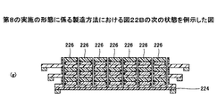
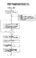
本発明の第8の実施に係る発明は、「平面を形成する一群のチップ封止体を一括積層した後に個片化する」点において、「チップ封止体を個片化後に積層する」第3〜7の実施の形態に係る製造方法の発明と異なる。固定枠に設けられたDAF(ダイアタッチフィルム)を使用し、DAF上の複数の半導体チップに対して、パッド連結及び封止を行うことによって、枠付きDAF上のチップ封止体の集合を複数形成した後、光学的位置合わせ機構等を使用して、枠ごと積層し、チップ封止体の全体が硬化した後に、ダイシングして、個々のチップ積層体を得ることを特徴とする。
第7の実施の形態その他で示したダイシングと同様であるので、本ステップの説明を省く。
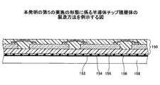
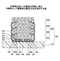
ダイアタッチフィルム(DAF)をSUS枠に貼付した状態のものを、チップ封止体の積層数の数だけ、N層分準備する。SUS枠は、製造工程にて変質、変形を生じない材料でできた固定枠であればよい。最下層に相当するSUS枠貼付のDAFに関してのみは、ダイシングテープを貼り付けた上にDAFを積層した状態で準備する。最下層のDAFは、積層したチップ封止体を個片化する時に必要となる。また、積層するための位置合わせマークを、各SUS枠に、又はDAF面に設けておく。
(ステップD. a.半導体チップピックアップ、SUS枠付きDAF上の一定位置に搭載、仮貼り付け)
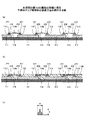
図22Aの(a)は、ダイシングされた半導体チップ221がピックアップされて、SUS枠222に貼り付けられたダイアタッチフィルム223上の一定位置に載置された配列状態を示している。半導体チップの半導体集積回路側の面の反対側の面である裏面側は、封止樹脂の機能を有するDAFによって封止された状態となる。半導体チップの配列は、例えば、3行×7列、3行×10列等、半導体チップの寸法、チップ封止体全体の寸法、チップ封止体個片化等の各条件により、決定する。
チップ封止体の導電接続に使用されるボンディングワイヤを半導体チップ上のパッドに連結する。連結方法及び連結の形態は、(第7の実施の形態)等と同様である。
図22Bの(c)は、集積回路面、側面及び導電性連結材(ボンディングワイヤ)の樹脂封止後の状態を示している。パッド連結及び集積回路面樹脂封止に関しては、(第7の実施の形態)のステップ2A.の説明と重複するので、説明を省く。
積層の数が増加する場合にも、係る関係と同様の関係を保つことによって、積層を円滑に行うことができる。
各層を構成するチップ封止体が、SUS枠上のダイアタッチフィルムに搭載されたまま一括積層される工程である。
チップ封止体の内部にある半導体チップが、縦横に配列されたままで積層された状態、すなわち、半導体チップがマトリックス状になったチップ封止体の集合体を、ダイサ装置を用いて、一括して個片化する工程である。チップ封止体個片化のダイシングに際しては、寸法精度を確保するため、光学的機構及び位置制御システムを使用する。
ダイシングテープ(図22Cの(g)の224)上の個片化された各チップ封止体226をピックアップして、導電接続を行う。係る導電接続及び次の(ステップH.チップ積層体の配線接続)に関しては、(第7の実施の形態)その他で示した工程の内容と同様であるので、説明を省く。以上の工程によって、前出の図18Dの(j)に示されたような、配線接続が終了したチップ積層体を得ることができる。
第8の実施の形態においては、個片化の工程について、チップ封止体の積層後に一括して個片化を行うことにより、(第7の実施の形態)に対して、チップ封止体個片化のダイシングの回数が大幅に減少し、工程の簡略化と製品品質の向上を図ることができる。
本発明の第8の実施の形態の変形例は、2層の樹脂層を有するダイアタッチフィルムを用いることにより一括して封止積層する製造方法である。物性の異なる2層の樹脂層を有するダイアタッチフィルムを用いて、パッド連結のボンディングワイヤ側等の封止と半導体チップの裏面付近、すなわち、半導体集積回路側の面の反対側の面付近の封止とを、一括積層時に同時に行う製造方法である。パッド連結に使用されているボンディングワイヤ部分等を封止する樹脂には、低粘度を維持する封止樹脂を要するため、所定の低粘度の物性を有する樹脂層を積層した2層のダイアタッチフィルムを準備する。
前出の第7の実施の形態その他で示したダイシングと同様であるので、説明を省く。
積層の層数分のSUS枠に貼り付けたダイアタッチフィルムを準備する。
最上層に位置するチップ封止体層に相当する部分の半導体集積回路側及びパッド連結のボンディングワイヤ側等を封止するため、「樹脂フィルム2」のみをSUS枠に貼り付けたものを準備する。この「樹脂フィルム2」とは、低粘度性の物性を有する封止樹脂のフィルムを指し、その使用の理由は、以下の通りである。
半導体チップの裏面付近を封止するダイアタッチフィルム本体を「樹脂フィルム1」とし、係る「樹脂フィルム1」と「樹脂フィルム2」の2種のフィルムを積層したフィルムを、第2層以下のチップ封止体に対し、ダイアタッチフィルムとして準備する。
チップ積層体の個片化のため、ダイシングテープを準備し、その上に「樹脂フィルム1」を貼り付けた状態のSUS枠付きダイアタッチフィルムを準備する。
ボンディングワイヤを用いたパッド連結は、(第8の実施の形態)等と同様である。
SUS枠の使用によって、多数の半導体チップの樹脂封止及び積層を一括して行うステップである。
(ステップF.チップ封止体個片化)
(ステップG.導電接続)
(ステップH.チップ積層体の配線接続)
の工程は、第8の実施の形態における工程と同様であるので、重複を避け、説明を省く。以上によって、第8の実施の形態の変形例である「2層を有するダイアタッチフィルムを用いた一括封止積層」を行うチップ積層体の製造方法が終了する。
また、配線接続を終了したチップ積層体の樹脂封止も可能である。(第7の実施の形態の応用例)において図20に示したように、配線接続を終了したチップ積層体及び配線基板を樹脂封止してもよい。
2層を有するダイアタッチフィルムを用いることによって、半導体チップの裏面付近以外の封止、すなわちパッドを連結しているボンディングワイヤ部分及び半導体チップの半導体集積回路面と側面等を封止するための個別の封止の工程を設けることなく、全体の一括封止積層の工程において同時に一回で封止及び積層を実施することができるので、工程の簡略化を図ることができる。
図25は、本発明の第9の実施の形態に係る、チップ積層体250の最下層の半導体チップ251の、配線基板197へのフリップチップ実装を特徴とする半導体チップ積層体260を例示する図である。図25の(a)及び(b)は、樹脂封止材263の形状のみが相違している。
ほぼチップサイズの小型化されたチップ積層体を、配線基板上にフリップチップ実装することができるので、半導体チップ積層体の性能、品質の向上を図ることができる。
図26は、本発明の第10の実施の形態に係る半導体チップ積層体の製造方法のステップを例示する図である。本製造方法は、チップ積層体の有する最下層のチップ封止体が、配線基板にフリップチップ接続されていることを特徴とする。前述の第3の実施の形態に係る製造方法のステップ(図10)と対比すると、(ステップ2B.チップ封止体形成)におけるb2.バンプ形成及び(ステップ4A.チップ積層体樹脂封止)におけるa1.チップ積層体の配線基板搭載(フリップチップ接続)基板加熱、フリップチップ接続の工程が相違している。そこで、相違する2つの工程を中心に、次の図27及び図28を参照して説明し、(ステップ2B.チップ封止体形成)における他の工程及び(ステップ3.導電接続)の工程等については、記載の重複を避けるため、その説明を省く。
図27は、チップ封止体形成ステップにおけるフリップチップ接続のためのバンプが形成された状態を例示する図である。図27の(a)は、その全体図を、(b)は絶縁樹脂による封止後の状態を、(c)は、1個のバンプを示している。なお、前述の図11(c1)における対応する箇所の同一の符号を使用した。
図28は、チップ積層体280がフリップチップ実装によって配線基板に搭載されている状態を例示する図である。
チップ積層体を、配線基板にフリップチップ実装する製造方法を提供することにより、短時間で、ほぼチップサイズの小型化されたチップ積層体の配線基板への実装が実現でき、半導体チップ積層体の生産性の向上及び品質の向上を図ることができる。
図29は、本発明の第11の実施の形態に係る、他のチップ積層体290がフリップチップ実装によって配線基板197に搭載されている状態を例示する図である。最下層の半導体チップ291が、能動素子側の表面のパッド292上に設けられたバンプ293とボンディングワイヤ256上のバンプ261とを介して配線基板197にフリップチップ接続されている。
本発明の半導体チップ積層体の形態を利用できる半導体チップの種類を拡大することができ、複合半導体としての機能拡張に貢献することができる。例えば、多端子のロジック回路のCPUとメモリの半導体チップの積層等を実現することができる。
以上、本発明の好ましい実施の形態について詳説したが、本発明は、上述した実施の形態に制限されることはなく、本発明の範囲を逸脱することなく、上述した実施の形態に種々の変形及び置換を加えることができる。
11,21,111,181,221 半導体チップ
13,65,75,131,144,197 配線基板
14,22,113,255 パッド
15,67,135,169,198,262B 接続端子
16,64,78,133,165,192,258 ボンディングワイヤ
21a,115 半導体チップの集積回路面
21b,116 半導体チップの側面
21c,117 半導体チップの裏面
23,33,81 導電性連結材
24 導電性連結材の外部装置側の端部の先端の面
25,50,61,71a,71b,72a,72b,73,120,164,188,259 チップ封止体
26,27,68,116b,117b,145,252,253 絶縁樹脂
28 チップ封止体の角部
31,32,51,52,71,72,121 切欠き面
41 凹形の曲面
37,42 チップ封止体の側面
60,70,140,160,260 半導体チップ積層体
62 角部の切欠き面
63 角部の切欠き面に露出した導電性連結材の端部
66,132,152,156 接着層
74a,76a チップ封止体71aの切欠き面71が形成する空間
74b,76b チップ封止体71bの切欠き面71が形成する空間
77 チップ封止体71aとチップ封止体71bの重ね合わせ面
79 チップ封止体の導電性のボンディングワイヤの側面
82 ボンディングワイヤ78の導電性連結材81との接続箇所
94a,96a チップ封止体91aの切欠き面91が形成する空間
94b,96b チップ封止体91bの切欠き面91が形成する空間
97 チップ封止体91aとチップ封止体91bの重ね合わせ面
110 半導体ウエハ
112 ダイシングテープ
114,141,185,193,256 ボンディングワイヤ(導電性連結材)
118,150 一群のチップ封止体
119,154 チップ封止体の個片化用のダイシングテープ
120a,189,191,250,280,290 チップ積層体
122 導電性連結材の長手方向
123 チップ積層用架台
124,151,167 ダイアタッチフィルム
125 凹部
134 ボンディングワイヤ133の端部
142 ボンディングワイヤ141の端部の先端の面
147 外部接続端子
157,158,183A テープ基材
161,251 最下層の半導体チップ
163 接続バンプ
166 アンダーフィル
170 ボンディングワイヤ165の端部
180 ステップ2Aのc.において封止に使用される樹脂
181a 各半導体チップを隔てている溝
182 ダイシングテープ
183,196,223 ダイアタッチフィルム
184 半導体チップ181の下方側面
186 一群のチップ封止体
187 半導体チップ181の裏面付近
194 ボンディングワイヤ(導電性連結材)193の端面
195 ボンディングワイヤ192の端部
201 封止樹脂
222,225a,225b,225c,243a,243b,243c,243d SUS枠
224 ダイシングテープ
226 個片化された各チップ封止体
241 樹脂フィルム1
242 樹脂フィルム2
254 最下層のチップ封止体
257 ボンディングワイヤ256の端面
261,270 バンプ
262A はんだ端子
271 尖頭部
d バンプの直径
d1 ブレードによる切り代
d2,d3 樹脂の厚さ
h バンプの高さ
θ1,θ2,φ1,φ2 切欠き面が集積回路面に対してなす角度
θ3 切欠き面121における導電性連結材の端部の露出面が、導電性連結材の長手方向122に対しなす傾斜角度
θ4 ボンディングワイヤ141の端部の先端の面142が、ボンディングワイヤの長手方向X−Xとなす傾斜角度
W1o,W2o,W3o,U1o,U2o,U3o,U4o SUS枠の外側の幅の寸法
W1i,W2i,W3i,U1i,U2i,U3i,U4i SUS枠の内側の幅の寸法
Claims (16)
- 接続端子を有する配線基板と、
前記配線基板上に積層された複数のチップ封止体と、を有し、
それぞれの前記チップ封止体は、半導体集積回路、パッド、及び前記パッドと外部装置とを接続する第1ボンディングワイヤを備えた半導体チップと、前記第1ボンディングワイヤの前記外部装置側の端部を露出するように前記半導体チップの全面を封止する樹脂と、を含み、
前記樹脂は、前記半導体チップの集積回路面及び側面並びに前記第1ボンディングワイヤを封止する第1樹脂と、前記半導体チップの集積回路面と反対側の面を封止する第2樹脂と、を含み、
前記接続端子と、それぞれの前記チップ封止体の前記第1ボンディングワイヤの前記外部装置側の端部とは、第2ボンディングワイヤを介して導電接続され、
前記複数のチップ封止体、前記第2ボンディングワイヤ、及び前記接続端子は、樹脂封止材に封止されている半導体チップ積層体。 - 前記第1樹脂は、
平面又は凹形の曲面の切欠き面を有する角部を有し、
前記第1ボンディングワイヤの前記外部装置側の端部は、前記第1ボンディングワイヤの長手方向に対して傾斜を有するように切断されて前記切欠き面から露出している請求項1記載の半導体チップ積層体。 - 一対の、又は複数対の前記チップ封止体の切欠き面が対向するように積層され、それぞれの前記切欠き面が形成する空間の形状が、前記一対の、又は複数対の前記チップ封止体の各重ね合わせ面を対称面とする、面対称な形状である請求項2記載の半導体チップ積層体。
- 前記チップ封止体の第2樹脂が、ダイアタッチフィルムである請求項1乃至3の何れか一項記載の半導体チップ積層体。
- 前記第2ボンディングワイヤは、前記チップ封止体の側面に接触して形成されている請求項1乃至4の何れか一項記載の半導体チップ積層体。
- それぞれの前記チップ封止体の前記第1ボンディングワイヤの前記外部装置側の端部と前記第2ボンディングワイヤとは直接接続されている請求項1乃至5の何れか一項記載の半導体チップ積層体。
- 半導体集積回路及びパッドを備えた半導体チップとなる複数の領域を有する半導体ウエハにダイシングテープを貼り付け、前記半導体ウエハをダイシングし、前記ダイシングテープ上に所定間隔で配置された複数の半導体チップを作製するダイシング工程と、
前記ダイシング工程により得られた個々の前記半導体チップのうち、隣接する前記半導体チップの前記パッド間を第1ボンディングワイヤにより導電接続するパッド接続工程と、
前記ダイシングテープ上に、前記半導体チップ及び前記第1ボンディングワイヤを封止する第1樹脂を形成する第1樹脂形成工程と、
前記ダイシングテープを剥離する剥離工程と、
前記半導体チップ及び前記第1樹脂の前記剥離工程で露出した部分を封止する第2樹脂を形成する第2樹脂形成工程と、
隣接する前記半導体チップ間に位置する前記第1樹脂、前記第1ボンディングワイヤ、及び前記第2樹脂を切断して、前記第1ボンディングワイヤの端部が前記第1樹脂から露出する複数のチップ封止体を形成するチップ封止体形成工程と、
前記複数のチップ封止体を積層し、各々の前記チップ封止体の前記第1樹脂から露出する前記第1ボンディングワイヤの端部同士を第2ボンディングワイヤにより相互に接続してチップ積層体を形成するチップ積層体形成工程と、
前記チップ積層体を配線基板上に搭載し、前記チップ積層体と前記配線基板とを封止する第3樹脂を形成する第3樹脂形成工程と、を有する半導体チップ積層体の製造方法。 - 前記ダイシング工程と前記パッド接続工程との間に、ダイシングテープの引張り拡大工程を有する請求項7記載の半導体チップ積層体の製造方法。
- 前記チップ封止体の角部を切欠いて形成される切欠き面内に、前記第1ボンディングワイヤの端部を露出させる角部切欠き工程を有する請求項7又は8記載の半導体チップ積層体の製造方法。
- 前記パッド接続工程では、隣接する前記半導体チップの前記パッド間の前記第1ボンディングワイヤを含む面内における前記第1ボンディングワイヤの形状が、少なくとも1個の凹部を有する曲線となるように形成される請求項7乃至9の何れか一項記載の半導体チップ積層体の製造方法。
- 前記第2樹脂として、ダイシングテープの機能を有するダイアタッチフィルムを使用する請求項7乃至10の何れか一項記載の半導体チップ積層体の製造方法。
- 前記第2樹脂形成工程と前記チップ封止体形成工程との間に、前記第2樹脂の前記半導体チップを封止する面とは反対側の面に前記チップ封止体の個片化用のダイシングテープを貼り付ける工程を有し、
前記個片化用のダイシングテープが、前記チップ封止体との接着面の反対側の面に接着層を有する請求項7乃至10の何れか一項記載の半導体チップ積層体の製造方法。 - 半導体集積回路及びパッドを備えた半導体チップとなる複数の領域を有する半導体ウエハをダイシングし、複数の半導体チップを形成するダイシング工程と、
前記ダイシング工程により得られた個々の前記半導体チップを、ダイアタッチフィルム上に所定間隔で搭載する半導体チップ搭載工程と、
前記ダイアタッチフィルム上に搭載された個々の前記半導体チップのうち、隣接する前記半導体チップの前記パッド間を第1ボンディングワイヤにより導電接続するパッド接続工程と、
前記ダイアタッチフィルム上に、前記半導体チップ及び前記第1ボンディングワイヤを封止する樹脂を形成する樹脂形成工程と、
隣接する前記半導体チップ間に位置する前記樹脂、前記第1ボンディングワイヤ、及び前記ダイアタッチフィルムを切断して、前記第1ボンディングワイヤの端部が前記樹脂から露出する複数のチップ封止体を形成するチップ封止体形成工程と、
前記複数のチップ封止体を積層し、各々の前記チップ封止体の前記樹脂から露出する前記第1ボンディングワイヤの端部同士を第2ボンディングワイヤにより相互に接続してチップ積層体を形成するチップ積層体形成工程と、
前記チップ積層体を配線基板上に搭載し、前記チップ積層体と前記配線基板とを配線接続する配線接続工程と、を有する半導体チップ積層体の製造方法。 - 前記配線接続された前記チップ積層体と前記配線基板を樹脂封止するチップ積層体樹脂封止工程を有する請求項13記載の半導体チップ積層体の製造方法。
- 前記チップ封止体の角部を切欠いて形成される切欠き面内に、前記第1ボンディングワイヤの端部を露出させる角部切欠き工程を有する請求項13又は14記載の半導体チップ積層体の製造方法。
- 前記パッド接続工程では、隣接する前記半導体チップの前記パッド間の前記第1ボンディングワイヤを含む面内における前記第1ボンディングワイヤの形状が、少なくとも1個の凹部を有する曲線となるように形成される請求項13乃至15の何れか一項記載の半導体チップ積層体の製造方法。
Priority Applications (2)
| Application Number | Priority Date | Filing Date | Title |
|---|---|---|---|
| JP2009266485A JP5700927B2 (ja) | 2008-11-28 | 2009-11-24 | 半導体装置及び半導体装置の製造方法 |
| US12/626,069 US8394678B2 (en) | 2008-11-28 | 2009-11-25 | Semiconductor chip stacked body and method of manufacturing the same |
Applications Claiming Priority (7)
| Application Number | Priority Date | Filing Date | Title |
|---|---|---|---|
| JP2008305187 | 2008-11-28 | ||
| JP2008305187 | 2008-11-28 | ||
| JP2009010828 | 2009-01-21 | ||
| JP2009010828 | 2009-01-21 | ||
| JP2009149116 | 2009-06-23 | ||
| JP2009149116 | 2009-06-23 | ||
| JP2009266485A JP5700927B2 (ja) | 2008-11-28 | 2009-11-24 | 半導体装置及び半導体装置の製造方法 |
Publications (3)
| Publication Number | Publication Date |
|---|---|
| JP2011029581A JP2011029581A (ja) | 2011-02-10 |
| JP2011029581A5 JP2011029581A5 (ja) | 2012-12-06 |
| JP5700927B2 true JP5700927B2 (ja) | 2015-04-15 |
Family
ID=42222015
Family Applications (1)
| Application Number | Title | Priority Date | Filing Date |
|---|---|---|---|
| JP2009266485A Expired - Fee Related JP5700927B2 (ja) | 2008-11-28 | 2009-11-24 | 半導体装置及び半導体装置の製造方法 |
Country Status (2)
| Country | Link |
|---|---|
| US (1) | US8394678B2 (ja) |
| JP (1) | JP5700927B2 (ja) |
Families Citing this family (9)
| Publication number | Priority date | Publication date | Assignee | Title |
|---|---|---|---|---|
| JP4776675B2 (ja) * | 2008-10-31 | 2011-09-21 | 株式会社東芝 | 半導体メモリカード |
| MY152355A (en) | 2011-04-11 | 2014-09-15 | Carsem M Sdn Bhd | Short and low loop wire bonding |
| US9704797B2 (en) * | 2011-05-18 | 2017-07-11 | Sandisk Information Technology (Shanghai) Co., Ltd. | Waterfall wire bonding |
| KR20120135626A (ko) * | 2011-06-07 | 2012-12-17 | 삼성전자주식회사 | 반도체 칩 패키지의 제조 방법 |
| MY181180A (en) | 2011-09-09 | 2020-12-21 | Carsem M Sdn Bhd | Low loop wire bonding |
| US9595487B2 (en) * | 2013-06-25 | 2017-03-14 | Infineon Technologies Ag | Circuit arrangement and method for manufacturing the same |
| CN106686932B (zh) * | 2015-11-05 | 2019-12-13 | 精能医学股份有限公司 | 植入式电子装置的防水结构 |
| US10923456B2 (en) * | 2018-12-20 | 2021-02-16 | Cerebras Systems Inc. | Systems and methods for hierarchical exposure of an integrated circuit having multiple interconnected die |
| JP2022047990A (ja) | 2020-09-14 | 2022-03-25 | キオクシア株式会社 | 半導体装置の製造方法、及び半導体製造装置 |
Family Cites Families (13)
| Publication number | Priority date | Publication date | Assignee | Title |
|---|---|---|---|---|
| US5675180A (en) | 1994-06-23 | 1997-10-07 | Cubic Memory, Inc. | Vertical interconnect process for silicon segments |
| JP3847432B2 (ja) * | 1997-12-25 | 2006-11-22 | 沖電気工業株式会社 | 樹脂封止半導体装置及びその製造方法 |
| US6207474B1 (en) * | 1998-03-09 | 2001-03-27 | Micron Technology, Inc. | Method of forming a stack of packaged memory die and resulting apparatus |
| US6291894B1 (en) * | 1998-08-31 | 2001-09-18 | Micron Technology, Inc. | Method and apparatus for a semiconductor package for vertical surface mounting |
| JP3476383B2 (ja) * | 1999-05-27 | 2003-12-10 | シャープ株式会社 | 半導体積層パッケージ |
| JP2001156250A (ja) * | 1999-11-24 | 2001-06-08 | Seiko Epson Corp | 半導体チップ、マルチチップパッケージ,および半導体装置と、並びに、それを用いた電子機器 |
| JP4361670B2 (ja) * | 2000-08-02 | 2009-11-11 | 富士通マイクロエレクトロニクス株式会社 | 半導体素子積層体、半導体素子積層体の製造方法、及び半導体装置 |
| JP2005191342A (ja) * | 2003-12-26 | 2005-07-14 | Renesas Technology Corp | 半導体装置およびその製造方法 |
| JP4398305B2 (ja) * | 2004-06-02 | 2010-01-13 | カシオ計算機株式会社 | 半導体装置およびその製造方法 |
| US20070158807A1 (en) * | 2005-12-29 | 2007-07-12 | Daoqiang Lu | Edge interconnects for die stacking |
| US8723332B2 (en) * | 2007-06-11 | 2014-05-13 | Invensas Corporation | Electrically interconnected stacked die assemblies |
| US7892894B2 (en) * | 2007-09-20 | 2011-02-22 | Stats Chippac Ltd. | Method of manufacturing integrated circuit package system with warp-free chip |
| US7843046B2 (en) * | 2008-02-19 | 2010-11-30 | Vertical Circuits, Inc. | Flat leadless packages and stacked leadless package assemblies |
-
2009
- 2009-11-24 JP JP2009266485A patent/JP5700927B2/ja not_active Expired - Fee Related
- 2009-11-25 US US12/626,069 patent/US8394678B2/en not_active Expired - Fee Related
Also Published As
| Publication number | Publication date |
|---|---|
| US20100133677A1 (en) | 2010-06-03 |
| JP2011029581A (ja) | 2011-02-10 |
| US8394678B2 (en) | 2013-03-12 |
Similar Documents
| Publication | Publication Date | Title |
|---|---|---|
| JP5700927B2 (ja) | 半導体装置及び半導体装置の製造方法 | |
| US8076770B2 (en) | Semiconductor device including a first land on the wiring substrate and a second land on the sealing portion | |
| US8786102B2 (en) | Semiconductor device and method of manufacturing the same | |
| US9165870B2 (en) | Semiconductor storage device and manufacturing method thereof | |
| US9397072B2 (en) | Method of manufacturing semiconductor device | |
| US9099459B2 (en) | Semiconductor device and manufacturing method of the same | |
| US9583455B2 (en) | Semiconductor device | |
| US8058717B2 (en) | Laminated body of semiconductor chips including pads mutually connected to conductive member | |
| US20110062596A1 (en) | Semiconductor chip stacked structure and method of manufacturing same | |
| US20090127682A1 (en) | Chip package structure and method of fabricating the same | |
| CN110718544B (zh) | 半导体装置 | |
| US20210082895A1 (en) | Semiconductor device and manufacturing method thereof | |
| US8101461B2 (en) | Stacked semiconductor device and method of manufacturing the same | |
| JP2009105334A (ja) | 半導体装置及びその製造方法 | |
| JP2009212315A (ja) | 半導体装置及びその製造方法 | |
| KR20060101385A (ko) | 반도체 장치 및 그 제조 방법 | |
| JP2015177061A (ja) | 半導体装置の製造方法および半導体装置 | |
| JP5921297B2 (ja) | 積層型半導体装置、プリント回路板及び積層型半導体装置の製造方法 | |
| US8217517B2 (en) | Semiconductor device provided with wire that electrically connects printed wiring board and semiconductor chip each other | |
| JP2014167973A (ja) | 半導体装置およびその製造方法 | |
| CN110634880A (zh) | 半导体装置及其制造方法 | |
| JP2011023709A (ja) | 半導体装置及びその製造方法 | |
| JP5234703B2 (ja) | 半導体装置の製造方法 | |
| US20220384468A1 (en) | Semiconductor device and semiconductor device manufacturing method | |
| JP2011210936A (ja) | 半導体装置の製造方法および半導体装置 |
Legal Events
| Date | Code | Title | Description |
|---|---|---|---|
| A521 | Request for written amendment filed |
Free format text: JAPANESE INTERMEDIATE CODE: A523 Effective date: 20121019 |
|
| A621 | Written request for application examination |
Free format text: JAPANESE INTERMEDIATE CODE: A621 Effective date: 20121019 |
|
| A131 | Notification of reasons for refusal |
Free format text: JAPANESE INTERMEDIATE CODE: A131 Effective date: 20140304 |
|
| A521 | Request for written amendment filed |
Free format text: JAPANESE INTERMEDIATE CODE: A523 Effective date: 20140414 |
|
| A131 | Notification of reasons for refusal |
Free format text: JAPANESE INTERMEDIATE CODE: A131 Effective date: 20140909 |
|
| A521 | Request for written amendment filed |
Free format text: JAPANESE INTERMEDIATE CODE: A523 Effective date: 20140917 |
|
| TRDD | Decision of grant or rejection written | ||
| A01 | Written decision to grant a patent or to grant a registration (utility model) |
Free format text: JAPANESE INTERMEDIATE CODE: A01 Effective date: 20150210 |
|
| A61 | First payment of annual fees (during grant procedure) |
Free format text: JAPANESE INTERMEDIATE CODE: A61 Effective date: 20150217 |
|
| R150 | Certificate of patent or registration of utility model |
Ref document number: 5700927 Country of ref document: JP Free format text: JAPANESE INTERMEDIATE CODE: R150 |
|
| LAPS | Cancellation because of no payment of annual fees |