JP5700927B2 - Semiconductor device and manufacturing method of semiconductor device - Google Patents
Semiconductor device and manufacturing method of semiconductor device Download PDFInfo
- Publication number
- JP5700927B2 JP5700927B2 JP2009266485A JP2009266485A JP5700927B2 JP 5700927 B2 JP5700927 B2 JP 5700927B2 JP 2009266485 A JP2009266485 A JP 2009266485A JP 2009266485 A JP2009266485 A JP 2009266485A JP 5700927 B2 JP5700927 B2 JP 5700927B2
- Authority
- JP
- Japan
- Prior art keywords
- chip
- resin
- bonding wire
- sealing
- semiconductor chip
- Prior art date
- Legal status (The legal status is an assumption and is not a legal conclusion. Google has not performed a legal analysis and makes no representation as to the accuracy of the status listed.)
- Expired - Fee Related
Links
Images


Classifications
-
- H—ELECTRICITY
- H01—ELECTRIC ELEMENTS
- H01L—SEMICONDUCTOR DEVICES NOT COVERED BY CLASS H10
- H01L23/00—Details of semiconductor or other solid state devices
- H01L23/48—Arrangements for conducting electric current to or from the solid state body in operation, e.g. leads, terminal arrangements ; Selection of materials therefor
- H01L23/488—Arrangements for conducting electric current to or from the solid state body in operation, e.g. leads, terminal arrangements ; Selection of materials therefor consisting of soldered or bonded constructions
- H01L23/495—Lead-frames or other flat leads
- H01L23/49572—Lead-frames or other flat leads consisting of thin flexible metallic tape with or without a film carrier
-
- H—ELECTRICITY
- H01—ELECTRIC ELEMENTS
- H01L—SEMICONDUCTOR DEVICES NOT COVERED BY CLASS H10
- H01L21/00—Processes or apparatus adapted for the manufacture or treatment of semiconductor or solid state devices or of parts thereof
- H01L21/02—Manufacture or treatment of semiconductor devices or of parts thereof
- H01L21/04—Manufacture or treatment of semiconductor devices or of parts thereof the devices having at least one potential-jump barrier or surface barrier, e.g. PN junction, depletion layer or carrier concentration layer
- H01L21/50—Assembly of semiconductor devices using processes or apparatus not provided for in a single one of the subgroups H01L21/06 - H01L21/326, e.g. sealing of a cap to a base of a container
- H01L21/56—Encapsulations, e.g. encapsulation layers, coatings
- H01L21/568—Temporary substrate used as encapsulation process aid
-
- H—ELECTRICITY
- H01—ELECTRIC ELEMENTS
- H01L—SEMICONDUCTOR DEVICES NOT COVERED BY CLASS H10
- H01L23/00—Details of semiconductor or other solid state devices
- H01L23/28—Encapsulations, e.g. encapsulating layers, coatings, e.g. for protection
- H01L23/31—Encapsulations, e.g. encapsulating layers, coatings, e.g. for protection characterised by the arrangement or shape
- H01L23/3107—Encapsulations, e.g. encapsulating layers, coatings, e.g. for protection characterised by the arrangement or shape the device being completely enclosed
- H01L23/3121—Encapsulations, e.g. encapsulating layers, coatings, e.g. for protection characterised by the arrangement or shape the device being completely enclosed a substrate forming part of the encapsulation
-
- H—ELECTRICITY
- H01—ELECTRIC ELEMENTS
- H01L—SEMICONDUCTOR DEVICES NOT COVERED BY CLASS H10
- H01L23/00—Details of semiconductor or other solid state devices
- H01L23/48—Arrangements for conducting electric current to or from the solid state body in operation, e.g. leads, terminal arrangements ; Selection of materials therefor
- H01L23/488—Arrangements for conducting electric current to or from the solid state body in operation, e.g. leads, terminal arrangements ; Selection of materials therefor consisting of soldered or bonded constructions
- H01L23/495—Lead-frames or other flat leads
- H01L23/49541—Geometry of the lead-frame
- H01L23/49548—Cross section geometry
- H01L23/49551—Cross section geometry characterised by bent parts
- H01L23/49555—Cross section geometry characterised by bent parts the bent parts being the outer leads
-
- H—ELECTRICITY
- H01—ELECTRIC ELEMENTS
- H01L—SEMICONDUCTOR DEVICES NOT COVERED BY CLASS H10
- H01L24/00—Arrangements for connecting or disconnecting semiconductor or solid-state bodies; Methods or apparatus related thereto
- H01L24/01—Means for bonding being attached to, or being formed on, the surface to be connected, e.g. chip-to-package, die-attach, "first-level" interconnects; Manufacturing methods related thereto
- H01L24/18—High density interconnect [HDI] connectors; Manufacturing methods related thereto
- H01L24/23—Structure, shape, material or disposition of the high density interconnect connectors after the connecting process
- H01L24/24—Structure, shape, material or disposition of the high density interconnect connectors after the connecting process of an individual high density interconnect connector
-
- H—ELECTRICITY
- H01—ELECTRIC ELEMENTS
- H01L—SEMICONDUCTOR DEVICES NOT COVERED BY CLASS H10
- H01L24/00—Arrangements for connecting or disconnecting semiconductor or solid-state bodies; Methods or apparatus related thereto
- H01L24/01—Means for bonding being attached to, or being formed on, the surface to be connected, e.g. chip-to-package, die-attach, "first-level" interconnects; Manufacturing methods related thereto
- H01L24/42—Wire connectors; Manufacturing methods related thereto
- H01L24/47—Structure, shape, material or disposition of the wire connectors after the connecting process
- H01L24/48—Structure, shape, material or disposition of the wire connectors after the connecting process of an individual wire connector
-
- H—ELECTRICITY
- H01—ELECTRIC ELEMENTS
- H01L—SEMICONDUCTOR DEVICES NOT COVERED BY CLASS H10
- H01L24/00—Arrangements for connecting or disconnecting semiconductor or solid-state bodies; Methods or apparatus related thereto
- H01L24/80—Methods for connecting semiconductor or other solid state bodies using means for bonding being attached to, or being formed on, the surface to be connected
- H01L24/82—Methods for connecting semiconductor or other solid state bodies using means for bonding being attached to, or being formed on, the surface to be connected by forming build-up interconnects at chip-level, e.g. for high density interconnects [HDI]
-
- H—ELECTRICITY
- H01—ELECTRIC ELEMENTS
- H01L—SEMICONDUCTOR DEVICES NOT COVERED BY CLASS H10
- H01L24/00—Arrangements for connecting or disconnecting semiconductor or solid-state bodies; Methods or apparatus related thereto
- H01L24/91—Methods for connecting semiconductor or solid state bodies including different methods provided for in two or more of groups H01L24/80 - H01L24/90
-
- H—ELECTRICITY
- H01—ELECTRIC ELEMENTS
- H01L—SEMICONDUCTOR DEVICES NOT COVERED BY CLASS H10
- H01L24/00—Arrangements for connecting or disconnecting semiconductor or solid-state bodies; Methods or apparatus related thereto
- H01L24/93—Batch processes
- H01L24/95—Batch processes at chip-level, i.e. with connecting carried out on a plurality of singulated devices, i.e. on diced chips
- H01L24/97—Batch processes at chip-level, i.e. with connecting carried out on a plurality of singulated devices, i.e. on diced chips the devices being connected to a common substrate, e.g. interposer, said common substrate being separable into individual assemblies after connecting
-
- H—ELECTRICITY
- H01—ELECTRIC ELEMENTS
- H01L—SEMICONDUCTOR DEVICES NOT COVERED BY CLASS H10
- H01L25/00—Assemblies consisting of a plurality of individual semiconductor or other solid state devices ; Multistep manufacturing processes thereof
- H01L25/03—Assemblies consisting of a plurality of individual semiconductor or other solid state devices ; Multistep manufacturing processes thereof all the devices being of a type provided for in the same subgroup of groups H01L27/00 - H01L33/00, or in a single subclass of H10K, H10N, e.g. assemblies of rectifier diodes
- H01L25/04—Assemblies consisting of a plurality of individual semiconductor or other solid state devices ; Multistep manufacturing processes thereof all the devices being of a type provided for in the same subgroup of groups H01L27/00 - H01L33/00, or in a single subclass of H10K, H10N, e.g. assemblies of rectifier diodes the devices not having separate containers
- H01L25/065—Assemblies consisting of a plurality of individual semiconductor or other solid state devices ; Multistep manufacturing processes thereof all the devices being of a type provided for in the same subgroup of groups H01L27/00 - H01L33/00, or in a single subclass of H10K, H10N, e.g. assemblies of rectifier diodes the devices not having separate containers the devices being of a type provided for in group H01L27/00
- H01L25/0657—Stacked arrangements of devices
-
- H—ELECTRICITY
- H01—ELECTRIC ELEMENTS
- H01L—SEMICONDUCTOR DEVICES NOT COVERED BY CLASS H10
- H01L25/00—Assemblies consisting of a plurality of individual semiconductor or other solid state devices ; Multistep manufacturing processes thereof
- H01L25/50—Multistep manufacturing processes of assemblies consisting of devices, each device being of a type provided for in group H01L27/00 or H01L29/00
-
- H—ELECTRICITY
- H01—ELECTRIC ELEMENTS
- H01L—SEMICONDUCTOR DEVICES NOT COVERED BY CLASS H10
- H01L2224/00—Indexing scheme for arrangements for connecting or disconnecting semiconductor or solid-state bodies and methods related thereto as covered by H01L24/00
- H01L2224/01—Means for bonding being attached to, or being formed on, the surface to be connected, e.g. chip-to-package, die-attach, "first-level" interconnects; Manufacturing methods related thereto
- H01L2224/02—Bonding areas; Manufacturing methods related thereto
- H01L2224/023—Redistribution layers [RDL] for bonding areas
- H01L2224/0233—Structure of the redistribution layers
-
- H—ELECTRICITY
- H01—ELECTRIC ELEMENTS
- H01L—SEMICONDUCTOR DEVICES NOT COVERED BY CLASS H10
- H01L2224/00—Indexing scheme for arrangements for connecting or disconnecting semiconductor or solid-state bodies and methods related thereto as covered by H01L24/00
- H01L2224/01—Means for bonding being attached to, or being formed on, the surface to be connected, e.g. chip-to-package, die-attach, "first-level" interconnects; Manufacturing methods related thereto
- H01L2224/02—Bonding areas; Manufacturing methods related thereto
- H01L2224/023—Redistribution layers [RDL] for bonding areas
- H01L2224/0237—Disposition of the redistribution layers
- H01L2224/02371—Disposition of the redistribution layers connecting the bonding area on a surface of the semiconductor or solid-state body with another surface of the semiconductor or solid-state body
-
- H—ELECTRICITY
- H01—ELECTRIC ELEMENTS
- H01L—SEMICONDUCTOR DEVICES NOT COVERED BY CLASS H10
- H01L2224/00—Indexing scheme for arrangements for connecting or disconnecting semiconductor or solid-state bodies and methods related thereto as covered by H01L24/00
- H01L2224/01—Means for bonding being attached to, or being formed on, the surface to be connected, e.g. chip-to-package, die-attach, "first-level" interconnects; Manufacturing methods related thereto
- H01L2224/02—Bonding areas; Manufacturing methods related thereto
- H01L2224/04—Structure, shape, material or disposition of the bonding areas prior to the connecting process
- H01L2224/04105—Bonding areas formed on an encapsulation of the semiconductor or solid-state body, e.g. bonding areas on chip-scale packages
-
- H—ELECTRICITY
- H01—ELECTRIC ELEMENTS
- H01L—SEMICONDUCTOR DEVICES NOT COVERED BY CLASS H10
- H01L2224/00—Indexing scheme for arrangements for connecting or disconnecting semiconductor or solid-state bodies and methods related thereto as covered by H01L24/00
- H01L2224/01—Means for bonding being attached to, or being formed on, the surface to be connected, e.g. chip-to-package, die-attach, "first-level" interconnects; Manufacturing methods related thereto
- H01L2224/18—High density interconnect [HDI] connectors; Manufacturing methods related thereto
- H01L2224/23—Structure, shape, material or disposition of the high density interconnect connectors after the connecting process
- H01L2224/24—Structure, shape, material or disposition of the high density interconnect connectors after the connecting process of an individual high density interconnect connector
- H01L2224/241—Disposition
- H01L2224/24135—Connecting between different semiconductor or solid-state bodies, i.e. chip-to-chip
- H01L2224/24145—Connecting between different semiconductor or solid-state bodies, i.e. chip-to-chip the bodies being stacked
-
- H—ELECTRICITY
- H01—ELECTRIC ELEMENTS
- H01L—SEMICONDUCTOR DEVICES NOT COVERED BY CLASS H10
- H01L2224/00—Indexing scheme for arrangements for connecting or disconnecting semiconductor or solid-state bodies and methods related thereto as covered by H01L24/00
- H01L2224/01—Means for bonding being attached to, or being formed on, the surface to be connected, e.g. chip-to-package, die-attach, "first-level" interconnects; Manufacturing methods related thereto
- H01L2224/26—Layer connectors, e.g. plate connectors, solder or adhesive layers; Manufacturing methods related thereto
- H01L2224/31—Structure, shape, material or disposition of the layer connectors after the connecting process
- H01L2224/32—Structure, shape, material or disposition of the layer connectors after the connecting process of an individual layer connector
- H01L2224/321—Disposition
- H01L2224/32135—Disposition the layer connector connecting between different semiconductor or solid-state bodies, i.e. chip-to-chip
- H01L2224/32145—Disposition the layer connector connecting between different semiconductor or solid-state bodies, i.e. chip-to-chip the bodies being stacked
-
- H—ELECTRICITY
- H01—ELECTRIC ELEMENTS
- H01L—SEMICONDUCTOR DEVICES NOT COVERED BY CLASS H10
- H01L2224/00—Indexing scheme for arrangements for connecting or disconnecting semiconductor or solid-state bodies and methods related thereto as covered by H01L24/00
- H01L2224/01—Means for bonding being attached to, or being formed on, the surface to be connected, e.g. chip-to-package, die-attach, "first-level" interconnects; Manufacturing methods related thereto
- H01L2224/26—Layer connectors, e.g. plate connectors, solder or adhesive layers; Manufacturing methods related thereto
- H01L2224/31—Structure, shape, material or disposition of the layer connectors after the connecting process
- H01L2224/32—Structure, shape, material or disposition of the layer connectors after the connecting process of an individual layer connector
- H01L2224/321—Disposition
- H01L2224/32151—Disposition the layer connector connecting between a semiconductor or solid-state body and an item not being a semiconductor or solid-state body, e.g. chip-to-substrate, chip-to-passive
- H01L2224/32221—Disposition the layer connector connecting between a semiconductor or solid-state body and an item not being a semiconductor or solid-state body, e.g. chip-to-substrate, chip-to-passive the body and the item being stacked
- H01L2224/32225—Disposition the layer connector connecting between a semiconductor or solid-state body and an item not being a semiconductor or solid-state body, e.g. chip-to-substrate, chip-to-passive the body and the item being stacked the item being non-metallic, e.g. insulating substrate with or without metallisation
-
- H—ELECTRICITY
- H01—ELECTRIC ELEMENTS
- H01L—SEMICONDUCTOR DEVICES NOT COVERED BY CLASS H10
- H01L2224/00—Indexing scheme for arrangements for connecting or disconnecting semiconductor or solid-state bodies and methods related thereto as covered by H01L24/00
- H01L2224/01—Means for bonding being attached to, or being formed on, the surface to be connected, e.g. chip-to-package, die-attach, "first-level" interconnects; Manufacturing methods related thereto
- H01L2224/42—Wire connectors; Manufacturing methods related thereto
- H01L2224/44—Structure, shape, material or disposition of the wire connectors prior to the connecting process
- H01L2224/45—Structure, shape, material or disposition of the wire connectors prior to the connecting process of an individual wire connector
- H01L2224/45001—Core members of the connector
- H01L2224/4501—Shape
- H01L2224/45012—Cross-sectional shape
- H01L2224/45014—Ribbon connectors, e.g. rectangular cross-section
-
- H—ELECTRICITY
- H01—ELECTRIC ELEMENTS
- H01L—SEMICONDUCTOR DEVICES NOT COVERED BY CLASS H10
- H01L2224/00—Indexing scheme for arrangements for connecting or disconnecting semiconductor or solid-state bodies and methods related thereto as covered by H01L24/00
- H01L2224/01—Means for bonding being attached to, or being formed on, the surface to be connected, e.g. chip-to-package, die-attach, "first-level" interconnects; Manufacturing methods related thereto
- H01L2224/42—Wire connectors; Manufacturing methods related thereto
- H01L2224/44—Structure, shape, material or disposition of the wire connectors prior to the connecting process
- H01L2224/45—Structure, shape, material or disposition of the wire connectors prior to the connecting process of an individual wire connector
- H01L2224/45001—Core members of the connector
- H01L2224/4501—Shape
- H01L2224/45012—Cross-sectional shape
- H01L2224/45015—Cross-sectional shape being circular
-
- H—ELECTRICITY
- H01—ELECTRIC ELEMENTS
- H01L—SEMICONDUCTOR DEVICES NOT COVERED BY CLASS H10
- H01L2224/00—Indexing scheme for arrangements for connecting or disconnecting semiconductor or solid-state bodies and methods related thereto as covered by H01L24/00
- H01L2224/01—Means for bonding being attached to, or being formed on, the surface to be connected, e.g. chip-to-package, die-attach, "first-level" interconnects; Manufacturing methods related thereto
- H01L2224/42—Wire connectors; Manufacturing methods related thereto
- H01L2224/44—Structure, shape, material or disposition of the wire connectors prior to the connecting process
- H01L2224/45—Structure, shape, material or disposition of the wire connectors prior to the connecting process of an individual wire connector
- H01L2224/45001—Core members of the connector
- H01L2224/45099—Material
- H01L2224/451—Material with a principal constituent of the material being a metal or a metalloid, e.g. boron (B), silicon (Si), germanium (Ge), arsenic (As), antimony (Sb), tellurium (Te) and polonium (Po), and alloys thereof
- H01L2224/45117—Material with a principal constituent of the material being a metal or a metalloid, e.g. boron (B), silicon (Si), germanium (Ge), arsenic (As), antimony (Sb), tellurium (Te) and polonium (Po), and alloys thereof the principal constituent melting at a temperature of greater than or equal to 400°C and less than 950°C
- H01L2224/45124—Aluminium (Al) as principal constituent
-
- H—ELECTRICITY
- H01—ELECTRIC ELEMENTS
- H01L—SEMICONDUCTOR DEVICES NOT COVERED BY CLASS H10
- H01L2224/00—Indexing scheme for arrangements for connecting or disconnecting semiconductor or solid-state bodies and methods related thereto as covered by H01L24/00
- H01L2224/01—Means for bonding being attached to, or being formed on, the surface to be connected, e.g. chip-to-package, die-attach, "first-level" interconnects; Manufacturing methods related thereto
- H01L2224/42—Wire connectors; Manufacturing methods related thereto
- H01L2224/44—Structure, shape, material or disposition of the wire connectors prior to the connecting process
- H01L2224/45—Structure, shape, material or disposition of the wire connectors prior to the connecting process of an individual wire connector
- H01L2224/45001—Core members of the connector
- H01L2224/45099—Material
- H01L2224/451—Material with a principal constituent of the material being a metal or a metalloid, e.g. boron (B), silicon (Si), germanium (Ge), arsenic (As), antimony (Sb), tellurium (Te) and polonium (Po), and alloys thereof
- H01L2224/45138—Material with a principal constituent of the material being a metal or a metalloid, e.g. boron (B), silicon (Si), germanium (Ge), arsenic (As), antimony (Sb), tellurium (Te) and polonium (Po), and alloys thereof the principal constituent melting at a temperature of greater than or equal to 950°C and less than 1550°C
- H01L2224/45144—Gold (Au) as principal constituent
-
- H—ELECTRICITY
- H01—ELECTRIC ELEMENTS
- H01L—SEMICONDUCTOR DEVICES NOT COVERED BY CLASS H10
- H01L2224/00—Indexing scheme for arrangements for connecting or disconnecting semiconductor or solid-state bodies and methods related thereto as covered by H01L24/00
- H01L2224/01—Means for bonding being attached to, or being formed on, the surface to be connected, e.g. chip-to-package, die-attach, "first-level" interconnects; Manufacturing methods related thereto
- H01L2224/42—Wire connectors; Manufacturing methods related thereto
- H01L2224/44—Structure, shape, material or disposition of the wire connectors prior to the connecting process
- H01L2224/45—Structure, shape, material or disposition of the wire connectors prior to the connecting process of an individual wire connector
- H01L2224/45001—Core members of the connector
- H01L2224/45099—Material
- H01L2224/451—Material with a principal constituent of the material being a metal or a metalloid, e.g. boron (B), silicon (Si), germanium (Ge), arsenic (As), antimony (Sb), tellurium (Te) and polonium (Po), and alloys thereof
- H01L2224/45138—Material with a principal constituent of the material being a metal or a metalloid, e.g. boron (B), silicon (Si), germanium (Ge), arsenic (As), antimony (Sb), tellurium (Te) and polonium (Po), and alloys thereof the principal constituent melting at a temperature of greater than or equal to 950°C and less than 1550°C
- H01L2224/45147—Copper (Cu) as principal constituent
-
- H—ELECTRICITY
- H01—ELECTRIC ELEMENTS
- H01L—SEMICONDUCTOR DEVICES NOT COVERED BY CLASS H10
- H01L2224/00—Indexing scheme for arrangements for connecting or disconnecting semiconductor or solid-state bodies and methods related thereto as covered by H01L24/00
- H01L2224/01—Means for bonding being attached to, or being formed on, the surface to be connected, e.g. chip-to-package, die-attach, "first-level" interconnects; Manufacturing methods related thereto
- H01L2224/42—Wire connectors; Manufacturing methods related thereto
- H01L2224/44—Structure, shape, material or disposition of the wire connectors prior to the connecting process
- H01L2224/45—Structure, shape, material or disposition of the wire connectors prior to the connecting process of an individual wire connector
- H01L2224/45001—Core members of the connector
- H01L2224/45099—Material
- H01L2224/451—Material with a principal constituent of the material being a metal or a metalloid, e.g. boron (B), silicon (Si), germanium (Ge), arsenic (As), antimony (Sb), tellurium (Te) and polonium (Po), and alloys thereof
- H01L2224/45163—Material with a principal constituent of the material being a metal or a metalloid, e.g. boron (B), silicon (Si), germanium (Ge), arsenic (As), antimony (Sb), tellurium (Te) and polonium (Po), and alloys thereof the principal constituent melting at a temperature of greater than 1550°C
- H01L2224/45184—Tungsten (W) as principal constituent
-
- H—ELECTRICITY
- H01—ELECTRIC ELEMENTS
- H01L—SEMICONDUCTOR DEVICES NOT COVERED BY CLASS H10
- H01L2224/00—Indexing scheme for arrangements for connecting or disconnecting semiconductor or solid-state bodies and methods related thereto as covered by H01L24/00
- H01L2224/01—Means for bonding being attached to, or being formed on, the surface to be connected, e.g. chip-to-package, die-attach, "first-level" interconnects; Manufacturing methods related thereto
- H01L2224/42—Wire connectors; Manufacturing methods related thereto
- H01L2224/44—Structure, shape, material or disposition of the wire connectors prior to the connecting process
- H01L2224/45—Structure, shape, material or disposition of the wire connectors prior to the connecting process of an individual wire connector
- H01L2224/4554—Coating
- H01L2224/45599—Material
- H01L2224/456—Material with a principal constituent of the material being a metal or a metalloid, e.g. boron (B), silicon (Si), germanium (Ge), arsenic (As), antimony (Sb), tellurium (Te) and polonium (Po), and alloys thereof
- H01L2224/45663—Material with a principal constituent of the material being a metal or a metalloid, e.g. boron (B), silicon (Si), germanium (Ge), arsenic (As), antimony (Sb), tellurium (Te) and polonium (Po), and alloys thereof the principal constituent melting at a temperature of greater than 1550°C
- H01L2224/45684—Tungsten (W) as principal constituent
-
- H—ELECTRICITY
- H01—ELECTRIC ELEMENTS
- H01L—SEMICONDUCTOR DEVICES NOT COVERED BY CLASS H10
- H01L2224/00—Indexing scheme for arrangements for connecting or disconnecting semiconductor or solid-state bodies and methods related thereto as covered by H01L24/00
- H01L2224/01—Means for bonding being attached to, or being formed on, the surface to be connected, e.g. chip-to-package, die-attach, "first-level" interconnects; Manufacturing methods related thereto
- H01L2224/42—Wire connectors; Manufacturing methods related thereto
- H01L2224/47—Structure, shape, material or disposition of the wire connectors after the connecting process
- H01L2224/48—Structure, shape, material or disposition of the wire connectors after the connecting process of an individual wire connector
- H01L2224/4805—Shape
- H01L2224/4809—Loop shape
- H01L2224/48091—Arched
-
- H—ELECTRICITY
- H01—ELECTRIC ELEMENTS
- H01L—SEMICONDUCTOR DEVICES NOT COVERED BY CLASS H10
- H01L2224/00—Indexing scheme for arrangements for connecting or disconnecting semiconductor or solid-state bodies and methods related thereto as covered by H01L24/00
- H01L2224/01—Means for bonding being attached to, or being formed on, the surface to be connected, e.g. chip-to-package, die-attach, "first-level" interconnects; Manufacturing methods related thereto
- H01L2224/42—Wire connectors; Manufacturing methods related thereto
- H01L2224/47—Structure, shape, material or disposition of the wire connectors after the connecting process
- H01L2224/48—Structure, shape, material or disposition of the wire connectors after the connecting process of an individual wire connector
- H01L2224/481—Disposition
- H01L2224/48135—Connecting between different semiconductor or solid-state bodies, i.e. chip-to-chip
- H01L2224/48145—Connecting between different semiconductor or solid-state bodies, i.e. chip-to-chip the bodies being stacked
- H01L2224/48147—Connecting between different semiconductor or solid-state bodies, i.e. chip-to-chip the bodies being stacked with an intermediate bond, e.g. continuous wire daisy chain
-
- H—ELECTRICITY
- H01—ELECTRIC ELEMENTS
- H01L—SEMICONDUCTOR DEVICES NOT COVERED BY CLASS H10
- H01L2224/00—Indexing scheme for arrangements for connecting or disconnecting semiconductor or solid-state bodies and methods related thereto as covered by H01L24/00
- H01L2224/01—Means for bonding being attached to, or being formed on, the surface to be connected, e.g. chip-to-package, die-attach, "first-level" interconnects; Manufacturing methods related thereto
- H01L2224/42—Wire connectors; Manufacturing methods related thereto
- H01L2224/47—Structure, shape, material or disposition of the wire connectors after the connecting process
- H01L2224/48—Structure, shape, material or disposition of the wire connectors after the connecting process of an individual wire connector
- H01L2224/481—Disposition
- H01L2224/48151—Connecting between a semiconductor or solid-state body and an item not being a semiconductor or solid-state body, e.g. chip-to-substrate, chip-to-passive
- H01L2224/48221—Connecting between a semiconductor or solid-state body and an item not being a semiconductor or solid-state body, e.g. chip-to-substrate, chip-to-passive the body and the item being stacked
- H01L2224/48225—Connecting between a semiconductor or solid-state body and an item not being a semiconductor or solid-state body, e.g. chip-to-substrate, chip-to-passive the body and the item being stacked the item being non-metallic, e.g. insulating substrate with or without metallisation
- H01L2224/48227—Connecting between a semiconductor or solid-state body and an item not being a semiconductor or solid-state body, e.g. chip-to-substrate, chip-to-passive the body and the item being stacked the item being non-metallic, e.g. insulating substrate with or without metallisation connecting the wire to a bond pad of the item
-
- H—ELECTRICITY
- H01—ELECTRIC ELEMENTS
- H01L—SEMICONDUCTOR DEVICES NOT COVERED BY CLASS H10
- H01L2224/00—Indexing scheme for arrangements for connecting or disconnecting semiconductor or solid-state bodies and methods related thereto as covered by H01L24/00
- H01L2224/01—Means for bonding being attached to, or being formed on, the surface to be connected, e.g. chip-to-package, die-attach, "first-level" interconnects; Manufacturing methods related thereto
- H01L2224/42—Wire connectors; Manufacturing methods related thereto
- H01L2224/47—Structure, shape, material or disposition of the wire connectors after the connecting process
- H01L2224/48—Structure, shape, material or disposition of the wire connectors after the connecting process of an individual wire connector
- H01L2224/484—Connecting portions
- H01L2224/4847—Connecting portions the connecting portion on the bonding area of the semiconductor or solid-state body being a wedge bond
- H01L2224/48472—Connecting portions the connecting portion on the bonding area of the semiconductor or solid-state body being a wedge bond the other connecting portion not on the bonding area also being a wedge bond, i.e. wedge-to-wedge
-
- H—ELECTRICITY
- H01—ELECTRIC ELEMENTS
- H01L—SEMICONDUCTOR DEVICES NOT COVERED BY CLASS H10
- H01L2224/00—Indexing scheme for arrangements for connecting or disconnecting semiconductor or solid-state bodies and methods related thereto as covered by H01L24/00
- H01L2224/01—Means for bonding being attached to, or being formed on, the surface to be connected, e.g. chip-to-package, die-attach, "first-level" interconnects; Manufacturing methods related thereto
- H01L2224/42—Wire connectors; Manufacturing methods related thereto
- H01L2224/47—Structure, shape, material or disposition of the wire connectors after the connecting process
- H01L2224/48—Structure, shape, material or disposition of the wire connectors after the connecting process of an individual wire connector
- H01L2224/485—Material
- H01L2224/48505—Material at the bonding interface
- H01L2224/48599—Principal constituent of the connecting portion of the wire connector being Gold (Au)
-
- H—ELECTRICITY
- H01—ELECTRIC ELEMENTS
- H01L—SEMICONDUCTOR DEVICES NOT COVERED BY CLASS H10
- H01L2224/00—Indexing scheme for arrangements for connecting or disconnecting semiconductor or solid-state bodies and methods related thereto as covered by H01L24/00
- H01L2224/01—Means for bonding being attached to, or being formed on, the surface to be connected, e.g. chip-to-package, die-attach, "first-level" interconnects; Manufacturing methods related thereto
- H01L2224/42—Wire connectors; Manufacturing methods related thereto
- H01L2224/47—Structure, shape, material or disposition of the wire connectors after the connecting process
- H01L2224/48—Structure, shape, material or disposition of the wire connectors after the connecting process of an individual wire connector
- H01L2224/485—Material
- H01L2224/48505—Material at the bonding interface
- H01L2224/48699—Principal constituent of the connecting portion of the wire connector being Aluminium (Al)
-
- H—ELECTRICITY
- H01—ELECTRIC ELEMENTS
- H01L—SEMICONDUCTOR DEVICES NOT COVERED BY CLASS H10
- H01L2224/00—Indexing scheme for arrangements for connecting or disconnecting semiconductor or solid-state bodies and methods related thereto as covered by H01L24/00
- H01L2224/01—Means for bonding being attached to, or being formed on, the surface to be connected, e.g. chip-to-package, die-attach, "first-level" interconnects; Manufacturing methods related thereto
- H01L2224/42—Wire connectors; Manufacturing methods related thereto
- H01L2224/47—Structure, shape, material or disposition of the wire connectors after the connecting process
- H01L2224/49—Structure, shape, material or disposition of the wire connectors after the connecting process of a plurality of wire connectors
- H01L2224/491—Disposition
- H01L2224/4911—Disposition the connectors being bonded to at least one common bonding area, e.g. daisy chain
-
- H—ELECTRICITY
- H01—ELECTRIC ELEMENTS
- H01L—SEMICONDUCTOR DEVICES NOT COVERED BY CLASS H10
- H01L2224/00—Indexing scheme for arrangements for connecting or disconnecting semiconductor or solid-state bodies and methods related thereto as covered by H01L24/00
- H01L2224/73—Means for bonding being of different types provided for in two or more of groups H01L2224/10, H01L2224/18, H01L2224/26, H01L2224/34, H01L2224/42, H01L2224/50, H01L2224/63, H01L2224/71
- H01L2224/732—Location after the connecting process
- H01L2224/73251—Location after the connecting process on different surfaces
- H01L2224/73265—Layer and wire connectors
-
- H—ELECTRICITY
- H01—ELECTRIC ELEMENTS
- H01L—SEMICONDUCTOR DEVICES NOT COVERED BY CLASS H10
- H01L2224/00—Indexing scheme for arrangements for connecting or disconnecting semiconductor or solid-state bodies and methods related thereto as covered by H01L24/00
- H01L2224/93—Batch processes
- H01L2224/95—Batch processes at chip-level, i.e. with connecting carried out on a plurality of singulated devices, i.e. on diced chips
- H01L2224/97—Batch processes at chip-level, i.e. with connecting carried out on a plurality of singulated devices, i.e. on diced chips the devices being connected to a common substrate, e.g. interposer, said common substrate being separable into individual assemblies after connecting
-
- H—ELECTRICITY
- H01—ELECTRIC ELEMENTS
- H01L—SEMICONDUCTOR DEVICES NOT COVERED BY CLASS H10
- H01L2225/00—Details relating to assemblies covered by the group H01L25/00 but not provided for in its subgroups
- H01L2225/03—All the devices being of a type provided for in the same subgroup of groups H01L27/00 - H01L33/648 and H10K99/00
- H01L2225/04—All the devices being of a type provided for in the same subgroup of groups H01L27/00 - H01L33/648 and H10K99/00 the devices not having separate containers
- H01L2225/065—All the devices being of a type provided for in the same subgroup of groups H01L27/00 - H01L33/648 and H10K99/00 the devices not having separate containers the devices being of a type provided for in group H01L27/00
- H01L2225/06503—Stacked arrangements of devices
- H01L2225/06506—Wire or wire-like electrical connections between devices
-
- H—ELECTRICITY
- H01—ELECTRIC ELEMENTS
- H01L—SEMICONDUCTOR DEVICES NOT COVERED BY CLASS H10
- H01L2225/00—Details relating to assemblies covered by the group H01L25/00 but not provided for in its subgroups
- H01L2225/03—All the devices being of a type provided for in the same subgroup of groups H01L27/00 - H01L33/648 and H10K99/00
- H01L2225/04—All the devices being of a type provided for in the same subgroup of groups H01L27/00 - H01L33/648 and H10K99/00 the devices not having separate containers
- H01L2225/065—All the devices being of a type provided for in the same subgroup of groups H01L27/00 - H01L33/648 and H10K99/00 the devices not having separate containers the devices being of a type provided for in group H01L27/00
- H01L2225/06503—Stacked arrangements of devices
- H01L2225/0651—Wire or wire-like electrical connections from device to substrate
-
- H—ELECTRICITY
- H01—ELECTRIC ELEMENTS
- H01L—SEMICONDUCTOR DEVICES NOT COVERED BY CLASS H10
- H01L2225/00—Details relating to assemblies covered by the group H01L25/00 but not provided for in its subgroups
- H01L2225/03—All the devices being of a type provided for in the same subgroup of groups H01L27/00 - H01L33/648 and H10K99/00
- H01L2225/04—All the devices being of a type provided for in the same subgroup of groups H01L27/00 - H01L33/648 and H10K99/00 the devices not having separate containers
- H01L2225/065—All the devices being of a type provided for in the same subgroup of groups H01L27/00 - H01L33/648 and H10K99/00 the devices not having separate containers the devices being of a type provided for in group H01L27/00
- H01L2225/06503—Stacked arrangements of devices
- H01L2225/06517—Bump or bump-like direct electrical connections from device to substrate
-
- H—ELECTRICITY
- H01—ELECTRIC ELEMENTS
- H01L—SEMICONDUCTOR DEVICES NOT COVERED BY CLASS H10
- H01L2225/00—Details relating to assemblies covered by the group H01L25/00 but not provided for in its subgroups
- H01L2225/03—All the devices being of a type provided for in the same subgroup of groups H01L27/00 - H01L33/648 and H10K99/00
- H01L2225/04—All the devices being of a type provided for in the same subgroup of groups H01L27/00 - H01L33/648 and H10K99/00 the devices not having separate containers
- H01L2225/065—All the devices being of a type provided for in the same subgroup of groups H01L27/00 - H01L33/648 and H10K99/00 the devices not having separate containers the devices being of a type provided for in group H01L27/00
- H01L2225/06503—Stacked arrangements of devices
- H01L2225/06551—Conductive connections on the side of the device
-
- H—ELECTRICITY
- H01—ELECTRIC ELEMENTS
- H01L—SEMICONDUCTOR DEVICES NOT COVERED BY CLASS H10
- H01L2225/00—Details relating to assemblies covered by the group H01L25/00 but not provided for in its subgroups
- H01L2225/03—All the devices being of a type provided for in the same subgroup of groups H01L27/00 - H01L33/648 and H10K99/00
- H01L2225/04—All the devices being of a type provided for in the same subgroup of groups H01L27/00 - H01L33/648 and H10K99/00 the devices not having separate containers
- H01L2225/065—All the devices being of a type provided for in the same subgroup of groups H01L27/00 - H01L33/648 and H10K99/00 the devices not having separate containers the devices being of a type provided for in group H01L27/00
- H01L2225/06503—Stacked arrangements of devices
- H01L2225/06555—Geometry of the stack, e.g. form of the devices, geometry to facilitate stacking
- H01L2225/06562—Geometry of the stack, e.g. form of the devices, geometry to facilitate stacking at least one device in the stack being rotated or offset
-
- H—ELECTRICITY
- H01—ELECTRIC ELEMENTS
- H01L—SEMICONDUCTOR DEVICES NOT COVERED BY CLASS H10
- H01L24/00—Arrangements for connecting or disconnecting semiconductor or solid-state bodies; Methods or apparatus related thereto
- H01L24/01—Means for bonding being attached to, or being formed on, the surface to be connected, e.g. chip-to-package, die-attach, "first-level" interconnects; Manufacturing methods related thereto
- H01L24/42—Wire connectors; Manufacturing methods related thereto
- H01L24/44—Structure, shape, material or disposition of the wire connectors prior to the connecting process
- H01L24/45—Structure, shape, material or disposition of the wire connectors prior to the connecting process of an individual wire connector
-
- H—ELECTRICITY
- H01—ELECTRIC ELEMENTS
- H01L—SEMICONDUCTOR DEVICES NOT COVERED BY CLASS H10
- H01L24/00—Arrangements for connecting or disconnecting semiconductor or solid-state bodies; Methods or apparatus related thereto
- H01L24/01—Means for bonding being attached to, or being formed on, the surface to be connected, e.g. chip-to-package, die-attach, "first-level" interconnects; Manufacturing methods related thereto
- H01L24/42—Wire connectors; Manufacturing methods related thereto
- H01L24/47—Structure, shape, material or disposition of the wire connectors after the connecting process
- H01L24/49—Structure, shape, material or disposition of the wire connectors after the connecting process of a plurality of wire connectors
-
- H—ELECTRICITY
- H01—ELECTRIC ELEMENTS
- H01L—SEMICONDUCTOR DEVICES NOT COVERED BY CLASS H10
- H01L24/00—Arrangements for connecting or disconnecting semiconductor or solid-state bodies; Methods or apparatus related thereto
- H01L24/73—Means for bonding being of different types provided for in two or more of groups H01L24/10, H01L24/18, H01L24/26, H01L24/34, H01L24/42, H01L24/50, H01L24/63, H01L24/71
-
- H—ELECTRICITY
- H01—ELECTRIC ELEMENTS
- H01L—SEMICONDUCTOR DEVICES NOT COVERED BY CLASS H10
- H01L2924/00—Indexing scheme for arrangements or methods for connecting or disconnecting semiconductor or solid-state bodies as covered by H01L24/00
- H01L2924/0001—Technical content checked by a classifier
- H01L2924/00014—Technical content checked by a classifier the subject-matter covered by the group, the symbol of which is combined with the symbol of this group, being disclosed without further technical details
-
- H—ELECTRICITY
- H01—ELECTRIC ELEMENTS
- H01L—SEMICONDUCTOR DEVICES NOT COVERED BY CLASS H10
- H01L2924/00—Indexing scheme for arrangements or methods for connecting or disconnecting semiconductor or solid-state bodies as covered by H01L24/00
- H01L2924/01—Chemical elements
- H01L2924/01005—Boron [B]
-
- H—ELECTRICITY
- H01—ELECTRIC ELEMENTS
- H01L—SEMICONDUCTOR DEVICES NOT COVERED BY CLASS H10
- H01L2924/00—Indexing scheme for arrangements or methods for connecting or disconnecting semiconductor or solid-state bodies as covered by H01L24/00
- H01L2924/01—Chemical elements
- H01L2924/01006—Carbon [C]
-
- H—ELECTRICITY
- H01—ELECTRIC ELEMENTS
- H01L—SEMICONDUCTOR DEVICES NOT COVERED BY CLASS H10
- H01L2924/00—Indexing scheme for arrangements or methods for connecting or disconnecting semiconductor or solid-state bodies as covered by H01L24/00
- H01L2924/01—Chemical elements
- H01L2924/01013—Aluminum [Al]
-
- H—ELECTRICITY
- H01—ELECTRIC ELEMENTS
- H01L—SEMICONDUCTOR DEVICES NOT COVERED BY CLASS H10
- H01L2924/00—Indexing scheme for arrangements or methods for connecting or disconnecting semiconductor or solid-state bodies as covered by H01L24/00
- H01L2924/01—Chemical elements
- H01L2924/01014—Silicon [Si]
-
- H—ELECTRICITY
- H01—ELECTRIC ELEMENTS
- H01L—SEMICONDUCTOR DEVICES NOT COVERED BY CLASS H10
- H01L2924/00—Indexing scheme for arrangements or methods for connecting or disconnecting semiconductor or solid-state bodies as covered by H01L24/00
- H01L2924/01—Chemical elements
- H01L2924/01019—Potassium [K]
-
- H—ELECTRICITY
- H01—ELECTRIC ELEMENTS
- H01L—SEMICONDUCTOR DEVICES NOT COVERED BY CLASS H10
- H01L2924/00—Indexing scheme for arrangements or methods for connecting or disconnecting semiconductor or solid-state bodies as covered by H01L24/00
- H01L2924/01—Chemical elements
- H01L2924/01027—Cobalt [Co]
-
- H—ELECTRICITY
- H01—ELECTRIC ELEMENTS
- H01L—SEMICONDUCTOR DEVICES NOT COVERED BY CLASS H10
- H01L2924/00—Indexing scheme for arrangements or methods for connecting or disconnecting semiconductor or solid-state bodies as covered by H01L24/00
- H01L2924/01—Chemical elements
- H01L2924/01029—Copper [Cu]
-
- H—ELECTRICITY
- H01—ELECTRIC ELEMENTS
- H01L—SEMICONDUCTOR DEVICES NOT COVERED BY CLASS H10
- H01L2924/00—Indexing scheme for arrangements or methods for connecting or disconnecting semiconductor or solid-state bodies as covered by H01L24/00
- H01L2924/01—Chemical elements
- H01L2924/01033—Arsenic [As]
-
- H—ELECTRICITY
- H01—ELECTRIC ELEMENTS
- H01L—SEMICONDUCTOR DEVICES NOT COVERED BY CLASS H10
- H01L2924/00—Indexing scheme for arrangements or methods for connecting or disconnecting semiconductor or solid-state bodies as covered by H01L24/00
- H01L2924/01—Chemical elements
- H01L2924/01047—Silver [Ag]
-
- H—ELECTRICITY
- H01—ELECTRIC ELEMENTS
- H01L—SEMICONDUCTOR DEVICES NOT COVERED BY CLASS H10
- H01L2924/00—Indexing scheme for arrangements or methods for connecting or disconnecting semiconductor or solid-state bodies as covered by H01L24/00
- H01L2924/01—Chemical elements
- H01L2924/0105—Tin [Sn]
-
- H—ELECTRICITY
- H01—ELECTRIC ELEMENTS
- H01L—SEMICONDUCTOR DEVICES NOT COVERED BY CLASS H10
- H01L2924/00—Indexing scheme for arrangements or methods for connecting or disconnecting semiconductor or solid-state bodies as covered by H01L24/00
- H01L2924/01—Chemical elements
- H01L2924/01074—Tungsten [W]
-
- H—ELECTRICITY
- H01—ELECTRIC ELEMENTS
- H01L—SEMICONDUCTOR DEVICES NOT COVERED BY CLASS H10
- H01L2924/00—Indexing scheme for arrangements or methods for connecting or disconnecting semiconductor or solid-state bodies as covered by H01L24/00
- H01L2924/01—Chemical elements
- H01L2924/01079—Gold [Au]
-
- H—ELECTRICITY
- H01—ELECTRIC ELEMENTS
- H01L—SEMICONDUCTOR DEVICES NOT COVERED BY CLASS H10
- H01L2924/00—Indexing scheme for arrangements or methods for connecting or disconnecting semiconductor or solid-state bodies as covered by H01L24/00
- H01L2924/013—Alloys
- H01L2924/014—Solder alloys
-
- H—ELECTRICITY
- H01—ELECTRIC ELEMENTS
- H01L—SEMICONDUCTOR DEVICES NOT COVERED BY CLASS H10
- H01L2924/00—Indexing scheme for arrangements or methods for connecting or disconnecting semiconductor or solid-state bodies as covered by H01L24/00
- H01L2924/10—Details of semiconductor or other solid state devices to be connected
- H01L2924/11—Device type
- H01L2924/14—Integrated circuits
-
- H—ELECTRICITY
- H01—ELECTRIC ELEMENTS
- H01L—SEMICONDUCTOR DEVICES NOT COVERED BY CLASS H10
- H01L2924/00—Indexing scheme for arrangements or methods for connecting or disconnecting semiconductor or solid-state bodies as covered by H01L24/00
- H01L2924/15—Details of package parts other than the semiconductor or other solid state devices to be connected
- H01L2924/181—Encapsulation
- H01L2924/1815—Shape
-
- H—ELECTRICITY
- H01—ELECTRIC ELEMENTS
- H01L—SEMICONDUCTOR DEVICES NOT COVERED BY CLASS H10
- H01L2924/00—Indexing scheme for arrangements or methods for connecting or disconnecting semiconductor or solid-state bodies as covered by H01L24/00
- H01L2924/20—Parameters
- H01L2924/207—Diameter ranges
- H01L2924/20752—Diameter ranges larger or equal to 20 microns less than 30 microns
-
- H—ELECTRICITY
- H01—ELECTRIC ELEMENTS
- H01L—SEMICONDUCTOR DEVICES NOT COVERED BY CLASS H10
- H01L2924/00—Indexing scheme for arrangements or methods for connecting or disconnecting semiconductor or solid-state bodies as covered by H01L24/00
- H01L2924/20—Parameters
- H01L2924/207—Diameter ranges
- H01L2924/20753—Diameter ranges larger or equal to 30 microns less than 40 microns
-
- H—ELECTRICITY
- H01—ELECTRIC ELEMENTS
- H01L—SEMICONDUCTOR DEVICES NOT COVERED BY CLASS H10
- H01L2924/00—Indexing scheme for arrangements or methods for connecting or disconnecting semiconductor or solid-state bodies as covered by H01L24/00
- H01L2924/20—Parameters
- H01L2924/207—Diameter ranges
- H01L2924/20759—Diameter ranges larger or equal to 90 microns less than 100 microns
-
- H—ELECTRICITY
- H01—ELECTRIC ELEMENTS
- H01L—SEMICONDUCTOR DEVICES NOT COVERED BY CLASS H10
- H01L2924/00—Indexing scheme for arrangements or methods for connecting or disconnecting semiconductor or solid-state bodies as covered by H01L24/00
- H01L2924/20—Parameters
- H01L2924/207—Diameter ranges
- H01L2924/2076—Diameter ranges equal to or larger than 100 microns
-
- H—ELECTRICITY
- H01—ELECTRIC ELEMENTS
- H01L—SEMICONDUCTOR DEVICES NOT COVERED BY CLASS H10
- H01L2924/00—Indexing scheme for arrangements or methods for connecting or disconnecting semiconductor or solid-state bodies as covered by H01L24/00
- H01L2924/30—Technical effects
- H01L2924/301—Electrical effects
- H01L2924/30105—Capacitance
Description
本発明は、半導体チップ積層体及びその製造方法に関する。 The present invention relates to a semiconductor chip laminate and a method for manufacturing the same.
携帯情報機器または小型電子機器の高性能化小型化等のニーズに応えるべく、半導体装置の高密度実装技術の研究開発が進められている。その中でも、集積回路を有する半導体ウエハを分割して得られた個々の半導体チップをパッケージ化したチップサイズパッケージ(CSP)が、単体で、または、更に結合されて、新たなパッケージが形成され、携帯情報機器または小型電子機器等に利用されている。 Research and development of high-density mounting technology for semiconductor devices is underway in order to meet the needs of higher performance and downsizing of portable information devices or small electronic devices. Among them, a chip size package (CSP) in which individual semiconductor chips obtained by dividing a semiconductor wafer having an integrated circuit are packaged as a single unit or further combined to form a new package. It is used for information equipment or small electronic equipment.
最近のメモリの大容量化等に応じて、CSPの一分野のチップの積層の技術が広く使用されるようになった。チップの積層の技術は、既知の信頼性を有する半導体チップを積層して新たなパッケージに組上げる技術である。 In accordance with the recent increase in the capacity of memories and the like, the technology of stacking chips in one field of CSP has come to be widely used. The chip stacking technique is a technique in which semiconductor chips having known reliability are stacked and assembled into a new package.
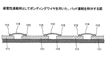
チップ積層の技術について、特許文献1及び特許文献2に掲載されているように、種々の提案がなされているが、その構造及び製造方法が複雑であり、上記の産業界の要求を満たすに至っていない。図1は、従来のチップの積層を例示する図である。複数の半導体チップ11をその集積回路の面12を配線基板13の面に平行にして階段状に積層し、各々の半導体チップ11の縁辺に配置されたパッド14同士及び配線基板13の接続端子15を、ボンディングワイヤ16を用いて接続する。階段状に配置されたパッドを順々にボンディングし、更に基板の接続端子に接続されるボンディングワイヤは、階段状の接続により配線長が長くなるため、電気的特性が低下することがある。また、階段状の積層により、チップ積層体全体の占める面積が大きくなり、十分な高密度の実装製品が得られないことがあった。そして、チップ積層の製造工程が複雑なため、生産性の低下等を生じていた。
Various proposals have been made for chip stacking technology as disclosed in
本発明は、これらの問題点を解決するためになされたものであって、製品品質の向上と工程の簡略化を目的とする。 The present invention has been made to solve these problems, and aims to improve product quality and simplify processes.
本半導体チップ積層体は、接続端子を有する配線基板と、前記配線基板上に積層された複数のチップ封止体と、を有し、それぞれの前記チップ封止体は、半導体集積回路、パッド、及び前記パッドと外部装置とを接続する第1ボンディングワイヤを備えた半導体チップと、前記第1ボンディングワイヤの前記外部装置側の端部を露出するように前記半導体チップの全面を封止する樹脂と、を含み、前記樹脂は、前記半導体チップの集積回路面及び側面並びに前記第1ボンディングワイヤを封止する第1樹脂と、前記半導体チップの集積回路面と反対側の面を封止する第2樹脂と、を含み、前記接続端子と、それぞれの前記チップ封止体の前記第1ボンディングワイヤの前記外部装置側の端部とは、第2ボンディングワイヤを介して導電接続され、前記複数のチップ封止体、前記第2ボンディングワイヤ、及び前記接続端子は、樹脂封止材に封止されていることを要件とする。 The semiconductor chip stack includes a wiring board having connection terminals, and a plurality of chip sealing bodies stacked on the wiring board. Each chip sealing body includes a semiconductor integrated circuit, a pad, And a semiconductor chip having a first bonding wire for connecting the pad and an external device, and a resin for sealing the entire surface of the semiconductor chip so as to expose an end of the first bonding wire on the external device side The resin includes an integrated circuit surface and a side surface of the semiconductor chip, a first resin that seals the first bonding wire, and a second surface that seals a surface opposite to the integrated circuit surface of the semiconductor chip. includes a resin, and a said connecting terminal, and the external device side of the end portion of the first bonding wires for each of the chip sealing body, conductive connection is via a second bonding wire , Wherein the plurality of chips the sealing body, the second bonding wires, and the connection terminal, it is a requirement that is sealed in the resin sealing material.
本半導体チップ積層体の製造方法の一の形態は、半導体集積回路及びパッドを備えた半導体チップとなる複数の領域を有する半導体ウエハにダイシングテープを貼り付け、前記半導体ウエハをダイシングし、前記ダイシングテープ上に所定間隔で配置された複数の半導体チップを作製するダイシング工程と、前記ダイシング工程により得られた個々の前記半導体チップのうち、隣接する前記半導体チップの前記パッド間を第1ボンディングワイヤにより導電接続するパッド接続工程と、前記ダイシングテープ上に、前記半導体チップ及び前記第1ボンディングワイヤを封止する第1樹脂を形成する第1樹脂形成工程と、前記ダイシングテープを剥離する剥離工程と、前記半導体チップ及び前記第1樹脂の前記剥離工程で露出した部分を封止する第2樹脂を形成する第2樹脂形成工程と、隣接する前記半導体チップ間に位置する前記1樹脂、前記第1ボンディングワイヤ、及び前記第2樹脂を切断して、前記第1ボンディングワイヤの端部が前記第1樹脂から露出する複数のチップ封止体を形成するチップ封止体形成工程と、前記複数のチップ封止体を積層し、各々の前記チップ封止体の前記第1樹脂から露出する前記第1ボンディングワイヤの端部同士を第2ボンディングワイヤにより相互に接続してチップ積層体を形成するチップ積層体形成工程と、前記チップ積層体を配線基板上に搭載し、前記チップ積層体と前記配線基板とを封止する第3樹脂を形成する第3樹脂形成工程と、を有することを要件とする。 One form of the manufacturing method of this semiconductor chip laminated body is that a dicing tape is attached to a semiconductor wafer having a plurality of regions to be a semiconductor chip having a semiconductor integrated circuit and a pad, the semiconductor wafer is diced, and the dicing tape A dicing process for producing a plurality of semiconductor chips arranged at predetermined intervals thereon , and among the individual semiconductor chips obtained by the dicing process, the pads between adjacent semiconductor chips are electrically connected by a first bonding wire. A pad connecting step for connecting; a first resin forming step for forming a first resin for sealing the semiconductor chip and the first bonding wire on the dicing tape; a peeling step for peeling the dicing tape; Sealing the semiconductor chip and the exposed portion of the first resin in the peeling step A second resin forming step for forming a second resin, and the end portion of the first bonding wire by cutting the first resin, the first bonding wire, and the second resin located between the adjacent semiconductor chips. from but the chip sealing body forming step that form a plurality of chips sealing body exposed from the first resin, wherein a plurality of stacked chips sealing body, each of said chip sealing body of the first resin said first bonding wire ends chip stack formation step of interconnected to form the chip stack by a second bonding wire which is exposed, mounting the chip stack on a wiring substrate, the chip stack a third resin forming step of forming a third resin for sealing said wiring board and the body, in that it has a requirement.
本半導体チップ積層体の製造方法の他の形態は、半導体集積回路及びパッドを備えた半導体チップとなる複数の領域を有する半導体ウエハをダイシングし、複数の半導体チップを形成するダイシング工程と、前記ダイシング工程により得られた個々の前記半導体チップを、ダイアタッチフィルム上に所定間隔で搭載する半導体チップ搭載工程と、前記ダイアタッチフィルム上に搭載された個々の前記半導体チップのうち、隣接する前記半導体チップの前記パッド間を第1ボンディングワイヤにより導電接続するパッド接続工程と、前記ダイアタッチフィルム上に、前記半導体チップ及び前記第1ボンディングワイヤを封止する樹脂を形成する樹脂形成工程と、隣接する前記半導体チップ間に位置する前記樹脂、前記第1ボンディングワイヤ、及び前記ダイアタッチフィルムを切断して、前記第1ボンディングワイヤの端部が前記樹脂から露出する複数のチップ封止体を形成するチップ封止体形成工程と、前記複数のチップ封止体を積層し、各々の前記チップ封止体の前記樹脂から露出する前記第1ボンディングワイヤの端部同士を第2ボンディングワイヤにより相互に接続してチップ積層体を形成するチップ積層体形成工程と、前記チップ積層体を配線基板上に搭載し、前記チップ積層体と前記配線基板とを配線接続する配線接続工程と、を有することを要件とする。
In another embodiment of the method for producing a semiconductor chip laminate , a semiconductor wafer having a plurality of regions to be a semiconductor chip having a semiconductor integrated circuit and a pad is diced, and a dicing step of forming a plurality of semiconductor chips, and the dicing The semiconductor chip mounting step of mounting the individual semiconductor chips obtained by the steps on the die attach film at predetermined intervals, and the adjacent semiconductor chips among the individual semiconductor chips mounted on the die attach film A pad connecting step of conductively connecting the pads with a first bonding wire; a resin forming step of forming a resin for sealing the semiconductor chip and the first bonding wire on the die attach film; The resin located between the semiconductor chips, the first bonding wire, By cutting fine the die attach film, and the chip sealing body forming step end portion of the first bonding wire that form a plurality of chips sealing body exposed from the resin, the plurality of chips the sealing body stacked, and the chip stack forming step of the ends of the first bonding wire which is exposed from each of the resin of the chip sealing body are connected to each other by the second bonding wire forming a chip stack, wherein mounting the chip stack on a wiring board may be a requirement that having a wiring connection step of wiring connecting the wiring board and the chip stack.
本発明により、高密度実装の形状と工程を実施して、製品品質の向上と工程の簡略化を図ることができる。 According to the present invention, the shape and process of high-density mounting can be performed to improve product quality and simplify the process.
以下、図面を参照して、本発明を実施するための最良の実施の形態を説明する。 The best mode for carrying out the present invention will be described below with reference to the drawings.
(第1の実施の形態)
本発明の第1の実施の形態は、個片化されたチップ封止体の角部が切欠き面を有する、いわゆるベベル形状を有することを特徴とするチップ積層体の例である。
(First embodiment)
The first embodiment of the present invention is an example of a chip laminated body having a so-called bevel shape in which corners of a chip sealing body separated into pieces have a notch surface.
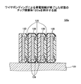
図2は、本発明の第1の実施の形態に係る個片化されたチップ封止体25を例示する図である。半導体チップ21のパッド22に導電性連結材23が連結され、導電性連結材23の外部装置側の端部の先端の面24を除いて、半導体チップ21の全面及び導電性連結材23が樹脂封止されてチップ封止体25が形成されている。半導体チップ21の集積回路面21a及び側面21bは絶縁樹脂26により封止され、半導体チップ21の裏面21cは絶縁樹脂27により封止されている。絶縁樹脂26及び27には、例えば、エポキシ系樹脂等の素材を使用することができる。さらに、絶縁樹脂27には、絶縁と接着の2つの機能を併せ持つダイアタッチフィルムを使用する。ダイアタッチフィルムを使用すると、半導体チップ裏面を樹脂封止することができ、かつ、ダイシング後にチップ封止体を積層する工程において、積層のための接着フィルム貼付又は接着剤塗布等の工程を省略できるので、工程の簡素化を図ることができる。
FIG. 2 is a diagram illustrating a
図3は、本発明の第1の実施の形態に係るチップ封止体の角部に切欠き面31及び32を有するチップ封止体を例示する図である。前出の図2のチップ封止体25の角部28に、切欠き面31及び32が形成され、集積回路面21aに対してなす各度がそれぞれθ1及びφ1の平面である。θ1及びφ1は、チップ封止体の積層の状態における導電性連結材33の形状及びボンディングワイヤ形状の設計条件に応じて、例えば、30度、45度又は60度等の値である。ボンディングワイヤの長手方向に対する切欠き面の傾斜角度を変えて、絶縁樹脂から露出するボンディングワイヤの端部の先端の面の面積が広くなるように設定するためである。特別な条件がなければ、θ1とφ1とを同一の値としてよい。
FIG. 3 is a diagram illustrating a chip sealing body having notched
(第1の実施の形態の効果)
チップ封止体が積層された場合に、電気的特性向上の効果が顕著である。切欠き面の形成によって、ボンディングワイヤの端部の先端の面の面積を広くすることにより、チップ封止体を良好な条件で導電接続することができ、電気的特性を向上させることができる。また、導電性連結材33の先端の面を接続するための導電性のボンディングワイヤが、導電性連結材33の先端の面の接続箇所において接続する際に、つぶれ変形等による拡がり等を生じても、切欠き面31及び32が形成する窪みの空間内に留まる。従って、チップ封止体の側面37から導電性のボンディングワイヤの変形した部分がはみ出すことはなく、パッケージの外形寸法を所定の値に保持できる寸法的効果を有する。
(Effects of the first embodiment)
When the chip sealing body is laminated, the effect of improving electrical characteristics is remarkable. By forming the notch surface, the area of the tip end surface of the bonding wire is widened, whereby the chip sealing body can be conductively connected under favorable conditions, and the electrical characteristics can be improved. Further, when the conductive bonding wire for connecting the front end surface of the conductive connecting
(第1の実施の形態の変形例)
図4は、本発明の第1の実施の形態の変形例に係るチップ封止体の角部に凹形の曲面41を有するチップ封止体を例示する図である。
(Modification of the first embodiment)
FIG. 4 is a diagram illustrating a chip sealing body having concave
(第1の実施の形態の変形例の効果)
導電性連結材とボンディングワイヤの接続箇所において、ボンディングワイヤが変形して拡がりを生じても、凹形の曲面が、平面の切欠き面の場合より大きな空間部分を形成するので、チップ封止体の側面42からボンディングワイヤの変形した部分がはみ出すことがない。従って、パッケージの外形寸法を所定の寸法に、精度よく保つことができる。
(Effects of Modification of First Embodiment)
Even if the bonding wire deforms and expands at the connection point between the conductive connecting material and the bonding wire, the concave curved surface forms a larger space than in the case of the flat cut-out surface. The deformed portion of the bonding wire does not protrude from the
(第1の実施の形態の他の変形例)
本発明の第1の実施の形態の他の変形例は、チップ封止体の上下の角部に切欠き面を設けたチップ封止体である。
(Other modifications of the first embodiment)
Another modification of the first embodiment of the present invention is a chip sealing body in which notched surfaces are provided at upper and lower corners of the chip sealing body.
図5は、本発明の第1の実施の形態の他の変形例に係る上下の角部に切欠き面を設けたチップ封止体50を例示する図である。前述の図3で示したチップ封止体における切欠き面31及び32に加えて、集積回路面の反対側に位置する絶縁樹脂27の側の角部に切欠き面51,52を設ける。切欠き面51及び52の、集積回路面21aに対してなす各度は、それぞれθ2及びφ2である。
FIG. 5 is a diagram illustrating a
(第1の実施の形態の他の変形例の効果)
係る上下の角部に切欠きを有するチップ封止体50を積層すれば、導電性連結材の露出端面を導電性のボンディングワイヤを接続するに際し、接続部分の周辺の空間を広くとることができるので、接続のためのボンディングツールの動作を円滑に行うことができる。従って、ボンディングの工程が簡素化され、また、製品品質を向上させることができる。また、切欠き面を凹形の曲面とした場合にも、同様の効果を上げることができる。
(Effects of other modifications of the first embodiment)
If the
(第2の実施の形態)
本発明の第2の実施の形態は、複数のチップ封止体と、導電性のボンディングワイヤと配線基板とを有するチップ積層体が樹脂封止された半導体チップ積層体である。
(Second Embodiment)
The second embodiment of the present invention is a semiconductor chip stacked body in which a chip stacked body including a plurality of chip sealed bodies, a conductive bonding wire, and a wiring board is sealed with a resin.
図6は、本発明の第2の実施の形態に係る半導体チップ積層体60を例示する図である。チップ封止体61が積層されて、角部の各々の切欠き面62に露出した導電性連結材の端部63が、ボンディングワイヤ64によって接続され、チップ積層体が形成され、チップ積層体は、配線基板65上の接着層66に載置され、ボンディングワイヤ64の端部が配線基板65の接続端子67に接続されている。チップ積層体、配線基板の接続端子及び配線基板は、絶縁樹脂68により封止され、半導体チップ積層体60が形成される。
FIG. 6 is a diagram illustrating a semiconductor chip stacked
配線基板65としては、エポキシ樹脂等の有機材料多層配線基板、またはシリコンを主体とする半導体基板等広い範囲の配線基板を使用することができる。
As the
(第2の実施の形態の効果)
図6に示すような半導体チップ積層体60の形成によって、半導体チップを多段積層したときの積層方向の投影面積を、半導体チップのサイズに近づけることができる。また、チップ封止体の側面に沿って配線するボンディングワイヤを最短の長さにすることができるので、半導体チップ積層体の電気的特性を向上させることができる。
(Effect of the second embodiment)
By forming the semiconductor chip stacked
(第2の実施の形態の応用例1)
本発明の第2の実施の形態の応用例1は、2対のチップ封止体の切欠き面が対向するように積層された半導体チップ積層体である。
(
The application example 1 of the second embodiment of the present invention is a semiconductor chip stacked body that is stacked so that the notch surfaces of two pairs of chip sealing bodies face each other.
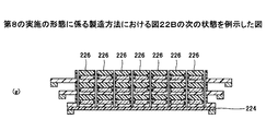
図7は、本発明の第2の実施の形態の応用例1に係る、2対の、切欠き面が対向したチップ封止体と、他の1個のチップ封止体とが積層された半導体チップ積層体70を例示する図である。半導体チップ積層体は、切欠き面71が対向している一対のチップ封止体71a及び71bと、切欠き面72が対向している他の一対のチップ封止体72a及び72bと、他の1個のチップ封止体73を有している。各チップ封止体が積層され、導電接続されてチップ積層体を形成し、チップ積層体が配線基板75の上に積層搭載されて、半導体チップ積層体70を形成する。なお、説明の便宜のため、図7において半導体チップ積層体の全体を封止する樹脂は省いている。
FIG. 7 shows a stack of two pairs of chip sealing bodies facing each other and one other chip sealing body according to the application example 1 of the second embodiment of the present invention. 5 is a diagram illustrating a semiconductor chip stacked
図8は、図7のA部及びB部の拡大図である。チップ封止体71aの切欠き面71が形成する空間74a及び76aの形状が、チップ封止体71bの切欠き面71が形成する空間74b及び76bの形状と、チップ封止体71a及び71bの重ね合わせ面77を対称面とする面対称な形状であることを示している。ただし、切欠き面の集積回路面に対しなす角度に関して、導電接続におけるボンディングツールの動作等に支障がない場合には、面対称でなくともよい。
FIG. 8 is an enlarged view of part A and part B of FIG. The shapes of the
なお、図7及び図8において、ボンディングワイヤはチップ封止体71a及び71bの側面に接している状態を示しているが、必ずしも接触させずに設けることができる。
7 and 8, the bonding wires are in contact with the side surfaces of the
(第2の実施の形態の応用例1の効果)
角部に切欠きを設けたチップ封止体を積層することにより、導電性のボンディングワイヤの接続時に、チップ封止体の接続部分の周辺の空間を広くとることができるので、ボンディングツールの動作を円滑に行うことができ、工程簡素化及び製品品質の向上を図ることができる。また、図8において、導電接続のためのボンディングワイヤ78が、導電性連結材81との接続箇所82において変形による拡がりを生じても、切欠き面71が形成する空間74a,74b,76a及び76bが、係る拡がりの部分を内包することができる。従って、導電性のボンディングワイヤの変形した部分が、チップ封止体の側面79からはみ出すことがなく、パッケージの外形寸法を所定の値に保持できる寸法的効果を有する。
(Effect of application example 1 of the second embodiment)
By laminating chip sealing bodies with cutouts at the corners, the space around the chip sealing body connection area can be widened when connecting conductive bonding wires. Can be performed smoothly, and the process can be simplified and the product quality can be improved. In FIG. 8, even if the
(第2の実施の形態の応用例2)
本発明の第2の実施の形態の応用例2は、2対のチップ封止体の切欠き面が対向するように積層された、他の半導体チップ積層体である。
(Application 2 of the second embodiment)
The application example 2 of the second embodiment of the present invention is another semiconductor chip stacked body in which the notch surfaces of the two pairs of chip sealing bodies are stacked to face each other.
図9は、切欠き面が凹形の曲面である半導体チップ積層体の部分を例示する図であり、前述の図7におけるA部及びB部に相当している。図9は、ボンディングワイヤの導電接続の前の状態を示している。チップ封止体91aの切欠き面91が形成する空間94a及び96aの形状が、チップ封止体91bの切欠き面91が形成する空間94b及び96bの形状と、チップ封止体91a及び91bの重ね合わせ面97を対称面とする面対称な形状であることを示している。なお、ボンディングツールの動作に支障がない場合には、面対称でなくともよい。
FIG. 9 is a diagram illustrating a portion of the semiconductor chip stacked body in which the cut-out surface is a concave curved surface, and corresponds to the A portion and the B portion in FIG. 7 described above. FIG. 9 shows a state before the conductive connection of the bonding wire. The shapes of the
(第2の実施の形態の応用例2の効果)
切欠き面が凹面を形成する応用例2の場合には、上記応用例1の効果を得ると共に、応用例1の平面の切欠き面の場合よりも更に広い空間を確保できるので、応用例1の効果を更に高めることができる。
(Effect of application example 2 of the second embodiment)
In the case of the application example 2 in which the cut surface forms a concave surface, the effect of the application example 1 can be obtained, and a wider space can be secured than in the case of the flat cut surface of the application example 1. This effect can be further enhanced.
(第3の実施の形態)
本発明の第3の実施の形態に係る発明は、半導体チップ積層体の製造方法である。
(Third embodiment)
The invention according to the third embodiment of the present invention is a method for manufacturing a semiconductor chip laminate.
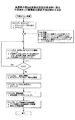
図10は、本発明の第3の実施の形態に係る半導体チップ積層体の製造方法のステップを例示する図である。各製造ステップにおける製品の形態を例示した図11(a)〜図13Bを参照して、図10の製造方法のステップを説明する。 FIG. 10 is a diagram illustrating the steps of the method for manufacturing a semiconductor chip stacked body according to the third embodiment of the invention. The steps of the manufacturing method of FIG. 10 will be described with reference to FIGS. 11A to 13B illustrating the form of the product in each manufacturing step.
(ステップ1.ダイシング)
図11(a)は、準備すべき半導体ウエハ110を例示する図である。外径が6インチ、8インチ又は12インチの半導体ウエハに110にダイシングテープを貼り付け、ダイサ装置に装着後、個々の半導体チップに分離する。ウエハの厚さは、例えば50μmである。パッケージ製品の設計条件に応じて、予め所定の寸法に加工されている。
(
FIG. 11A is a diagram illustrating a
図11(b)は、半導体ウエハ110がダイサ装置(図示せず)により個々の半導体チップ111に分離された状態を例示する図である。このとき、ダイシングテープ112は、切断されることなく、かつテープの接着力によって、個々の半導体チップ111を、ダイサ装置のブレードによる切り代d1の間隔で配置された状態に保持することができる。ブレードによる切り代d1は、例えば50μmである。
FIG. 11B is a diagram illustrating a state in which the
本発明のチップ積層体に使用されるチップ封止体の樹脂封止については、半導体チップの相互の絶縁性確保のため、十分な樹脂封止が必要であり、特に半導体チップの側面は十分な絶縁材の厚さを要する。そこで、本発明は、切り代d1に加えて、半導体チップ同士の十分な分離間隔を設定するための手段を提供している。 With respect to the resin sealing of the chip sealing body used in the chip stack of the present invention, sufficient resin sealing is necessary to ensure mutual insulation between the semiconductor chips, and particularly the side surface of the semiconductor chip is sufficient. Insulating material thickness is required. Therefore, the present invention provides means for setting a sufficient separation interval between the semiconductor chips in addition to the cutting allowance d1.
(ステップ2.チップ封止体形成)
ステップ2.a)半導体チップ間隔設定において、ダイシングテープの縁辺部分をダイシングリングにより保持し半径方向の外側へ引張り拡大させ、即ちダイシングテープのエキスパンドによって、半導体チップの分離間隔を拡げる。このエキスパンドは、ダイシングリングに保持されたダイシングテープをエキスパンダ装置に装着して実施することができる。半導体チップの分離間隔は、通常100μm〜200μmとし、また、封止の条件によっては更に広く、100μmとすることができる。
(Step 2. Formation of chip sealing body)
Step 2. a) In setting the semiconductor chip interval, the edge portion of the dicing tape is held by the dicing ring and pulled outward in the radial direction, that is, the separation interval of the semiconductor chips is expanded by expanding the dicing tape. This expansion can be performed by attaching a dicing tape held on a dicing ring to the expander device. The separation interval of the semiconductor chips is usually 100 μm to 200 μm, and can be further widened to 100 μm depending on the sealing conditions.
ステップ2.b.パッド連結において、チップ封止体同士の導電接続の接続部を形成するため、半導体チップの上のパッド同士を、導電性連結材を用いて連結する。 Step 2. b. In pad connection, pads on the semiconductor chip are connected to each other using a conductive connecting material in order to form a conductive connection portion between the chip sealing bodies.
図11(c1)は、導電性連結材としてボンディングワイヤを用いた、パッド連結を例示する図である。(ステップ2.チップ封止体形成)のa)半導体チップ間隔設定において間隔が分離された半導体チップ111の上のパッド113同士を、ボンディング装置(図示せず)を用いて、ボンディングワイヤ114によって連結する。ボンディングワイヤの直径は、通常、20μm〜30μmであるが、接続を容易にする等の目的で、より大きい直径を使用することができる。連結されたボンディングワイヤの頂点の高さは、半導体チップの集積回路面から40μmの高さである。導電性連結材の材質は、金、アルミニウム、銅、タングステンまたはそれらの合金である。また、ボンディングワイヤの他にボンディングリボンを使用することができる。パッド連結されたボンディングワイヤの形状は、図11(c1)に示すような、上に凸のなだらかな曲線であるが、図11(c2)に示すように、ボンディングワイヤを横から見た形状が、英文字のM字形となるよう、ワイヤボンディングの動作を制御することができる。すなわち、「ボンディングの接続点の間のボンディングワイヤを含む面内におけるボンディングワイヤの形状が、少なくとも1個の凹部を有する曲線となるように形成」することができる。
FIG. 11C1 is a diagram illustrating pad connection using a bonding wire as the conductive connection material. (Step 2. Chip sealing body formation) a) The
なお、ステップ2.において、a)半導体チップ間隔設定(ダイシングテープ引張り拡大)と、b)パッド連結の順序を入れ替えて、パッド連結を先に行ってから、ダイシングテープ引張り拡大を行うことができる。この場合には、パッド連結後にダイシングテープ引張り拡大を行うことにより、パッド間を繋ぐワイヤも同時に引張られるので、ワイヤの高さが下がり、封止体の高さを低くすることが可能である。 Step 2. In (a), the semiconductor chip interval setting (dicing tape tension expansion) and b) the pad connection order are changed, and after the pad connection is performed first, the dicing tape tension expansion can be performed. In this case, by performing the dicing tape pulling expansion after connecting the pads, the wires connecting the pads are also pulled at the same time, so that the height of the wires can be lowered and the height of the sealing body can be lowered.
ステップ2.c)集積回路面、側面及び導電性連結材の樹脂封止において、絶縁樹脂を用いて、チップ封止体を形成する。ボンディングワイヤ等の導電性連結材が封止されて、次のステップ3で導電接続されるべき接続点の位置に固定される。
Step 2. c) In resin sealing of the integrated circuit surface, side surfaces, and conductive connecting material, a chip sealing body is formed using an insulating resin. A conductive connecting material such as a bonding wire is sealed and fixed at a position of a connection point to be conductively connected in the
図11(d)は、チップ封止体形成における、集積回路面、側面及び導電性連結材の樹脂封止の状態を例示する図である。ダイシングテープ112に載置された状態の半導体チップが樹脂封止され、半導体チップの集積回路面115、側面116及び導電性連結材のボンディングワイヤ114が絶縁樹脂116bで封止された状態を示す。絶縁樹脂の材料は、フィルム状樹脂又は液状樹脂等を使用する。フィルム状樹脂は、シリカまたはアルミナをフィラーとして含んだエポキシ樹脂を使用することができる。集積回路面、側面及び導電性連結材の全体を、加熱等により軟化した樹脂で封止し、導電性連結材の撓み状態を保ちつつ硬化させる。その他、液状樹脂としてポリイミド樹脂を用いて、チップ樹脂封止を行うことができる。封止する樹脂の厚さd2は50μmのレベルである。
FIG. 11D is a diagram illustrating a state of resin sealing of the integrated circuit surface, the side surface, and the conductive connecting material in the formation of the chip sealing body. The semiconductor chip placed on the dicing
ステップ2.d)半導体チップ裏面樹脂封止において、一群のチップ封止体が形成される。半導体チップ裏面の樹脂封止を行うために、裏面に密着しているダイシングテープを剥離する。ダイシングテープ112は、ステップ2.のa)半導体チップ間隔設定の工程から、c)集積回路面、側面及び導電性連結材の樹脂封止の工程に至るまでの間、半導体ウエハから分離した各半導体チップ111を保持していた。ダイシングテープ112を剥離し、半導体チップの裏面を図11(e)に示す絶縁樹脂117bにより封止し、半導体チップの全面が封止される。絶縁樹脂として、ダイアタッチフィルムを使用する。
Step 2. d) In the semiconductor chip backside resin sealing, a group of chip sealing bodies is formed. In order to perform resin sealing on the back surface of the semiconductor chip, the dicing tape that is in close contact with the back surface is peeled off. The dicing
ダイアタッチフィルムは、絶縁性を有しかつ接着の機能を有するので、絶縁樹脂層として半導体チップ裏面樹脂封止に使用することができる。予め半導体チップ裏面の封止樹脂の表面に接着の機能をもたせることができるので、チップ封止体個片化後に行うチップ封止体積層の工程において、ダイアタッチフィルム貼付又は接着剤塗布等の工程を省くことができる。 Since the die attach film has an insulating property and an adhesion function, it can be used as an insulating resin layer for sealing a semiconductor chip back surface resin. Since the surface of the sealing resin on the back surface of the semiconductor chip can have a bonding function in advance, in the process of stacking the chip sealing body after the chip sealing body is separated, a process such as die attach film application or adhesive application Can be omitted.
また、他の製造方法としては、絶縁樹脂として上記の集積回路面115及び側面116等を封止した場合と同様に、フィルム状樹脂、液状樹脂又はタブレット状のエポキシ樹脂等を使用することができる。樹脂の厚さd3は、例えば50μmである。
As another manufacturing method, a film-like resin, a liquid resin, a tablet-like epoxy resin, or the like can be used as in the case where the
ステップ2.e)チップ封止体個片化において、半導体チップ積層体に用いられるチップ封止体を形成する。このため、チップ封止体の個片化用のダイシングテープを準備する。 Step 2. e) In the chip sealing body singulation, a chip sealing body used for a semiconductor chip stacked body is formed. For this reason, a dicing tape for individualizing the chip sealing body is prepared.
図11(e)は、半導体チップ裏面樹脂封止を終えた一群のチップ封止体にチップ封止体の個片化用のダイシングテープが貼付された状態を例示する図である。チップ封止体の個片化用のダイシングテープ119を、樹脂封止された一群のチップ封止体118の裏面に貼付し、ダイサ装置用のフレーム(図示せず)に固定する。
FIG. 11E is a diagram illustrating a state in which a dicing tape for separating the chip sealing body is attached to a group of chip sealing bodies after the semiconductor chip back surface resin sealing is completed. A dicing
なお、ダイシングテープの使用に際して、絶縁樹脂の性質を有するダイアタッチフィルムが積層された構造を有するダイシングテープを使用することができる。即ち、図11(e)において、ダイアタッチフィルム117bがダイシングテープ119に積層されている状態のテープを改めて準備し、裏面が樹脂封止されていない一群のチップ封止体の裏面に貼付し、樹脂封止する。係るダイアタッチフィルムが積層されたダイシングテープを使用することにより、従来のダイシングテープ(図11(d)に示す112)剥離後の半導体チップ裏面樹脂封止及び積層のための接着剤塗布の工程を、上述の積層したダイシングテープの119の部分のみを剥離することにより、簡素化できる。従って、次に示すステップ2.e)チップ封止体個片化及びステップ3.a)チップ封止体積層の工程を一層簡素化することができる。
In addition, when using a dicing tape, the dicing tape which has the structure where the die attach film which has the property of insulating resin was laminated | stacked can be used. That is, in FIG. 11 (e), a tape in which the die attach
ステップ2.e)チップ封止体個片化において、一群のチップ封止体118をダイサ装置により個片化し、半導体チップ積層体に用いられるチップ封止体を得る。
Step 2. e) In the chip sealing body singulation, the group of
図11(f)は、一群のチップ封止体から個片化されたチップ封止体120を例示する図である。ただし、ダイシングテープを省いて示している。個片化されたチップ封止体同士の間隔は、例えば20μm〜30μmである。次に、ベベルカット用ブレード等を装着したダイサ装置(図示せず)を用いて、チップ封止体の角部の切欠き面121を形成する。この切欠き面121における導電性連結材の端部の露出面が、導電性連結材の長手方向122に対し傾斜角度θ3を有するので、導電性のボンディングワイヤとの接続面を広くとることができ、良好な電気的特性を有することができる。切欠き面の角度は、導電性連結材の設計形状、樹脂厚さ等の設計条件に応じて選択する。また、複数のブレードを使用するデュアルダイシング等の方法により、効率的なチップ封止体のダイシングを実施することができる。
FIG. 11F is a diagram illustrating a
(ステップ3.導電接続)
チップ封止体を積層し、各チップ封止体同士の導電接続を行う。
(
The chip sealing bodies are stacked and conductive connection between the chip sealing bodies is performed.
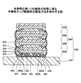
ステップ3.a)チップ封止体積層において、複数の封止チップを積層し相互に固定する。ステップ2.d)半導体チップ裏面樹脂封止において、ダイアタッチフィルムを絶縁樹脂として使用しているので、接着層等を新たに設けることなく複数の封止チップを積層することができる。また、絶縁樹脂層がダイアタッチフィルムの機能を有していない場合には、別の接着層としてのダイアタッチフィルム等を貼付し、チップ封止体を積層する。
図11(g)は、別の接着層を設けた場合の、チップ封止体の積層が終了した状態を例示する図である。チップ積層用架台123を利用して、上記のステップ2.e)チップ封止体個片化において個片化されたチップ封止体120を積層して、チップ積層体を形成する。各チップ封止体は、厚さ10μm〜100μmのダイアタッチフィルム124によって、厚さ方向に相互に接着固定される。チップ積層体の一辺の寸法は、8mm〜10mmである。
FIG. 11G is a diagram illustrating a state where stacking of the chip sealing body is completed when another adhesive layer is provided. Using the
ステップ3.b.導電接続において、各々のチップ封止体の表面から露出した各々の導電性連結材の端部を、導電性のボンディングワイヤにより接続する。
図12は、ワイヤボンディングによる導電接続が終了した状態のチップ積層体120aを例示する図である。ボンディングワイヤの材質は、金、アルミニウム、銅、タングステンまたはそれらの合金である。アルミニウムを使用する場合には、その外径は通常100μm以下であり、常温でのボンディングが可能である。積層されたチップ封止体の表面に露出した導電性のボンディングワイヤの端部を、連続一括してボンディングすることができる。
FIG. 12 is a diagram illustrating the chip stacked
チップ封止体の切欠き面に露出する導電性連結材の端部を接続するためのボンディングワイヤは、切欠き面に沿って設けられるので、側面からみた形状が、少なくとも1個の凹部125を有する曲線となる。ボンディングワイヤの凹部125の形状と切欠き面の形成する窪んだ空間に、ボンディングワイヤの接続箇所における変形による拡がり部分が内包されて、チップ封止体の側面からボンディングワイヤがはみ出すことがない。従って、チップ積層体の外形寸法を所定の値に保持することができ、パッケージ製品としての寸法精度を上げることができる。
Since the bonding wire for connecting the end portion of the conductive connecting material exposed to the notch surface of the chip sealing body is provided along the notch surface, the shape viewed from the side surface has at least one
(ステップ4.チップ積層体樹脂封止)
a)チップ積層体の配線基板搭載を行い、チップ積層体と配線基板について、b)樹脂封止を行う。
(Step 4. Chip laminate resin sealing)
a) A chip stack is mounted on a wiring board, and b) resin sealing is performed on the chip stack and the wiring board.
図13Aは、チップ積層体の配線基板搭載を完了した状態を例示する図である。樹脂封止の形状も合わせて示した。ここに、チップ積層体120aの配線基板搭載とは、複数のチップ封止体120が、積層され一体となったチップ積層体120aが、配線基板131の上に固定され、配線基板との間に導電接続を行う実装方法を指している。導電接続は、ボンディングワイヤ133の端部134の長さを調整して、配線基板131の接続端子135との距離を予め見込んだ長さに切断することにより、容易に行うことができる。ダイアタッチフィルムを絶縁樹脂として使用しているので、接着層等を設けることなく複数の封止チップを積層することができる。
FIG. 13A is a diagram illustrating a state in which the mounting of the chip stack on the wiring board is completed. The shape of resin sealing is also shown. Here, the mounting of the
また、チップ封止体の積層順序等の設計条件に応じて、チップ封止を順次に配線基板の上に積み重ねた後に、チップ封止体同士の導電接続を行ってもよい。 In addition, according to design conditions such as the stacking order of the chip sealing bodies, the chip sealing bodies may be sequentially stacked on the wiring substrate, and then the conductive connection between the chip sealing bodies may be performed.
図13Bは、チップ積層体の配線基板搭載を完了した他の状態を例示する図である。複数のチップ封止体120が積層され一体となったチップ積層体120aが、配線基板131の上に置かれ、接着層132によって固定されている。
FIG. 13B is a diagram illustrating another state in which the mounting of the chip stack on the wiring board is completed. A chip laminated
なお、それぞれのチップ封止体の有する集積回路の面の向きについて、一方向に向きを揃えてチップ封止体を積層するか、集積回路の面を対向させて、複数の対のチップ封止体を積層するかの選択は、チップ積層体全体の設計条件に合わせて行うことができる。ただし、向きを変えたチップ封止体の積層については、積層する毎に個々の接着樹脂形成が必要である。 In addition, as for the direction of the surface of the integrated circuit that each chip sealing body has, a plurality of pairs of chip sealing are performed by stacking the chip sealing bodies in one direction or by stacking the chip surfaces facing each other. The choice of whether to stack the bodies can be made in accordance with the design conditions of the entire chip stack. However, regarding the stacking of the chip sealing bodies whose directions are changed, it is necessary to form individual adhesive resins each time they are stacked.
次に、配線基板搭載の終了したチップ積層体と配線基板について、b.樹脂封止を行い、半導体チップ積層体を得る。 Next, with respect to the chip stack and the wiring board that have been mounted on the wiring board, Resin sealing is performed to obtain a semiconductor chip laminate.
前出の図6は、得られた半導体チップ積層体について、トランスファーモールド法による樹脂封止の形態を例示している。他にポッティング樹脂等を使用したサイドフィルによる樹脂封止も可能である。 FIG. 6 described above exemplifies the form of resin sealing by transfer molding for the obtained semiconductor chip stack. In addition, resin sealing by side fill using potting resin or the like is also possible.
(第3の実施の形態の効果)
ダイシングテープの引張り拡大と切欠き面の形成によって、工程の簡略化と電気的特性等の製品品質の向上を図ることができる。
(Effect of the third embodiment)
Simplification of the process and improvement of product quality such as electrical characteristics can be achieved by expanding the tension of the dicing tape and forming the notched surface.
(第3の実施の形態の変形例)
本発明の第3の実施の形態の変形例は、半導体チップ積層体の他の製造方法である。半導体チップ積層体を構成するチップ封止体に関して、切欠き面を形成しない他の方法を用いることによっても、電気的特性を劣化させることなく、半導体チップ積層体を形成することができる。
(Modification of the third embodiment)
A modification of the third embodiment of the present invention is another method for manufacturing a semiconductor chip stacked body. With respect to the chip sealing body constituting the semiconductor chip stacked body, the semiconductor chip stacked body can be formed without deteriorating electrical characteristics by using another method that does not form a notch surface.
図14Aは、本発明の第3の実施の形態の変形例に係る他の製造方法により形成された半導体チップ積層体140を例示する図である。前述の(第3の実施の形態)の(ステップ2.チップ封止体形成)における図11(c2)に示したように、ボンディングワイヤの、連結パッド間の中央部に凹部を有する、いわゆる英文字のM字形の形状を顕著に形成する場合は、チップ封止体の角部の切欠き面の形成をすることなく、導電接続できる。その理由は、図14Aにおいて、絶縁樹脂面におけるボンディングワイヤ141の端部の先端の面142が、ボンディングワイヤの長手方向X−Xと傾斜角度θ4を有することにより、楕円のような広い面となり、広い接続面を形成するので、次の(ステップ3.導電接続)におけるボンディングが、容易にかつ十分に行えるからである。なお、上記「英文字のM字形」は、図11(c2)に示されているように、連結パッドの間のボンディングワイヤを含む面内におけるボンディングワイヤの形状に着目したとき、少なくとも1個の凹部を有する曲線となるように形成されることを指す表現である。
FIG. 14A is a diagram illustrating a semiconductor chip stacked
(第3の実施の形態の変形例の効果)
導電性連結材としてのボンディングワイヤの連結された形状が、少なくとも1個の凹部を有する曲線であるときには、チップ封止体の切欠き面を設けずに、導電性連結材の露出端部の面の広い面積を確保でき、連結部の電気的特性の向上を図ることができる。また、工程の簡素化を図ることができる。
(Effects of Modification of Third Embodiment)
When the connected shape of the bonding wire as the conductive connecting material is a curve having at least one recess, the surface of the exposed end of the conductive connecting material without providing the notch surface of the chip sealing body A large area can be secured, and the electrical characteristics of the connecting portion can be improved. In addition, the process can be simplified.
(第3の実施の形態の応用例)
本発明の第3の実施の形態の応用例は、外部接続端子を有する複数の半導体チップ積層体の製造方法である。
(Application example of the third embodiment)
An application example of the third embodiment of the present invention is a method for manufacturing a plurality of semiconductor chip laminates having external connection terminals.
図14Bは、本発明の第3の実施の形態の応用例に係る半導体チップ積層体の製造方法のステップを例示する図である。第3の実施の形態の製造方法を示した前出の図10のステップと異なるのは、(ステップ4A.チップ積層体樹脂封止)以降の工程である。 FIG. 14B is a diagram illustrating steps in a method for manufacturing a semiconductor chip stacked body according to an application example of the third embodiment of the present invention. What is different from the above-described step of FIG. 10 showing the manufacturing method of the third embodiment is the process after (Step 4A. Chip laminated body resin sealing).
図14Cは、本発明の第3の実施の形態の応用例に係る外部接続端子を有する複数の半導体チップ積層体を例示する図である。図14Cを参照して製造方法のステップを説明する。ただし、(ステップ1.ダイシング)から(ステップ3.導電接続)までの各ステップは、第3の実施の形態について図10に示したステップと同様であるので、説明を省く。
FIG. 14C is a diagram illustrating a plurality of semiconductor chip stacks having external connection terminals according to an application example of the third embodiment of the present invention. The steps of the manufacturing method will be described with reference to FIG. 14C. However, since each step from (
(ステップ4A.チップ積層体樹脂封止)
a)において、複数のチップ積層体120aを共通の配線基板144の上に搭載して、b)において、配線基板144と共に絶縁樹脂145により封止し、樹脂封止した半導体チップ積層体146を形成する。
(Step 4A. Chip laminate resin sealing)
In a), a plurality of chip laminated
(ステップB.樹脂封止チップ積層体外部端子接続)
a)金属バンプ載置、b)リフローによって、金属バンプ等の外部接続端子147を接続する。金属バンプには、スズ,銀等のはんだ又は銅コアボールのはんだ等の材料を選択することができる。
(Step B. External terminal connection of resin-encapsulated chip laminate)
(ステップC.チップ積層体パッケージ個片化)
配線基板の個片化すべき位置148をシャー装置等により分離切断して、パッケージ製品が得られる。
(Step C. Separate chip stack package)
A package product can be obtained by separating and cutting the
(第3の実施の形態の応用例の効果)
外部接続端子を有する複数のチップ積層体のパッケージを同時に製造することにより、生産性の向上を図ることができる。
(Effects of application example of third embodiment)
By simultaneously manufacturing a package of a plurality of chip stacks having external connection terminals, productivity can be improved.
(第4の実施の形態)
本発明の第4の実施の形態は、前述の第3の実施の形態の製造方法に示した図10のステップ2.e)チップ封止体個片化から、ステップ3.a)チップ封止体積層にかけての製造工程の、他の製造方法に関するものである。一群のチップ封止体の個片化に際して使用すべきダイシングテープを置き換えて、ダイシングテープの機能を有するダイアタッチフィルムを使用することを特徴とする、半導体チップ積層体の製造方法である。
(Fourth embodiment)
The fourth embodiment of the present invention is the same as step 2 in FIG. 10 shown in the manufacturing method of the third embodiment. e) From chip sealing body singulation,
図15Aは、本発明の第4の実施の形態に係る半導体チップ積層体の製造方法を例示する図である。一群のチップ封止体150の個片化に際し、ダイシングテープに替えて、チップ封止体の保持等を行うダイシングテープの機能及びチップ積層時のダイアタッチの接着機能の、2つの機能を併せ持つダイアタッチフィルム151を使用する。ダイアタッチフィルム151は、チップ封止体150に接着し、また、ダイアタッチフィルム151の裏面には接着層152が設けられ、接着層152は、テープ基材157により保護されている。ダイアタッチフィルム151が貼り付けられたチップ封止体150を、ダイシングした後、テープ基材157から剥がして、個片化したチップ封止体が得られる。チップ封止体はダイアタッチ層を有しているので、個片化後直ちに、チップ封止体の積層を行うことができる。なお、テープ基材157の材料としては、ポリオレフィン、ポリエチレンテレフタート、ポリプロピレン等を使用することができる。
FIG. 15A is a diagram illustrating the method for manufacturing the semiconductor chip stacked body according to the fourth embodiment of the invention. When the group of
(第4の実施の形態の効果)
チップ封止体の個片化・積層において、従来行っていたダイアタッチフィルムの貼り付け加工とチップ封止体の個片化用のダイシングテープの貼り付け加工とを、同時に行うことができるので、工程の簡略化を図ることができる。
(Effect of the fourth embodiment)
In chip-separated chip stacking / lamination, the conventional die attach film pasting process and chip sealing body dicing tape pasting process can be performed simultaneously, The process can be simplified.
(第5の実施の形態)
本発明の第5の実施の形態は、前述の第3の実施の形態の製造方法に示した図10のステップ2.e)チップ封止体個片化から、ステップ3.a)チップ封止体積層にかけての製造工程に関する、さらに他の製造方法である。一群のチップ封止体の個片化用ダイシングテープの裏面に接着層を設けることを特徴とする。
(Fifth embodiment)
The fifth embodiment of the present invention is the same as step 2 in FIG. 10 shown in the manufacturing method of the third embodiment. e) From chip sealing body singulation,
図15Bは、本発明の第5の実施の形態に係る半導体チップ積層体の製造方法を例示する図である。一群のチップ封止体150の面153に貼付されるチップ封止体の個片化用のダイシングテープ154は、チップ封止体150との接着面の反対側の面155に、接着層156を有する。チップ封止体の個片化用のダイシングテープ154にダイアタッチの機能を併せ持たせて、チップ封止体の積層を行う。すなわち、ダイシングテープ154は、チップ封止体150をダイシングする際に、チップ封止体150の全体を固定し、個々のチップ封止体のピックアップ時まで、チップ封止体を保持するとともに、次の積層の工程において、接着層156によって、チップ封止体の積層におけるダイアタッチの機能を有する。ダイシングテープ154の接着層156の側は、テープ基材158によって保護されている。ダイシングテープ154が貼り付けられたチップ封止体150を、ダイシングした後、テープ基材158から剥がして、個片化したチップ封止体が得られる。チップ封止体は接着層を有しているので、直ちにチップ封止体の積層を行うことができる。なお、テープ基材158の材料としては、ポリオレフィン、ポリエチレンテレフタート、ポリプロピレン、塩化ビニル等を使用することができる。
FIG. 15B is a diagram illustrating the method for manufacturing the semiconductor chip stacked body according to the fifth embodiment of the invention. The dicing
(第5の実施の形態の効果)
ダイアタッチフィルムに関する第4の実施の形態の効果と同様に、個片化・チップ積層において、従来行っていたダイアタッチフィルムの貼り付け加工とチップ封止体の個片化用のダイシングテープ貼り付け加工とを、同時に行うことができるので、工程の簡略化を図ることができる。
(Effect of 5th Embodiment)
Similar to the effect of the fourth embodiment relating to the die attach film, in the singulation and chip stacking, the pasting process of the die attach film and the pasting of the dicing tape for singulation of the chip sealing body are performed. Since the processing can be performed at the same time, the process can be simplified.
(第6の実施の形態)
本発明の第6の実施の形態は、チップ積層体の最下層の半導体チップが、配線基板にフリップチップ実装されていることを特徴とする半導体チップ積層体である。
(Sixth embodiment)
The sixth embodiment of the present invention is a semiconductor chip laminate in which the lowermost semiconductor chip of the chip laminate is flip-chip mounted on a wiring board.
図16は、本発明の第6の実施の形態に係る半導体チップ積層体160を例示する図である。構造と製造方法は以下の通りである。図は、配線基板との接続面と対向する最下層の半導体チップ161が、配線基板162とフリップチップ接続している場合のチップ積層体を示している。最下層の半導体チップ161は、配線基板162と接続バンプ163によりフリップチップ接続され、その他のチップ封止体164は、ボンディングワイヤ165によってチップ封止体同士が導通されている。半導体チップ161のフリップチップ接続後、配線基板162との間隙をアンダーフィル166により封止する。半導体チップ161の背面にダイアタッチフィルム167を設けて、その上に他のチップ封止体のチップ積層体を積層する。チップ積層体と配線基板との導通のため、チップ積層体の側面に設けられたボンディングワイヤ165と配線基板162の接続端子169とを接続する。配線基板との接続の際、ボンディングワイヤ165の端部170の長さを調整して、配線基板165の接続端子169との距離を予め見込んだ長さに切断しておけば、ボンディングを容易に行うことができる。更に配線基板への外部接続端子の接続も可能である。その場合の製造方法は、(第3の実施の形態の応用例)の半導体チップ積層体の製造方法において示した図14Bの(ステップ4A.チップ積層体樹脂封止)以降と同様の方法を使用する。
FIG. 16 is a diagram illustrating a semiconductor chip stacked
(第6の実施の形態による効果)
最下層の半導体チップが多端子を有している場合にも、配線基板と接続させて、半導体チップ積層体を形成することができる。上層に載置されるチップ積層体と組合わせることによって、本発明の半導体チップ積層体の形態を利用できる半導体チップの種類を拡大することができ、複合半導体としての機能拡張に貢献することができる。例えば、多端子のロジック回路のCPUとメモリの半導体チップの積層等を実現することができる。
(Effects of the sixth embodiment)
Even when the lowermost semiconductor chip has multiple terminals, it can be connected to a wiring board to form a semiconductor chip stack. By combining with the chip stack placed on the upper layer, the types of semiconductor chips that can utilize the form of the semiconductor chip stack of the present invention can be expanded, contributing to functional expansion as a composite semiconductor. . For example, a multi-terminal logic circuit CPU and memory semiconductor chip can be stacked.
(第7の実施の形態)
本発明の第7の実施の形態は、ダイシングした半導体チップをダイアタッチフィルム(DAF)上の一定の位置に移載して行う半導体チップ積層体の製造方法である。前述の第3の実施の形態においては、半導体チップ同士の分離間隔を設定するため、ダイシングテープの引張り拡大(エキスパンド)の方法を使用したが、第7の実施の形態は、ダイシングした半導体チップを、ダイアタッチフィルム(DAF)上の一定の位置に搭載する手段を用いる。
(Seventh embodiment)
The seventh embodiment of the present invention is a method for manufacturing a semiconductor chip laminate, in which a diced semiconductor chip is transferred to a certain position on a die attach film (DAF). In the above-described third embodiment, the method of expanding the dicing tape (expanding) is used to set the separation interval between the semiconductor chips. However, in the seventh embodiment, a diced semiconductor chip is used. A means for mounting at a certain position on the die attach film (DAF) is used.
図17は、本発明の第7の実施の形態に係る半導体チップ積層体の製造方法を例示する図である。 FIG. 17 is a diagram illustrating a method for manufacturing a semiconductor chip stacked body according to the seventh embodiment of the invention.
製造方法は、(ステップ1.ダイシング)、(ステップ2A.チップ封止体形成)、(ステップ3A.導電接続)及び(ステップ4A.チップ積層体の配線接続)の各ステップを有して、半導体チップ積層体が製造される。以下、図17の製造方法を、ステップの順を追って、図18A〜図18Dの各ステップにおける半導体チップの状態を例示する図を参照しながら、説明する。
The manufacturing method includes the steps of (
(ステップ1.ダイシング)
半導体ウエハのダイシングにより個々の半導体チップを得るダイシング工程については、前出の第3の実施の形態における状態と同様であるので、説明を省く。
(
The dicing process for obtaining individual semiconductor chips by dicing the semiconductor wafer is the same as the state in the third embodiment described above, and will not be described.
(ステップ2A.チップ封止体形成)
当ステップは、ピックアップした半導体チップが、DAF上の一定の位置に搭載され、パッド連結され、半導体チップ全体等が樹脂封止され、更に樹脂封止されたチップ封止体が個別化される工程である。図18Aの(a)から図18Cの(g)が、上記のチップ封止体の個別化までの工程を示している。
(Step 2A. Chip encapsulant formation)
This step is a process in which the picked-up semiconductor chip is mounted at a fixed position on the DAF, pad-connected, the entire semiconductor chip or the like is resin-sealed, and the resin-sealed chip sealing body is individualized. It is. FIG. 18A (a) to FIG. 18C (g) show the steps from the above-described individualization of the chip sealing body.
(ステップ2A. a.半導体チップピックアップ、DAF上の一定位置に搭載、DAF仮貼り付け)
図18Aの(a)は、ダイシングテープ上の半導体ウエハが、ダイシングを終えた状態を示している。ダイシングを終えた個々の半導体チップ181は、ダイソーの切り代の間隔d1のままダイシングテープ182に置かれている。係る状態の半導体チップ181をピックアップして、新たに準備したダイアタッチフィルム上の、所定の位置に搭載する。
(Step 2A. A. Semiconductor chip pickup, mounted at a fixed position on DAF, DAF temporarily pasted)
FIG. 18A (a) shows a state in which the semiconductor wafer on the dicing tape has been diced. The
図18Aの(b)は、所定の位置に搭載された半導体チップ181の状態を示している。ダイアタッチフィルム183への搭載の所定の位置は、半導体チップの側面の樹脂封止による封止代と、封止後のチップ封止体個片化におけるダイサ装置のブレードによる切り代(例えば25μm〜30μm)から算定した、各半導体チップの位置である。搭載に際しては、光学的装置を用いた位置設定機構を用いて、十分な搭載位置の精度を確保することができる。
FIG. 18A (b) shows the state of the
ダイアタッチフィルム183の機能は、チップ封止体の積層における接着層の機能、封止樹脂として半導体チップの絶縁性確保及び機械的保護の機能である。半導体チップの半導体集積回路側の面の反対側の面である裏面側は、封止樹脂の機能を有するダイアタッチフィルムによって封止された状態となる。ダイアタッチフィルム183の材料は、例えば日立化成工業(株)製DF402の系統、リンテック(株)製LE5000の系統又は東レ(株)製WL−NCFの系統等を使用する。半導体チップ181との仮貼り付けの条件は、例えば80〜100℃の温度で10秒の時間を要する。半導体チップの封止において、特に半導体チップのコーナー部における封止材の密着性が重要で、製品品質に影響を与える。ダイアタッチフィルム183の、半導体チップが仮貼り付けされる面と反対側の面には、表面の保護等のためのテープ基材183Aが設けられている。なお、テープ基材183Aの材料としては、ポリオレフィン、ポリエチレンテレフタート、ポリプロピレン等を使用することができる。
The function of the die attach
図18Aの(c)は、仮貼り付けされた半導体チップの状態を示している。仮貼り付け時に、樹脂が流動し、半導体チップ181の下方側面184に密着して、半導体チップと確実に密着した封止状態を形成する。
FIG. 18A (c) shows a state of the temporarily attached semiconductor chip. At the time of temporary attachment, the resin flows and adheres to the
(ステップ2A. b.パッド連結(ワイヤボンディング))
図18Bの(d)は、パッドが連結された状態を示している。パッド連結の形態は、各半導体チップを隔てている溝181aを跨ぐ形態である。係る跨ぐ形態を必要とするのは、2段階先のチップ封止体個片化(ステップ2A.のd.(図17))において、ボンディングワイヤを、ダイシングされた後の樹脂表面に露出させ、さらに導電接続するためである。樹脂表面における露出部分を広い面積として、(ステップ3A.のb.(図17))において精度よく導電接続することができる。また、パッド連結の形状は、図18Bの(d)に示すような上に凸の形状に限ることなく、ボンディングワイヤを横から見た形状が、例えば英文字のM字形をなすように制御して形成することができる。
(Step 2A.b. Pad connection (wire bonding))
FIG. 18B (d) shows a state in which the pads are connected. The form of pad connection is a form straddling the
図18Bの(e)は、ボンディングワイヤ185を横から見た形状が英文字のM字形であることを例示する図である。図11(c2)と同様に、「ボンディングの接続点の間のボンディングワイヤを含む面内におけるボンディングワイヤの形状が、少なくとも1個の凹部を有する曲線となるように形成」することができる。係るボンディングワイヤの形状を維持することによって、チップ封止体を積層して導電接続を行う際に、チップ封止体の角部の切欠き面を設けることなく、ボンディングワイヤの、導電部材との接続面を広い面積にして、導電接続を容易にかつ高い精度で行うことができる。前出の(第3の実施の形態の変形例)においても、同様の効果を示した。
(E) of FIG. 18B is a figure which illustrates that the shape which looked at the
(ステップ2A. c.集積回路面、側面及び導電性連結材の樹脂封止)
図18Bの(f)は、集積回路面、側面及び導電性連結材の樹脂封止によって、一群のチップ封止体186が形成された状態を例示する図である。半導体チップ181の裏面付近187は、既に、樹脂封止の機能を有するダイアタッチフィルム183によって封止されているので、半導体チップの未封止部分及びボンディングワイヤ(一般的には導電性連結材)を樹脂封止することによって半導体チップ及びボンディングワイヤの封止が終了する。
(Step 2A. C. Resin sealing of integrated circuit surface, side surface and conductive connecting material)
FIG. 18B is a diagram illustrating a state in which a group of
このステップ2Aのc.において封止に使用される樹脂180は、仮貼り付け時には、低粘度の物性であることを要する。導電接続を容易にかつ高い精度で行うために、ボンディングワイヤの軸の封止端面とのなす角度を、一定の角度に保つ必要から、樹脂封止する際、ボンディングワイヤの、上に凸の形状又はM字形等(図18Bの(d),(e))を維持する必要があるからである。例えば東レ(株)のWL―NCF等は、仮貼り付け時に低粘度の物性を有し、使用することができる。ボンディングワイヤの軸の封止端面とのなす角度を、一定の角度に保つ必要についての説明は、(第3の実施の形態の変形例)において、図14Aを用いて説明した。
In step 2A, c. The
(ステップ2A. d.チップ封止体個片化)
一群のチップ封止体186(図18Bの(f))をダイサ装置(図示せず)により個片化し、半導体チップ積層体に用いられるチップ封止体を得る。
(Step 2A. D. Chip sealing body singulation)
A group of chip sealing bodies 186 ((f) in FIG. 18B) is separated into pieces by a dicer device (not shown) to obtain a chip sealing body used for a semiconductor chip stacked body.
図18Cの(g)は、一群のチップ封止体186から個片化されたチップ封止体188を例示する図である。個片化されたチップ封止体同士の間隔は、例えば20μm〜30μmである。チップ封止体188は、次の積層の工程において、保護用のテープ基材183Aから剥がされ、ダイアタッチフィルム183を介して積層される。ダイサ装置のブレードに平歯を使用した場合には、図18Cの(g)に示すような角部が直角をなす断面のチップ封止体が形成される。
FIG. 18C is a diagram illustrating a
(チップ封止体の角部に切欠き面を形成する他の方法)
チップ封止体の封止樹脂の表面のボンディングワイヤの露出部分に関して、その面積を広くする他の方法として、前出の(第3の実施の形態)において示したように、ダイサ装置にベベルカット用ブレードを用いて、チップ封止体の角部に切欠き面を形成することができる。すなわち、ステップ2Aのd.において、切欠き面を更に形成する方法である。その場合には、図11(f)の各部の符号を説明のために使用すると、切欠き面121における導電性連結材(ボンディングワイヤ)の端部の露出面が、導電性連結材の長手方向122に対し傾斜角度θ3を有するので、導電接続のための導電性のボンディングワイヤとの接続面を広くとることができ、良好な電気的特性を有することができる。また、(第3の実施の形態)と同様に、複数のブレードを使用するデュアルダイシング等の方法により、効率的なチップ封止体のダイシングを実施することができる。
(Other methods for forming a notch surface at the corner of the chip sealing body)
As another method for widening the area of the exposed portion of the bonding wire on the surface of the sealing resin of the chip sealing body, as shown in the above (third embodiment), the dicer device is bevel-cut. A notch surface can be formed at the corner of the chip sealing body using the blade for manufacturing. That is, d. In this method, a notch surface is further formed. In that case, when the reference numerals of the respective parts in FIG. 11 (f) are used for explanation, the exposed surface of the end portion of the conductive connecting material (bonding wire) on the
(ステップ3A.導電接続)
(ステップ3A.a.チップ封止体積層)
チップ封止体を積層し、各チップ封止体同士の導電接続を行う。複数の封止チップを積層し相互に固定する。
(Step 3A. Conductive connection)
(Step 3A.a. Chip Encapsulant Lamination)
The chip sealing bodies are stacked and conductive connection between the chip sealing bodies is performed. A plurality of sealing chips are stacked and fixed to each other.
図18Cの(h)はチップ封止体積層が終了した状態を例示する図である。架台190上において、チップ封止体188が接着樹脂層のダイアタッチフィルム183を介して積層され、チップ積層体189が形成される。
(H) of FIG. 18C is a diagram illustrating a state in which the chip sealing body lamination is completed. On the
(ステップ3A.b.導電接続(ワイヤボンディング))
各々のチップ封止体の表面に露出した各々の導電性連結材の端部を、導電性のボンディングワイヤにより接続する。
(Step 3A.b. Conductive connection (wire bonding))
End portions of the respective conductive coupling members exposed on the surfaces of the respective chip sealing bodies are connected by conductive bonding wires.
図18Dの(i)は、ワイヤボンディングの接続法による導電接続が終了した状態のチップ積層体191を例示する図である。ボンディングワイヤ192の材質は、金、アルミニウム、銅、タングステンまたはそれらの合金である。アルミニウムを使用する場合には、その外径は通常100μm以下であり、常温でのボンディングが可能である。積層されたチップ封止体188の表面に露出したボンディングワイヤ(導電性連結材)193の端面194を、ワイヤボンダ装置(図示せず)を用いて連続一括してボンディングすることができる。導電接続されたボンディングワイヤの形状は、図のようにチップ封止体の封止樹脂側面から離れていても、また接触していてもよい。ボンディングワイヤ192の端部195は、配線基板との配線接続のための端子となる部分である。
FIG. 18D is a diagram illustrating the
(ステップ4A.チップ積層体の配線接続)
チップ積層体と配線基板との配線接続がパッケージ組み立ての最終工程となり、パッケージ製品が完成する。半導体チップが積層されたパッケージの製品は、配線基板を介して電子機器に搭載される。
(Step 4A. Wiring connection of chip laminated body)
Wiring connection between the chip stack and the wiring board is the final process of package assembly, and the package product is completed. A package product in which semiconductor chips are stacked is mounted on an electronic device via a wiring board.
図18Dの(j)は、チップ積層体の配線接続が終了した状態を例示する図である。 (J) of FIG. 18D is a diagram illustrating a state where the wiring connection of the chip stack is completed.
(ステップ4A.a.チップ積層体の基板への載置)
導電接続を終了したチップ積層体191が配線基板197に載置され、ダイアタッチフィルム196により接着固定される。
(Step 4A.a. Placement of chip stack on substrate)
The chip laminated
(ステップ4A.b.基板と配線接続)
図18Dの(j)において、ボンディングワイヤの端部195と配線基板197の接続端子198とが配線接続された状態を示している。以上で半導体チップ積層体の製造が終了する。
(Step 4A.b. Wiring connection with substrate)
FIG. 18D (j) shows a state in which the
(第7の実施の形態の効果)
第1の効果は、製品品質、歩留まりの向上である。製造工程において、KGD(Known Good Die)についての特別な選別工程を設けることなく、KGDのみの半導体チップ積層体のパッケージを製造することができる。
(Effect of 7th Embodiment)
The first effect is an improvement in product quality and yield. In the manufacturing process, it is possible to manufacture a package of a semiconductor chip stack of only KGD without providing a special screening process for KGD (Known Good Die).
半導体のパッケージ工程として、ウエハの寸法のまま半導体チップの集合を扱うことができるウエハレベルパッケージ(WLP)の製造工程は、量産的効果を有し、また品質向上に極めて効果的である。ウエハ全体に配置された半導体チップを、連続する一体品としてパッケージを製造することができるからである。しかし、ウエハ上に配置された半導体チップの中には、検査により不良品と認定されたものが含まれるので、パッケージ後の配線基板への実装に際して、不良品については除去しておく手段、工程が、一般には必要である。しかし、第7の実施の形態に係る製造方法によれば、ステップ2A.のa.の半導体チップピックアップ時に、KGDのみをピックアップしてダイアタッチフィルム上に搭載することができるので、不良品除去のための特別な選別工程を設けることなく、KGDのみを用いたパッケージを製造することができる。従って、製品品質、歩留まりの向上を図ることができる。 As a semiconductor packaging process, a wafer level package (WLP) manufacturing process capable of handling a set of semiconductor chips with the dimensions of a wafer has a mass production effect and is extremely effective in improving quality. This is because a package can be manufactured by using semiconductor chips arranged on the entire wafer as a continuous integrated product. However, since the semiconductor chips arranged on the wafer include those certified as defective by inspection, means and processes for removing defective products when mounted on the wiring board after packaging. However, it is generally necessary. However, according to the manufacturing method according to the seventh embodiment, step 2A. A. Since only KGD can be picked up and mounted on the die attach film when picking up the semiconductor chip, a package using only KGD can be manufactured without providing a special sorting step for removing defective products. it can. Therefore, it is possible to improve product quality and yield.
第2の効果は、製品品質、寸法精度の向上である。ステップ2A.のa.において、KGDの半導体チップ181をピックアップして、新たに準備したダイアタッチフィルム183上の、所定の位置に、光学的機器等を使用して搭載する。樹脂封止の封止代、チップ封止体個片化時のダイサ装置のブレード等の数値に基づいて設定した搭載の位置の精度を確保することによって、チップ封止体の寸法精度を向上させることができる。また、半導体チップの側面の封止樹脂の厚さについて、使用環境のニーズに合わせて自由に高精度に製作することができる。従って、ダイシングテープを引張り拡大してチップ封止体を製造する方法等と比較して、一層の製品品質の向上を図ることができる。
The second effect is improvement of product quality and dimensional accuracy. Step 2A. A. The
第3の効果は、工程の簡略化である。樹脂封止の機能を有するダイアタッチフィルムを使用することにより、チップ封止体の積層に際して、改めて積層のための接着層を設ける工程を実施することなく、チップ封止体全体の積層固定を実施することができるので、製造工程を簡略化することができる。 A third effect is simplification of the process. By using a die attach film that has a resin sealing function, the entire chip sealing body can be stacked and fixed without performing the process of providing an adhesive layer for stacking again when stacking the chip sealing body. Therefore, the manufacturing process can be simplified.
(第7の実施の形態の応用例)
配線基板と配線接続されたチップ積層体の使用条件によっては、次の図19に示すステップ4B.のような、チップ積層体に樹脂封止を施す製造方法が必要となる。
(Application example of seventh embodiment)
Depending on the use conditions of the chip laminate connected to the wiring board by wiring, Step 4B. Thus, a manufacturing method for applying resin sealing to the chip stack is required.
図19は、本発明の第7の実施の形態の応用例に係る半導体チップ積層体の製造方法を例示する図である。 FIG. 19 is a diagram illustrating a method for manufacturing a semiconductor chip stacked body according to an application example of the seventh embodiment of the invention.
本製造方法は、(ステップ1.ダイシング)、(ステップ2A.チップ封止体形成)、(ステップ3A.導電接続)、(ステップ4A.チップ積層体の配線接続)及び(ステップ4B.チップ積層体樹脂封止)の工程を有している。前出の(第7の実施の形態)におけるチップ積層体の配線接続を終了した状態に加えて、更にチップ積層体及び配線基板を樹脂封止する「チップ積層体樹脂封止工程」を特徴とする半導体チップの製造方法である。本製造方法の各ステップについて、前出の第7の実施の形態の場合との重複する説明を省き、(ステップ4B.チップ積層体樹脂封止)について説明する。
This manufacturing method includes (
(ステップ4B.チップ積層体樹脂封止)
図20は、(ステップ4B.チップ積層体樹脂封止)の樹脂封止を終えたチップ積層体の状態を例示する図である。封止樹脂201によって、配線接続を終えたチップ積層体191及び配線基板197が樹脂封止された状態である。樹脂封止の方法については、トランスファーモールド法又はポッティング法等を選択する。
(Step 4B. Chip laminate resin sealing)
FIG. 20 is a diagram illustrating a state of the chip laminated body after the resin sealing in (Step 4B. Chip laminated body resin sealing) is completed. The chip laminated
(第7の実施の形態の応用例の効果)
チップ積層体全体が樹脂封止されているので、係るチップ積層体の応用製品が、機械的、化学的に厳しい環境において使用された場合であっても、その環境に耐え得る高度の品質を提供することができる。
(Effects of application example of seventh embodiment)
Since the entire chip stack is sealed with resin, even if the applied product of the chip stack is used in a harsh mechanical and chemical environment, it provides a high quality that can withstand that environment. can do.
(第8の実施の形態)
本発明の第8の実施に係る発明は、「平面を形成する一群のチップ封止体を一括積層した後に個片化する」点において、「チップ封止体を個片化後に積層する」第3〜7の実施の形態に係る製造方法の発明と異なる。固定枠に設けられたDAF(ダイアタッチフィルム)を使用し、DAF上の複数の半導体チップに対して、パッド連結及び封止を行うことによって、枠付きDAF上のチップ封止体の集合を複数形成した後、光学的位置合わせ機構等を使用して、枠ごと積層し、チップ封止体の全体が硬化した後に、ダイシングして、個々のチップ積層体を得ることを特徴とする。
(Eighth embodiment)
The invention according to the eighth embodiment of the present invention is that "a group of chip sealing bodies forming a plane are separated after being collectively laminated" and "a chip sealing body is laminated after being separated" It differs from the invention of the manufacturing method according to the third to seventh embodiments. Using a DAF (die attach film) provided on a fixed frame and performing pad connection and sealing with respect to a plurality of semiconductor chips on the DAF, a plurality of chip sealing bodies on the DAF with a frame are assembled. After the formation, the entire frame is stacked using an optical alignment mechanism or the like, and after the entire chip sealing body is cured, dicing is performed to obtain individual chip stacks.
図21は、本発明の第8の実施の形態に係る半導体チップ積層体の製造方法を例示する図である。 FIG. 21 is a diagram illustrating a method for manufacturing the semiconductor chip stacked body according to the eighth embodiment of the invention.
製造方法は、(ステップ1.ダイシング)、(DAF準備)、(ステップD1.枠付きDAF上のチップ封止体形成)、(ステップE.一括積層)、(ステップF.チップ封止体個片化)、(ステップG.導電接続)及び(ステップH.チップ積層体の配線接続)の各ステップを有して、半導体チップ積層体が製造される。
The manufacturing methods are (
図22A〜図22Cは、第8の実施の形態に係る製造方法における各状態を例示した図である。以下、図22A〜図22Cの各状態の図を参照しながら、図21に示した製造方法を、ステップの順を追って説明する。 22A to 22C are diagrams illustrating each state in the manufacturing method according to the eighth embodiment. Hereinafter, the manufacturing method illustrated in FIG. 21 will be described in the order of steps with reference to the respective states of FIGS. 22A to 22C.
(ステップ1.ダイシング)
第7の実施の形態その他で示したダイシングと同様であるので、本ステップの説明を省く。
(
Since this is the same as the dicing shown in the seventh embodiment and others, the description of this step is omitted.
(DAF準備)
ダイアタッチフィルム(DAF)をSUS枠に貼付した状態のものを、チップ封止体の積層数の数だけ、N層分準備する。SUS枠は、製造工程にて変質、変形を生じない材料でできた固定枠であればよい。最下層に相当するSUS枠貼付のDAFに関してのみは、ダイシングテープを貼り付けた上にDAFを積層した状態で準備する。最下層のDAFは、積層したチップ封止体を個片化する時に必要となる。また、積層するための位置合わせマークを、各SUS枠に、又はDAF面に設けておく。
(DAF preparation)
N die-attach films (DAF) in a state in which they are pasted on a SUS frame are prepared for N layers by the number of stacked chip sealing bodies. The SUS frame may be a fixed frame made of a material that does not change or deform in the manufacturing process. Only for the DAF with the SUS frame attached corresponding to the lowermost layer, the DAF is prepared in a state where the DAF is laminated on the dicing tape. The lowermost DAF is required when the stacked chip sealing bodies are separated. In addition, alignment marks for stacking are provided on each SUS frame or on the DAF surface.
(ステップD.枠付きDAF上のチップ封止体形成)
(ステップD. a.半導体チップピックアップ、SUS枠付きDAF上の一定位置に搭載、仮貼り付け)
図22Aの(a)は、ダイシングされた半導体チップ221がピックアップされて、SUS枠222に貼り付けられたダイアタッチフィルム223上の一定位置に載置された配列状態を示している。半導体チップの半導体集積回路側の面の反対側の面である裏面側は、封止樹脂の機能を有するDAFによって封止された状態となる。半導体チップの配列は、例えば、3行×7列、3行×10列等、半導体チップの寸法、チップ封止体全体の寸法、チップ封止体個片化等の各条件により、決定する。
(Step D. Formation of chip sealing body on DAF with frame)
(Step D. a. Semiconductor chip pickup, mounted at a fixed position on DAF with SUS frame, temporarily attached)
22A shows an arrangement state in which the diced
(ステップD. b.パッド連結(ワイヤボンディング))
チップ封止体の導電接続に使用されるボンディングワイヤを半導体チップ上のパッドに連結する。連結方法及び連結の形態は、(第7の実施の形態)等と同様である。
(Step D.b. Pad connection (wire bonding))
Bonding wires used for conductive connection of the chip sealing body are coupled to pads on the semiconductor chip. The connection method and the form of connection are the same as those in the seventh embodiment.
図22Aの(b)は、パッド連結後の状態を示している。 FIG. 22A (b) shows a state after pad connection.
(ステップD1. c.集積回路面、側面及び導電性連結材の樹脂封止)
図22Bの(c)は、集積回路面、側面及び導電性連結材(ボンディングワイヤ)の樹脂封止後の状態を示している。パッド連結及び集積回路面樹脂封止に関しては、(第7の実施の形態)のステップ2A.の説明と重複するので、説明を省く。
(Step D1. C. Resin sealing of integrated circuit surface, side surface and conductive connecting material)
FIG. 22B (c) shows a state after the resin sealing of the integrated circuit surface, the side surface, and the conductive connecting material (bonding wire). Regarding pad connection and integrated circuit surface resin sealing, step 2A of (seventh embodiment). The description is omitted because it overlaps with the description.
図22Bの(d)及び(e)は、それぞれ、第2層及び第3層のチップ封止体の樹脂封止後の状態を示している。第8の実施の形態においては、チップ封止体の積層数を3層とした例を示しているので、図22Bの(e)に示す最下層となる第3層のチップ封止体の最下面には、(DAF準備)において準備したダイシングテープ224が設けられている。図22Bの(c)から(e)の各図に示されたSUS枠225a,225b,225cの寸法については、次の一括積層時における相互干渉による積層の妨げを防ぐため、外側の幅の寸法W1o,W2o,W3o及び内側の幅の寸法W1i,W2i,W3iのうち、W1i,W2o,W2i,W3oについて、次の数式(A22)を満たす必要がある。SUS枠の縦の寸法についても同様の関係を満たす必要がある。
(D) and (e) of Drawing 22B have shown the state after resin sealing of the chip sealing body of the 2nd layer and the 3rd layer, respectively. In the eighth embodiment, an example in which the number of stacked chip sealing bodies is three is shown, and therefore the third layer chip sealing body, which is the lowermost layer shown in FIG. A dicing
W1i>W2o,W2i>W3o. (A22)
積層の数が増加する場合にも、係る関係と同様の関係を保つことによって、積層を円滑に行うことができる。
W1i> W2o, W2i> W3o. (A22)
Even when the number of stacks increases, stacking can be performed smoothly by maintaining the same relationship as that.
(ステップE.一括積層)
各層を構成するチップ封止体が、SUS枠上のダイアタッチフィルムに搭載されたまま一括積層される工程である。
(Step E. Batch lamination)
This is a step in which the chip sealing bodies constituting each layer are stacked together while being mounted on the die attach film on the SUS frame.
図22Bの(f)は、係る一括積層が終了した状態を示している。積層に際しては、封止樹脂の物性に応じて、一括積層の加圧条件、熱硬化条件を設定する。また、積層における各層同士の位置合わせに際しては、光学的機構及び位置制御システムを使用して、その位置精度を確保する。 FIG. 22B (f) shows a state where the collective stacking has been completed. At the time of lamination, pressurization conditions and thermosetting conditions for batch lamination are set according to the physical properties of the sealing resin. Moreover, when aligning each layer in a lamination | stacking, the positional accuracy is ensured using an optical mechanism and a position control system.
(ステップF.チップ封止体個片化)
チップ封止体の内部にある半導体チップが、縦横に配列されたままで積層された状態、すなわち、半導体チップがマトリックス状になったチップ封止体の集合体を、ダイサ装置を用いて、一括して個片化する工程である。チップ封止体個片化のダイシングに際しては、寸法精度を確保するため、光学的機構及び位置制御システムを使用する。
(Step F. Chip sealing body singulation)
A state in which the semiconductor chips inside the chip sealing body are stacked while being arranged vertically and horizontally, that is, an assembly of chip sealing bodies in which the semiconductor chips are arranged in a matrix form, using a dicer device. This is a process of separating into individual pieces. When dicing the chip sealing body into individual pieces, an optical mechanism and a position control system are used to ensure dimensional accuracy.
図22Cの(g)は、チップ封止体個片化が終了した状態を示している。個片化された各チップ封止体226が、各々間隔を保持して、ダイシングテープ224の上にある。
(G) of FIG. 22C has shown the state which chip | tip sealing body singulation was complete | finished. Each
(ステップG.導電接続)
ダイシングテープ(図22Cの(g)の224)上の個片化された各チップ封止体226をピックアップして、導電接続を行う。係る導電接続及び次の(ステップH.チップ積層体の配線接続)に関しては、(第7の実施の形態)その他で示した工程の内容と同様であるので、説明を省く。以上の工程によって、前出の図18Dの(j)に示されたような、配線接続が終了したチップ積層体を得ることができる。
(Step G. Conductive connection)
Each
また、配線接続を終了したチップ積層体の樹脂封止も可能である。(第7の実施の形態の応用例)において図20に示したように、配線接続を終了したチップ積層体及び配線基板を樹脂封止してもよい。 In addition, resin sealing of the chip stack after completing the wiring connection is also possible. As shown in FIG. 20 in (Application Example of Seventh Embodiment), the chip laminated body and the wiring board that have been connected to each other may be resin-sealed.
(第8の実施の形態の効果)
第8の実施の形態においては、個片化の工程について、チップ封止体の積層後に一括して個片化を行うことにより、(第7の実施の形態)に対して、チップ封止体個片化のダイシングの回数が大幅に減少し、工程の簡略化と製品品質の向上を図ることができる。
(Effect of 8th Embodiment)
In the eighth embodiment, the chip sealing body is separated from the (seventh embodiment) in the individualization step by performing individualization after the chip sealing body is stacked. The number of times of dicing into individual pieces can be greatly reduced, and the process can be simplified and the product quality can be improved.
(第8の実施の形態の変形例)
本発明の第8の実施の形態の変形例は、2層の樹脂層を有するダイアタッチフィルムを用いることにより一括して封止積層する製造方法である。物性の異なる2層の樹脂層を有するダイアタッチフィルムを用いて、パッド連結のボンディングワイヤ側等の封止と半導体チップの裏面付近、すなわち、半導体集積回路側の面の反対側の面付近の封止とを、一括積層時に同時に行う製造方法である。パッド連結に使用されているボンディングワイヤ部分等を封止する樹脂には、低粘度を維持する封止樹脂を要するため、所定の低粘度の物性を有する樹脂層を積層した2層のダイアタッチフィルムを準備する。
(Modification of the eighth embodiment)
A modification of the eighth embodiment of the present invention is a manufacturing method in which a die attach film having two resin layers is used for collectively sealing and laminating. Using a die attach film having two resin layers having different physical properties, sealing on the bonding wire side of the pad connection and the vicinity of the back surface of the semiconductor chip, that is, the surface on the opposite side of the surface on the semiconductor integrated circuit side This is a manufacturing method in which stopping is performed simultaneously during batch lamination. Since the resin for sealing the bonding wire portion used for pad connection requires a sealing resin that maintains a low viscosity, a two-layer die attach film in which resin layers having predetermined low viscosity properties are laminated Prepare.
図23は、本発明の第8の実施の形態の変形例に係る半導体チップ積層体の製造方法を例示する図である。 FIG. 23 is a diagram illustrating a method for manufacturing a semiconductor chip stacked body according to a modification of the eighth embodiment of the invention.
製造方法は、(ステップ1.ダイシング)、(DAF準備)、(ステップD2.枠付きDAF上のチップ封止体形成)、(ステップE2.一括積層)、(ステップF.チップ封止体個片化)、(ステップG.導電接続)及び(ステップH.チップ積層体の配線接続)の各ステップを有して、半導体チップ積層体が製造される。
The manufacturing method is (
図24A及び図24Bは、第8の実施の形態の変形例に係る製造方法における各状態を、順を追って例示した図である。製造方法の一部分のステップは、前出の(第8の実施の形態)における製造方法のステップと同様の部分を含むので、特に異なるステップについて説明し、説明の重複を避ける。 24A and 24B are diagrams sequentially illustrating each state in the manufacturing method according to the modified example of the eighth embodiment. Since the steps of a part of the manufacturing method include the same parts as the steps of the manufacturing method in the above (eighth embodiment), different steps will be described in particular to avoid duplication of description.
(第8の実施の形態の変形例)においては、使用するダイアタッチフィルムが、物性が異なる2層の樹脂層を有することにより、仮貼り付け、樹脂硬化等の製造条件設定及びその効果が異なる点が、1層のダイアタッチフィルムを使用する(第8の実施の形態)と大きく異なっている。 In (variation of the eighth embodiment), the die attach film to be used has two resin layers having different physical properties, so that the production condition setting such as temporary attachment and resin curing and the effect thereof are different. The point is greatly different from using a single-layer die attach film (eighth embodiment).
(ステップ1.ダイシング)
前出の第7の実施の形態その他で示したダイシングと同様であるので、説明を省く。
(
Since this is the same as the dicing shown in the seventh embodiment and others, the description is omitted.
(DAF準備)
積層の層数分のSUS枠に貼り付けたダイアタッチフィルムを準備する。
(DAF preparation)
The die attach film stuck on the SUS frame for the number of laminated layers is prepared.
(DAF準備 a.)
最上層に位置するチップ封止体層に相当する部分の半導体集積回路側及びパッド連結のボンディングワイヤ側等を封止するため、「樹脂フィルム2」のみをSUS枠に貼り付けたものを準備する。この「樹脂フィルム2」とは、低粘度性の物性を有する封止樹脂のフィルムを指し、その使用の理由は、以下の通りである。
(DAF preparation a.)
In order to seal the semiconductor integrated circuit side, the pad connection bonding wire side, and the like in the portion corresponding to the chip sealing body layer located in the uppermost layer, a material in which only “resin film 2” is attached to the SUS frame is prepared. . The “resin film 2” refers to a sealing resin film having low viscosity properties, and the reason for its use is as follows.
後工程の(ステップE2.一括封止積層)においてチップ封止体を形成する際、フィルム状の封止樹脂がパッド連結に使用されているボンディングワイヤに接したときに、ボンディングワイヤの形状を変形させることなく、上に凸の形状又はM字形等を維持したままで封止できるよう、フィルムの仮貼り付け時に低粘度の物性を維持する樹脂フィルムが必要である。このような低粘度の物性を有する樹脂を「樹脂フィルム2」とする。 When forming the chip sealing body in the subsequent process (Step E2. Batch sealing lamination), the shape of the bonding wire is deformed when the film-shaped sealing resin contacts the bonding wire used for pad connection. Therefore, there is a need for a resin film that maintains low-viscosity physical properties when temporarily attached to the film so that the film can be sealed while maintaining an upwardly convex shape or M-shape. The resin having such a low viscosity property is referred to as “resin film 2”.
図24Aの(a)は、チップ封止体の積層の最上層に設けられる「樹脂フィルム2」242がSUS枠243aに貼付された状態を示している。
FIG. 24A (a) shows a state in which “resin film 2” 242 provided in the uppermost layer of the stack of chip sealing bodies is attached to the
(DAF準備 b.)
半導体チップの裏面付近を封止するダイアタッチフィルム本体を「樹脂フィルム1」とし、係る「樹脂フィルム1」と「樹脂フィルム2」の2種のフィルムを積層したフィルムを、第2層以下のチップ封止体に対し、ダイアタッチフィルムとして準備する。
(DAF preparation b.)
The die attach film body that seals the vicinity of the back surface of the semiconductor chip is referred to as “
図24Aの(b)は、「樹脂フィルム2」242の上に「樹脂フィルム1」241が積層された状態のダイアタッチフィルムが、SUS枠243bに貼付された状態を示している。ダイアタッチフィルムの材料は、例えば日立化成工業(株)製DF402の系統、リンテック(株)製LE5000の系統又は東レ(株)製WL−NCFの系統等から選択することができる。また、東レ(株)のWL―NCF等は、仮貼り付け時に低粘度の物性を維持することができ、「樹脂フィルム2」として使用することができる。
FIG. 24A (b) shows a state where the die attach film in which the “
(DAF準備 c.)
チップ積層体の個片化のため、ダイシングテープを準備し、その上に「樹脂フィルム1」を貼り付けた状態のSUS枠付きダイアタッチフィルムを準備する。
(DAF preparation c.)
A dicing tape is prepared for individualization of the chip laminated body, and a die attach film with a SUS frame in a state where “
(ステップD2.枠付きDAF上のパッド連結)
ボンディングワイヤを用いたパッド連結は、(第8の実施の形態)等と同様である。
(Step D2. Pad connection on DAF with frame)
The pad connection using the bonding wire is the same as that in the eighth embodiment.
図24Aの(c)は、(ステップ1.ダイシング)を終えた半導体チップが、ピックアップされて、ステップ2A.のa.のSUS枠に貼付されたダイアタッチフィルム上の一定位置に搭載された状態を示している。
(C) of FIG. 24A shows that the semiconductor chip that has finished (
図24Bの(d)は、SUS枠243bに貼付されたダイアタッチフィルム上でパッド連結を終了した半導体チップの状態を示している。図24Bの(d)に示す層は、最上層のチップ封止体となる。
(D) of FIG. 24B has shown the state of the semiconductor chip which complete | finished pad connection on the die-attach film stuck on the
図24Bの(e)は、最上層の直下の第2層となる層について、そのパッド連結が終了した状態を示している。SUS枠243cの寸法は、最上層のチップ封止体用のSUS枠243bと比較して、干渉することがないように小さい寸法となっている。
(E) of FIG. 24B has shown the state which the pad connection was complete | finished about the layer used as the 2nd layer right under the uppermost layer. The size of the
図24Bの(f)は、最下層となる層について、そのパッド連結が終了した状態を示している。この例においては、第3層が最下層である。SUS枠243dの寸法は、第2層のチップ封止体用のSUS枠243cと比較して、干渉することがないように小さい寸法となっている。
FIG. 24B (f) shows a state in which the pad connection is completed for the lowermost layer. In this example, the third layer is the lowest layer. The size of the SUS frame 243d is smaller than the
以上におけるSUS枠の寸法の関係は、SUS枠243a、243b,243c,243dの外側の幅の寸法U1o,U2o,U3o,U4o及び内側の幅の寸法U1i,U2i,U3i,U4iのうち、U1i,U2o,U2i,U3o,U3i,U4oについて、次の数式(A24)を満たす必要がある。SUS枠の縦の寸法についても同様の関係を満たす必要がある。 The relationship between the dimensions of the SUS frame is as follows: the outer width dimensions U1o, U2o, U3o, U4o and the inner width dimensions U1i, U2i, U3i, U4i of the SUS frames 243a, 243b, 243c, 243d. For U2o, U2i, U3o, U3i, and U4o, it is necessary to satisfy the following equation (A24). The same relationship needs to be satisfied for the vertical dimension of the SUS frame.
U1i>U2o,U2i>U3o、U3i>U4o (A24) U1i> U2o, U2i> U3o, U3i> U4o (A24)
(ステップE2.一括封止積層)
SUS枠の使用によって、多数の半導体チップの樹脂封止及び積層を一括して行うステップである。
(Step E2. Batch sealing lamination)
This is a step of performing resin sealing and stacking of a large number of semiconductor chips at once by using the SUS frame.
図24Bの(g)は、(ステップE2.一括封止積層)が終了した状態を示している。図24A,図24Bの各状態(a),(d),(e)及び(f)に示されたSUS枠で支持された樹脂フィルム、半導体チップ及びボンディングワイヤが、同時に一時に封止積層されている。 (G) of FIG. 24B has shown the state which (step E2. Collective sealing lamination | stacking) completed. The resin film, semiconductor chip, and bonding wire supported by the SUS frame shown in each of the states (a), (d), (e), and (f) of FIGS. 24A and 24B are simultaneously sealed and laminated at the same time. ing.
次の3ステップ;
(ステップF.チップ封止体個片化)
(ステップG.導電接続)
(ステップH.チップ積層体の配線接続)
の工程は、第8の実施の形態における工程と同様であるので、重複を避け、説明を省く。以上によって、第8の実施の形態の変形例である「2層を有するダイアタッチフィルムを用いた一括封止積層」を行うチップ積層体の製造方法が終了する。
また、配線接続を終了したチップ積層体の樹脂封止も可能である。(第7の実施の形態の応用例)において図20に示したように、配線接続を終了したチップ積層体及び配線基板を樹脂封止してもよい。
The next three steps;
(Step F. Chip sealing body singulation)
(Step G. Conductive connection)
(Step H. Wiring connection of chip stack)
Since this process is the same as the process in the eighth embodiment, the description is omitted and the description is omitted. With the above, the chip stacked body manufacturing method for performing “batch sealing lamination using a die attach film having two layers”, which is a modification of the eighth embodiment, is completed.
In addition, resin sealing of the chip stack after completing the wiring connection is also possible. As shown in FIG. 20 in (Application Example of Seventh Embodiment), the chip laminated body and the wiring board that have been connected to each other may be resin-sealed.
(第8の実施の形態の変形例の効果)
2層を有するダイアタッチフィルムを用いることによって、半導体チップの裏面付近以外の封止、すなわちパッドを連結しているボンディングワイヤ部分及び半導体チップの半導体集積回路面と側面等を封止するための個別の封止の工程を設けることなく、全体の一括封止積層の工程において同時に一回で封止及び積層を実施することができるので、工程の簡略化を図ることができる。
(Effect of Modification of Eighth Embodiment)
By using the die attach film having two layers, sealing other than the vicinity of the back surface of the semiconductor chip, that is, the bonding wire portion connecting the pads and the semiconductor integrated circuit surface and the side surface of the semiconductor chip are individually sealed. Since the sealing and laminating can be carried out at the same time in the entire collective sealing and laminating step without providing the sealing step, the process can be simplified.
(第9の実施の形態)
図25は、本発明の第9の実施の形態に係る、チップ積層体250の最下層の半導体チップ251の、配線基板197へのフリップチップ実装を特徴とする半導体チップ積層体260を例示する図である。図25の(a)及び(b)は、樹脂封止材263の形状のみが相違している。
(Ninth embodiment)
FIG. 25 is a diagram illustrating a semiconductor chip stacked
ここで、フリップチップ実装とは、半導体チップの能動素子面を配線基板の接続端子面に対向させ、半導体チップ及び配線基板の端子同士をバンプ等によって直接接続する技術を指す。接続箇所に、アンダーフィル等による封止を施す場合もある。 Here, the flip chip mounting refers to a technique in which the active element surface of the semiconductor chip is opposed to the connection terminal surface of the wiring board, and the terminals of the semiconductor chip and the wiring board are directly connected by bumps or the like. In some cases, the connection location is sealed with underfill or the like.
図25に示した最下層の半導体チップ251は、絶縁樹脂252及び253によって封止され、最下層のチップ封止体254を形成している。半導体チップ251上のパッド255に接続されたボンディングワイヤ256の端部257が、チップ封止体の側面に露出しており、他のボンディングワイヤ258が、端部257へ接続することによって、最下層のチップ封止体254は、他の3個のチップ封止体259と導電接続されている。パッド255上のボンディングワイヤ256に接して、バンプ261が形成され、バンプ261は、絶縁樹脂253を貫通して、配線基板197に設けられたはんだ端子262Aに接続されている。はんだ端子262Aは、配線基板197上の接続端子262Bに接続されている。最下層のチップ封止体254と配線基板197とが対向している間隙部分には、アンダーフィル166の封止を施す場合がある。
The
ここに、バンプ261は、例えば、後述する(第10の実施の形態)の図27等に示したバンプを使用することができる。
Here, as the
図25の(a)において、チップ積層体250は、樹脂封止材263によって封止されている。すなわち、最下層のチップ封止体254、他の3個のチップ封止体259、他のボンディングワイヤ258、バンプ261、はんだ端子262A及び配線基板197が封止されている。
In FIG. 25A, the
図25の(b)においては、チップ積層体250の全体は、半導体チップからの放熱性の向上等のため、最上層のチップ封止体の絶縁樹脂の表面264を露出させ、樹脂封止材263によって封止されている。
In FIG. 25B, the
(第9の実施の形態の効果)
ほぼチップサイズの小型化されたチップ積層体を、配線基板上にフリップチップ実装することができるので、半導体チップ積層体の性能、品質の向上を図ることができる。
(Effect of 9th Embodiment)
Since the chip stack having a reduced chip size can be flip-chip mounted on the wiring board, the performance and quality of the semiconductor chip stack can be improved.
(第10の実施の形態)
図26は、本発明の第10の実施の形態に係る半導体チップ積層体の製造方法のステップを例示する図である。本製造方法は、チップ積層体の有する最下層のチップ封止体が、配線基板にフリップチップ接続されていることを特徴とする。前述の第3の実施の形態に係る製造方法のステップ(図10)と対比すると、(ステップ2B.チップ封止体形成)におけるb2.バンプ形成及び(ステップ4A.チップ積層体樹脂封止)におけるa1.チップ積層体の配線基板搭載(フリップチップ接続)基板加熱、フリップチップ接続の工程が相違している。そこで、相違する2つの工程を中心に、次の図27及び図28を参照して説明し、(ステップ2B.チップ封止体形成)における他の工程及び(ステップ3.導電接続)の工程等については、記載の重複を避けるため、その説明を省く。
(Tenth embodiment)
FIG. 26 is a diagram illustrating steps in a method for manufacturing a semiconductor chip stack according to the tenth embodiment of the invention. This manufacturing method is characterized in that the lowermost chip sealing body of the chip stack is flip-chip connected to the wiring board. When compared with the step (FIG. 10) of the manufacturing method according to the third embodiment described above, b2. In bump formation and (Step 4A. Chip laminated body resin sealing) a1. The circuit board mounting (flip chip connection) substrate heating and flip chip connection processes of the chip stack are different. Therefore, the description will be made with reference to the following FIG. 27 and FIG. 28, focusing on two different steps, and other steps in (Step 2B. Chip Encapsulant Formation) and (
(ステップ2B.チップ封止体形成;b2.バンプ形成)
図27は、チップ封止体形成ステップにおけるフリップチップ接続のためのバンプが形成された状態を例示する図である。図27の(a)は、その全体図を、(b)は絶縁樹脂による封止後の状態を、(c)は、1個のバンプを示している。なお、前述の図11(c1)における対応する箇所の同一の符号を使用した。
(Step 2B. Chip sealing body formation; b2. Bump formation)
FIG. 27 is a diagram illustrating a state where bumps for flip chip connection are formed in the chip sealing body forming step. FIG. 27A shows the overall view, FIG. 27B shows the state after sealing with an insulating resin, and FIG. 27C shows one bump. In addition, the same code | symbol of the corresponding location in above-mentioned FIG.11 (c1) was used.
図27の(a)において、パッド連結したボンディングワイヤ114の上側の、パッド113に対応する位置に、バンプ270を形成する。尖頭部271を有するバンプ270形状は、例えば、ワイヤボンダを使用し、次のように形成する。
In FIG. 27A, a
ワイヤボンダのキャピラリに通されたバンプ用の別のボンディングワイヤ(図示せず)の先端を加熱しボールを形成する。キャピラリの先端部の圧力、熱または超音波振動等により、ボンディングワイヤの先端のボールを、パッド連結したボンディングワイヤ114の上側に圧着し、固定させた後、クランプ等によりワイヤを引きちぎることにより、尖頭部271を有するバンプ270を形成する。
The tip of another bonding wire (not shown) for bumps passed through the capillary of the wire bonder is heated to form a ball. By pressing and fixing the ball at the tip of the bonding wire to the upper side of the
図27の(b)は、バンプ270が形成された後に、絶縁樹脂116bにより封止された状態を例示する図である(工程c.集積回路面、側面及び導電性連結材の樹脂封止)。バンプ270の尖頭部271は、絶縁樹脂116bの層を貫通して、樹脂層表面にバンプの金属面を露出することができるので、配線基板へのフリップチップ接続を、容易に、また円滑に行うことができる。
FIG. 27B is a diagram illustrating a state in which the
バンプ270の材質としては、例えば、金、銅等を使用するが、接続の条件によっては、アルミニウムを使用することができる。また、バンプ270の寸法は、例えば、図27の(c)において、直径dが17〜60μm、高さhが15〜60μmである。高さhは、フリップチップ接続のため、ボンディングワイヤ114の頂点114aより高いことが必要である。なお、バンプの形成は、ワイヤボンダを使用する他に、ボールバンプ積載装置等を使用して、単体のボールバンプをボンディングワイヤ114の上側に積載固定して行うことができる。単体のボールバンプを使用する場合には、ワイヤボンダを用いたときのような尖頭部は生じないが、チップ積層体を配線基板へフリップチップ実装するときの加熱及び加圧によって、表面の絶縁樹脂が軟化してバンプが露出する。従って、封止時のバンプの絶縁層の貫通が仮に不十分であったとしても、解消することができ、配線基板との電気的接続は十分に保たれる。
As a material of the
(ステップ4A.チップ積層体樹脂封止;a1.チップ積層体の配線基板搭載(フリップチップ接続))
図28は、チップ積層体280がフリップチップ実装によって配線基板に搭載されている状態を例示する図である。
(Step 4A. Chip Laminate Resin Sealing; a1. Mount Circuit Board on Chip Laminate (Flip Chip Connection))
FIG. 28 is a diagram illustrating a state in which the
配線基板197上の接続端子262Bを覆うようにして、フリップチップ実装のためのはんだ端子262Aを形成する。はんだの材質は、例えば、スズ,銀,銅等の合金を使用する。
A
チップ積層体280と配線基板197の位置合わせを行い、次に、配線基板197を加熱してはんだ端子262Aを溶融させる。はんだを溶融するための加熱温度は、例えば230℃である。
The
チップ積層体280の有するバンプ261が、絶縁樹脂253の表面の状態によってその露出が仮に不十分である場合であっても、はんだ端子262Aの加熱時に、チップ積層体280のバンプ261を覆っている絶縁樹脂253が軟化し、チップ積層体280が押圧されることによってバンプ261が軟化した絶縁樹脂253を貫通する。従って、絶縁樹脂253の表面にバンプ261を露出させることができ、はんだ端子262Aと結合させて、チップ積層体280と配線基板197との接続を行うことができる。
Even if the
また、バンプの形態として単体のボールバンプを使用する場合には、絶縁樹脂表面におけるバンプの露出が不十分であっても、同様にして、絶縁樹脂の軟化に応じてボールバンプを絶縁樹脂の表面に露出させることができるので、チップ積層体の配線基板へのフリップチップ接続を行うことができる。 In addition, when a single ball bump is used as a bump form, even if the bump is not sufficiently exposed on the surface of the insulating resin, the ball bump is similarly formed according to the softening of the insulating resin. Therefore, flip chip connection to the wiring substrate of the chip stack can be performed.
次に、チップ積層体の使用環境、条件に応じて、フリップチップ接続の接続箇所のバンプ、チップ封止体の絶縁樹脂及び配線基板をアンダーフィル166によって封止する。更に、チップ積層体280及び配線基板197の全体を樹脂封止して、前述の図25に示した半導体チップ積層体260を得ることができる。
Next, depending on the usage environment and conditions of the chip stack, the bumps at the connection locations of the flip chip connection, the insulating resin of the chip sealing body, and the wiring substrate are sealed with the
(第10の実施の形態の効果)
チップ積層体を、配線基板にフリップチップ実装する製造方法を提供することにより、短時間で、ほぼチップサイズの小型化されたチップ積層体の配線基板への実装が実現でき、半導体チップ積層体の生産性の向上及び品質の向上を図ることができる。
(Effect of 10th Embodiment)
By providing a manufacturing method for flip-chip mounting a chip stack onto a wiring board, it is possible to realize mounting of the chip stack having a reduced chip size on the wiring board in a short time. Productivity and quality can be improved.
(第11の実施の形態)
図29は、本発明の第11の実施の形態に係る、他のチップ積層体290がフリップチップ実装によって配線基板197に搭載されている状態を例示する図である。最下層の半導体チップ291が、能動素子側の表面のパッド292上に設けられたバンプ293とボンディングワイヤ256上のバンプ261とを介して配線基板197にフリップチップ接続されている。
(Eleventh embodiment)
FIG. 29 is a diagram illustrating a state in which another
ここに、バンプ293は、例えば、(第10の実施の形態)の図26の(ステップ2B.チップ封止体形成)におけるb2.バンプ形成において説明したワイヤボンダを用いた方法で、パッド292上に形成することができる。また、ボールバンプ積載装置等を使用して、単体のボールバンプを形成してもよい。
Here, the
なお、半導体チップ積層体295の全体の形態は、図16に示した形態であってもよい。
The whole form of the semiconductor chip stacked
(第11の実施の形態の効果)
本発明の半導体チップ積層体の形態を利用できる半導体チップの種類を拡大することができ、複合半導体としての機能拡張に貢献することができる。例えば、多端子のロジック回路のCPUとメモリの半導体チップの積層等を実現することができる。
(Effect of 11th Embodiment)
The types of semiconductor chips that can utilize the form of the semiconductor chip laminate of the present invention can be expanded, and it can contribute to the function expansion as a composite semiconductor. For example, a multi-terminal logic circuit CPU and memory semiconductor chip can be stacked.
(本発明に係る他の実施の形態)
以上、本発明の好ましい実施の形態について詳説したが、本発明は、上述した実施の形態に制限されることはなく、本発明の範囲を逸脱することなく、上述した実施の形態に種々の変形及び置換を加えることができる。
(Another embodiment according to the present invention)
The preferred embodiment of the present invention has been described in detail above. However, the present invention is not limited to the above-described embodiment, and various modifications can be made to the above-described embodiment without departing from the scope of the present invention. And substitutions can be added.
例えば、前述の第1乃至第8の実施の形態において示したチップ積層体等に対して、第9、第10または第11の実施の形態に示したフリップチップ実装の技術を適用することができる。すなわち、半導体チップのパッド連結後に形成されたバンプと、チップ積層体の最下層の半導体チップの配線基板へのフリップチップ実装とを特徴とする半導体チップ積層体の技術を適用することができる。係る適用により、チップ積層体の積層に垂直の方向の投影面積を、ほぼチップサイズとすることができるので、半導体チップ積層体の小型化、高性能化を図ることができる。 For example, the flip-chip mounting technique shown in the ninth, tenth, or eleventh embodiment can be applied to the chip stack shown in the first to eighth embodiments. . That is, it is possible to apply a technique of a semiconductor chip laminated body characterized by bumps formed after the pads of the semiconductor chip are connected and flip chip mounting of the lowermost semiconductor chip of the chip laminated body to the wiring substrate. With such application, the projected area in the direction perpendicular to the stack of the chip stack can be made almost the same as the chip size, so that the semiconductor chip stack can be reduced in size and performance.
6,263 樹脂封止材
11,21,111,181,221 半導体チップ
13,65,75,131,144,197 配線基板
14,22,113,255 パッド
15,67,135,169,198,262B 接続端子
16,64,78,133,165,192,258 ボンディングワイヤ
21a,115 半導体チップの集積回路面
21b,116 半導体チップの側面
21c,117 半導体チップの裏面
23,33,81 導電性連結材
24 導電性連結材の外部装置側の端部の先端の面
25,50,61,71a,71b,72a,72b,73,120,164,188,259 チップ封止体
26,27,68,116b,117b,145,252,253 絶縁樹脂
28 チップ封止体の角部
31,32,51,52,71,72,121 切欠き面
41 凹形の曲面
37,42 チップ封止体の側面
60,70,140,160,260 半導体チップ積層体
62 角部の切欠き面
63 角部の切欠き面に露出した導電性連結材の端部
66,132,152,156 接着層
74a,76a チップ封止体71aの切欠き面71が形成する空間
74b,76b チップ封止体71bの切欠き面71が形成する空間
77 チップ封止体71aとチップ封止体71bの重ね合わせ面
79 チップ封止体の導電性のボンディングワイヤの側面
82 ボンディングワイヤ78の導電性連結材81との接続箇所
94a,96a チップ封止体91aの切欠き面91が形成する空間
94b,96b チップ封止体91bの切欠き面91が形成する空間
97 チップ封止体91aとチップ封止体91bの重ね合わせ面
110 半導体ウエハ
112 ダイシングテープ
114,141,185,193,256 ボンディングワイヤ(導電性連結材)
118,150 一群のチップ封止体
119,154 チップ封止体の個片化用のダイシングテープ
120a,189,191,250,280,290 チップ積層体
122 導電性連結材の長手方向
123 チップ積層用架台
124,151,167 ダイアタッチフィルム
125 凹部
134 ボンディングワイヤ133の端部
142 ボンディングワイヤ141の端部の先端の面
147 外部接続端子
157,158,183A テープ基材
161,251 最下層の半導体チップ
163 接続バンプ
166 アンダーフィル
170 ボンディングワイヤ165の端部
180 ステップ2Aのc.において封止に使用される樹脂
181a 各半導体チップを隔てている溝
182 ダイシングテープ
183,196,223 ダイアタッチフィルム
184 半導体チップ181の下方側面
186 一群のチップ封止体
187 半導体チップ181の裏面付近
194 ボンディングワイヤ(導電性連結材)193の端面
195 ボンディングワイヤ192の端部
201 封止樹脂
222,225a,225b,225c,243a,243b,243c,243d SUS枠
224 ダイシングテープ
226 個片化された各チップ封止体
241 樹脂フィルム1
242 樹脂フィルム2
254 最下層のチップ封止体
257 ボンディングワイヤ256の端面
261,270 バンプ
262A はんだ端子
271 尖頭部
d バンプの直径
d1 ブレードによる切り代
d2,d3 樹脂の厚さ
h バンプの高さ
θ1,θ2,φ1,φ2 切欠き面が集積回路面に対してなす角度
θ3 切欠き面121における導電性連結材の端部の露出面が、導電性連結材の長手方向122に対しなす傾斜角度
θ4 ボンディングワイヤ141の端部の先端の面142が、ボンディングワイヤの長手方向X−Xとなす傾斜角度
W1o,W2o,W3o,U1o,U2o,U3o,U4o SUS枠の外側の幅の寸法
W1i,W2i,W3i,U1i,U2i,U3i,U4i SUS枠の内側の幅の寸法
6,263 Resin sealing material 11, 21, 111, 181, 221 Semiconductor chip 13, 65, 75, 131, 144, 197 Wiring substrate 14, 22, 113, 255 Pad 15, 67, 135, 169, 198, 262B Connection terminals 16, 64, 78, 133, 165, 192, 258 Bonding wires 21 a, 115 Semiconductor chip integrated circuit surface 21 b, 116 Semiconductor chip side surface 21 c, 117 Semiconductor chip back surface 23, 33, 81 Conductive connecting member 24 Surfaces 25, 50, 61, 71a, 71b, 72a, 72b, 73b, 73, 120, 164, 188, 259 of the ends of the conductive connecting member on the external device side Chip sealing bodies 26, 27, 68, 116b, 117b, 145, 252, 253 Insulating resin 28 Corners 31, 32, 51, 52, 71 of the chip sealing body 2,121 Notch surface 41 Concave curved surface 37, 42 Side surface 60, 70, 140, 160, 260 of chip sealing body Semiconductor chip laminated body 62 Notch surface 63 at corner portion Exposed at notch surface at corner portion End portions 66, 132, 152, 156 of the conductive connecting material Adhesive layers 74a, 76a Spaces 74b, 76b formed by the cutout surface 71 of the chip sealing body 71a Spaces formed by the cutout surface 71 of the chip sealing body 71b 77 Superposed surface 79 of chip sealing body 71a and chip sealing body 71b Side surface 82 of conductive bonding wire of chip sealing body Connection location 94a, 96a of conductive connecting material 81 of bonding wire 78 Chip sealing body Spaces 94b and 96b formed by the cut-out surface 91 of 91a Space 97 formed by the cut-out surface 91 of the chip sealing body 91b Between the chip sealing body 91a and the chip sealing body 91b Overlapping surface 110 Semiconductor wafer 112 Dicing tape 114, 141, 185, 193, 256 Bonding wire (conductive connecting material)
118, 150 A group of
242 Resin film 2
254 Lowermost
Claims (16)
前記配線基板上に積層された複数のチップ封止体と、を有し、
それぞれの前記チップ封止体は、半導体集積回路、パッド、及び前記パッドと外部装置とを接続する第1ボンディングワイヤを備えた半導体チップと、前記第1ボンディングワイヤの前記外部装置側の端部を露出するように前記半導体チップの全面を封止する樹脂と、を含み、
前記樹脂は、前記半導体チップの集積回路面及び側面並びに前記第1ボンディングワイヤを封止する第1樹脂と、前記半導体チップの集積回路面と反対側の面を封止する第2樹脂と、を含み、
前記接続端子と、それぞれの前記チップ封止体の前記第1ボンディングワイヤの前記外部装置側の端部とは、第2ボンディングワイヤを介して導電接続され、
前記複数のチップ封止体、前記第2ボンディングワイヤ、及び前記接続端子は、樹脂封止材に封止されている半導体チップ積層体。 A wiring board having connection terminals;
A plurality of chip sealing bodies laminated on the wiring board,
Each of the chip sealing bodies includes a semiconductor integrated circuit, a pad, a semiconductor chip including a first bonding wire for connecting the pad and an external device, and an end of the first bonding wire on the external device side. A resin that seals the entire surface of the semiconductor chip so as to be exposed,
The resin includes a first resin that seals the integrated circuit surface and side surfaces of the semiconductor chip and the first bonding wire, and a second resin that seals a surface opposite to the integrated circuit surface of the semiconductor chip. Including
The connection terminal and the end of the first bonding wire of each of the chip sealing bodies on the external device side are conductively connected via a second bonding wire,
The plurality of chip sealing bodies, the second bonding wires, and the connection terminals are semiconductor chip stacks sealed with a resin sealing material.
平面又は凹形の曲面の切欠き面を有する角部を有し、
前記第1ボンディングワイヤの前記外部装置側の端部は、前記第1ボンディングワイヤの長手方向に対して傾斜を有するように切断されて前記切欠き面から露出している請求項1記載の半導体チップ積層体。 The first resin is
Having a corner with a flat or concave curved cut-out surface;
2. The semiconductor chip according to claim 1, wherein an end portion of the first bonding wire on the external device side is cut so as to be inclined with respect to a longitudinal direction of the first bonding wire and is exposed from the notch surface. Laminated body.
前記ダイシング工程により得られた個々の前記半導体チップのうち、隣接する前記半導体チップの前記パッド間を第1ボンディングワイヤにより導電接続するパッド接続工程と、
前記ダイシングテープ上に、前記半導体チップ及び前記第1ボンディングワイヤを封止する第1樹脂を形成する第1樹脂形成工程と、
前記ダイシングテープを剥離する剥離工程と、
前記半導体チップ及び前記第1樹脂の前記剥離工程で露出した部分を封止する第2樹脂を形成する第2樹脂形成工程と、
隣接する前記半導体チップ間に位置する前記第1樹脂、前記第1ボンディングワイヤ、及び前記第2樹脂を切断して、前記第1ボンディングワイヤの端部が前記第1樹脂から露出する複数のチップ封止体を形成するチップ封止体形成工程と、
前記複数のチップ封止体を積層し、各々の前記チップ封止体の前記第1樹脂から露出する前記第1ボンディングワイヤの端部同士を第2ボンディングワイヤにより相互に接続してチップ積層体を形成するチップ積層体形成工程と、
前記チップ積層体を配線基板上に搭載し、前記チップ積層体と前記配線基板とを封止する第3樹脂を形成する第3樹脂形成工程と、を有する半導体チップ積層体の製造方法。 Dicing tape is affixed to a semiconductor wafer having a plurality of regions to be a semiconductor chip having a semiconductor integrated circuit and a pad, and the semiconductor wafer is diced to produce a plurality of semiconductor chips arranged at predetermined intervals on the dicing tape. Dicing process to
Of the individual semiconductor chips obtained by the dicing step, a pad connection step of conductively connecting the pads of the adjacent semiconductor chips with a first bonding wire;
A first resin forming step of forming a first resin for sealing the semiconductor chip and the first bonding wire on the dicing tape;
A peeling step of peeling the dicing tape;
A second resin forming step of forming a second resin that seals the exposed portion of the semiconductor chip and the first resin in the peeling step;
A plurality of chip seals in which the first resin, the first bonding wire, and the second resin located between the adjacent semiconductor chips are cut so that ends of the first bonding wires are exposed from the first resin. A chip sealing body forming step of forming a stationary body;
The plurality of chip sealing bodies are stacked, and the ends of the first bonding wires exposed from the first resin of each of the chip sealing bodies are connected to each other by a second bonding wire to form a chip stacking body. A chip laminate forming step to be formed;
A method of manufacturing a semiconductor chip laminate, comprising: mounting a chip laminate on a wiring substrate; and forming a third resin for sealing the chip laminate and the wiring substrate.
前記個片化用のダイシングテープが、前記チップ封止体との接着面の反対側の面に接着層を有する請求項7乃至10の何れか一項記載の半導体チップ積層体の製造方法。 Between the second resin forming step and the chip sealing body forming step, the chip sealing body is separated into a surface opposite to the surface of the second resin that seals the semiconductor chip. A step of attaching a dicing tape,
The manufacturing method of the semiconductor chip laminated body as described in any one of Claims 7 thru | or 10 with which the said dicing tape for singulation has an adhesive layer in the surface on the opposite side to the adhesive surface with the said chip sealing body.
前記ダイシング工程により得られた個々の前記半導体チップを、ダイアタッチフィルム上に所定間隔で搭載する半導体チップ搭載工程と、
前記ダイアタッチフィルム上に搭載された個々の前記半導体チップのうち、隣接する前記半導体チップの前記パッド間を第1ボンディングワイヤにより導電接続するパッド接続工程と、
前記ダイアタッチフィルム上に、前記半導体チップ及び前記第1ボンディングワイヤを封止する樹脂を形成する樹脂形成工程と、
隣接する前記半導体チップ間に位置する前記樹脂、前記第1ボンディングワイヤ、及び前記ダイアタッチフィルムを切断して、前記第1ボンディングワイヤの端部が前記樹脂から露出する複数のチップ封止体を形成するチップ封止体形成工程と、
前記複数のチップ封止体を積層し、各々の前記チップ封止体の前記樹脂から露出する前記第1ボンディングワイヤの端部同士を第2ボンディングワイヤにより相互に接続してチップ積層体を形成するチップ積層体形成工程と、
前記チップ積層体を配線基板上に搭載し、前記チップ積層体と前記配線基板とを配線接続する配線接続工程と、を有する半導体チップ積層体の製造方法。 A dicing step of dicing a semiconductor wafer having a plurality of regions to be a semiconductor chip having a semiconductor integrated circuit and a pad, and forming a plurality of semiconductor chips;
The semiconductor chip mounting step of mounting the individual semiconductor chips obtained by the dicing step on the die attach film at a predetermined interval;
Of each of the semiconductor chips mounted on the die attach film, a pad connection step of conductively connecting the pads of adjacent semiconductor chips with a first bonding wire;
A resin forming step of forming a resin for sealing the semiconductor chip and the first bonding wire on the die attach film;
Cutting the resin, the first bonding wire, and the die attach film located between the adjacent semiconductor chips to form a plurality of chip sealing bodies in which end portions of the first bonding wire are exposed from the resin A chip sealing body forming step,
The plurality of chip sealing bodies are stacked, and ends of the first bonding wires exposed from the resin of each of the chip sealing bodies are connected to each other by a second bonding wire to form a chip stack. A chip laminate forming step;
A method of manufacturing a semiconductor chip laminate, comprising: mounting the chip laminate on a wiring substrate; and wiring connection step for wiring connection between the chip laminate and the wiring substrate.
Priority Applications (2)
| Application Number | Priority Date | Filing Date | Title |
|---|---|---|---|
| JP2009266485A JP5700927B2 (en) | 2008-11-28 | 2009-11-24 | Semiconductor device and manufacturing method of semiconductor device |
| US12/626,069 US8394678B2 (en) | 2008-11-28 | 2009-11-25 | Semiconductor chip stacked body and method of manufacturing the same |
Applications Claiming Priority (7)
| Application Number | Priority Date | Filing Date | Title |
|---|---|---|---|
| JP2008305187 | 2008-11-28 | ||
| JP2008305187 | 2008-11-28 | ||
| JP2009010828 | 2009-01-21 | ||
| JP2009010828 | 2009-01-21 | ||
| JP2009149116 | 2009-06-23 | ||
| JP2009149116 | 2009-06-23 | ||
| JP2009266485A JP5700927B2 (en) | 2008-11-28 | 2009-11-24 | Semiconductor device and manufacturing method of semiconductor device |
Publications (3)
| Publication Number | Publication Date |
|---|---|
| JP2011029581A JP2011029581A (en) | 2011-02-10 |
| JP2011029581A5 JP2011029581A5 (en) | 2012-12-06 |
| JP5700927B2 true JP5700927B2 (en) | 2015-04-15 |
Family
ID=42222015
Family Applications (1)
| Application Number | Title | Priority Date | Filing Date |
|---|---|---|---|
| JP2009266485A Expired - Fee Related JP5700927B2 (en) | 2008-11-28 | 2009-11-24 | Semiconductor device and manufacturing method of semiconductor device |
Country Status (2)
| Country | Link |
|---|---|
| US (1) | US8394678B2 (en) |
| JP (1) | JP5700927B2 (en) |
Families Citing this family (9)
| Publication number | Priority date | Publication date | Assignee | Title |
|---|---|---|---|---|
| JP4776675B2 (en) * | 2008-10-31 | 2011-09-21 | 株式会社東芝 | Semiconductor memory card |
| MY152355A (en) | 2011-04-11 | 2014-09-15 | Carsem M Sdn Bhd | Short and low loop wire bonding |
| KR101638676B1 (en) * | 2011-05-18 | 2016-07-11 | 샌디스크 세미컨덕터 (상하이) 컴퍼니, 리미티드 | Waterfall wire bonding |
| KR20120135626A (en) * | 2011-06-07 | 2012-12-17 | 삼성전자주식회사 | Method for manufacturing semiconductor chip package |
| MY181180A (en) | 2011-09-09 | 2020-12-21 | Carsem M Sdn Bhd | Low loop wire bonding |
| US9595487B2 (en) * | 2013-06-25 | 2017-03-14 | Infineon Technologies Ag | Circuit arrangement and method for manufacturing the same |
| CN106686932B (en) | 2015-11-05 | 2019-12-13 | 精能医学股份有限公司 | Waterproof structure of implanted electronic device |
| US10923456B2 (en) * | 2018-12-20 | 2021-02-16 | Cerebras Systems Inc. | Systems and methods for hierarchical exposure of an integrated circuit having multiple interconnected die |
| JP2022047990A (en) | 2020-09-14 | 2022-03-25 | キオクシア株式会社 | Method for manufacturing semiconductor device and semiconductor manufacturing device |
Family Cites Families (13)
| Publication number | Priority date | Publication date | Assignee | Title |
|---|---|---|---|---|
| US5675180A (en) | 1994-06-23 | 1997-10-07 | Cubic Memory, Inc. | Vertical interconnect process for silicon segments |
| JP3847432B2 (en) * | 1997-12-25 | 2006-11-22 | 沖電気工業株式会社 | Resin-encapsulated semiconductor device and manufacturing method thereof |
| US6207474B1 (en) * | 1998-03-09 | 2001-03-27 | Micron Technology, Inc. | Method of forming a stack of packaged memory die and resulting apparatus |
| US6291894B1 (en) * | 1998-08-31 | 2001-09-18 | Micron Technology, Inc. | Method and apparatus for a semiconductor package for vertical surface mounting |
| JP3476383B2 (en) * | 1999-05-27 | 2003-12-10 | シャープ株式会社 | Semiconductor laminated package |
| JP2001156250A (en) * | 1999-11-24 | 2001-06-08 | Seiko Epson Corp | Semiconductor chip, multi-chip package and semiconductor device as well as electronic equipment using it |
| JP4361670B2 (en) * | 2000-08-02 | 2009-11-11 | 富士通マイクロエレクトロニクス株式会社 | Semiconductor element stack, semiconductor element stack manufacturing method, and semiconductor device |
| JP2005191342A (en) * | 2003-12-26 | 2005-07-14 | Renesas Technology Corp | Semiconductor device and manufacturing method thereof |
| JP4398305B2 (en) * | 2004-06-02 | 2010-01-13 | カシオ計算機株式会社 | Semiconductor device and manufacturing method thereof |
| US20070158807A1 (en) * | 2005-12-29 | 2007-07-12 | Daoqiang Lu | Edge interconnects for die stacking |
| US8723332B2 (en) * | 2007-06-11 | 2014-05-13 | Invensas Corporation | Electrically interconnected stacked die assemblies |
| US7892894B2 (en) * | 2007-09-20 | 2011-02-22 | Stats Chippac Ltd. | Method of manufacturing integrated circuit package system with warp-free chip |
| US7843046B2 (en) * | 2008-02-19 | 2010-11-30 | Vertical Circuits, Inc. | Flat leadless packages and stacked leadless package assemblies |
-
2009
- 2009-11-24 JP JP2009266485A patent/JP5700927B2/en not_active Expired - Fee Related
- 2009-11-25 US US12/626,069 patent/US8394678B2/en not_active Expired - Fee Related
Also Published As
| Publication number | Publication date |
|---|---|
| US8394678B2 (en) | 2013-03-12 |
| US20100133677A1 (en) | 2010-06-03 |
| JP2011029581A (en) | 2011-02-10 |
Similar Documents
| Publication | Publication Date | Title |
|---|---|---|
| JP5700927B2 (en) | Semiconductor device and manufacturing method of semiconductor device | |
| US8076770B2 (en) | Semiconductor device including a first land on the wiring substrate and a second land on the sealing portion | |
| US8786102B2 (en) | Semiconductor device and method of manufacturing the same | |
| US9165870B2 (en) | Semiconductor storage device and manufacturing method thereof | |
| US9397072B2 (en) | Method of manufacturing semiconductor device | |
| US9099459B2 (en) | Semiconductor device and manufacturing method of the same | |
| US9583455B2 (en) | Semiconductor device | |
| US8058717B2 (en) | Laminated body of semiconductor chips including pads mutually connected to conductive member | |
| US20110062596A1 (en) | Semiconductor chip stacked structure and method of manufacturing same | |
| US20090127682A1 (en) | Chip package structure and method of fabricating the same | |
| CN110718544B (en) | Semiconductor device with a semiconductor device having a plurality of semiconductor chips | |
| US20210082895A1 (en) | Semiconductor device and manufacturing method thereof | |
| US8101461B2 (en) | Stacked semiconductor device and method of manufacturing the same | |
| JP2009105334A (en) | Semiconductor device and manufacturing method therefor | |
| JP2009212315A (en) | Semiconductor device and manufacturing method thereof | |
| KR20060101385A (en) | A semiconductor device and a manufacturing method of the same | |
| JP2015177061A (en) | Semiconductor device manufacturing method and semiconductor device | |
| JP5921297B2 (en) | Multilayer semiconductor device, printed circuit board, and method of manufacturing multilayer semiconductor device | |
| US8217517B2 (en) | Semiconductor device provided with wire that electrically connects printed wiring board and semiconductor chip each other | |
| JP2014167973A (en) | Semiconductor device and manufacturing method of the same | |
| CN110634880A (en) | Semiconductor device and method for manufacturing the same | |
| JP2011023709A (en) | Semiconductor device and method of manufacturing the same | |
| JP5234703B2 (en) | Manufacturing method of semiconductor device | |
| US20220384468A1 (en) | Semiconductor device and semiconductor device manufacturing method | |
| JP2011210936A (en) | Method of manufacturing semiconductor device, and semiconductor device |
Legal Events
| Date | Code | Title | Description |
|---|---|---|---|
| A521 | Request for written amendment filed |
Free format text: JAPANESE INTERMEDIATE CODE: A523 Effective date: 20121019 |
|
| A621 | Written request for application examination |
Free format text: JAPANESE INTERMEDIATE CODE: A621 Effective date: 20121019 |
|
| A131 | Notification of reasons for refusal |
Free format text: JAPANESE INTERMEDIATE CODE: A131 Effective date: 20140304 |
|
| A521 | Request for written amendment filed |
Free format text: JAPANESE INTERMEDIATE CODE: A523 Effective date: 20140414 |
|
| A131 | Notification of reasons for refusal |
Free format text: JAPANESE INTERMEDIATE CODE: A131 Effective date: 20140909 |
|
| A521 | Request for written amendment filed |
Free format text: JAPANESE INTERMEDIATE CODE: A523 Effective date: 20140917 |
|
| TRDD | Decision of grant or rejection written | ||
| A01 | Written decision to grant a patent or to grant a registration (utility model) |
Free format text: JAPANESE INTERMEDIATE CODE: A01 Effective date: 20150210 |
|
| A61 | First payment of annual fees (during grant procedure) |
Free format text: JAPANESE INTERMEDIATE CODE: A61 Effective date: 20150217 |
|
| R150 | Certificate of patent or registration of utility model |
Ref document number: 5700927 Country of ref document: JP Free format text: JAPANESE INTERMEDIATE CODE: R150 |
|
| LAPS | Cancellation because of no payment of annual fees |