JP5567855B2 - 表示装置および電子機器 - Google Patents
表示装置および電子機器 Download PDFInfo
- Publication number
- JP5567855B2 JP5567855B2 JP2010030983A JP2010030983A JP5567855B2 JP 5567855 B2 JP5567855 B2 JP 5567855B2 JP 2010030983 A JP2010030983 A JP 2010030983A JP 2010030983 A JP2010030983 A JP 2010030983A JP 5567855 B2 JP5567855 B2 JP 5567855B2
- Authority
- JP
- Japan
- Prior art keywords
- parallax barrier
- barrier pattern
- substrate
- display device
- opposite
- Prior art date
- Legal status (The legal status is an assumption and is not a legal conclusion. Google has not performed a legal analysis and makes no representation as to the accuracy of the status listed.)
- Active
Links
Images


Classifications
-
- G—PHYSICS
- G02—OPTICS
- G02B—OPTICAL ELEMENTS, SYSTEMS OR APPARATUS
- G02B30/00—Optical systems or apparatus for producing three-dimensional [3D] effects, e.g. stereoscopic images
- G02B30/20—Optical systems or apparatus for producing three-dimensional [3D] effects, e.g. stereoscopic images by providing first and second parallax images to an observer's left and right eyes
- G02B30/26—Optical systems or apparatus for producing three-dimensional [3D] effects, e.g. stereoscopic images by providing first and second parallax images to an observer's left and right eyes of the autostereoscopic type
- G02B30/27—Optical systems or apparatus for producing three-dimensional [3D] effects, e.g. stereoscopic images by providing first and second parallax images to an observer's left and right eyes of the autostereoscopic type involving lenticular arrays
-
- G—PHYSICS
- G02—OPTICS
- G02B—OPTICAL ELEMENTS, SYSTEMS OR APPARATUS
- G02B30/00—Optical systems or apparatus for producing three-dimensional [3D] effects, e.g. stereoscopic images
- G02B30/20—Optical systems or apparatus for producing three-dimensional [3D] effects, e.g. stereoscopic images by providing first and second parallax images to an observer's left and right eyes
- G02B30/26—Optical systems or apparatus for producing three-dimensional [3D] effects, e.g. stereoscopic images by providing first and second parallax images to an observer's left and right eyes of the autostereoscopic type
- G02B30/30—Optical systems or apparatus for producing three-dimensional [3D] effects, e.g. stereoscopic images by providing first and second parallax images to an observer's left and right eyes of the autostereoscopic type involving parallax barriers
-
- G—PHYSICS
- G02—OPTICS
- G02B—OPTICAL ELEMENTS, SYSTEMS OR APPARATUS
- G02B5/00—Optical elements other than lenses
- G02B5/20—Filters
- G02B5/201—Filters in the form of arrays
-
- H—ELECTRICITY
- H04—ELECTRIC COMMUNICATION TECHNIQUE
- H04N—PICTORIAL COMMUNICATION, e.g. TELEVISION
- H04N13/00—Stereoscopic video systems; Multi-view video systems; Details thereof
- H04N13/30—Image reproducers
- H04N13/302—Image reproducers for viewing without the aid of special glasses, i.e. using autostereoscopic displays
- H04N13/31—Image reproducers for viewing without the aid of special glasses, i.e. using autostereoscopic displays using parallax barriers
- H04N13/312—Image reproducers for viewing without the aid of special glasses, i.e. using autostereoscopic displays using parallax barriers the parallax barriers being placed behind the display panel, e.g. between backlight and spatial light modulator [SLM]
Description
図1〜図3を参照して、本発明の第1実施形態による液晶表示装置100の構成について説明する。なお、第1実施形態では、FFS(Fringe Field Switching)モードの液晶表示装置100に本発明を適用した例について説明する。また、液晶表示装置100は、本発明の「表示装置」の一例である。
次に、図4を参照して、視差バリアパターンをCF基板のZ1方向側(液晶層とは反対側)の表面上に直接接触するように形成した上記第1実施形態とは異なり、視差バリアパターンをTFT基板のZ2方向側(液晶層とは反対側)の表面上に直接接触するように形成した。
次に、図5を参照して、視差バリアパターンのZ1方向側(液晶層とは反対側)の表面上に直接偏光板を形成した上記第1実施形態とは異なり、視差バリアパターンのZ1方向側(液晶層とは反対側)の表面上に保護膜を介して偏光板を形成した。
次に、図6を参照して、CF基板の表面上の偏光板のZ1方向側の表面上に何も形成されていない上記第1実施形態とは異なり、CF基板の表面上の偏光板のZ1方向側の表面上に保護カバーを形成した例について説明する。
次に、図7および図8を参照して、CF基板の表面上に形成された視差バリアパターンとTFT基板側とが電気的に接続されていない上記第1実施形態とは異なり、CF基板の表面上に形成された視差バリアパターンとTFT基板側とを電気的に接続する例について説明する。
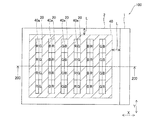
図9〜図11は、それぞれ、上記した本発明の液晶表示装置100、101、102、103および104を用いた電子機器の第1の例〜第3の例を説明するための図である。図9〜図11を参照して、本発明の第1〜第5実施形態による液晶表示装置100〜104を用いた電子機器について説明する。
Claims (8)
- 表面上にトランジスタ素子が形成された素子基板と、
前記トランジスタ素子を挟むように、前記素子基板と対向するように配置された対向基板と、
前記対向基板の前記トランジスタ素子側とは反対側の表面上に直接形成された視差バリアパターンと、
前記対向基板の視差バリアパターン側とは反対側の表面上に形成されたカラーフィルターとを備え、
前記対向基板の厚みが、前記素子基板の厚みよりも小さく、
前記視差バリアパターンは、前記素子基板と前記対向基板とが張り合わされた後に形成されたものであって、前記対向基板の前記トランジスタ素子側とは反対側の表面上に直接形成された複数の開口部を有する金属層からなるとともに、前記素子基板側と導通している、表示装置。 - 前記視差バリアパターンは、前記対向基板の前記トランジスタ素子側とは反対側の表面上に接着材層を介さずに直接接触するように形成されている、請求項1に記載の表示装置。
- 前記視差バリアパターンの端部は、前記対向基板の端部よりも内側に形成されている、請求項1または2に記載の表示装置。
- 前記視差バリアパターンの前記トランジスタ素子側とは反対側の表面上に形成された保護膜と、
前記保護膜の前記トランジスタ素子側とは反対側の表面上に形成された偏光板とをさらに備える、請求項1〜3のいずれか1項に記載の表示装置。 - 前記視差バリアパターンの前記トランジスタ素子側とは反対側の表面上に形成された偏光板と、
前記偏光板の前記トランジスタ素子側とは反対側の表面上に形成された保護膜とをさらに備える、請求項1〜4のいずれか1項に記載の表示装置。 - 前記視差バリアパターンの一部分は、露出するように構成されており、
前記視差バリアパターンの露出した部分と、前記素子基板側とを導通させるための導通部材をさらに備える、請求項1〜5のいずれか1項に記載の表示装置。 - 画像を分離することにより2つの異なる画像を表示させる2画面表示用の表示装置である、請求項1〜6のいずれか1項に記載の表示装置。
- 請求項1〜7のいずれか1項に記載の表示装置を備える電子機器。
Priority Applications (3)
| Application Number | Priority Date | Filing Date | Title |
|---|---|---|---|
| JP2010030983A JP5567855B2 (ja) | 2010-02-16 | 2010-02-16 | 表示装置および電子機器 |
| CN201110034309.9A CN102162947B (zh) | 2010-02-16 | 2011-02-01 | 显示装置及电子设备 |
| US13/023,869 US8817197B2 (en) | 2010-02-16 | 2011-02-09 | Display device and electronic apparatus |
Applications Claiming Priority (1)
| Application Number | Priority Date | Filing Date | Title |
|---|---|---|---|
| JP2010030983A JP5567855B2 (ja) | 2010-02-16 | 2010-02-16 | 表示装置および電子機器 |
Publications (2)
| Publication Number | Publication Date |
|---|---|
| JP2011169942A JP2011169942A (ja) | 2011-09-01 |
| JP5567855B2 true JP5567855B2 (ja) | 2014-08-06 |
Family
ID=44369425
Family Applications (1)
| Application Number | Title | Priority Date | Filing Date |
|---|---|---|---|
| JP2010030983A Active JP5567855B2 (ja) | 2010-02-16 | 2010-02-16 | 表示装置および電子機器 |
Country Status (3)
| Country | Link |
|---|---|
| US (1) | US8817197B2 (ja) |
| JP (1) | JP5567855B2 (ja) |
| CN (1) | CN102162947B (ja) |
Families Citing this family (17)
| Publication number | Priority date | Publication date | Assignee | Title |
|---|---|---|---|---|
| JP5730091B2 (ja) * | 2011-03-25 | 2015-06-03 | 株式会社ジャパンディスプレイ | 表示パネル、表示装置および電子機器 |
| JP5604359B2 (ja) * | 2011-04-12 | 2014-10-08 | 株式会社ジャパンディスプレイ | 表示パネル、表示装置および電子機器 |
| JP2013140276A (ja) | 2012-01-05 | 2013-07-18 | Sony Corp | 表示装置 |
| JP5962229B2 (ja) * | 2012-06-05 | 2016-08-03 | 三菱電機株式会社 | 表示装置 |
| CN102722044B (zh) * | 2012-06-07 | 2015-05-20 | 深圳市华星光电技术有限公司 | 立体显示系统 |
| JP5933362B2 (ja) * | 2012-06-19 | 2016-06-08 | 三菱電機株式会社 | 液晶表示装置およびその製造方法 |
| US9851593B2 (en) * | 2012-09-11 | 2017-12-26 | Apple Inc. | LCD frame assembly |
| CN102854655B (zh) * | 2012-09-25 | 2015-07-22 | 深圳市华星光电技术有限公司 | 一种液晶面板及其制作方法 |
| WO2014185894A1 (en) * | 2013-05-14 | 2014-11-20 | Apple Inc. | Displays with color filter material in border regions |
| CN103744248A (zh) * | 2013-11-28 | 2014-04-23 | 深圳市华星光电技术有限公司 | 显示装置及液晶盒透镜面板 |
| US20150146115A1 (en) * | 2013-11-28 | 2015-05-28 | Shenzhen China Star Optoelectronics Technology Co. Ltd. | Dispaly device and liquid crystal prism cell panel |
| US10162214B2 (en) | 2014-05-21 | 2018-12-25 | Sharp Kabushiki Kaisha | Liquid crystal display device, optical control member, and base material for manufacturing optical control member |
| CN104460100B (zh) * | 2014-11-26 | 2018-03-27 | 京东方科技集团股份有限公司 | 显示基板和显示面板及其制作方法、显示装置 |
| CN104460016B (zh) * | 2014-12-23 | 2017-08-08 | 上海天马微电子有限公司 | 3d显示面板及3d液晶显示装置 |
| CN105527742A (zh) * | 2016-02-25 | 2016-04-27 | 京东方科技集团股份有限公司 | 一种3d显示装置及其驱动方法 |
| WO2017195323A1 (ja) * | 2016-05-12 | 2017-11-16 | シャープ株式会社 | 液晶表示装置 |
| GB2571921A (en) * | 2018-03-05 | 2019-09-18 | Flexenable Ltd | Displays |
Family Cites Families (17)
| Publication number | Priority date | Publication date | Assignee | Title |
|---|---|---|---|---|
| JPH08106070A (ja) * | 1994-08-08 | 1996-04-23 | Sanyo Electric Co Ltd | 光シャッター及び3次元画像表示装置 |
| JP3598948B2 (ja) * | 1996-03-14 | 2004-12-08 | セイコーエプソン株式会社 | 液晶装置及びそれを用いた電子機器 |
| US7365908B2 (en) * | 2001-11-08 | 2008-04-29 | Eugene Dolgoff | Tiling of panels for multiple-image displays |
| AU2003281711A1 (en) * | 2002-07-29 | 2004-02-16 | Sharp Kabushiki Kaisha | Substrate with parallax barrier layer, method for producing substrate with parallax barrier layer, and three-dimensional display |
| GB2396070A (en) | 2002-12-07 | 2004-06-09 | Sharp Kk | Multiple view display |
| CN100498924C (zh) * | 2004-11-02 | 2009-06-10 | 富士通天株式会社 | 显示控制装置和显示装置 |
| US7697105B2 (en) * | 2005-07-11 | 2010-04-13 | Sharp Kabushiki Kaisha | Display device including a parallax barrier |
| US7626674B2 (en) * | 2005-07-11 | 2009-12-01 | Sharp Kabushiki Kaisha | Display device having particular parallax barrier |
| JP2007222214A (ja) * | 2006-02-21 | 2007-09-06 | Aruze Corp | ゲーム装置 |
| JP2008008934A (ja) * | 2006-06-27 | 2008-01-17 | Toshiba Matsushita Display Technology Co Ltd | 表示素子およびその製造方法 |
| JP2008064918A (ja) * | 2006-09-06 | 2008-03-21 | Seiko Epson Corp | 電気光学装置、液晶装置及び電子機器 |
| US20080158500A1 (en) * | 2006-12-27 | 2008-07-03 | Yasushi Kawata | Display Device and Method for Manufacturing the Same |
| JP2008164702A (ja) * | 2006-12-27 | 2008-07-17 | Toshiba Matsushita Display Technology Co Ltd | 表示素子およびその製造方法 |
| JP2008164703A (ja) * | 2006-12-27 | 2008-07-17 | Toshiba Matsushita Display Technology Co Ltd | 表示素子およびその製造方法 |
| JP2008224930A (ja) * | 2007-03-12 | 2008-09-25 | Seiko Epson Corp | 表示装置とその製造方法、及び電子機器 |
| US20100182530A1 (en) * | 2007-09-28 | 2010-07-22 | Sharp Kabushiki Kaisha | Display cell |
| CN101821704B (zh) * | 2007-11-29 | 2013-03-27 | 夏普株式会社 | 显示装置 |
-
2010
- 2010-02-16 JP JP2010030983A patent/JP5567855B2/ja active Active
-
2011
- 2011-02-01 CN CN201110034309.9A patent/CN102162947B/zh active Active
- 2011-02-09 US US13/023,869 patent/US8817197B2/en active Active
Also Published As
| Publication number | Publication date |
|---|---|
| JP2011169942A (ja) | 2011-09-01 |
| US8817197B2 (en) | 2014-08-26 |
| CN102162947A (zh) | 2011-08-24 |
| US20110199549A1 (en) | 2011-08-18 |
| CN102162947B (zh) | 2015-08-26 |
Similar Documents
| Publication | Publication Date | Title |
|---|---|---|
| JP5567855B2 (ja) | 表示装置および電子機器 | |
| TWI629623B (zh) | Display device | |
| US9666648B2 (en) | Organic electroluminescent display device having an input function | |
| JP5717326B2 (ja) | 液晶装置、電子機器、液晶装置の製造方法 | |
| WO2018216545A1 (ja) | 表示デバイス | |
| US10001676B2 (en) | Display device | |
| CN106886109B (zh) | 显示装置 | |
| WO2017022614A1 (ja) | 表示装置 | |
| US11003029B2 (en) | Display device | |
| JP2014026199A (ja) | 液晶表示装置 | |
| WO2018152880A1 (zh) | 一种触摸显示屏及其制造方法 | |
| JP2018031977A (ja) | 表示装置 | |
| JP2010210982A (ja) | 液晶表示装置 | |
| JP5604359B2 (ja) | 表示パネル、表示装置および電子機器 | |
| JP2017111327A (ja) | 液晶表示装置 | |
| JP2010204406A (ja) | 液晶表示装置 | |
| JP2012203348A (ja) | 液晶表示装置 | |
| JP2013190715A (ja) | 表示装置、製造方法、電子機器 | |
| JP2012073669A (ja) | タッチパネル及び画像表示装置 | |
| JP2014106322A (ja) | 液晶表示装置 | |
| JP2005062760A (ja) | 電気光学装置および電子機器 | |
| JP5939755B2 (ja) | 液晶表示装置 | |
| WO2020026780A1 (ja) | 表示装置 | |
| JP5392702B2 (ja) | 液晶表示装置および電子機器 | |
| JP2018091914A (ja) | 表示装置 |
Legal Events
| Date | Code | Title | Description |
|---|---|---|---|
| A711 | Notification of change in applicant |
Free format text: JAPANESE INTERMEDIATE CODE: A711 Effective date: 20120330 |
|
| A621 | Written request for application examination |
Free format text: JAPANESE INTERMEDIATE CODE: A621 Effective date: 20130104 |
|
| RD03 | Notification of appointment of power of attorney |
Free format text: JAPANESE INTERMEDIATE CODE: A7423 Effective date: 20130328 |
|
| A977 | Report on retrieval |
Free format text: JAPANESE INTERMEDIATE CODE: A971007 Effective date: 20130522 |
|
| A131 | Notification of reasons for refusal |
Free format text: JAPANESE INTERMEDIATE CODE: A131 Effective date: 20130528 |
|
| A521 | Request for written amendment filed |
Free format text: JAPANESE INTERMEDIATE CODE: A523 Effective date: 20130725 |
|
| A711 | Notification of change in applicant |
Free format text: JAPANESE INTERMEDIATE CODE: A712 Effective date: 20130725 |
|
| A131 | Notification of reasons for refusal |
Free format text: JAPANESE INTERMEDIATE CODE: A131 Effective date: 20131029 |
|
| TRDD | Decision of grant or rejection written | ||
| A01 | Written decision to grant a patent or to grant a registration (utility model) |
Free format text: JAPANESE INTERMEDIATE CODE: A01 Effective date: 20140610 |
|
| A61 | First payment of annual fees (during grant procedure) |
Free format text: JAPANESE INTERMEDIATE CODE: A61 Effective date: 20140620 |
|
| R150 | Certificate of patent or registration of utility model |
Ref document number: 5567855 Country of ref document: JP Free format text: JAPANESE INTERMEDIATE CODE: R150 |
|
| R250 | Receipt of annual fees |
Free format text: JAPANESE INTERMEDIATE CODE: R250 |
|
| R250 | Receipt of annual fees |
Free format text: JAPANESE INTERMEDIATE CODE: R250 |
|
| R250 | Receipt of annual fees |
Free format text: JAPANESE INTERMEDIATE CODE: R250 |
|
| R250 | Receipt of annual fees |
Free format text: JAPANESE INTERMEDIATE CODE: R250 |
|
| R250 | Receipt of annual fees |
Free format text: JAPANESE INTERMEDIATE CODE: R250 |
|
| R250 | Receipt of annual fees |
Free format text: JAPANESE INTERMEDIATE CODE: R250 |
|
| R250 | Receipt of annual fees |
Free format text: JAPANESE INTERMEDIATE CODE: R250 |