JP5559547B2 - 半導体デバイスを作る方法 - Google Patents
半導体デバイスを作る方法 Download PDFInfo
- Publication number
- JP5559547B2 JP5559547B2 JP2009551780A JP2009551780A JP5559547B2 JP 5559547 B2 JP5559547 B2 JP 5559547B2 JP 2009551780 A JP2009551780 A JP 2009551780A JP 2009551780 A JP2009551780 A JP 2009551780A JP 5559547 B2 JP5559547 B2 JP 5559547B2
- Authority
- JP
- Japan
- Prior art keywords
- semiconductor device
- gate structure
- doped region
- semiconductor
- channel
- Prior art date
- Legal status (The legal status is an assumption and is not a legal conclusion. Google has not performed a legal analysis and makes no representation as to the accuracy of the status listed.)
- Expired - Fee Related
Links
- 239000004065 semiconductor Substances 0.000 title claims description 81
- 125000006850 spacer group Chemical group 0.000 claims description 31
- 239000000463 material Substances 0.000 claims description 27
- 238000000034 method Methods 0.000 claims description 19
- 239000007943 implant Substances 0.000 claims description 18
- 239000000758 substrate Substances 0.000 claims description 10
- 229910000577 Silicon-germanium Inorganic materials 0.000 claims description 9
- 238000000137 annealing Methods 0.000 claims description 5
- ZOXJGFHDIHLPTG-UHFFFAOYSA-N Boron Chemical compound [B] ZOXJGFHDIHLPTG-UHFFFAOYSA-N 0.000 claims description 4
- 229910052785 arsenic Inorganic materials 0.000 claims description 4
- RQNWIZPPADIBDY-UHFFFAOYSA-N arsenic atom Chemical compound [As] RQNWIZPPADIBDY-UHFFFAOYSA-N 0.000 claims description 4
- 229910052796 boron Inorganic materials 0.000 claims description 4
- 238000005530 etching Methods 0.000 claims description 4
- 229910052698 phosphorus Inorganic materials 0.000 claims description 4
- 229910021332 silicide Inorganic materials 0.000 claims description 4
- FVBUAEGBCNSCDD-UHFFFAOYSA-N silicide(4-) Chemical compound [Si-4] FVBUAEGBCNSCDD-UHFFFAOYSA-N 0.000 claims description 4
- OAICVXFJPJFONN-UHFFFAOYSA-N Phosphorus Chemical compound [P] OAICVXFJPJFONN-UHFFFAOYSA-N 0.000 claims description 3
- LEVVHYCKPQWKOP-UHFFFAOYSA-N [Si].[Ge] Chemical compound [Si].[Ge] LEVVHYCKPQWKOP-UHFFFAOYSA-N 0.000 claims description 3
- 239000011574 phosphorus Substances 0.000 claims description 3
- HBMJWWWQQXIZIP-UHFFFAOYSA-N silicon carbide Chemical compound [Si+]#[C-] HBMJWWWQQXIZIP-UHFFFAOYSA-N 0.000 claims description 3
- 229910052787 antimony Inorganic materials 0.000 claims description 2
- WATWJIUSRGPENY-UHFFFAOYSA-N antimony atom Chemical compound [Sb] WATWJIUSRGPENY-UHFFFAOYSA-N 0.000 claims description 2
- 229910052738 indium Inorganic materials 0.000 claims description 2
- APFVFJFRJDLVQX-UHFFFAOYSA-N indium atom Chemical compound [In] APFVFJFRJDLVQX-UHFFFAOYSA-N 0.000 claims description 2
- 229910010271 silicon carbide Inorganic materials 0.000 claims description 2
- 238000004519 manufacturing process Methods 0.000 claims 1
- 239000010410 layer Substances 0.000 description 37
- 230000008569 process Effects 0.000 description 9
- XUIMIQQOPSSXEZ-UHFFFAOYSA-N Silicon Chemical compound [Si] XUIMIQQOPSSXEZ-UHFFFAOYSA-N 0.000 description 7
- 238000004140 cleaning Methods 0.000 description 7
- 229910052710 silicon Inorganic materials 0.000 description 7
- 239000010703 silicon Substances 0.000 description 7
- 230000015572 biosynthetic process Effects 0.000 description 5
- 238000011065 in-situ storage Methods 0.000 description 4
- 239000000126 substance Substances 0.000 description 4
- 229920002120 photoresistant polymer Polymers 0.000 description 3
- OKTJSMMVPCPJKN-UHFFFAOYSA-N Carbon Chemical compound [C] OKTJSMMVPCPJKN-UHFFFAOYSA-N 0.000 description 2
- 230000008901 benefit Effects 0.000 description 2
- 229910052799 carbon Inorganic materials 0.000 description 2
- 239000002019 doping agent Substances 0.000 description 2
- 229910052732 germanium Inorganic materials 0.000 description 2
- GNPVGFCGXDBREM-UHFFFAOYSA-N germanium atom Chemical compound [Ge] GNPVGFCGXDBREM-UHFFFAOYSA-N 0.000 description 2
- 238000002513 implantation Methods 0.000 description 2
- 229910052751 metal Inorganic materials 0.000 description 2
- 239000002184 metal Substances 0.000 description 2
- 238000012986 modification Methods 0.000 description 2
- 230000004048 modification Effects 0.000 description 2
- 230000003071 parasitic effect Effects 0.000 description 2
- 239000002356 single layer Substances 0.000 description 2
- UFHFLCQGNIYNRP-UHFFFAOYSA-N Hydrogen Chemical compound [H][H] UFHFLCQGNIYNRP-UHFFFAOYSA-N 0.000 description 1
- 230000003213 activating effect Effects 0.000 description 1
- 230000004888 barrier function Effects 0.000 description 1
- 239000000969 carrier Substances 0.000 description 1
- 230000001364 causal effect Effects 0.000 description 1
- 230000006835 compression Effects 0.000 description 1
- 238000007906 compression Methods 0.000 description 1
- 238000009792 diffusion process Methods 0.000 description 1
- 230000000694 effects Effects 0.000 description 1
- 238000005421 electrostatic potential Methods 0.000 description 1
- 230000014509 gene expression Effects 0.000 description 1
- BHEPBYXIRTUNPN-UHFFFAOYSA-N hydridophosphorus(.) (triplet) Chemical compound [PH] BHEPBYXIRTUNPN-UHFFFAOYSA-N 0.000 description 1
- 230000006872 improvement Effects 0.000 description 1
- 239000011229 interlayer Substances 0.000 description 1
- 150000004767 nitrides Chemical class 0.000 description 1
- 229910052757 nitrogen Inorganic materials 0.000 description 1
- 238000000059 patterning Methods 0.000 description 1
- 229910021420 polycrystalline silicon Inorganic materials 0.000 description 1
- 229920005591 polysilicon Polymers 0.000 description 1
- 238000002360 preparation method Methods 0.000 description 1
- 230000009467 reduction Effects 0.000 description 1
- 230000002040 relaxant effect Effects 0.000 description 1
Images


Classifications
-
- H—ELECTRICITY
- H01—ELECTRIC ELEMENTS
- H01L—SEMICONDUCTOR DEVICES NOT COVERED BY CLASS H10
- H01L21/00—Processes or apparatus adapted for the manufacture or treatment of semiconductor or solid state devices or of parts thereof
- H01L21/02—Manufacture or treatment of semiconductor devices or of parts thereof
- H01L21/04—Manufacture or treatment of semiconductor devices or of parts thereof the devices having at least one potential-jump barrier or surface barrier, e.g. PN junction, depletion layer or carrier concentration layer
- H01L21/18—Manufacture or treatment of semiconductor devices or of parts thereof the devices having at least one potential-jump barrier or surface barrier, e.g. PN junction, depletion layer or carrier concentration layer the devices having semiconductor bodies comprising elements of Group IV of the Periodic System or AIIIBV compounds with or without impurities, e.g. doping materials
- H01L21/26—Bombardment with radiation
- H01L21/263—Bombardment with radiation with high-energy radiation
- H01L21/265—Bombardment with radiation with high-energy radiation producing ion implantation
-
- H—ELECTRICITY
- H01—ELECTRIC ELEMENTS
- H01L—SEMICONDUCTOR DEVICES NOT COVERED BY CLASS H10
- H01L29/00—Semiconductor devices adapted for rectifying, amplifying, oscillating or switching, or capacitors or resistors with at least one potential-jump barrier or surface barrier, e.g. PN junction depletion layer or carrier concentration layer; Details of semiconductor bodies or of electrodes thereof ; Multistep manufacturing processes therefor
- H01L29/66—Types of semiconductor device ; Multistep manufacturing processes therefor
- H01L29/66007—Multistep manufacturing processes
- H01L29/66075—Multistep manufacturing processes of devices having semiconductor bodies comprising group 14 or group 13/15 materials
- H01L29/66227—Multistep manufacturing processes of devices having semiconductor bodies comprising group 14 or group 13/15 materials the devices being controllable only by the electric current supplied or the electric potential applied, to an electrode which does not carry the current to be rectified, amplified or switched, e.g. three-terminal devices
- H01L29/66409—Unipolar field-effect transistors
- H01L29/66477—Unipolar field-effect transistors with an insulated gate, i.e. MISFET
- H01L29/66568—Lateral single gate silicon transistors
- H01L29/66613—Lateral single gate silicon transistors with a gate recessing step, e.g. using local oxidation
- H01L29/66628—Lateral single gate silicon transistors with a gate recessing step, e.g. using local oxidation recessing the gate by forming single crystalline semiconductor material at the source or drain location
-
- H—ELECTRICITY
- H01—ELECTRIC ELEMENTS
- H01L—SEMICONDUCTOR DEVICES NOT COVERED BY CLASS H10
- H01L21/00—Processes or apparatus adapted for the manufacture or treatment of semiconductor or solid state devices or of parts thereof
- H01L21/02—Manufacture or treatment of semiconductor devices or of parts thereof
- H01L21/04—Manufacture or treatment of semiconductor devices or of parts thereof the devices having at least one potential-jump barrier or surface barrier, e.g. PN junction, depletion layer or carrier concentration layer
- H01L21/18—Manufacture or treatment of semiconductor devices or of parts thereof the devices having at least one potential-jump barrier or surface barrier, e.g. PN junction, depletion layer or carrier concentration layer the devices having semiconductor bodies comprising elements of Group IV of the Periodic System or AIIIBV compounds with or without impurities, e.g. doping materials
- H01L21/26—Bombardment with radiation
- H01L21/263—Bombardment with radiation with high-energy radiation
- H01L21/265—Bombardment with radiation with high-energy radiation producing ion implantation
- H01L21/26586—Bombardment with radiation with high-energy radiation producing ion implantation characterised by the angle between the ion beam and the crystal planes or the main crystal surface
-
- H—ELECTRICITY
- H01—ELECTRIC ELEMENTS
- H01L—SEMICONDUCTOR DEVICES NOT COVERED BY CLASS H10
- H01L29/00—Semiconductor devices adapted for rectifying, amplifying, oscillating or switching, or capacitors or resistors with at least one potential-jump barrier or surface barrier, e.g. PN junction depletion layer or carrier concentration layer; Details of semiconductor bodies or of electrodes thereof ; Multistep manufacturing processes therefor
- H01L29/66—Types of semiconductor device ; Multistep manufacturing processes therefor
- H01L29/66007—Multistep manufacturing processes
- H01L29/66075—Multistep manufacturing processes of devices having semiconductor bodies comprising group 14 or group 13/15 materials
- H01L29/66227—Multistep manufacturing processes of devices having semiconductor bodies comprising group 14 or group 13/15 materials the devices being controllable only by the electric current supplied or the electric potential applied, to an electrode which does not carry the current to be rectified, amplified or switched, e.g. three-terminal devices
- H01L29/66409—Unipolar field-effect transistors
- H01L29/66477—Unipolar field-effect transistors with an insulated gate, i.e. MISFET
- H01L29/66568—Lateral single gate silicon transistors
- H01L29/66613—Lateral single gate silicon transistors with a gate recessing step, e.g. using local oxidation
- H01L29/66621—Lateral single gate silicon transistors with a gate recessing step, e.g. using local oxidation using etching to form a recess at the gate location
-
- H—ELECTRICITY
- H01—ELECTRIC ELEMENTS
- H01L—SEMICONDUCTOR DEVICES NOT COVERED BY CLASS H10
- H01L29/00—Semiconductor devices adapted for rectifying, amplifying, oscillating or switching, or capacitors or resistors with at least one potential-jump barrier or surface barrier, e.g. PN junction depletion layer or carrier concentration layer; Details of semiconductor bodies or of electrodes thereof ; Multistep manufacturing processes therefor
- H01L29/66—Types of semiconductor device ; Multistep manufacturing processes therefor
- H01L29/66007—Multistep manufacturing processes
- H01L29/66075—Multistep manufacturing processes of devices having semiconductor bodies comprising group 14 or group 13/15 materials
- H01L29/66227—Multistep manufacturing processes of devices having semiconductor bodies comprising group 14 or group 13/15 materials the devices being controllable only by the electric current supplied or the electric potential applied, to an electrode which does not carry the current to be rectified, amplified or switched, e.g. three-terminal devices
- H01L29/66409—Unipolar field-effect transistors
- H01L29/66477—Unipolar field-effect transistors with an insulated gate, i.e. MISFET
- H01L29/66568—Lateral single gate silicon transistors
- H01L29/66659—Lateral single gate silicon transistors with asymmetry in the channel direction, e.g. lateral high-voltage MISFETs with drain offset region, extended drain MISFETs
-
- H—ELECTRICITY
- H01—ELECTRIC ELEMENTS
- H01L—SEMICONDUCTOR DEVICES NOT COVERED BY CLASS H10
- H01L29/00—Semiconductor devices adapted for rectifying, amplifying, oscillating or switching, or capacitors or resistors with at least one potential-jump barrier or surface barrier, e.g. PN junction depletion layer or carrier concentration layer; Details of semiconductor bodies or of electrodes thereof ; Multistep manufacturing processes therefor
- H01L29/66—Types of semiconductor device ; Multistep manufacturing processes therefor
- H01L29/68—Types of semiconductor device ; Multistep manufacturing processes therefor controllable by only the electric current supplied, or only the electric potential applied, to an electrode which does not carry the current to be rectified, amplified or switched
- H01L29/76—Unipolar devices, e.g. field effect transistors
- H01L29/772—Field effect transistors
- H01L29/78—Field effect transistors with field effect produced by an insulated gate
- H01L29/7833—Field effect transistors with field effect produced by an insulated gate with lightly doped drain or source extension, e.g. LDD MOSFET's; DDD MOSFET's
- H01L29/7835—Field effect transistors with field effect produced by an insulated gate with lightly doped drain or source extension, e.g. LDD MOSFET's; DDD MOSFET's with asymmetrical source and drain regions, e.g. lateral high-voltage MISFETs with drain offset region, extended drain MISFETs
-
- H—ELECTRICITY
- H01—ELECTRIC ELEMENTS
- H01L—SEMICONDUCTOR DEVICES NOT COVERED BY CLASS H10
- H01L29/00—Semiconductor devices adapted for rectifying, amplifying, oscillating or switching, or capacitors or resistors with at least one potential-jump barrier or surface barrier, e.g. PN junction depletion layer or carrier concentration layer; Details of semiconductor bodies or of electrodes thereof ; Multistep manufacturing processes therefor
- H01L29/66—Types of semiconductor device ; Multistep manufacturing processes therefor
- H01L29/68—Types of semiconductor device ; Multistep manufacturing processes therefor controllable by only the electric current supplied, or only the electric potential applied, to an electrode which does not carry the current to be rectified, amplified or switched
- H01L29/76—Unipolar devices, e.g. field effect transistors
- H01L29/772—Field effect transistors
- H01L29/78—Field effect transistors with field effect produced by an insulated gate
- H01L29/7842—Field effect transistors with field effect produced by an insulated gate means for exerting mechanical stress on the crystal lattice of the channel region, e.g. using a flexible substrate
- H01L29/7848—Field effect transistors with field effect produced by an insulated gate means for exerting mechanical stress on the crystal lattice of the channel region, e.g. using a flexible substrate the means being located in the source/drain region, e.g. SiGe source and drain
-
- H—ELECTRICITY
- H01—ELECTRIC ELEMENTS
- H01L—SEMICONDUCTOR DEVICES NOT COVERED BY CLASS H10
- H01L29/00—Semiconductor devices adapted for rectifying, amplifying, oscillating or switching, or capacitors or resistors with at least one potential-jump barrier or surface barrier, e.g. PN junction depletion layer or carrier concentration layer; Details of semiconductor bodies or of electrodes thereof ; Multistep manufacturing processes therefor
- H01L29/66—Types of semiconductor device ; Multistep manufacturing processes therefor
- H01L29/66007—Multistep manufacturing processes
- H01L29/66075—Multistep manufacturing processes of devices having semiconductor bodies comprising group 14 or group 13/15 materials
- H01L29/66227—Multistep manufacturing processes of devices having semiconductor bodies comprising group 14 or group 13/15 materials the devices being controllable only by the electric current supplied or the electric potential applied, to an electrode which does not carry the current to be rectified, amplified or switched, e.g. three-terminal devices
- H01L29/66409—Unipolar field-effect transistors
- H01L29/66477—Unipolar field-effect transistors with an insulated gate, i.e. MISFET
- H01L29/665—Unipolar field-effect transistors with an insulated gate, i.e. MISFET using self aligned silicidation, i.e. salicide
-
- H—ELECTRICITY
- H01—ELECTRIC ELEMENTS
- H01L—SEMICONDUCTOR DEVICES NOT COVERED BY CLASS H10
- H01L29/00—Semiconductor devices adapted for rectifying, amplifying, oscillating or switching, or capacitors or resistors with at least one potential-jump barrier or surface barrier, e.g. PN junction depletion layer or carrier concentration layer; Details of semiconductor bodies or of electrodes thereof ; Multistep manufacturing processes therefor
- H01L29/66—Types of semiconductor device ; Multistep manufacturing processes therefor
- H01L29/66007—Multistep manufacturing processes
- H01L29/66075—Multistep manufacturing processes of devices having semiconductor bodies comprising group 14 or group 13/15 materials
- H01L29/66227—Multistep manufacturing processes of devices having semiconductor bodies comprising group 14 or group 13/15 materials the devices being controllable only by the electric current supplied or the electric potential applied, to an electrode which does not carry the current to be rectified, amplified or switched, e.g. three-terminal devices
- H01L29/66409—Unipolar field-effect transistors
- H01L29/66477—Unipolar field-effect transistors with an insulated gate, i.e. MISFET
- H01L29/6656—Unipolar field-effect transistors with an insulated gate, i.e. MISFET using multiple spacer layers, e.g. multiple sidewall spacers
-
- H—ELECTRICITY
- H01—ELECTRIC ELEMENTS
- H01L—SEMICONDUCTOR DEVICES NOT COVERED BY CLASS H10
- H01L29/00—Semiconductor devices adapted for rectifying, amplifying, oscillating or switching, or capacitors or resistors with at least one potential-jump barrier or surface barrier, e.g. PN junction depletion layer or carrier concentration layer; Details of semiconductor bodies or of electrodes thereof ; Multistep manufacturing processes therefor
- H01L29/66—Types of semiconductor device ; Multistep manufacturing processes therefor
- H01L29/66007—Multistep manufacturing processes
- H01L29/66075—Multistep manufacturing processes of devices having semiconductor bodies comprising group 14 or group 13/15 materials
- H01L29/66227—Multistep manufacturing processes of devices having semiconductor bodies comprising group 14 or group 13/15 materials the devices being controllable only by the electric current supplied or the electric potential applied, to an electrode which does not carry the current to be rectified, amplified or switched, e.g. three-terminal devices
- H01L29/66409—Unipolar field-effect transistors
- H01L29/66477—Unipolar field-effect transistors with an insulated gate, i.e. MISFET
- H01L29/66568—Lateral single gate silicon transistors
- H01L29/66636—Lateral single gate silicon transistors with source or drain recessed by etching or first recessed by etching and then refilled
-
- H—ELECTRICITY
- H01—ELECTRIC ELEMENTS
- H01L—SEMICONDUCTOR DEVICES NOT COVERED BY CLASS H10
- H01L29/00—Semiconductor devices adapted for rectifying, amplifying, oscillating or switching, or capacitors or resistors with at least one potential-jump barrier or surface barrier, e.g. PN junction depletion layer or carrier concentration layer; Details of semiconductor bodies or of electrodes thereof ; Multistep manufacturing processes therefor
- H01L29/66—Types of semiconductor device ; Multistep manufacturing processes therefor
- H01L29/66007—Multistep manufacturing processes
- H01L29/66075—Multistep manufacturing processes of devices having semiconductor bodies comprising group 14 or group 13/15 materials
- H01L29/66227—Multistep manufacturing processes of devices having semiconductor bodies comprising group 14 or group 13/15 materials the devices being controllable only by the electric current supplied or the electric potential applied, to an electrode which does not carry the current to be rectified, amplified or switched, e.g. three-terminal devices
- H01L29/66409—Unipolar field-effect transistors
- H01L29/66477—Unipolar field-effect transistors with an insulated gate, i.e. MISFET
- H01L29/66742—Thin film unipolar transistors
- H01L29/66772—Monocristalline silicon transistors on insulating substrates, e.g. quartz substrates
Description
Claims (10)
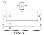
- 半導体デバイスを作る方法であって、
基板の上に横たわるゲート構造体を形成するステップと、
前記ゲート構造体に隣接する側壁スペーサを形成するステップと、
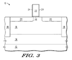
前記半導体デバイスのドレイン側に第2のドープ領域とソース側に第1のドープ領域とを形成するために、前記半導体デバイスのドレイン側にマスクとして作用するゲート構造体を使用して前記半導体デバイスのソース側の方向に、角度をつけたインプラントを実施するステップであって、前記第1のドープ領域が前記ゲート構造体の一部の下に延び、前記第2のドープ領域が前記ゲート構造体及び前記側壁スペーサから間隔が隔てられることを特徴とするステップと、
前記半導体デバイスをアニーリングするステップと、
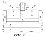
前記ゲート構造体および前記側壁スペーサをマスクとして使用することにより、前記ゲート構造体の下の第1のドープ領域の一部を残すように基板をエッチングすることにより、基板の側壁スペーサの対向する端に隣接してレセスを形成するステップと、
前記レセスに第2の型の半導体材料をエピタキシャル成長させるステップと、
を有し、
前記第2の型の半導体材料が、前記第1の型の半導体材料の格子定数とは異なる本来の格子定数を備え、半導体デバイスのチャネル領域に応力を生成することを特徴とする、方法。 - ドーピング材料を使用して、前記第2の型の半導体材料にドーピングを実行するステップを更に有することを特徴とする請求項1に記載の方法。
- 前記角度をつけたインプラントが、垂直軸線に対して5度ないし30度の角度で実行されることを特徴とする請求項1又は2に記載の方法。
- 前記半導体デバイスが、Pチャネルデバイスであり、前記ドーピング材料が、ホウ素、BF2およびインジウムからなるグループの一つからなり、前記第2の型の半導体材料がシリコンゲルマニウムであることを特徴とする請求項1乃至3のいずれか1項に記載の方法。
- 半導体デバイスがNチャネルデバイスであり、ドーピング材料が、燐、ヒ素、および、アンチモンからなるグループの一つからなり、第2の型の半導体材料が炭化珪素であることを特徴とする請求項1乃至3のいずれか1項に記載の方法。
- 半導体デバイスがPチャネルデバイスであり、ドーピング材料がホウ素であることを特徴とする請求項1乃至4のいずれか1項に記載の方法。
- 半導体デバイスがNチャネルデバイスであり、ドーピング材料が燐およびヒ素からなるグループの一つからなることを特徴とする請求項1乃至3又は5のいずれか1項に記載の方法。
- レセスに第2の型の半導体材料をエピタキシャル成長させた後に、前記アニーリングするステップが実行されることを特徴とする請求項1乃至7のいずれか1項に記載の方法。
- 前記側壁スペーサの幅が40オングストローム乃至100オングストロームの範囲であることを特徴とする請求項1乃至8のいずれか1項に記載の方法。
- 前記第2の型の半導体材料と前記ゲート構造体の上にシリサイド層を形成するステップと、を更に有することを特徴とする請求項1乃至9のいずれか1項に記載の方法。
Applications Claiming Priority (3)
| Application Number | Priority Date | Filing Date | Title |
|---|---|---|---|
| US11/680,181 US7572706B2 (en) | 2007-02-28 | 2007-02-28 | Source/drain stressor and method therefor |
| US11/680,181 | 2007-02-28 | ||
| PCT/US2008/053563 WO2008106304A1 (en) | 2007-02-28 | 2008-02-11 | Source/drain stressor and method therefor |
Publications (3)
| Publication Number | Publication Date |
|---|---|
| JP2010520620A JP2010520620A (ja) | 2010-06-10 |
| JP2010520620A5 JP2010520620A5 (ja) | 2011-03-31 |
| JP5559547B2 true JP5559547B2 (ja) | 2014-07-23 |
Family
ID=39714887
Family Applications (1)
| Application Number | Title | Priority Date | Filing Date |
|---|---|---|---|
| JP2009551780A Expired - Fee Related JP5559547B2 (ja) | 2007-02-28 | 2008-02-11 | 半導体デバイスを作る方法 |
Country Status (7)
| Country | Link |
|---|---|
| US (1) | US7572706B2 (ja) |
| EP (1) | EP2115778A4 (ja) |
| JP (1) | JP5559547B2 (ja) |
| KR (1) | KR101399208B1 (ja) |
| CN (1) | CN101622713B (ja) |
| TW (1) | TWI436431B (ja) |
| WO (1) | WO2008106304A1 (ja) |
Families Citing this family (14)
| Publication number | Priority date | Publication date | Assignee | Title |
|---|---|---|---|---|
| US8080452B2 (en) | 2006-08-01 | 2011-12-20 | Nxp, B.V. | Effecting selectivity of silicon or silicon-germanium deposition on a silicon or silicon-germanium substrate by doping |
| KR100746232B1 (ko) * | 2006-08-25 | 2007-08-03 | 삼성전자주식회사 | 스트레인드 채널을 갖는 모스 트랜지스터 및 그 제조방법 |
| US20080248598A1 (en) * | 2007-04-09 | 2008-10-09 | Rohit Pal | Method and apparatus for determining characteristics of a stressed material using scatterometry |
| US7745847B2 (en) * | 2007-08-09 | 2010-06-29 | United Microelectronics Corp. | Metal oxide semiconductor transistor |
| US20100102393A1 (en) * | 2008-10-29 | 2010-04-29 | Chartered Semiconductor Manufacturing, Ltd. | Metal gate transistors |
| US8124487B2 (en) * | 2008-12-22 | 2012-02-28 | Varian Semiconductor Equipment Associates, Inc. | Method for enhancing tensile stress and source/drain activation using Si:C |
| US20110049582A1 (en) * | 2009-09-03 | 2011-03-03 | International Business Machines Corporation | Asymmetric source and drain stressor regions |
| US8928094B2 (en) * | 2010-09-03 | 2015-01-06 | Taiwan Semiconductor Manufacturing Company, Ltd. | Strained asymmetric source/drain |
| CN102456739A (zh) * | 2010-10-28 | 2012-05-16 | 中国科学院微电子研究所 | 半导体结构及其形成方法 |
| CN102683385B (zh) * | 2012-05-30 | 2014-12-24 | 清华大学 | 半导体结构及其形成方法 |
| KR20140042460A (ko) * | 2012-09-28 | 2014-04-07 | 삼성전자주식회사 | 반도체 소자 |
| KR102137371B1 (ko) * | 2013-10-29 | 2020-07-27 | 삼성전자 주식회사 | 반도체 장치 및 이의 제조 방법 |
| CN106960838B (zh) * | 2016-01-11 | 2019-07-02 | 中芯国际集成电路制造(上海)有限公司 | 静电保护器件及其形成方法 |
| US10032868B2 (en) | 2016-09-09 | 2018-07-24 | Texas Instruments Incorporated | High performance super-beta NPN (SBNPN) |
Family Cites Families (18)
| Publication number | Priority date | Publication date | Assignee | Title |
|---|---|---|---|---|
| JPS6313378A (ja) * | 1986-07-04 | 1988-01-20 | Nippon Telegr & Teleph Corp <Ntt> | 半導体装置およびその製造方法 |
| EP0412701B1 (en) * | 1989-07-31 | 1996-09-25 | Canon Kabushiki Kaisha | Thin film transistor and preparation thereof |
| JPH0423329A (ja) * | 1990-05-14 | 1992-01-27 | Fujitsu Ltd | 半導体装置の製造方法 |
| US5427964A (en) * | 1994-04-04 | 1995-06-27 | Motorola, Inc. | Insulated gate field effect transistor and method for fabricating |
| JPH0992825A (ja) * | 1995-09-26 | 1997-04-04 | Fuji Film Micro Device Kk | 半導体装置およびその製造方法 |
| US6621131B2 (en) | 2001-11-01 | 2003-09-16 | Intel Corporation | Semiconductor transistor having a stressed channel |
| US6833307B1 (en) * | 2002-10-30 | 2004-12-21 | Advanced Micro Devices, Inc. | Method for manufacturing a semiconductor component having an early halo implant |
| JP2004241755A (ja) * | 2003-01-15 | 2004-08-26 | Renesas Technology Corp | 半導体装置 |
| US20040262683A1 (en) * | 2003-06-27 | 2004-12-30 | Bohr Mark T. | PMOS transistor strain optimization with raised junction regions |
| KR100488196B1 (ko) * | 2003-09-29 | 2005-05-09 | 삼성전자주식회사 | 돌출된 드레인을 가지는 트랜지스터 및 이의 제조 방법 |
| US7244654B2 (en) * | 2003-12-31 | 2007-07-17 | Texas Instruments Incorporated | Drive current improvement from recessed SiGe incorporation close to gate |
| JP4837902B2 (ja) * | 2004-06-24 | 2011-12-14 | 富士通セミコンダクター株式会社 | 半導体装置 |
| US7642607B2 (en) * | 2005-08-10 | 2010-01-05 | Taiwan Semiconductor Manufacturing Company, Ltd. | MOS devices with reduced recess on substrate surface |
| US7449753B2 (en) * | 2006-04-10 | 2008-11-11 | Taiwan Semiconductor Manufacturing Company, Ltd. | Write margin improvement for SRAM cells with SiGe stressors |
| US7482211B2 (en) * | 2006-06-22 | 2009-01-27 | Taiwan Semiconductor Manufacturing Company, Ltd. | Junction leakage reduction in SiGe process by implantation |
| US20070298557A1 (en) * | 2006-06-22 | 2007-12-27 | Chun-Feng Nieh | Junction leakage reduction in SiGe process by tilt implantation |
| US8008157B2 (en) * | 2006-10-27 | 2011-08-30 | Taiwan Semiconductor Manufacturing Company, Ltd. | CMOS device with raised source and drain regions |
| CN101641770B (zh) * | 2007-03-28 | 2012-03-07 | 富士通半导体股份有限公司 | 半导体器件及其制造方法 |
-
2007
- 2007-02-28 US US11/680,181 patent/US7572706B2/en not_active Expired - Fee Related
-
2008
- 2008-01-31 TW TW097103705A patent/TWI436431B/zh not_active IP Right Cessation
- 2008-02-11 EP EP08729512A patent/EP2115778A4/en not_active Withdrawn
- 2008-02-11 JP JP2009551780A patent/JP5559547B2/ja not_active Expired - Fee Related
- 2008-02-11 KR KR1020097017872A patent/KR101399208B1/ko not_active IP Right Cessation
- 2008-02-11 CN CN2008800064701A patent/CN101622713B/zh not_active Expired - Fee Related
- 2008-02-11 WO PCT/US2008/053563 patent/WO2008106304A1/en active Application Filing
Also Published As
| Publication number | Publication date |
|---|---|
| CN101622713B (zh) | 2013-10-23 |
| US20080203449A1 (en) | 2008-08-28 |
| EP2115778A4 (en) | 2011-11-02 |
| TWI436431B (zh) | 2014-05-01 |
| KR101399208B1 (ko) | 2014-05-27 |
| EP2115778A1 (en) | 2009-11-11 |
| CN101622713A (zh) | 2010-01-06 |
| JP2010520620A (ja) | 2010-06-10 |
| KR20090125757A (ko) | 2009-12-07 |
| US7572706B2 (en) | 2009-08-11 |
| WO2008106304A1 (en) | 2008-09-04 |
| TW200847299A (en) | 2008-12-01 |
Similar Documents
| Publication | Publication Date | Title |
|---|---|---|
| JP5559547B2 (ja) | 半導体デバイスを作る方法 | |
| JP4439486B2 (ja) | 半導体装置 | |
| US7750338B2 (en) | Dual-SiGe epitaxy for MOS devices | |
| US8120065B2 (en) | Tensile strained NMOS transistor using group III-N source/drain regions | |
| US8278179B2 (en) | LDD epitaxy for FinFETs | |
| US7538387B2 (en) | Stack SiGe for short channel improvement | |
| TWI438845B (zh) | 形成半導體裝置之方法及半導體裝置 | |
| US7605407B2 (en) | Composite stressors with variable element atomic concentrations in MOS devices | |
| US7238561B2 (en) | Method for forming uniaxially strained devices | |
| US7981750B2 (en) | Methods of fabrication of channel-stressed semiconductor devices | |
| US7504292B2 (en) | Short channel effect engineering in MOS device using epitaxially carbon-doped silicon | |
| US20120199849A1 (en) | Method of fabrication of metal oxide semiconductor field effect transistor | |
| US9034741B2 (en) | Halo region formation by epitaxial growth | |
| US20070267703A1 (en) | Strained channel transistor and method of fabrication thereof | |
| US8889501B2 (en) | Methods for forming MOS devices with raised source/drain regions | |
| US20080272395A1 (en) | Enhanced hole mobility p-type jfet and fabrication method therefor | |
| JP4930375B2 (ja) | 半導体装置及びその製造方法 | |
| JPWO2007034553A1 (ja) | 半導体装置およびその製造方法 | |
| US20090093095A1 (en) | Method to improve transistor tox using si recessing with no additional masking steps | |
| JP4992710B2 (ja) | Mosトランジスタ及びその製造方法 | |
| JP2008147548A (ja) | 半導体装置及び半導体装置の製造方法 | |
| US20130341688A1 (en) | Semiconductor device and method for fabricating semiconductor device | |
| US8928047B2 (en) | MOSFET with source side only stress | |
| JP2008066548A (ja) | 半導体装置および半導体装置の製造方法 | |
| US20130183801A1 (en) | Method for manufacturing semiconductor devices |
Legal Events
| Date | Code | Title | Description |
|---|---|---|---|
| A521 | Request for written amendment filed |
Free format text: JAPANESE INTERMEDIATE CODE: A523 Effective date: 20110214 |
|
| A621 | Written request for application examination |
Free format text: JAPANESE INTERMEDIATE CODE: A621 Effective date: 20110214 |
|
| A977 | Report on retrieval |
Free format text: JAPANESE INTERMEDIATE CODE: A971007 Effective date: 20130321 |
|
| A131 | Notification of reasons for refusal |
Free format text: JAPANESE INTERMEDIATE CODE: A131 Effective date: 20130327 |
|
| A521 | Request for written amendment filed |
Free format text: JAPANESE INTERMEDIATE CODE: A523 Effective date: 20130627 |
|
| A131 | Notification of reasons for refusal |
Free format text: JAPANESE INTERMEDIATE CODE: A131 Effective date: 20131015 |
|
| A521 | Request for written amendment filed |
Free format text: JAPANESE INTERMEDIATE CODE: A523 Effective date: 20140115 |
|
| TRDD | Decision of grant or rejection written | ||
| A01 | Written decision to grant a patent or to grant a registration (utility model) |
Free format text: JAPANESE INTERMEDIATE CODE: A01 Effective date: 20140509 |
|
| A61 | First payment of annual fees (during grant procedure) |
Free format text: JAPANESE INTERMEDIATE CODE: A61 Effective date: 20140606 |
|
| R150 | Certificate of patent or registration of utility model |
Ref document number: 5559547 Country of ref document: JP Free format text: JAPANESE INTERMEDIATE CODE: R150 |
|
| LAPS | Cancellation because of no payment of annual fees |