JP5488480B2 - スイッチング素子の劣化診断回路及びその動作方法 - Google Patents
スイッチング素子の劣化診断回路及びその動作方法 Download PDFInfo
- Publication number
- JP5488480B2 JP5488480B2 JP2011008556A JP2011008556A JP5488480B2 JP 5488480 B2 JP5488480 B2 JP 5488480B2 JP 2011008556 A JP2011008556 A JP 2011008556A JP 2011008556 A JP2011008556 A JP 2011008556A JP 5488480 B2 JP5488480 B2 JP 5488480B2
- Authority
- JP
- Japan
- Prior art keywords
- unit
- pass filter
- low
- selector
- deterioration
- Prior art date
- Legal status (The legal status is an assumption and is not a legal conclusion. Google has not performed a legal analysis and makes no representation as to the accuracy of the status listed.)
- Expired - Fee Related
Links
- 238000003745 diagnosis Methods 0.000 title claims description 70
- 230000015556 catabolic process Effects 0.000 title claims description 22
- 238000006731 degradation reaction Methods 0.000 title claims description 22
- 238000000034 method Methods 0.000 title claims description 18
- 230000006866 deterioration Effects 0.000 claims description 104
- 239000003990 capacitor Substances 0.000 claims description 17
- 238000012545 processing Methods 0.000 claims description 3
- 239000004065 semiconductor Substances 0.000 description 16
- 238000012423 maintenance Methods 0.000 description 12
- 238000010586 diagram Methods 0.000 description 7
- 238000007689 inspection Methods 0.000 description 6
- 230000000593 degrading effect Effects 0.000 description 2
- 238000013461 design Methods 0.000 description 2
- 230000005669 field effect Effects 0.000 description 2
- 229910044991 metal oxide Inorganic materials 0.000 description 2
- 150000004706 metal oxides Chemical class 0.000 description 2
- 230000007423 decrease Effects 0.000 description 1
- 230000003247 decreasing effect Effects 0.000 description 1
- 230000000694 effects Effects 0.000 description 1
- 238000005516 engineering process Methods 0.000 description 1
- 238000011156 evaluation Methods 0.000 description 1
- 230000010354 integration Effects 0.000 description 1
- 230000007774 longterm Effects 0.000 description 1
- 230000007257 malfunction Effects 0.000 description 1
- 238000005259 measurement Methods 0.000 description 1
- 238000000691 measurement method Methods 0.000 description 1
- 238000012544 monitoring process Methods 0.000 description 1
- 238000012360 testing method Methods 0.000 description 1
- 230000007704 transition Effects 0.000 description 1
Images


Landscapes
- Tests Of Electronic Circuits (AREA)
- Semiconductor Integrated Circuits (AREA)
Description
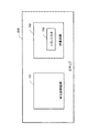
以下、図面を参照して本発明の実施の形態について説明する。図1は、本実施形態にかかる劣化診断回路100の全体構成例である。劣化診断回路100は、ローパスフィルタ部(RC時定数回路)1及び状態判定部2を備えている。ローパスフィルタ部1は、スイッチ部11と容量部12を有し、入力波形Vinに応じて出力Voutを出力する。状態判定部2は、ローパスフィルタ部1からの出力Voutと、参照電圧Vrefとに基づいて、スイッチ部11の状態値Vstateを生成する。
以下、図面を参照して本発明の実施の形態2について説明する。
2 状態判定部
3 供給電圧出力部
4 参照電圧出力部
11 スイッチ部
12 容量部
13 トランジスタ
14 コンデンサ
15 ゲート端子
16 ソース端子
17 ドレイン端子
20 コンパレータ回路
21、22 入力端子
31、32 セレクタ
33 定電圧出力部
34 波形出力部
35 制御部
100、101 劣化診断回路
102 対象回路
103 トランジスタ
200 ICチップ
Claims (7)
- スイッチ部及び当該スイッチ部に対して接続された容量部を含むと共に、入力波形に対してローパスフィルタ処理を実行するローパスフィルタ部と、
前記スイッチ部の制御端子に対して、前記スイッチ部をオン状態とする制御信号を選択的に供給する第1セレクタと、
前記ローパスフィルタ部に対して、前記入力波形を選択的に供給する第2セレクタと、
前記入力波形の入力に応じた前記ローパスフィルタ部の出力と参照電圧とに基づいて、前記ローパスフィルタ部に含まれる前記スイッチ部の状態を示す状態値を生成する状態判定部と、
を備える劣化診断回路。 - 前記第1セレクタは、前記スイッチ部の前記制御端子に対して、パルス波形を選択的に供給し、
前記第2セレクタは、前記ローパスフィルタ部に対して所定電位を選択的に供給することを特徴とする請求項1に記載の劣化診断回路。 - 前記第1及び第2セレクタの選択状態を制御する制御部を更に備え、
前記制御部は、前記スイッチ部の劣化診断時、前記第1セレクタに第1の所定電位を選択させ、かつ、前記第2セレクタに第1のパルス波形を選択させ、前記スイッチ部の劣化付与時、前記第1セレクタに第2のパルス波形を選択させ、かつ、前記第2セレクタに第2の所定電位を選択させることを特徴とする請求項2に記載の劣化診断回路。 - 前記劣化診断回路は、当該劣化診断回路が実装されるICチップに対して実装される他の回路の回路素子の劣化診断をするためのものである、請求項3に記載の劣化診断回路。
- 前記パルス波形のトグル率は、前記他の回路の回路素子に対して供給されるパルス波形のトグル率以上であることを特徴とする請求項4に記載の劣化診断回路。
- 前記参照電圧は、前記スイッチ部の劣化の判定に用いる電圧であって、
前記状態判定部は、前記ローパスフィルタ部の出力と前記参照電圧との大小関係に基づいて前記状態値を生成する、
請求項1ないし5のいずれか一項に記載の劣化診断回路。 - スイッチ部及び当該スイッチ部に対して接続された容量部を含むローパスフィルタ部が、入力波形に対してローパスフィルタ処理を実行するステップと、
第1セレクタが、前記スイッチ部の制御端子に対して、前記スイッチ部をオン状態とする制御信号を選択的に供給するステップと、
第2セレクタが、前記ローパスフィルタ部に対して、前記入力波形を選択的に供給するステップと、
前記ローパスフィルタ部に接続された状態判定部が、前記入力波形の入力に応じた前記ローパスフィルタ部の出力と参照電圧とに基づいて、前記スイッチ部の状態を示す状態値を生成するステップと、
を備えた劣化診断回路の動作方法。
Priority Applications (1)
| Application Number | Priority Date | Filing Date | Title |
|---|---|---|---|
| JP2011008556A JP5488480B2 (ja) | 2011-01-19 | 2011-01-19 | スイッチング素子の劣化診断回路及びその動作方法 |
Applications Claiming Priority (1)
| Application Number | Priority Date | Filing Date | Title |
|---|---|---|---|
| JP2011008556A JP5488480B2 (ja) | 2011-01-19 | 2011-01-19 | スイッチング素子の劣化診断回路及びその動作方法 |
Publications (2)
| Publication Number | Publication Date |
|---|---|
| JP2012149981A JP2012149981A (ja) | 2012-08-09 |
| JP5488480B2 true JP5488480B2 (ja) | 2014-05-14 |
Family
ID=46792359
Family Applications (1)
| Application Number | Title | Priority Date | Filing Date |
|---|---|---|---|
| JP2011008556A Expired - Fee Related JP5488480B2 (ja) | 2011-01-19 | 2011-01-19 | スイッチング素子の劣化診断回路及びその動作方法 |
Country Status (1)
| Country | Link |
|---|---|
| JP (1) | JP5488480B2 (ja) |
Family Cites Families (5)
| Publication number | Priority date | Publication date | Assignee | Title |
|---|---|---|---|---|
| US4720670A (en) * | 1986-12-23 | 1988-01-19 | International Business Machines Corporation | On chip performance predictor circuit |
| TW216472B (ja) * | 1991-12-18 | 1993-11-21 | Philips Nv | |
| JPH08125129A (ja) * | 1994-10-26 | 1996-05-17 | Matsushita Electric Ind Co Ltd | 半導体装置 |
| JPH1127128A (ja) * | 1997-07-08 | 1999-01-29 | Hitachi Ltd | 半導体集積回路装置 |
| JP4455434B2 (ja) * | 2005-07-12 | 2010-04-21 | 日本電信電話株式会社 | ミューティング判定回路およびミューティング回路 |
-
2011
- 2011-01-19 JP JP2011008556A patent/JP5488480B2/ja not_active Expired - Fee Related
Also Published As
| Publication number | Publication date |
|---|---|
| JP2012149981A (ja) | 2012-08-09 |
Similar Documents
| Publication | Publication Date | Title |
|---|---|---|
| TWI882977B (zh) | 積體電路i/o完整性和退化監控 | |
| TWI548886B (zh) | 老化偵測電路及其方法 | |
| JP6013221B2 (ja) | 集積回路装置 | |
| CN111999623A (zh) | 监控开关晶体管的系统和方法 | |
| JP5375438B2 (ja) | 劣化検出回路、劣化検出システム及び劣化検出方法 | |
| CN103650345A (zh) | 部件分析系统及方法 | |
| JP2017118414A (ja) | 半導体装置 | |
| JP2010249802A (ja) | 集積回路における外部端子の開放/短絡検査方法及び集積回路における外部端子の開放/短絡検査装置 | |
| JP4752904B2 (ja) | 温度測定回路、及び、方法 | |
| JP6409864B2 (ja) | 終端装置、終端制御方法、及び終端制御プログラムが記憶された記憶媒体 | |
| JP5488480B2 (ja) | スイッチング素子の劣化診断回路及びその動作方法 | |
| JP5707579B2 (ja) | パワー半導体用試験装置 | |
| JP6355745B2 (ja) | 従属性分離回路および当該従属性分離回路を備えた機能安全装置ならびに従属故障の検出方法 | |
| CN111103522B (zh) | 芯片与效能监控方法 | |
| JP6242183B2 (ja) | 半導体集積回路及び該半導体集積回路の試験方法並びに該半導体集積回路におけるラッシュカレントの抑制方法 | |
| US20090237145A1 (en) | Semiconductor device | |
| JP5915439B2 (ja) | 判定回路および半導体装置 | |
| JP5656760B2 (ja) | 半導体集積回路装置 | |
| JP4882937B2 (ja) | 半導体装置および半導体装置の検査方法 | |
| CN101859595B (zh) | 锁存装置及锁存方法 | |
| JP2010256026A (ja) | 電源解析容易化装置および電源解析容易化システム | |
| US10396648B2 (en) | Voltage adjusting circuit and method for adjusting voltage | |
| US12510589B2 (en) | Method of measuring chip characteristics, test device and non-transitory computer readable media | |
| JP6197573B2 (ja) | スイッチング素子検査方法及び電子回路ユニット | |
| JP5557783B2 (ja) | 半導体集積回路装置 |
Legal Events
| Date | Code | Title | Description |
|---|---|---|---|
| A977 | Report on retrieval |
Free format text: JAPANESE INTERMEDIATE CODE: A971007 Effective date: 20130201 |
|
| A131 | Notification of reasons for refusal |
Free format text: JAPANESE INTERMEDIATE CODE: A131 Effective date: 20130212 |
|
| A521 | Request for written amendment filed |
Free format text: JAPANESE INTERMEDIATE CODE: A523 Effective date: 20130403 |
|
| TRDD | Decision of grant or rejection written | ||
| A01 | Written decision to grant a patent or to grant a registration (utility model) |
Free format text: JAPANESE INTERMEDIATE CODE: A01 Effective date: 20140128 |
|
| A61 | First payment of annual fees (during grant procedure) |
Free format text: JAPANESE INTERMEDIATE CODE: A61 Effective date: 20140210 |
|
| R150 | Certificate of patent or registration of utility model |
Ref document number: 5488480 Country of ref document: JP Free format text: JAPANESE INTERMEDIATE CODE: R150 |
|
| LAPS | Cancellation because of no payment of annual fees |