JP5373733B2 - 垂直磁化磁性層を有する磁気トンネル接合構造 - Google Patents
垂直磁化磁性層を有する磁気トンネル接合構造 Download PDFInfo
- Publication number
- JP5373733B2 JP5373733B2 JP2010232405A JP2010232405A JP5373733B2 JP 5373733 B2 JP5373733 B2 JP 5373733B2 JP 2010232405 A JP2010232405 A JP 2010232405A JP 2010232405 A JP2010232405 A JP 2010232405A JP 5373733 B2 JP5373733 B2 JP 5373733B2
- Authority
- JP
- Japan
- Prior art keywords
- magnetic layer
- magnetic
- layer
- tunnel junction
- alloy
- Prior art date
- Legal status (The legal status is an assumption and is not a legal conclusion. Google has not performed a legal analysis and makes no representation as to the accuracy of the status listed.)
- Active
Links
- 230000005291 magnetic effect Effects 0.000 title claims abstract description 368
- 230000005415 magnetization Effects 0.000 claims abstract description 54
- 239000013078 crystal Substances 0.000 claims description 71
- 229910045601 alloy Inorganic materials 0.000 claims description 36
- 239000000956 alloy Substances 0.000 claims description 36
- 238000000926 separation method Methods 0.000 claims description 33
- 239000010409 thin film Substances 0.000 claims description 23
- 230000008878 coupling Effects 0.000 claims description 17
- 238000010168 coupling process Methods 0.000 claims description 17
- 238000005859 coupling reaction Methods 0.000 claims description 17
- 230000004888 barrier function Effects 0.000 claims description 13
- 229910052702 rhenium Inorganic materials 0.000 claims description 11
- 229910052703 rhodium Inorganic materials 0.000 claims description 10
- 229910052771 Terbium Inorganic materials 0.000 claims description 8
- 229910052804 chromium Inorganic materials 0.000 claims description 8
- 229910052759 nickel Inorganic materials 0.000 claims description 8
- 229910052763 palladium Inorganic materials 0.000 claims description 7
- 229910052697 platinum Inorganic materials 0.000 claims description 7
- 239000012212 insulator Substances 0.000 claims description 6
- 229910052761 rare earth metal Inorganic materials 0.000 claims description 5
- -1 rare earth transition metal Chemical class 0.000 claims description 5
- 229910052723 transition metal Inorganic materials 0.000 claims description 5
- 229910019222 CoCrPt Inorganic materials 0.000 claims description 4
- 229910018979 CoPt Inorganic materials 0.000 claims description 4
- 229910015187 FePd Inorganic materials 0.000 claims description 4
- 229910005335 FePt Inorganic materials 0.000 claims description 4
- 229910052688 Gadolinium Inorganic materials 0.000 claims description 4
- 229910016583 MnAl Inorganic materials 0.000 claims description 4
- 229910001260 Pt alloy Inorganic materials 0.000 claims description 4
- 229910052796 boron Inorganic materials 0.000 claims description 4
- RKTYLMNFRDHKIL-UHFFFAOYSA-N copper;5,10,15,20-tetraphenylporphyrin-22,24-diide Chemical compound [Cu+2].C1=CC(C(=C2C=CC([N-]2)=C(C=2C=CC=CC=2)C=2C=CC(N=2)=C(C=2C=CC=CC=2)C2=CC=C3[N-]2)C=2C=CC=CC=2)=NC1=C3C1=CC=CC=C1 RKTYLMNFRDHKIL-UHFFFAOYSA-N 0.000 claims description 4
- 229910052742 iron Inorganic materials 0.000 claims description 4
- 238000002955 isolation Methods 0.000 claims description 4
- 230000002441 reversible effect Effects 0.000 claims description 4
- 229910052707 ruthenium Inorganic materials 0.000 claims description 4
- 229910000938 samarium–cobalt magnet Inorganic materials 0.000 claims description 4
- 239000000126 substance Substances 0.000 claims description 4
- 229910018072 Al 2 O 3 Inorganic materials 0.000 claims description 3
- OKTJSMMVPCPJKN-UHFFFAOYSA-N Carbon Chemical compound [C] OKTJSMMVPCPJKN-UHFFFAOYSA-N 0.000 claims description 3
- 229910010413 TiO 2 Inorganic materials 0.000 claims description 3
- 229910052799 carbon Inorganic materials 0.000 claims description 3
- 229910052735 hafnium Inorganic materials 0.000 claims description 3
- 229910052741 iridium Inorganic materials 0.000 claims description 3
- 229910052762 osmium Inorganic materials 0.000 claims description 3
- 239000004065 semiconductor Substances 0.000 claims description 3
- 229910052721 tungsten Inorganic materials 0.000 claims description 3
- 229910052802 copper Inorganic materials 0.000 claims description 2
- 229910052737 gold Inorganic materials 0.000 claims description 2
- 229910052715 tantalum Inorganic materials 0.000 claims description 2
- 239000000463 material Substances 0.000 description 10
- 238000000034 method Methods 0.000 description 9
- 239000000470 constituent Substances 0.000 description 6
- 238000010438 heat treatment Methods 0.000 description 5
- 229910019236 CoFeB Inorganic materials 0.000 description 4
- 230000001427 coherent effect Effects 0.000 description 4
- 230000015654 memory Effects 0.000 description 4
- 230000010355 oscillation Effects 0.000 description 3
- 230000008569 process Effects 0.000 description 3
- 230000008859 change Effects 0.000 description 2
- 239000003302 ferromagnetic material Substances 0.000 description 2
- 239000010408 film Substances 0.000 description 2
- 239000003574 free electron Substances 0.000 description 2
- 238000001451 molecular beam epitaxy Methods 0.000 description 2
- 230000005641 tunneling Effects 0.000 description 2
- 230000009471 action Effects 0.000 description 1
- 230000005290 antiferromagnetic effect Effects 0.000 description 1
- 230000015572 biosynthetic process Effects 0.000 description 1
- 238000002425 crystallisation Methods 0.000 description 1
- 230000008025 crystallization Effects 0.000 description 1
- 230000007423 decrease Effects 0.000 description 1
- 230000000694 effects Effects 0.000 description 1
- 230000001747 exhibiting effect Effects 0.000 description 1
- 230000005294 ferromagnetic effect Effects 0.000 description 1
- 230000006698 induction Effects 0.000 description 1
- 230000010354 integration Effects 0.000 description 1
- 238000004519 manufacturing process Methods 0.000 description 1
- 238000002844 melting Methods 0.000 description 1
- 230000008018 melting Effects 0.000 description 1
- 230000004048 modification Effects 0.000 description 1
- 238000012986 modification Methods 0.000 description 1
- 230000010287 polarization Effects 0.000 description 1
- 230000035945 sensitivity Effects 0.000 description 1
- 230000001568 sexual effect Effects 0.000 description 1
- 230000005428 wave function Effects 0.000 description 1
Images

Classifications
-
- H—ELECTRICITY
- H10—SEMICONDUCTOR DEVICES; ELECTRIC SOLID-STATE DEVICES NOT OTHERWISE PROVIDED FOR
- H10N—ELECTRIC SOLID-STATE DEVICES NOT OTHERWISE PROVIDED FOR
- H10N50/00—Galvanomagnetic devices
- H10N50/10—Magnetoresistive devices
-
- G—PHYSICS
- G11—INFORMATION STORAGE
- G11C—STATIC STORES
- G11C11/00—Digital stores characterised by the use of particular electric or magnetic storage elements; Storage elements therefor
- G11C11/02—Digital stores characterised by the use of particular electric or magnetic storage elements; Storage elements therefor using magnetic elements
- G11C11/14—Digital stores characterised by the use of particular electric or magnetic storage elements; Storage elements therefor using magnetic elements using thin-film elements
- G11C11/15—Digital stores characterised by the use of particular electric or magnetic storage elements; Storage elements therefor using magnetic elements using thin-film elements using multiple magnetic layers
-
- B—PERFORMING OPERATIONS; TRANSPORTING
- B82—NANOTECHNOLOGY
- B82Y—SPECIFIC USES OR APPLICATIONS OF NANOSTRUCTURES; MEASUREMENT OR ANALYSIS OF NANOSTRUCTURES; MANUFACTURE OR TREATMENT OF NANOSTRUCTURES
- B82Y10/00—Nanotechnology for information processing, storage or transmission, e.g. quantum computing or single electron logic
-
- B—PERFORMING OPERATIONS; TRANSPORTING
- B82—NANOTECHNOLOGY
- B82Y—SPECIFIC USES OR APPLICATIONS OF NANOSTRUCTURES; MEASUREMENT OR ANALYSIS OF NANOSTRUCTURES; MANUFACTURE OR TREATMENT OF NANOSTRUCTURES
- B82Y25/00—Nanomagnetism, e.g. magnetoimpedance, anisotropic magnetoresistance, giant magnetoresistance or tunneling magnetoresistance
-
- G—PHYSICS
- G11—INFORMATION STORAGE
- G11B—INFORMATION STORAGE BASED ON RELATIVE MOVEMENT BETWEEN RECORD CARRIER AND TRANSDUCER
- G11B5/00—Recording by magnetisation or demagnetisation of a record carrier; Reproducing by magnetic means; Record carriers therefor
- G11B5/127—Structure or manufacture of heads, e.g. inductive
- G11B5/33—Structure or manufacture of flux-sensitive heads, i.e. for reproduction only; Combination of such heads with means for recording or erasing only
- G11B5/39—Structure or manufacture of flux-sensitive heads, i.e. for reproduction only; Combination of such heads with means for recording or erasing only using magneto-resistive devices or effects
- G11B5/3903—Structure or manufacture of flux-sensitive heads, i.e. for reproduction only; Combination of such heads with means for recording or erasing only using magneto-resistive devices or effects using magnetic thin film layers or their effects, the films being part of integrated structures
- G11B5/3906—Details related to the use of magnetic thin film layers or to their effects
- G11B5/3909—Arrangements using a magnetic tunnel junction
-
- G—PHYSICS
- G11—INFORMATION STORAGE
- G11C—STATIC STORES
- G11C11/00—Digital stores characterised by the use of particular electric or magnetic storage elements; Storage elements therefor
- G11C11/02—Digital stores characterised by the use of particular electric or magnetic storage elements; Storage elements therefor using magnetic elements
- G11C11/16—Digital stores characterised by the use of particular electric or magnetic storage elements; Storage elements therefor using magnetic elements using elements in which the storage effect is based on magnetic spin effect
- G11C11/161—Digital stores characterised by the use of particular electric or magnetic storage elements; Storage elements therefor using magnetic elements using elements in which the storage effect is based on magnetic spin effect details concerning the memory cell structure, e.g. the layers of the ferromagnetic memory cell
-
- H—ELECTRICITY
- H01—ELECTRIC ELEMENTS
- H01F—MAGNETS; INDUCTANCES; TRANSFORMERS; SELECTION OF MATERIALS FOR THEIR MAGNETIC PROPERTIES
- H01F10/00—Thin magnetic films, e.g. of one-domain structure
- H01F10/32—Spin-exchange-coupled multilayers, e.g. nanostructured superlattices
- H01F10/324—Exchange coupling of magnetic film pairs via a very thin non-magnetic spacer, e.g. by exchange with conduction electrons of the spacer
- H01F10/3254—Exchange coupling of magnetic film pairs via a very thin non-magnetic spacer, e.g. by exchange with conduction electrons of the spacer the spacer being semiconducting or insulating, e.g. for spin tunnel junction [STJ]
-
- H—ELECTRICITY
- H01—ELECTRIC ELEMENTS
- H01F—MAGNETS; INDUCTANCES; TRANSFORMERS; SELECTION OF MATERIALS FOR THEIR MAGNETIC PROPERTIES
- H01F10/00—Thin magnetic films, e.g. of one-domain structure
- H01F10/32—Spin-exchange-coupled multilayers, e.g. nanostructured superlattices
- H01F10/324—Exchange coupling of magnetic film pairs via a very thin non-magnetic spacer, e.g. by exchange with conduction electrons of the spacer
- H01F10/3268—Exchange coupling of magnetic film pairs via a very thin non-magnetic spacer, e.g. by exchange with conduction electrons of the spacer the exchange coupling being asymmetric, e.g. by use of additional pinning, by using antiferromagnetic or ferromagnetic coupling interface, i.e. so-called spin-valve [SV] structure, e.g. NiFe/Cu/NiFe/FeMn
-
- H—ELECTRICITY
- H01—ELECTRIC ELEMENTS
- H01F—MAGNETS; INDUCTANCES; TRANSFORMERS; SELECTION OF MATERIALS FOR THEIR MAGNETIC PROPERTIES
- H01F10/00—Thin magnetic films, e.g. of one-domain structure
- H01F10/32—Spin-exchange-coupled multilayers, e.g. nanostructured superlattices
- H01F10/324—Exchange coupling of magnetic film pairs via a very thin non-magnetic spacer, e.g. by exchange with conduction electrons of the spacer
- H01F10/3286—Spin-exchange coupled multilayers having at least one layer with perpendicular magnetic anisotropy
-
- G—PHYSICS
- G11—INFORMATION STORAGE
- G11B—INFORMATION STORAGE BASED ON RELATIVE MOVEMENT BETWEEN RECORD CARRIER AND TRANSDUCER
- G11B5/00—Recording by magnetisation or demagnetisation of a record carrier; Reproducing by magnetic means; Record carriers therefor
- G11B5/127—Structure or manufacture of heads, e.g. inductive
- G11B5/33—Structure or manufacture of flux-sensitive heads, i.e. for reproduction only; Combination of such heads with means for recording or erasing only
- G11B5/39—Structure or manufacture of flux-sensitive heads, i.e. for reproduction only; Combination of such heads with means for recording or erasing only using magneto-resistive devices or effects
- G11B5/3903—Structure or manufacture of flux-sensitive heads, i.e. for reproduction only; Combination of such heads with means for recording or erasing only using magneto-resistive devices or effects using magnetic thin film layers or their effects, the films being part of integrated structures
- G11B5/3906—Details related to the use of magnetic thin film layers or to their effects
Landscapes
- Engineering & Computer Science (AREA)
- Chemical & Material Sciences (AREA)
- Crystallography & Structural Chemistry (AREA)
- Nanotechnology (AREA)
- Power Engineering (AREA)
- Computer Hardware Design (AREA)
- Manufacturing & Machinery (AREA)
- Physics & Mathematics (AREA)
- Mathematical Physics (AREA)
- Theoretical Computer Science (AREA)
- Hall/Mr Elements (AREA)
- Mram Or Spin Memory Techniques (AREA)
Description
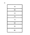
20 第2磁性層
30 第3磁性層
40 第4磁性層
50 第1結晶構造分離層
60 第2結晶構造分離層
70 非磁性層(トンネル障壁層)
80 下地層(バッファ層)
Claims (14)
- 固定された磁化方向を有する第1磁性層と、
反転可能な磁化方向を有する第2磁性層と、
前記第1磁性層と前記第2磁性層との間に形成される非磁性層(トンネル障壁層)と、
前記第1磁性層との磁性結合により前記第1磁性層の磁化方向が薄膜面に対して垂直となるようにし、垂直磁気異方性エネルギーが水平磁気異方性エネルギーより大きい第3磁性層と、
前記第1磁性層と前記第3磁性層との間に形成され、前記第1磁性層の結晶配向性と前記第3磁性層の結晶配向性を分離する第1結晶構造分離層と、
前記第2磁性層との磁性結合により前記第2磁性層の磁化方向が薄膜面に対して垂直となるようにし、垂直磁気異方性エネルギーが水平磁気異方性エネルギーより大きい第4磁性層と、
前記第2磁性層と前記第4磁性層との間に形成され、前記第2磁性層の結晶配向性と前記第4磁性層の結晶配向性を分離する第2結晶構造分離層と
を含み、
前記第1磁性層と前記第2磁性層の少なくとも一方の磁性層は、体心立方格子構造を有し、前記第3磁性層と前記第4磁性層の少なくとも一方の磁性層は、面心立方格子構造、面心正方格子構造、又は稠密六方格子構造を有し、
前記第1結晶構造分離層と前記第2結晶構造分離層の少なくとも一方の結晶構造分離層は、200〜600℃の温度で熱処理しても非晶質構造が維持される物質を含み、
前記第1結晶構造分離層と前記第2結晶構造分離層の少なくとも一方の結晶構造分離層は、Ru、Ta、Re、Hf、W、Os、Ir、及びRhからなる群から独立して選択された少なくとも1つを含み、
前記第3磁性層の下に形成される下地層をさらに含み、
前記下地層は、Au、Cu、Pd、Pt、Ta、及びダイヤモンド状炭素からなる群から選択された少なくとも1つを含むことを特徴とする磁気トンネル接合構造。 - 前記非磁性層は、絶縁体又は半導体を含み、前記絶縁体は、MgO、Al2O3、HfO2、TiO2、Y2O3、及びYb2O3からなる群から選択された少なくとも1つであることを特徴とする請求項1に記載の磁気トンネル接合構造。
- 前記第1磁性層は、磁性層/非磁性層/磁性層の積層構造を有することを特徴とする請求項1に記載の磁気トンネル接合構造。
- 前記第1磁性層と前記第2磁性層の少なくとも一方の磁性層は、FeX、CoX、NiX、FeCoX、CoNiX、又はNiFeX(ここで、XはB、Re、Rh、Cr、Cu、Gd、及びTbからなる群から選択された少なくとも1つ)を含むことを特徴とする請求項1に記載の磁気トンネル接合構造。
- 前記第3磁性層及び前記第4磁性層の磁化容易軸は、それぞれ前記第1磁性層及び前記第2磁性層の平面に対して垂直方向に配向されることを特徴とする請求項1に記載の磁気トンネル接合構造。
- 前記第3磁性層及び前記第4磁性層の磁化方向がそれぞれ前記第3磁性層及び前記第4磁性層の平面に対して傾斜した角度は、60゜≦θ≦120゜であることを特徴とする請求項1に記載の磁気トンネル接合構造。
- 前記第3磁性層と前記第4磁性層の少なくとも一方の磁性層は、面心正方構造を有する合金を含むことを特徴とする請求項1に記載の磁気トンネル接合構造。
- 前記面心正方構造を有する合金は、FePt、CoPt、FePd、及びMnAlからなる群から選択された少なくとも1つであることを特徴とする請求項7に記載の磁気トンネル接合構造。
- 前記第3磁性層と前記第4磁性層の少なくとも一方の磁性層は、稠密六方構造を有する合金を含むことを特徴とする請求項1に記載の磁気トンネル接合構造。
- 前記稠密六方構造を有する合金は、Co3Pt合金又はCoCrPt合金であることを特徴とする請求項9に記載の磁気トンネル接合構造。
- 前記第3磁性層と前記第4磁性層の少なくとも一方の磁性層は、希土類遷移金属合金を含むことを特徴とする請求項1に記載の磁気トンネル接合構造。
- 前記希土類遷移金属合金は、Fe14Nd2B又はSmCo5であることを特徴とする請求項11に記載の磁気トンネル接合構造。
- 前記第3磁性層と前記第4磁性層の少なくとも一方の磁性層は、多層薄膜を含むことを特徴とする請求項1に記載の磁気トンネル接合構造。
- 前記多層薄膜は、[Co/Pt]n、[CoX合金/Pt]n、[Co/Pd]n、[CoX合金/Pd]n、[Co/Ni]n、[CoX合金/Ni]n、又は[Ni/Pt]nであり、前記nは、1から10の数字であり、前記Xは、Fe、Ni、Cr、Ru、Re、Rh、Gd、及びTbからなる群から選択された少なくとも1つであることを特徴とする請求項13に記載の磁気トンネル接合構造。
Applications Claiming Priority (2)
| Application Number | Priority Date | Filing Date | Title |
|---|---|---|---|
| KR1020090099432A KR101096517B1 (ko) | 2009-10-19 | 2009-10-19 | 수직 자화 자성층을 갖는 자기 터널 접합 구조 |
| KR10-2009-0099432 | 2009-10-19 |
Publications (2)
| Publication Number | Publication Date |
|---|---|
| JP2011086944A JP2011086944A (ja) | 2011-04-28 |
| JP5373733B2 true JP5373733B2 (ja) | 2013-12-18 |
Family
ID=43878643
Family Applications (1)
| Application Number | Title | Priority Date | Filing Date |
|---|---|---|---|
| JP2010232405A Active JP5373733B2 (ja) | 2009-10-19 | 2010-10-15 | 垂直磁化磁性層を有する磁気トンネル接合構造 |
Country Status (3)
| Country | Link |
|---|---|
| US (1) | US8319297B2 (ja) |
| JP (1) | JP5373733B2 (ja) |
| KR (1) | KR101096517B1 (ja) |
Families Citing this family (14)
| Publication number | Priority date | Publication date | Assignee | Title |
|---|---|---|---|---|
| JP2010263131A (ja) * | 2009-05-08 | 2010-11-18 | Elpida Memory Inc | 超格子デバイス及びその製造方法、並びに、超格子デバイスを含む固体メモリ、データ処理システム及びデータ処理装置 |
| KR101658394B1 (ko) * | 2009-12-15 | 2016-09-22 | 삼성전자 주식회사 | 자기터널접합 소자 및 그 제조방법과 자기터널접합 소자를 포함하는 전자소자 |
| JP5161951B2 (ja) | 2010-11-26 | 2013-03-13 | 株式会社東芝 | スピントルク発振子および磁気記録装置 |
| US8508006B2 (en) * | 2011-05-10 | 2013-08-13 | Magic Technologies, Inc. | Co/Ni multilayers with improved out-of-plane anisotropy for magnetic device applications |
| US8836056B2 (en) * | 2012-09-26 | 2014-09-16 | Intel Corporation | Perpendicular MTJ stacks with magnetic anisotropy enhancing layer and crystallization barrier layer |
| JP5957375B2 (ja) * | 2012-11-30 | 2016-07-27 | 株式会社日立製作所 | 相変化メモリ |
| JP6342113B2 (ja) * | 2012-12-19 | 2018-06-13 | サムスン エレクトロニクス カンパニー リミテッド | 改良型特性を有する磁気接合を提供する方法およびシステム |
| JP6119051B2 (ja) * | 2013-08-02 | 2017-04-26 | 株式会社東芝 | 磁気抵抗素子および磁気メモリ |
| US9306155B2 (en) | 2013-11-11 | 2016-04-05 | Samsung Electronics Co., Ltd. | Method and system for providing a bulk perpendicular magnetic anisotropy free layer in a perpendicular magnetic junction usable in spin transfer torque magnetic random access memory applications |
| KR102126975B1 (ko) * | 2013-12-09 | 2020-06-25 | 삼성전자주식회사 | 자기 기억 소자 및 그 제조 방법 |
| KR101549625B1 (ko) * | 2014-04-18 | 2015-09-04 | 한양대학교 산학협력단 | 메모리 소자 |
| WO2016148392A1 (ko) * | 2015-03-18 | 2016-09-22 | 한양대학교 산학협력단 | 메모리 소자 |
| US10121960B2 (en) | 2016-10-17 | 2018-11-06 | Samsung Electronics Co., Ltd. | Method and system for providing magnetic junctions usable in spin transfer torque applications utilizing interstitial glass-forming agent(s) |
| KR102073368B1 (ko) * | 2018-07-23 | 2020-02-04 | 한국과학기술연구원 | 자기기록장치 |
Family Cites Families (10)
| Publication number | Priority date | Publication date | Assignee | Title |
|---|---|---|---|---|
| JP3293437B2 (ja) * | 1995-12-19 | 2002-06-17 | 松下電器産業株式会社 | 磁気抵抗効果素子、磁気抵抗効果型ヘッド及びメモリー素子 |
| US6798624B2 (en) * | 2001-03-15 | 2004-09-28 | Seagate Technology Llc | Magnetization sensor for sensing the write field characteristics of a perpendicular or longitudinal recording head |
| US6967863B2 (en) | 2004-02-25 | 2005-11-22 | Grandis, Inc. | Perpendicular magnetization magnetic element utilizing spin transfer |
| KR100707170B1 (ko) * | 2004-08-23 | 2007-04-13 | 삼성전자주식회사 | 균일한 스위칭 특성을 가지며 저 전류 스위칭이 가능한자기 메모리 소자 및 그 동작방법 |
| JP5096702B2 (ja) * | 2005-07-28 | 2012-12-12 | 株式会社日立製作所 | 磁気抵抗効果素子及びそれを搭載した不揮発性磁気メモリ |
| US20070096229A1 (en) * | 2005-10-28 | 2007-05-03 | Masatoshi Yoshikawa | Magnetoresistive element and magnetic memory device |
| KR20080029819A (ko) * | 2006-09-29 | 2008-04-03 | 가부시끼가이샤 도시바 | 자기저항 효과 소자 및 이를 이용한 자기 랜덤 액세스메모리 |
| JP4738395B2 (ja) * | 2007-09-25 | 2011-08-03 | 株式会社東芝 | 磁気抵抗効果素子およびそれを用いた磁気ランダムアクセスメモリ |
| KR101178767B1 (ko) | 2008-10-30 | 2012-09-07 | 한국과학기술연구원 | 이중 자기 이방성 자유층을 갖는 자기 터널 접합 구조 |
| US8445979B2 (en) * | 2009-09-11 | 2013-05-21 | Samsung Electronics Co., Ltd. | Magnetic memory devices including magnetic layers separated by tunnel barriers |
-
2009
- 2009-10-19 KR KR1020090099432A patent/KR101096517B1/ko active Active
-
2010
- 2010-10-05 US US12/897,914 patent/US8319297B2/en not_active Expired - Fee Related
- 2010-10-15 JP JP2010232405A patent/JP5373733B2/ja active Active
Also Published As
| Publication number | Publication date |
|---|---|
| KR101096517B1 (ko) | 2011-12-20 |
| JP2011086944A (ja) | 2011-04-28 |
| US20110089508A1 (en) | 2011-04-21 |
| US8319297B2 (en) | 2012-11-27 |
| KR20110042657A (ko) | 2011-04-27 |
Similar Documents
| Publication | Publication Date | Title |
|---|---|---|
| JP5113135B2 (ja) | 二重磁気異方性自由層を有する磁気トンネル接合構造 | |
| KR101096517B1 (ko) | 수직 자화 자성층을 갖는 자기 터널 접합 구조 | |
| US10734574B2 (en) | Method of manufacturing high annealing temperature perpendicular magnetic anisotropy structure for magnetic random access memory | |
| US8184411B2 (en) | MTJ incorporating CoFe/Ni multilayer film with perpendicular magnetic anisotropy for MRAM application | |
| JP5534766B2 (ja) | スピントロニック素子のスピンバルブ構造およびその形成方法、ボトム型スピンバルブ構造、ならびにマイクロ波アシスト磁気記録用スピントロニック素子 | |
| US8064244B2 (en) | Thin seeded Co/Ni multilayer film with perpendicular anisotropy for spintronic device applications | |
| US9349396B2 (en) | CoFe/Ni multilayer film with perpendicular anisotropy for microwave assisted magnetic recording | |
| US7813202B2 (en) | Thin-film magnetic device with strong spin polarization perpendicular to the plane of the layers, magnetic tunnel junction and spin valve using such a device | |
| JP5579175B2 (ja) | 磁気抵抗効果素子及びそれを用いたランダムアクセスメモリ | |
| US9680088B2 (en) | Ferromagnetic tunnel junction element and method of driving ferromagnetic tunnel junction element | |
| WO2011001746A1 (ja) | 磁気メモリー素子及びその駆動方法 | |
| JP5987613B2 (ja) | 記憶素子、記憶装置、磁気ヘッド | |
| JP2007525033A (ja) | スピン・トランスファによる垂直磁化磁気素子 | |
| JP2012015213A (ja) | 記憶素子、記憶素子の製造方法、及び、メモリ | |
| JPWO2012004883A1 (ja) | 磁気抵抗効果素子及びそれを用いたランダムアクセスメモリ | |
| JP2014072393A (ja) | 記憶素子、記憶装置、磁気ヘッド | |
| Yuasa | Magnetic properties of materials for MRAM |
Legal Events
| Date | Code | Title | Description |
|---|---|---|---|
| A977 | Report on retrieval |
Free format text: JAPANESE INTERMEDIATE CODE: A971007 Effective date: 20121102 |
|
| A131 | Notification of reasons for refusal |
Free format text: JAPANESE INTERMEDIATE CODE: A131 Effective date: 20121106 |
|
| A521 | Request for written amendment filed |
Free format text: JAPANESE INTERMEDIATE CODE: A523 Effective date: 20130206 |
|
| TRDD | Decision of grant or rejection written | ||
| A01 | Written decision to grant a patent or to grant a registration (utility model) |
Free format text: JAPANESE INTERMEDIATE CODE: A01 Effective date: 20130820 |
|
| A61 | First payment of annual fees (during grant procedure) |
Free format text: JAPANESE INTERMEDIATE CODE: A61 Effective date: 20130919 |
|
| R150 | Certificate of patent or registration of utility model |
Ref document number: 5373733 Country of ref document: JP Free format text: JAPANESE INTERMEDIATE CODE: R150 Free format text: JAPANESE INTERMEDIATE CODE: R150 |
|
| R250 | Receipt of annual fees |
Free format text: JAPANESE INTERMEDIATE CODE: R250 |
|
| R250 | Receipt of annual fees |
Free format text: JAPANESE INTERMEDIATE CODE: R250 |
|
| R250 | Receipt of annual fees |
Free format text: JAPANESE INTERMEDIATE CODE: R250 |
|
| R250 | Receipt of annual fees |
Free format text: JAPANESE INTERMEDIATE CODE: R250 |
|
| R250 | Receipt of annual fees |
Free format text: JAPANESE INTERMEDIATE CODE: R250 |
|
| R250 | Receipt of annual fees |
Free format text: JAPANESE INTERMEDIATE CODE: R250 |
|
| R250 | Receipt of annual fees |
Free format text: JAPANESE INTERMEDIATE CODE: R250 |
|
| R250 | Receipt of annual fees |
Free format text: JAPANESE INTERMEDIATE CODE: R250 |
|
| R250 | Receipt of annual fees |
Free format text: JAPANESE INTERMEDIATE CODE: R250 |