JP5367587B2 - 太陽電池モジュール及び太陽電池 - Google Patents
太陽電池モジュール及び太陽電池 Download PDFInfo
- Publication number
- JP5367587B2 JP5367587B2 JP2009552536A JP2009552536A JP5367587B2 JP 5367587 B2 JP5367587 B2 JP 5367587B2 JP 2009552536 A JP2009552536 A JP 2009552536A JP 2009552536 A JP2009552536 A JP 2009552536A JP 5367587 B2 JP5367587 B2 JP 5367587B2
- Authority
- JP
- Japan
- Prior art keywords
- solar cell
- electrode
- area
- region
- ratio
- Prior art date
- Legal status (The legal status is an assumption and is not a legal conclusion. Google has not performed a legal analysis and makes no representation as to the accuracy of the status listed.)
- Active
Links
Images


Classifications
-
- H—ELECTRICITY
- H10—SEMICONDUCTOR DEVICES; ELECTRIC SOLID-STATE DEVICES NOT OTHERWISE PROVIDED FOR
- H10F—INORGANIC SEMICONDUCTOR DEVICES SENSITIVE TO INFRARED RADIATION, LIGHT, ELECTROMAGNETIC RADIATION OF SHORTER WAVELENGTH OR CORPUSCULAR RADIATION
- H10F77/00—Constructional details of devices covered by this subclass
- H10F77/20—Electrodes
- H10F77/206—Electrodes for devices having potential barriers
- H10F77/211—Electrodes for devices having potential barriers for photovoltaic cells
- H10F77/215—Geometries of grid contacts
-
- H—ELECTRICITY
- H10—SEMICONDUCTOR DEVICES; ELECTRIC SOLID-STATE DEVICES NOT OTHERWISE PROVIDED FOR
- H10F—INORGANIC SEMICONDUCTOR DEVICES SENSITIVE TO INFRARED RADIATION, LIGHT, ELECTROMAGNETIC RADIATION OF SHORTER WAVELENGTH OR CORPUSCULAR RADIATION
- H10F10/00—Individual photovoltaic cells, e.g. solar cells
- H10F10/10—Individual photovoltaic cells, e.g. solar cells having potential barriers
- H10F10/16—Photovoltaic cells having only PN heterojunction potential barriers
- H10F10/164—Photovoltaic cells having only PN heterojunction potential barriers comprising heterojunctions with Group IV materials, e.g. ITO/Si or GaAs/SiGe photovoltaic cells
- H10F10/165—Photovoltaic cells having only PN heterojunction potential barriers comprising heterojunctions with Group IV materials, e.g. ITO/Si or GaAs/SiGe photovoltaic cells the heterojunctions being Group IV-IV heterojunctions, e.g. Si/Ge, SiGe/Si or Si/SiC photovoltaic cells
- H10F10/166—Photovoltaic cells having only PN heterojunction potential barriers comprising heterojunctions with Group IV materials, e.g. ITO/Si or GaAs/SiGe photovoltaic cells the heterojunctions being Group IV-IV heterojunctions, e.g. Si/Ge, SiGe/Si or Si/SiC photovoltaic cells the Group IV-IV heterojunctions being heterojunctions of crystalline and amorphous materials, e.g. silicon heterojunction [SHJ] photovoltaic cells
-
- H—ELECTRICITY
- H10—SEMICONDUCTOR DEVICES; ELECTRIC SOLID-STATE DEVICES NOT OTHERWISE PROVIDED FOR
- H10F—INORGANIC SEMICONDUCTOR DEVICES SENSITIVE TO INFRARED RADIATION, LIGHT, ELECTROMAGNETIC RADIATION OF SHORTER WAVELENGTH OR CORPUSCULAR RADIATION
- H10F19/00—Integrated devices, or assemblies of multiple devices, comprising at least one photovoltaic cell covered by group H10F10/00, e.g. photovoltaic modules
- H10F19/90—Structures for connecting between photovoltaic cells, e.g. interconnections or insulating spacers
- H10F19/902—Structures for connecting between photovoltaic cells, e.g. interconnections or insulating spacers for series or parallel connection of photovoltaic cells
-
- Y—GENERAL TAGGING OF NEW TECHNOLOGICAL DEVELOPMENTS; GENERAL TAGGING OF CROSS-SECTIONAL TECHNOLOGIES SPANNING OVER SEVERAL SECTIONS OF THE IPC; TECHNICAL SUBJECTS COVERED BY FORMER USPC CROSS-REFERENCE ART COLLECTIONS [XRACs] AND DIGESTS
- Y02—TECHNOLOGIES OR APPLICATIONS FOR MITIGATION OR ADAPTATION AGAINST CLIMATE CHANGE
- Y02E—REDUCTION OF GREENHOUSE GAS [GHG] EMISSIONS, RELATED TO ENERGY GENERATION, TRANSMISSION OR DISTRIBUTION
- Y02E10/00—Energy generation through renewable energy sources
- Y02E10/50—Photovoltaic [PV] energy
Landscapes
- Photovoltaic Devices (AREA)
Description
(太陽電池モジュールの概略構成)
本発明の第1実施形態に係る太陽電池モジュール1の概略構成について、図1及び図2を参照しながら説明する。図1は、本実施形態に係る太陽電池モジュール1の側面図である。図2(a)は、太陽電池モジュール1の受光面側の平面図である。図2(b)は、太陽電池モジュール1の裏面側の平面図である。
次に、第1電極12及び第2電極13の構成について、図3を参照しながら説明する。図3(a)は、太陽電池10の第1主面(受光面)A側の平面図である。図3(b)は、太陽電池10の第2主面(裏面)B側の平面図である。
以上より、第1電極12の形成面積と、第2電極13の形成面積との間には、次の関係が成立する。
次に、本実施形態に係る太陽電池モジュール1の製造方法について説明する。
本実施形態に係る太陽電池10において、第1電極12は、第1接続部12aと第1露出部12bとを有し、第2電極13は、第2接続部13aと第2露出部13bとを有する。この場合において、上記第1の関係((v/w)<1)と、上記第2の関係((v/w)<(x/y))とが成立する。
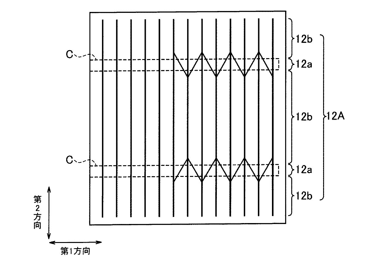
次に、本発明の第2実施形態について、図面を参照しながら説明する。本実施形態と上記第1実施形態との相違点は、領域Cにおける単位面積当たりの電極形成面積を、領域Dに近づけている点である。その他の点については上記第1実施形態と同様であるため、以下、相違点について主に説明する。
本実施形態に係る第1電極12及び第2電極13の構成について、図4を参照しながら説明する。図4(a)は、太陽電池10の第1主面(受光面)A側の平面図である。図4(b)は、太陽電池10の第2主面(裏面)B側の平面図である。
以上より、本実施形態においても、第1電極12の形成面積と第2電極13の形成面積との間には、上記第1実施形態と同様に、第1の関係((v/w)<1)と第2の関係((v/w)<(x/y))とが成立する。
本実施形態に係る太陽電池10においても、上記第1の関係((v/w)<1)と、上記第2の関係((v/w)<(x/y))とが成立する。
次に、本発明の第3実施形態について、図面を参照しながら説明する。本実施形態と上記第2実施形態との相違点は、領域Cに島状部材14が形成される点である。その他の点については上記第2実施形態と同様であるため、以下、相違点について主に説明する。
本実施形態に係る第1電極12及び第2電極13の構成について、図5を参照しながら説明する。図5(a)は、太陽電池10の第1主面A側の平面図である。図5(b)は、太陽電池10の第2主面B側の平面図である。
以上より、第1部材群12´の形成面積と複数本の第2細線電極13Aの形成面積との間において、上記第2実施形態と同様に、第1の関係((v/w)<1)と第2の関係((v/w)<(x/y))とが成立する。
本実施形態に係る太陽電池10においても、上記第1の関係((v/w)<1)と、上記第2の関係((v/w)<(x/y))とが成立する。
本発明は上記の実施形態によって記載したが、この開示の一部をなす論述及び図面はこの発明を限定するものであると理解すべきではない。この開示から当業者には様々な代替実施形態、実施例及び運用技術が明らかとなろう。
まず、寸法108mm角、厚み150μm、抵抗率1Ωcmのn型単結晶シリコン基板を準備した。
次に、実施例2に係る太陽電池モジュールを1000枚作製した。実施例2と上記実施例1との相違点は、銀ペーストを図4に示すパターンで印刷した点である。
次に、比較例1に係る太陽電池モジュールを1000枚作製した。比較例1と上記実施例1との相違点は、配線材を接続する領域において細線電極を分岐又は結合させない点である。
実施例1、実施例2及び比較例に係る太陽電池について、恒温槽を用いて温度サイクル試験を行い、試験後における太陽電池の出力低下率を比較した。測定結果を下表に示す。なお、下表中の数値は、1000枚の太陽電池についての平均値である。
Claims (7)
- 太陽電池と、
前記太陽電池の受光面の第1領域を覆う一の配線材と、
前記太陽電池の前記受光面の反対側に設けられる裏面の第2領域を覆う他の配線材と、を備え、
前記太陽電池は、
前記受光面上に形成される複数本の第1細線電極を少なくとも含む第1電極と、
前記裏面上に形成される第2電極と、
を有し、
前記第1電極は、
前記第1領域内に設けられ、前記一の配線材に接続される第1接続部と、
前記第1領域外に設けられ、前記一の配線材から露出する一群の第1露出部と、
を有し、
前記第2電極は、
前記第2領域内に設けられ、前記他の配線材に接続される第2接続部と、
前記第2領域外に設けられ、前記他の配線材から露出する第2露出部と、
を有し、
前記受光面の面積に対する前記第1露出部が形成される面積の比率である第1比率は、前記裏面の面積に対する前記第2露出部が形成される面積の比率である第2比率より小さく、
前記第1比率の前記第2比率に対する比は、前記受光面のうち前記第1領域の面積に対する前記第1接続部の面積の比率である第3比率の、前記裏面のうち前記第2領域の面積に対する前記第2接続部の面積の比率である第4比率に対する比よりも小さく、
前記第3比率及び前記第4比率のうち少なくともいずれか一方は1より小さい
ことを特徴とする太陽電池モジュール。 - 前記第2電極は、前記複数本の第2細線電極を有し、
前記複数本の第2細線電極は、前記第2接続部と前記第2露出部とを有する
ことを特徴とする請求項1に記載の太陽電池モジュール。 - 前記第1接続部は、前記一の配線材に直接接触して接続される
ことを特徴とする請求項1又は2に記載の太陽電池モジュール。 - 前記第2接続部は、前記他の配線材に直接接触して接続される
ことを特徴とする請求項1又は2に記載の太陽電池モジュール。 - 前記複数本の第2細線電極のうち少なくとも2本の第2細線電極は、前記第2領域において1本に結合される
ことを特徴とする請求項2に記載の太陽電池モジュール。 - 前記複数本の第1細線電極のうち少なくとも1本の第1細線電極は、前記第1領域において複数本に分岐される
ことを特徴とする請求項1又は2に記載の太陽電池モジュール。 - 前記第1電極は、前記第1領域内において島状に形成された島状部材を含む
ことを特徴とする請求項1又は2に記載の太陽電池モジュール。
Priority Applications (1)
| Application Number | Priority Date | Filing Date | Title |
|---|---|---|---|
| JP2009552536A JP5367587B2 (ja) | 2008-02-08 | 2009-02-06 | 太陽電池モジュール及び太陽電池 |
Applications Claiming Priority (4)
| Application Number | Priority Date | Filing Date | Title |
|---|---|---|---|
| JP2008029421 | 2008-02-08 | ||
| JP2008029421 | 2008-02-08 | ||
| PCT/JP2009/052044 WO2009099179A1 (ja) | 2008-02-08 | 2009-02-06 | 太陽電池モジュール及び太陽電池 |
| JP2009552536A JP5367587B2 (ja) | 2008-02-08 | 2009-02-06 | 太陽電池モジュール及び太陽電池 |
Publications (2)
| Publication Number | Publication Date |
|---|---|
| JPWO2009099179A1 JPWO2009099179A1 (ja) | 2011-05-26 |
| JP5367587B2 true JP5367587B2 (ja) | 2013-12-11 |
Family
ID=40952251
Family Applications (1)
| Application Number | Title | Priority Date | Filing Date |
|---|---|---|---|
| JP2009552536A Active JP5367587B2 (ja) | 2008-02-08 | 2009-02-06 | 太陽電池モジュール及び太陽電池 |
Country Status (6)
| Country | Link |
|---|---|
| US (1) | US20110011454A1 (ja) |
| EP (1) | EP2267794A4 (ja) |
| JP (1) | JP5367587B2 (ja) |
| KR (1) | KR101485623B1 (ja) |
| CN (1) | CN101939847B (ja) |
| WO (1) | WO2009099179A1 (ja) |
Families Citing this family (31)
| Publication number | Priority date | Publication date | Assignee | Title |
|---|---|---|---|---|
| JP5306112B2 (ja) * | 2009-02-17 | 2013-10-02 | 三洋電機株式会社 | 太陽電池及び太陽電池モジュール |
| EP2356695B1 (en) | 2009-03-03 | 2018-11-21 | LG Electronics Inc. | Solar cell |
| JP5923732B2 (ja) * | 2009-11-20 | 2016-05-25 | パナソニックIpマネジメント株式会社 | 太陽電池モジュール |
| JP5289291B2 (ja) * | 2009-12-01 | 2013-09-11 | デクセリアルズ株式会社 | 電子部品の製造方法、電子部品および導電性フィルム |
| JP5479222B2 (ja) * | 2010-05-25 | 2014-04-23 | 三洋電機株式会社 | 太陽電池モジュール |
| JP5479228B2 (ja) * | 2010-05-28 | 2014-04-23 | 三洋電機株式会社 | 太陽電池モジュール |
| CN101867321B (zh) * | 2010-05-31 | 2013-04-03 | 江西赛维Ldk太阳能高科技有限公司 | 一种地面发电用太阳能电池串和太阳能电池组件及其所用的太阳能电池片 |
| WO2012002216A1 (ja) * | 2010-06-30 | 2012-01-05 | 三洋電機株式会社 | 太陽電池モジュール |
| KR101045860B1 (ko) * | 2010-08-11 | 2011-07-01 | 엘지전자 주식회사 | 태양전지 패널 |
| KR101621989B1 (ko) * | 2011-01-27 | 2016-05-17 | 엘지전자 주식회사 | 태양전지 패널 |
| WO2012111108A1 (ja) * | 2011-02-16 | 2012-08-23 | 三菱電機株式会社 | 太陽電池セル、太陽電池モジュール及び太陽電池セルのリード線接合方法 |
| CN202513163U (zh) * | 2011-03-08 | 2012-10-31 | 日立化成工业株式会社 | 太阳能电池组件 |
| US20120227785A1 (en) * | 2011-03-08 | 2012-09-13 | Hitachi Chemical Company, Ltd. | Solar battery cell, solar battery module, method of making solar battery cell and method of making solar battery module |
| TW201246584A (en) * | 2011-03-08 | 2012-11-16 | Hitachi Chemical Co Ltd | Solar battery cell, solar battery module, fabricating method of solar battery cell and fabricating method of solar battery module |
| CN102148275A (zh) * | 2011-03-16 | 2011-08-10 | 常州天合光能有限公司 | 一种太阳能电池组件 |
| US9455359B2 (en) | 2011-05-31 | 2016-09-27 | Hitachi Chemical Company, Ltd. | Solar battery cell, solar battery module and method of making solar battery module |
| JP5967512B2 (ja) * | 2011-06-30 | 2016-08-10 | パナソニックIpマネジメント株式会社 | 太陽電池モジュール |
| JP2013030689A (ja) * | 2011-07-29 | 2013-02-07 | Sumitomo Electric Device Innovations Inc | 半導体受光装置 |
| KR101969032B1 (ko) * | 2011-09-07 | 2019-04-15 | 엘지전자 주식회사 | 태양전지 및 이의 제조방법 |
| WO2013039158A1 (ja) * | 2011-09-13 | 2013-03-21 | 京セラ株式会社 | 太陽電池モジュール |
| WO2013069425A1 (ja) * | 2011-11-09 | 2013-05-16 | 三菱電機株式会社 | 太陽電池モジュールおよびその製造方法 |
| WO2014002268A1 (ja) * | 2012-06-29 | 2014-01-03 | 三洋電機株式会社 | 太陽電池モジュール及び太陽電池モジュールの製造方法 |
| CN103681891A (zh) * | 2012-09-25 | 2014-03-26 | 茂迪(苏州)新能源有限公司 | 太阳能电池及其模组 |
| CN103165693B (zh) * | 2013-02-18 | 2016-03-16 | 友达光电股份有限公司 | 太阳能模块 |
| TWI527251B (zh) * | 2013-02-27 | 2016-03-21 | 茂迪股份有限公司 | 太陽能電池及其模組 |
| US10263131B2 (en) | 2014-04-07 | 2019-04-16 | Solaero Technologies Corp. | Parallel interconnection of neighboring solar cells with dual common back planes |
| KR20160038694A (ko) * | 2014-09-30 | 2016-04-07 | 엘지전자 주식회사 | 태양 전지 및 이를 포함하는 태양 전지 패널 |
| KR101666630B1 (ko) * | 2014-10-29 | 2016-10-18 | 한국에너지기술연구원 | 컨덕티브 페이스트를 이용한 태양전지모듈 제작방법 |
| JP6455099B2 (ja) * | 2014-11-27 | 2019-01-23 | 日立化成株式会社 | 太陽電池ユニット及び太陽電池ユニットの製造方法 |
| ES2744540T3 (es) * | 2014-12-05 | 2020-02-25 | Hoffmann La Roche | Anticuerpos anti-CD79b y procedimientos de uso |
| US11532765B2 (en) * | 2015-04-30 | 2022-12-20 | Shangrao Jinko Solar Technology Development Co., Ltd | Solar cell and solar cell panel including the same |
Citations (4)
| Publication number | Priority date | Publication date | Assignee | Title |
|---|---|---|---|---|
| JP2006013173A (ja) * | 2004-06-25 | 2006-01-12 | Kyocera Corp | 太陽電池モジュール |
| JP2006237363A (ja) * | 2005-02-25 | 2006-09-07 | Sanyo Electric Co Ltd | 光起電力素子 |
| JP2007103535A (ja) * | 2005-09-30 | 2007-04-19 | Sanyo Electric Co Ltd | 太陽電池モジュール |
| JP2007200970A (ja) * | 2006-01-24 | 2007-08-09 | Sanyo Electric Co Ltd | 光起電力モジュール |
Family Cites Families (6)
| Publication number | Priority date | Publication date | Assignee | Title |
|---|---|---|---|---|
| JP2002076400A (ja) * | 2000-08-30 | 2002-03-15 | Shin Etsu Handotai Co Ltd | 太陽電池セルおよび太陽電池セルの製造方法 |
| FR2831714B1 (fr) * | 2001-10-30 | 2004-06-18 | Dgtec | Assemblage de cellules photovoltaiques |
| JP2002359388A (ja) | 2002-05-28 | 2002-12-13 | Kyocera Corp | 太陽電池装置 |
| JP2005101519A (ja) | 2003-09-05 | 2005-04-14 | Hitachi Chem Co Ltd | 太陽電池ユニット及び太陽電池モジュール |
| US8440907B2 (en) * | 2006-04-14 | 2013-05-14 | Sharp Kabushiki Kaisha | Solar cell, solar cell string and solar cell module |
| JP2007305876A (ja) | 2006-05-12 | 2007-11-22 | Matsushita Electric Ind Co Ltd | 太陽電池モジュール |
-
2009
- 2009-02-06 US US12/866,020 patent/US20110011454A1/en not_active Abandoned
- 2009-02-06 JP JP2009552536A patent/JP5367587B2/ja active Active
- 2009-02-06 KR KR1020107017677A patent/KR101485623B1/ko active Active
- 2009-02-06 EP EP09709427.0A patent/EP2267794A4/en not_active Withdrawn
- 2009-02-06 CN CN2009801044752A patent/CN101939847B/zh active Active
- 2009-02-06 WO PCT/JP2009/052044 patent/WO2009099179A1/ja not_active Ceased
Patent Citations (4)
| Publication number | Priority date | Publication date | Assignee | Title |
|---|---|---|---|---|
| JP2006013173A (ja) * | 2004-06-25 | 2006-01-12 | Kyocera Corp | 太陽電池モジュール |
| JP2006237363A (ja) * | 2005-02-25 | 2006-09-07 | Sanyo Electric Co Ltd | 光起電力素子 |
| JP2007103535A (ja) * | 2005-09-30 | 2007-04-19 | Sanyo Electric Co Ltd | 太陽電池モジュール |
| JP2007200970A (ja) * | 2006-01-24 | 2007-08-09 | Sanyo Electric Co Ltd | 光起電力モジュール |
Also Published As
| Publication number | Publication date |
|---|---|
| EP2267794A1 (en) | 2010-12-29 |
| EP2267794A4 (en) | 2015-10-14 |
| US20110011454A1 (en) | 2011-01-20 |
| JPWO2009099179A1 (ja) | 2011-05-26 |
| CN101939847A (zh) | 2011-01-05 |
| WO2009099179A1 (ja) | 2009-08-13 |
| CN101939847B (zh) | 2012-04-25 |
| KR101485623B1 (ko) | 2015-01-23 |
| KR20100124715A (ko) | 2010-11-29 |
Similar Documents
| Publication | Publication Date | Title |
|---|---|---|
| JP5367587B2 (ja) | 太陽電池モジュール及び太陽電池 | |
| JP4429306B2 (ja) | 太陽電池セル及び太陽電池モジュール | |
| US8298363B2 (en) | Method of manufacturing solar cell module | |
| JP5410050B2 (ja) | 太陽電池モジュール | |
| US8497419B2 (en) | Solar cell module | |
| TWI488315B (zh) | 太陽電池模組及其製造方法 | |
| US20100243024A1 (en) | Solar cell, solar cell module and solar cell system | |
| JP6280692B2 (ja) | 太陽電池モジュール、及び結晶系太陽電池モジュールの製造方法 | |
| CN104253169B (zh) | 无主栅、高效率背接触太阳能电池模块、组件及制备工艺 | |
| CN104269462B (zh) | 无主栅背接触太阳能电池背板、组件及制备工艺 | |
| JP2011181966A (ja) | 太陽電池セル及び太陽電池モジュール | |
| JP5052154B2 (ja) | 太陽電池モジュールの製造方法 | |
| JP5100206B2 (ja) | 太陽電池モジュール | |
| JP2014157874A (ja) | 太陽電池モジュールおよびその製造方法 | |
| US20120073621A1 (en) | Solar cell and solar cell module | |
| WO2014050193A1 (ja) | 光電変換モジュール | |
| JP2011054660A (ja) | 太陽電池ストリング及びそれを用いた太陽電池モジュール | |
| JP5100216B2 (ja) | 太陽電池群及びその製造方法、太陽電池群を備える太陽電池モジュール及びその製造方法 | |
| JP5516566B2 (ja) | 太陽電池モジュール及びその製造方法 | |
| JP5851355B2 (ja) | 受光素子モジュールおよびその製造方法 |
Legal Events
| Date | Code | Title | Description |
|---|---|---|---|
| A621 | Written request for application examination |
Free format text: JAPANESE INTERMEDIATE CODE: A621 Effective date: 20120127 |
|
| A131 | Notification of reasons for refusal |
Free format text: JAPANESE INTERMEDIATE CODE: A131 Effective date: 20121204 |
|
| A521 | Request for written amendment filed |
Free format text: JAPANESE INTERMEDIATE CODE: A523 Effective date: 20130125 |
|
| A131 | Notification of reasons for refusal |
Free format text: JAPANESE INTERMEDIATE CODE: A131 Effective date: 20130423 |
|
| A521 | Request for written amendment filed |
Free format text: JAPANESE INTERMEDIATE CODE: A523 Effective date: 20130528 |
|
| TRDD | Decision of grant or rejection written | ||
| A01 | Written decision to grant a patent or to grant a registration (utility model) |
Free format text: JAPANESE INTERMEDIATE CODE: A01 Effective date: 20130813 |
|
| A61 | First payment of annual fees (during grant procedure) |
Free format text: JAPANESE INTERMEDIATE CODE: A61 Effective date: 20130911 |
|
| R151 | Written notification of patent or utility model registration |
Ref document number: 5367587 Country of ref document: JP Free format text: JAPANESE INTERMEDIATE CODE: R151 |
|
| R250 | Receipt of annual fees |
Free format text: JAPANESE INTERMEDIATE CODE: R250 |
|
| R250 | Receipt of annual fees |
Free format text: JAPANESE INTERMEDIATE CODE: R250 |
|
| S531 | Written request for registration of change of domicile |
Free format text: JAPANESE INTERMEDIATE CODE: R313531 |