JP5367587B2 - Solar cell module and solar cell - Google Patents
Solar cell module and solar cell Download PDFInfo
- Publication number
- JP5367587B2 JP5367587B2 JP2009552536A JP2009552536A JP5367587B2 JP 5367587 B2 JP5367587 B2 JP 5367587B2 JP 2009552536 A JP2009552536 A JP 2009552536A JP 2009552536 A JP2009552536 A JP 2009552536A JP 5367587 B2 JP5367587 B2 JP 5367587B2
- Authority
- JP
- Japan
- Prior art keywords
- solar cell
- electrode
- area
- region
- ratio
- Prior art date
- Legal status (The legal status is an assumption and is not a legal conclusion. Google has not performed a legal analysis and makes no representation as to the accuracy of the status listed.)
- Active
Links
Images


Classifications
-
- H—ELECTRICITY
- H10—SEMICONDUCTOR DEVICES; ELECTRIC SOLID-STATE DEVICES NOT OTHERWISE PROVIDED FOR
- H10F—INORGANIC SEMICONDUCTOR DEVICES SENSITIVE TO INFRARED RADIATION, LIGHT, ELECTROMAGNETIC RADIATION OF SHORTER WAVELENGTH OR CORPUSCULAR RADIATION
- H10F77/00—Constructional details of devices covered by this subclass
- H10F77/20—Electrodes
- H10F77/206—Electrodes for devices having potential barriers
- H10F77/211—Electrodes for devices having potential barriers for photovoltaic cells
- H10F77/215—Geometries of grid contacts
-
- H—ELECTRICITY
- H10—SEMICONDUCTOR DEVICES; ELECTRIC SOLID-STATE DEVICES NOT OTHERWISE PROVIDED FOR
- H10F—INORGANIC SEMICONDUCTOR DEVICES SENSITIVE TO INFRARED RADIATION, LIGHT, ELECTROMAGNETIC RADIATION OF SHORTER WAVELENGTH OR CORPUSCULAR RADIATION
- H10F10/00—Individual photovoltaic cells, e.g. solar cells
- H10F10/10—Individual photovoltaic cells, e.g. solar cells having potential barriers
- H10F10/16—Photovoltaic cells having only PN heterojunction potential barriers
- H10F10/164—Photovoltaic cells having only PN heterojunction potential barriers comprising heterojunctions with Group IV materials, e.g. ITO/Si or GaAs/SiGe photovoltaic cells
- H10F10/165—Photovoltaic cells having only PN heterojunction potential barriers comprising heterojunctions with Group IV materials, e.g. ITO/Si or GaAs/SiGe photovoltaic cells the heterojunctions being Group IV-IV heterojunctions, e.g. Si/Ge, SiGe/Si or Si/SiC photovoltaic cells
- H10F10/166—Photovoltaic cells having only PN heterojunction potential barriers comprising heterojunctions with Group IV materials, e.g. ITO/Si or GaAs/SiGe photovoltaic cells the heterojunctions being Group IV-IV heterojunctions, e.g. Si/Ge, SiGe/Si or Si/SiC photovoltaic cells the Group IV-IV heterojunctions being heterojunctions of crystalline and amorphous materials, e.g. silicon heterojunction [SHJ] photovoltaic cells
-
- H—ELECTRICITY
- H10—SEMICONDUCTOR DEVICES; ELECTRIC SOLID-STATE DEVICES NOT OTHERWISE PROVIDED FOR
- H10F—INORGANIC SEMICONDUCTOR DEVICES SENSITIVE TO INFRARED RADIATION, LIGHT, ELECTROMAGNETIC RADIATION OF SHORTER WAVELENGTH OR CORPUSCULAR RADIATION
- H10F19/00—Integrated devices, or assemblies of multiple devices, comprising at least one photovoltaic cell covered by group H10F10/00, e.g. photovoltaic modules
- H10F19/90—Structures for connecting between photovoltaic cells, e.g. interconnections or insulating spacers
- H10F19/902—Structures for connecting between photovoltaic cells, e.g. interconnections or insulating spacers for series or parallel connection of photovoltaic cells
-
- Y—GENERAL TAGGING OF NEW TECHNOLOGICAL DEVELOPMENTS; GENERAL TAGGING OF CROSS-SECTIONAL TECHNOLOGIES SPANNING OVER SEVERAL SECTIONS OF THE IPC; TECHNICAL SUBJECTS COVERED BY FORMER USPC CROSS-REFERENCE ART COLLECTIONS [XRACs] AND DIGESTS
- Y02—TECHNOLOGIES OR APPLICATIONS FOR MITIGATION OR ADAPTATION AGAINST CLIMATE CHANGE
- Y02E—REDUCTION OF GREENHOUSE GAS [GHG] EMISSIONS, RELATED TO ENERGY GENERATION, TRANSMISSION OR DISTRIBUTION
- Y02E10/00—Energy generation through renewable energy sources
- Y02E10/50—Photovoltaic [PV] energy
Landscapes
- Photovoltaic Devices (AREA)
Description
本発明は、配線材によって互いに接続された複数の太陽電池を備える太陽電池モジュールに関する。 The present invention relates to a solar cell module including a plurality of solar cells connected to each other by a wiring material.
太陽電池は、クリーンで無尽蔵に供給される太陽光を直接電気に変換することができるため、新しいエネルギー源として期待されている。 Solar cells are expected as a new energy source because they can directly convert clean and inexhaustible sunlight into electricity.
一般的に、太陽電池1枚当りの出力は数W程度である。従って、家屋やビル等の電源として太陽電池を用いる場合には、複数の太陽電池を接続することにより出力を高めた太陽電池モジュールが用いられる。複数の太陽電池は、受光面側保護材と裏面側保護材との間で封止材によって封止される。 Generally, the output per solar cell is about several watts. Therefore, when a solar cell is used as a power source for a house or a building, a solar cell module whose output is increased by connecting a plurality of solar cells is used. The plurality of solar cells are sealed with a sealing material between the light-receiving surface side protective material and the back surface side protective material.
太陽電池は、受光面上に形成される第1接続用電極及び複数本の第1細線電極と、裏面上に形成される第2接続用電極及び複数本の第2細線電極とを備える(例えば、特開2002−359388号公報参照)。配線材は、一の太陽電池の第1接続用電極と、他の太陽電池の第2接続用電極とに半田付けされる。これにより、一の太陽電池と他の太陽電池とは互いに電気的に接続される。 The solar cell includes a first connection electrode and a plurality of first thin wire electrodes formed on the light receiving surface, and a second connection electrode and a plurality of second thin wire electrodes formed on the back surface (for example, JP, 2002-359388, A). The wiring member is soldered to the first connection electrode of one solar cell and the second connection electrode of another solar cell. Thereby, one solar cell and another solar cell are electrically connected to each other.
一方、半田の溶融温度より低温で熱硬化する樹脂接着材を用いて配線材を太陽電池に接着する手法が提案されている(例えば、特開2005−101519号公報参照)。このような手法によれば、配線材を半田付けする場合に比べて、太陽電池が受ける温度変化の影響を小さくすることができる。 On the other hand, a technique has been proposed in which a wiring material is bonded to a solar cell using a resin adhesive that is thermally cured at a temperature lower than the melting temperature of the solder (see, for example, JP-A-2005-101519). According to such a method, the influence of the temperature change which a solar cell receives can be made small compared with the case where a wiring material is soldered.
ここで、配線材を接着する際、配線材を太陽電池に向けて加圧することにより、配線材の良好な接続を図ることができる。すなわち、配線材に第1及び第2細線電極を食込ませることにより、配線材と第1及び第2細線電極との電気的、機械的な接続を図ることができる。 Here, when the wiring material is bonded, the wiring material can be pressed toward the solar cell to achieve good connection of the wiring material. That is, by causing the first and second fine wire electrodes to bite into the wiring material, electrical and mechanical connection between the wiring material and the first and second fine wire electrodes can be achieved.
しかしながら、第1細線電極は、受光面積の拡大を目的として、第2細線電極よりも少数本かつ幅狭に形成される。そのため、受光面のうち配線材が接続される領域の面積に対する第1細線電極が形成される面積の比率は、裏面のうち配線材が接続される領域の面積に対する第2細線電極が形成される面積の比率よりも小さい。従って、配線材を接続する際、第2細線電極の配線材への食込み量は、第1細線電極に比べて小さくなる。その結果、配線材よりも大きな線膨張係数を有する封止材から温度変化に応じた応力が配線材にかかると、第2細線電極と配線材との電気的、機械的な接続に不具合が生じるおそれがあった。 However, the first fine wire electrodes are formed in a smaller number and narrower than the second fine wire electrodes for the purpose of expanding the light receiving area. Therefore, the ratio of the area where the first thin wire electrode is formed to the area of the region where the wiring material is connected in the light receiving surface is such that the second thin wire electrode is formed relative to the area of the region where the wiring material is connected in the back surface. Less than the area ratio. Therefore, when connecting the wiring material, the amount of biting of the second thin wire electrode into the wiring material is smaller than that of the first thin wire electrode. As a result, when a stress corresponding to a temperature change is applied to the wiring material from the sealing material having a larger linear expansion coefficient than the wiring material, a problem occurs in the electrical and mechanical connection between the second thin wire electrode and the wiring material. There was a fear.
本発明は、上述の状況に鑑みてなされたものであり、太陽電池の裏面上に形成される細線電極と配線材との良好な接続を維持できる太陽電池モジュール及び太陽電池を提供することを目的とする。 This invention is made | formed in view of the above-mentioned situation, and it aims at providing the solar cell module and solar cell which can maintain the favorable connection of the thin wire electrode and wiring material which are formed on the back surface of a solar cell. And
本発明の一の特徴に係る太陽電池モジュールは、太陽電池と、太陽電池の受光面上に接続される一の配線材と、太陽電池の受光面の反対側に設けられる裏面上に接続される他の配線材とを備え、太陽電池は、受光面上に形成される複数本の第1細線電極を少なくとも含む第1部材群と、裏面上に形成される第2電極とを有しており、第1部材群は、一の配線材に接続される第1接続部と、一の配線材から露出する一群の第1露出部とを有し、第2電極は、他の配線材に接続される第2接続部と、他の配線材から露出する第2露出部とを有しており、受光面の面積に対する第1露出部が形成される面積の比率である第1比率は、裏面の面積に対する第2露出部が形成される面積の比率である第2比率より小さく、第1比率の第2比率に対する比は、受光面のうち一の配線材が接続される領域の面積に対する第1接続部が形成される面積の比率である第3比率の、裏面のうち他の配線材が接続される領域の面積に対する第2接続部が形成される面積の比率である第4比率に対する比よりも小さいことを要旨とする。 A solar cell module according to one aspect of the present invention is connected to a solar cell, one wiring member connected to the light receiving surface of the solar cell, and a back surface provided on the opposite side of the light receiving surface of the solar cell. The solar cell includes a first member group including at least a plurality of first thin wire electrodes formed on the light receiving surface, and a second electrode formed on the back surface. The first member group has a first connection portion connected to one wiring material and a group of first exposed portions exposed from the one wiring material, and the second electrode is connected to another wiring material. The first ratio, which is the ratio of the area where the first exposed portion is formed with respect to the area of the light receiving surface, is a back surface. The ratio of the first ratio to the second ratio is smaller than the second ratio, which is the ratio of the area where the second exposed portion is formed to the area of The third ratio, which is the ratio of the area where the first connection part is formed to the area of the region where one wiring material is connected on the light receiving surface, is relative to the area of the region where the other wiring material is connected on the back surface. The gist is that the ratio is smaller than the ratio to the fourth ratio, which is the ratio of the area where the second connection portion is formed.
本発明の一の特徴に係る太陽電池モジュールにおいて、第2電極は、複数本の第2細線電極を有し、複数本の第2細線電極は、第2接続部と第2露出部とを有していてもよい。 In the solar cell module according to one aspect of the present invention, the second electrode includes a plurality of second thin wire electrodes, and the plurality of second thin wire electrodes includes a second connection portion and a second exposed portion. You may do it.
本発明の一の特徴に係る太陽電池モジュールにおいて、第1接続部は、一の配線材に直接接触して接続されていてもよい。 In the solar cell module according to one aspect of the present invention, the first connection portion may be connected in direct contact with one wiring member.
本発明の一の特徴に係る太陽電池モジュールにおいて、第2接続部は、他の配線材に直接接触して接続されていてもよい。 In the solar cell module according to one aspect of the present invention, the second connection portion may be connected in direct contact with another wiring material.
本発明の一の特徴に係る太陽電池モジュールにおいて、複数本の第2細線電極のうち少なくとも2本の第2細線電極は、他の配線材が接続される領域において1本に結合されていてもよい。 In the solar cell module according to one aspect of the present invention, at least two second thin wire electrodes among the plurality of second thin wire electrodes may be combined into one in a region to which another wiring material is connected. Good.
本発明の一の特徴に係る太陽電池モジュールにおいて、複数本の第1細線電極のうち少なくとも1本の第1細線電極は、一の配線材が接続される領域において複数本に分岐されていてもよい。 In the solar cell module according to one aspect of the present invention, at least one first thin wire electrode among the plurality of first thin wire electrodes may be branched into a plurality of wires in a region to which one wiring material is connected. Good.
本発明の一の特徴に係る太陽電池モジュールにおいて、第1部材群は、一の配線材が接続される領域内において島状に形成された島状部材を含んでいてもよい。 In the solar cell module according to one aspect of the present invention, the first member group may include an island-shaped member formed in an island shape within a region to which one wiring material is connected.
本発明の一の特徴に係る太陽電池モジュールは、太陽電池と、太陽電池の受光面上に接続される一の配線材と、太陽電池の受光面の反対側に設けられる裏面上に接続される他の配線材とを備え、太陽電池は、受光面上に形成される第1電極と、裏面上に形成される第2電極とを有しており、第1電極は、一の配線材に接続される第1接続部と、一の配線材から露出する第1露出部とを有し、第2電極は、他の配線材に接続される第2接続部と、他の配線材から露出する第2露出部とを有し、第1露出部の面積は、第2露出部の面積より小さく、第2露出部の面積に対する第1露出部の面積の比率は、第2接続部の面積に対する第1接続部の面積の比率よりも小さいことを要旨とする。 A solar cell module according to one aspect of the present invention is connected to a solar cell, one wiring member connected to the light receiving surface of the solar cell, and a back surface provided on the opposite side of the light receiving surface of the solar cell. The solar cell has a first electrode formed on the light receiving surface and a second electrode formed on the back surface, and the first electrode is formed on one wiring material. The first connection part to be connected and the first exposed part exposed from one wiring material, and the second electrode is exposed from the second connection part connected to the other wiring material and the other wiring material. The area of the first exposed portion is smaller than the area of the second exposed portion, and the ratio of the area of the first exposed portion to the area of the second exposed portion is the area of the second connecting portion. The gist of the invention is that it is smaller than the ratio of the area of the first connection part to
本発明の一の特徴に係る太陽電池は、光電変換部と、光電変換部の第1主面上に形成される複数本の第1細線電極を少なくとも含む第1部材群と、光電変換部の第2主面上に形成される第2電極とを備え、複数本の第1細線電極に一の配線材が電気的に接続され、第2電極に他の配線材が電気的に接続される太陽電池であって、第1部材群は、一の配線材に接続される第1接続部と、一の配線材から露出する第1露出部とを有し、第2電極は、他の配線材に接続される第2接続部と、他の配線材から露出する第2露出部とを有し、第1主面の面積に対する第1露出部の面積の比率である第1比率は、第2主面の面積に対する第2露出部の面積の比率である第2比率より小さく、第2比率に対する第1比率の比は、第1主面のうち一の配線材が接続される領域の面積に対する第1接続部の面積の比率である第3比率の、第2主面のうち他の配線材が接続される領域の面積に対する第2接続部の面積の比率である第4比率に対する比よりも小さいことを要旨とする。 A solar cell according to one aspect of the present invention includes a photoelectric conversion unit, a first member group including at least a plurality of first thin wire electrodes formed on a first main surface of the photoelectric conversion unit, and a photoelectric conversion unit A second electrode formed on the second main surface, wherein one wiring member is electrically connected to the plurality of first thin wire electrodes, and another wiring member is electrically connected to the second electrode. In the solar cell, the first member group includes a first connection portion connected to one wiring member and a first exposed portion exposed from the one wiring member, and the second electrode is connected to the other wiring. The first ratio, which is the ratio of the area of the first exposed portion to the area of the first main surface, has a second connection portion connected to the material and a second exposed portion exposed from another wiring material. The ratio of the first ratio to the second ratio is smaller than the second ratio, which is the ratio of the area of the second exposed portion to the area of the two principal surfaces. The ratio of the area of the second connection portion to the area of the second main surface to which the other wiring member is connected is the third ratio, which is the ratio of the area of the first connection portion to the area of the continued region. The gist is that it is smaller than the ratio to the fourth ratio.
本発明の一の特徴に係る太陽電池は、光電変換部と、光電変換部の第1主面上に形成される第1電極と、光電変換部の第2主面上に形成される第2電極とを備え、第1電極に一の配線材が電気的に接続され、第2電極に他の配線材が電気的に接続される太陽電池であって、第1電極は、一の配線材に接続される第1接続部と、一の配線材から露出する第1露出部とを有し、第2電極は、他の配線材に接続される第2接続部と、他の配線材から露出する第2露出部とを有し、第1露出部の面積は、第2露出部の面積より小さく、第2露出部の面積に対する第1露出部の面積の比率は、第2接続部の面積に対する第1接続部の面積の比率よりも小さいことを要旨とする。 A solar cell according to one aspect of the present invention includes a photoelectric conversion unit, a first electrode formed on the first main surface of the photoelectric conversion unit, and a second electrode formed on the second main surface of the photoelectric conversion unit. An electrode, wherein one wiring member is electrically connected to the first electrode, and another wiring member is electrically connected to the second electrode, wherein the first electrode is one wiring member A first connecting portion connected to the first wiring portion and a first exposed portion exposed from one wiring material, and the second electrode includes a second connecting portion connected to the other wiring material and another wiring material. And the area of the first exposed portion is smaller than the area of the second exposed portion, and the ratio of the area of the first exposed portion to the area of the second exposed portion is that of the second connecting portion. The gist is that it is smaller than the ratio of the area of the first connecting portion to the area.
次に、図面を用いて、本発明の実施形態について説明する。以下の図面の記載において、同一又は類似の部分には、同一又は類似の符号を付している。ただし、図面は模式的なものであり、各寸法の比率等は現実のものとは異なることに留意すべきである。従って、具体的な寸法等は以下の説明を参酌して判断すべきものである。又、図面相互間においても互いの寸法の関係や比率が異なる部分が含まれていることは勿論である。 Next, embodiments of the present invention will be described with reference to the drawings. In the following description of the drawings, the same or similar parts are denoted by the same or similar reference numerals. However, it should be noted that the drawings are schematic and ratios of dimensions and the like are different from actual ones. Accordingly, specific dimensions and the like should be determined in consideration of the following description. Moreover, it is a matter of course that portions having different dimensional relationships and ratios are included between the drawings.
[第1実施形態]
(太陽電池モジュールの概略構成)
本発明の第1実施形態に係る太陽電池モジュール1の概略構成について、図1及び図2を参照しながら説明する。図1は、本実施形態に係る太陽電池モジュール1の側面図である。図2(a)は、太陽電池モジュール1の受光面側の平面図である。図2(b)は、太陽電池モジュール1の裏面側の平面図である。[First Embodiment]
(Schematic configuration of solar cell module)
A schematic configuration of the solar cell module 1 according to the first embodiment of the present invention will be described with reference to FIGS. 1 and 2. FIG. 1 is a side view of a solar cell module 1 according to the present embodiment. FIG. 2A is a plan view of the light receiving surface side of the solar cell module 1. FIG. 2B is a plan view of the back surface side of the solar cell module 1.
太陽電池モジュール1は、複数の太陽電池10、受光面側保護材2、裏面側保護材3、封止材4、配線材5及び樹脂接着材6を備える。
The solar cell module 1 includes a plurality of solar cells 10, a light receiving surface side protective material 2, a back surface side protective material 3, a sealing material 4, a
複数の太陽電池10は、受光面側保護材2と裏面側保護材3との間で封止材4によって封止される。複数の太陽電池10は、第1方向に沿って配列されており、配線材5によって互いに電気的に接続される。
The plurality of solar cells 10 are sealed by the sealing material 4 between the light receiving surface side protective material 2 and the back surface side protective material 3. The plurality of solar cells 10 are arranged along the first direction and are electrically connected to each other by the
太陽電池10は、光電変換部11、第1電極12及び第2電極13を備える。
The solar cell 10 includes a
光電変換部11は、第1主面Aと、第1主面Aの反対側に設けられる第2主面Bとを有する。本実施形態では、第1主面Aは受光面側保護材2に対向し、第2主面Bは裏面側保護材3に対向するように配置されている。この場合、第1主面Aは光電変換部11の受光面であり、第2主面Bは光電変換部11の裏面である。光電変換部11は、受光により光生成キャリアを生成する。光生成キャリアとは、光が光電変換部11に吸収されることにより生成される正孔と電子をいう。
The
光電変換部11は、半導体pn接合或いは半導体pin接合等の半導体接合を基本構造として有する。光電変換部11は、単結晶Si、多結晶Si等の結晶系半導体材料や、GaAs、InP等の化合物半導体材料などの一般的な半導体材料を用いて形成できる。なお、光電変換部11は、単結晶シリコン基板と非晶質シリコン層との間に実質的に真性な非晶質シリコン層を挟み込んだ構造、いわゆるHIT構造を有していてもよい。
The
第1電極12は、光電変換部11によって生成された光生成キャリアを収集する収集電極である。第1細線電極12Aは、図2(a)に示すように、第1主面(受光面)A上の略全域に渡って形成された複数本の第1細線電極12Aを有する。複数本の第1細線電極12Aは、例えば、熱硬化型又は焼結型の導電性ペーストを用いて印刷法などによって形成できる。
The
なお、本実施形態では、13本の第1細線電極12Aを、第1方向に略直交する第2方向に沿ってライン状に形成しているが、第1細線電極12Aの本数、寸法及び形状は、光電変換部11の大きさなどを考慮して適宜設定できる。
In the present embodiment, the 13 first
第2電極13は、光電変換部11によって生成された光生成キャリアを収集する収集電極である。第2細線電極13Aは、図2(b)に示すように、第2主面(裏面)B上の略全域に渡って形成された複数本の第2細線電極13Aを有する。複数本の第2細線電極13Aは、複数本の第1細線電極12Aと同様の手法により形成することができる。
The second electrode 13 is a collection electrode that collects the photogenerated carriers generated by the
なお、本実施形態では、26本の第2細線電極13Aが、第2方向に沿ってライン状に形成されるが、第2細線電極13Aの本数、寸法及び形状は、光電変換部11の大きさなどを考慮して適宜設定できる。
In the present embodiment, the 26 second
このような複数本の第1細線電極12A及び複数本の第2細線電極13Aは、図1に示すように、配線材5に食込むようにして直接接続されている。第1電極12及び第2電極13の構成については後述する。
The plurality of first
受光面側保護材2は、封止材4上に配置されており、太陽電池モジュール1の表面を保護する。受光面側保護材2としては、透光性及び遮水性を有するガラス、透光性プラスチック等を用いることができる。 The light-receiving surface side protective material 2 is disposed on the sealing material 4 and protects the surface of the solar cell module 1. As the light-receiving surface side protective material 2, glass having translucency and water shielding properties, translucent plastic, or the like can be used.
裏面側保護材3は、封止材4上に配置されており、太陽電池モジュール1の背面を保護する。裏面側保護材3としては、PET(Polyethylene Terephthalate)等の樹脂フィルム、Al箔を樹脂フィルムでサンドイッチした構造を有する積層フィルムなどを用いることができる。 The back surface side protective material 3 is disposed on the sealing material 4 and protects the back surface of the solar cell module 1. As the back surface side protective material 3, a resin film such as PET (Polyethylene Terephthalate), a laminated film having a structure in which an Al foil is sandwiched between resin films, and the like can be used.
封止材4は、受光面側保護材2と裏面側保護材3との間で複数の太陽電池10を封止する。封止材4としては、EVA、EEA、PVB、シリコン、ウレタン、アクリル、エポキシ等の透光性の樹脂を用いることができる。 The sealing material 4 seals the plurality of solar cells 10 between the light receiving surface side protective material 2 and the back surface side protective material 3. As the sealing material 4, a translucent resin such as EVA, EEA, PVB, silicon, urethane, acrylic, or epoxy can be used.
なお、以上のような構成を有する太陽電池モジュール1の外周には、Alフレーム(不図示)を取り付けることができる。 An Al frame (not shown) can be attached to the outer periphery of the solar cell module 1 having the above configuration.
(第1電極及び第2電極の構成)
次に、第1電極12及び第2電極13の構成について、図3を参照しながら説明する。図3(a)は、太陽電池10の第1主面(受光面)A側の平面図である。図3(b)は、太陽電池10の第2主面(裏面)B側の平面図である。(Configuration of first electrode and second electrode)
Next, the configuration of the
図3(a)に示すように、13本の第1細線電極12Aは、配線材5に接続される第1接続部12aと、第1主面A上に配線材5から露出する第1露出部12bとを有する。第1接続部12aは、配線材5が接続される領域Cに位置する。配線材5は、第1接続部12aと電気的に接続される。なお、本実施形態にかかる13本の第1細線電極12Aそれぞれは、一様な線幅で形成される。
As shown in FIG. 3A, the 13 first
図3(b)に示すように、26本の第2細線電極13Aは、配線材5に接続される第2接続部13aと、第2主面B上に配線材5から露出する第2露出部13bとを有する。第2接続部13aは、配線材5が接続される領域Dに位置する。配線材5は、第2接続部13aと電気的に接続される。
As shown in FIG. 3B, the 26 second thin wire electrodes 13 </ b> A include the
ここで、26本の第2細線電極13Aは、領域Dにおいて2本一組に結合されることにより、13本の第2接続部13aにまとめられる。
Here, the 26 second thin wire electrodes 13 </ b> A are combined into a set of 13
なお、本実施形態に係る第2接続部13a及び第2露出部13bの線幅は、第1細線電極12A(第1接続部12aと第1露出部12b)と略同等である。
Note that the line widths of the
(電極形成面積の関係)
以上より、第1電極12の形成面積と、第2電極13の形成面積との間には、次の関係が成立する。(Relationship of electrode formation area)
As described above, the following relationship is established between the formation area of the
第1に、第1主面Aの面積に対する第1露出部12bが形成される面積の比率を第1の値vとする。
First, the ratio of the area where the first exposed
第2に、第2主面Bの面積に対する第2露出部13bが形成される面積の比率を第2の値wとする。
Second, the ratio of the area where the second exposed
第3に、領域Cの面積に対する第1接続部12aが形成される面積の比率を第3の値xとする。
Third, the ratio of the area where the
第4に、領域Dの面積に対する第2接続部13aが形成される面積の比率を第4の値yとする。
Fourth, the ratio of the area where the
以上の場合、第1の値vは、第2の値wより小さい。すなわち、(v/w)<1が成立する(以下、「第1の関係」という。)。 In the above case, the first value v is smaller than the second value w. That is, (v / w) <1 is satisfied (hereinafter referred to as “first relationship”).
これは、第1主面Aでは、受光面積の拡大を目的として単位面積当たりの電極形成面積を第2主面Bより小さくし、第2主面Bでは、抵抗損失の低減を目的として、単位面積当たりの電極形成面積を第1主面Aより大きくしたためである。 In the first main surface A, the electrode formation area per unit area is made smaller than that of the second main surface B for the purpose of increasing the light receiving area, and in the second main surface B, the unit for the purpose of reducing the resistance loss. This is because the electrode formation area per area is larger than that of the first main surface A.
また、第2の値wに対する第1の値vの比は、第4の値yに対する第3の値xの比よりも小さい。すなわち、(v/w)<(x/y)が成立する(以下、「第2の関係」という。)。 Further, the ratio of the first value v to the second value w is smaller than the ratio of the third value x to the fourth value y. That is, (v / w) <(x / y) is established (hereinafter referred to as “second relationship”).
これは、26本の第2細線電極13Aを領域Dにおいて2本一組に結合させることにより、領域Dにおける単位面積当たりの電極形成面積を、領域Cに近づけたためである。換言すると、第2接続部13aの面積を、第1接続部12aの面積に近づけたためある。
This is because the electrode formation area per unit area in the region D is made closer to the region C by coupling the 26 second
なお、本実施形態では、第3の値xと第4の値yとが略同等であるため、(v/w)<(x/y)≒1が成立する。 In the present embodiment, since the third value x and the fourth value y are substantially equal, (v / w) <(x / y) ≈1 holds.
(太陽電池モジュールの製造方法)
次に、本実施形態に係る太陽電池モジュール1の製造方法について説明する。(Method for manufacturing solar cell module)
Next, a method for manufacturing the solar cell module 1 according to this embodiment will be described.
まず、印刷法、塗布法などを用いて、図3(a)に示すパターンで、光電変換部11の第1主面A上に導電性ペーストを配置する。その後、加熱により導電性ペーストを仮硬化する。
First, the conductive paste is arranged on the first main surface A of the
次に、印刷法、塗布法などを用いて、図3(b)に示すパターンで、光電変換部11の第2主面B上に導電性ペーストを配置する。その後、熱処理により第1主面A及び第2主面B上に配置された導電性ペーストを硬化する。
Next, a conductive paste is arranged on the second main surface B of the
次に、ディスペンサーを用いて、領域C及び領域Dに樹脂接着材6を塗布する。次に、樹脂接着材6上に配線材5を配置し、光電変換部11に向けて配線材5を押し付けながら加熱する。これにより、第1接続部12a及び第2接続部13aを配線材5に接続させるとともに、樹脂接着材6を硬化させる。このような配線材5の接続を繰返すことにより、複数の太陽電池10を電気的に接続する。
Next, the resin adhesive 6 is apply | coated to the area | region C and the area | region D using a dispenser. Next, the
次に、ガラス基板(受光面側保護材2)上に、EVA(封止材40)シート、複数の太陽電池10、EVA(封止材4)シート及び裏面側保護材3を順次積層して積層体とする。積層体を加熱することにより、EVAを硬化させる。 Next, an EVA (sealing material 40) sheet, a plurality of solar cells 10, an EVA (sealing material 4) sheet, and a back side protection material 3 are sequentially laminated on the glass substrate (light-receiving surface side protection material 2). A laminate is used. EVA is cured by heating the laminate.
(作用及び効果)
本実施形態に係る太陽電池10において、第1電極12は、第1接続部12aと第1露出部12bとを有し、第2電極13は、第2接続部13aと第2露出部13bとを有する。この場合において、上記第1の関係((v/w)<1)と、上記第2の関係((v/w)<(x/y))とが成立する。(Function and effect)
In the solar cell 10 according to the present embodiment, the
ここで、第1の関係の成立は、太陽電池10において、第1主面Aにおける単位面積当たりの電極形成面積を、第2主面Bよりも小さくしたことを示す。換言すると、第1露出部12bの面積を、第2露出部13bの面積より小さくしたことを示す。
Here, the establishment of the first relationship indicates that, in the solar cell 10, the electrode formation area per unit area on the first main surface A is smaller than that of the second main surface B. In other words, it indicates that the area of the first exposed
第1の関係が成立する場合において、第2の関係が成立することは、領域Dにおける単位面積当たりの電極形成面積と、領域Cにおける単位面積当たりの電極形成面積とが近いことを示す。 When the first relationship is established, the establishment of the second relationship indicates that the electrode formation area per unit area in the region D is close to the electrode formation area per unit area in the region C.
本実施形態では、領域Dにおいて、26本の第2細線電極13Aを2本一組に結合させることにより、領域Dにおける単位面積当たりの電極形成面積を、領域Cに近づけている。
In the present embodiment, in the region D, the electrode forming area per unit area in the region D is brought close to the region C by coupling the 26 second
そのため、太陽電池の第1主面A及び第2主面B上に配線材5を圧着する際、第2接続部13aの配線材5との接続面積を、第1接続部12aの配線材5との接続面積に近づけることができる。従って、第2接続部13aを配線材5に十分接続させることができる。
Therefore, when the
その結果、配線材5に封止材4から応力がかかったとしても、第2接続部13aと配線材5との良好な接続を維持することができる。
As a result, even if stress is applied to the
[第2実施形態]
次に、本発明の第2実施形態について、図面を参照しながら説明する。本実施形態と上記第1実施形態との相違点は、領域Cにおける単位面積当たりの電極形成面積を、領域Dに近づけている点である。その他の点については上記第1実施形態と同様であるため、以下、相違点について主に説明する。[Second Embodiment]
Next, a second embodiment of the present invention will be described with reference to the drawings. The difference between the present embodiment and the first embodiment is that the electrode formation area per unit area in the region C is brought close to the region D. Since other points are the same as those in the first embodiment, differences will be mainly described below.
(第1電極と第2電極の構成)
本実施形態に係る第1電極12及び第2電極13の構成について、図4を参照しながら説明する。図4(a)は、太陽電池10の第1主面(受光面)A側の平面図である。図4(b)は、太陽電池10の第2主面(裏面)B側の平面図である。(Configuration of first electrode and second electrode)
The configuration of the
図4(a)に示すように、第1電極12は、13本の第1細線電極12Aを有する。13本の第1細線電極12Aは、配線材5に接続される第1接続部12aと、第1主面A上に配線材5から露出する第1露出部12bとを有する。第1接続部12aは、配線材5が接続される領域Cに位置する。
As shown in FIG. 4A, the
ここで、13本の第1細線電極12Aそれぞれは、領域Cにおいて複数本に分岐され、25本の第1接続部12aに連結される。なお、第1接続部12aと第1露出部12bとは、略同等の線幅を有する。
Here, each of the 13 first
図4(b)に示すように、第2電極13は、26本の第2細線電極13Aを有する。26本の第2細線電極13Aは、配線材5に接続される第2接続部13aと、第2主面B上に配線材5から露出する第2露出部13bとを有する。第2接続部13aは、配線材5が接続される領域D位置する。26本の第2細線電極13Aそれぞれは、一様な線幅で形成される。
As shown in FIG. 4B, the second electrode 13 has 26 second
なお、本実施形態に係る第1接続部12a及び第1露出部12bの線幅は、第2細線電極13A(第2接続部13aと第2露出部13b)と略同等である。
In addition, the line width of the
(電極形成面積の関係)
以上より、本実施形態においても、第1電極12の形成面積と第2電極13の形成面積との間には、上記第1実施形態と同様に、第1の関係((v/w)<1)と第2の関係((v/w)<(x/y))とが成立する。(Relationship of electrode formation area)
As described above, also in the present embodiment, between the formation area of the
第1の関係が成立するのは、受光面積の拡大を目的として、単位面積当たりの電極形成面積を第2主面Bより小さくし、第2主面Bでは、抵抗損失の低減を目的として、単位面積当たりの電極形成面積を第1主面Aより大きくしたためである。 The first relationship is established because the electrode formation area per unit area is made smaller than the second main surface B for the purpose of expanding the light receiving area, and the second main surface B is used for the purpose of reducing the resistance loss. This is because the electrode formation area per unit area is larger than that of the first main surface A.
また、第2の関係が成立するのは、13本の第1細線電極12Aを領域Cにおいて分岐させることにより、領域Cにおける単位面積当たりの電極形成面積を、領域Dに近づけたためである。
The second relationship is established because the electrode formation area per unit area in the region C is made closer to the region D by branching the 13 first
(作用及び効果)
本実施形態に係る太陽電池10においても、上記第1の関係((v/w)<1)と、上記第2の関係((v/w)<(x/y))とが成立する。(Function and effect)
Also in the solar cell 10 according to the present embodiment, the first relationship ((v / w) <1) and the second relationship ((v / w) <(x / y)) are established.
第1の関係の成立は、太陽電池10において、第1主面Aにおける単位面積当たりの電極形成面積を、第2主面Bよりも小さくしたことを示す。換言すると、第1露出部12bの面積を、第2露出部13bの面積より小さくしたことを示す。
The establishment of the first relationship indicates that in the solar cell 10, the electrode formation area per unit area on the first main surface A is smaller than that of the second main surface B. In other words, it indicates that the area of the first exposed
第1の関係が成立する場合において、第2の関係が成立することは、領域Cにおける単位面積当たりの電極形成面積と領域Dにおける単位面積当たりの電極形成面積とが近いことを示す。 When the first relationship is established, the establishment of the second relationship indicates that the electrode formation area per unit area in the region C is close to the electrode formation area per unit area in the region D.
本実施形態では、領域Cにおいて、13本の第1細線電極12Aを分岐させることにより、領域Cにおける単位面積当たりの電極形成面積を、領域Dに近づけている。
In the present embodiment, in the region C, the 13 first
そのため、太陽電池の第1主面A及び第2主面B上に配線材5を圧着する際、第1接続部12aの配線材5との接続面積を、第2接続部13aの配線材5との接続面積に近づけることができる。従って、第2接続部13aを配線材5に十分接続させることができる。
Therefore, when the
その結果、配線材5に封止材4から応力がかかったとしても、第2接続部13aと配線材5との良好な接続を維持することができる。
As a result, even if stress is applied to the
また、13本の第1細線電極12Aは、領域Cから離間した位置で分岐される。そのため、配線材5を熱接着する際の温度変化によって、第1細線電極12Aが断線した場合であっても、断線していない部分を介して光生成キャリアを収集することができる。
Further, the 13 first
[第3実施形態]
次に、本発明の第3実施形態について、図面を参照しながら説明する。本実施形態と上記第2実施形態との相違点は、領域Cに島状部材14が形成される点である。その他の点については上記第2実施形態と同様であるため、以下、相違点について主に説明する。[Third Embodiment]
Next, a third embodiment of the present invention will be described with reference to the drawings. The difference between the present embodiment and the second embodiment is that the island-
(第1電極と第2電極の構成)
本実施形態に係る第1電極12及び第2電極13の構成について、図5を参照しながら説明する。図5(a)は、太陽電池10の第1主面A側の平面図である。図5(b)は、太陽電池10の第2主面B側の平面図である。(Configuration of first electrode and second electrode)
The configuration of the
図5(a)に示すように、第1電極12は、13本の第1細線電極12Aを受光面A上に有する。また、受光面A上には、13本の第1細線電極12Aに加えて、24個の島状部材14が形成されている。以下、13本の第1細線電極12Aと24個の島状部材14とを合わせて「第1部材群12´」という。
As shown in FIG. 5A, the
第1部材群12´は、配線材5に接続される第1接続部12cと、第1主面A上に配線材5から露出する第1露出部12bとを有する。ここで、本実施形態に係る第1接続部12cは、13本の第1細線電極12Aの一部と24個の島状部材14とを含む。
The
島状部材14は、絶縁性を有する酸化シリコンなどを用いて形成することができる。このような島状部材14の平面形状は、図5(a)に示す楕円状に限らず、例えば、点状や矩形状、或いはその他の形状であってもよい。なお、本実施形態に係る一の島状部材14の形成面積は、領域Dに形成される一の第2接続部13aと略同等である。また、本実施形態に係る一の島状部材14の厚みは、第1細線電極12Aの厚みと略同等である。
The island-shaped
(第1部材群及び電極形成面積の関係)
以上より、第1部材群12´の形成面積と複数本の第2細線電極13Aの形成面積との間において、上記第2実施形態と同様に、第1の関係((v/w)<1)と第2の関係((v/w)<(x/y))とが成立する。(Relationship between first member group and electrode formation area)
As described above, the first relationship ((v / w) <1) between the formation area of the
第1の関係が成立するのは、第1主面Aでは、受光面積の拡大を目的として、単位面積当たりの電極形成面積を第2主面Bより小さくし、第2主面Bでは、抵抗損失の低減を目的として、単位面積当たりの電極形成面積を第1主面Aより大きくしたためである。 The first relationship is established because, on the first main surface A, the electrode formation area per unit area is made smaller than that of the second main surface B for the purpose of enlarging the light receiving area. This is because the electrode formation area per unit area is made larger than the first main surface A for the purpose of reducing the loss.
また、第2の関係が成立するのは、領域Cにおいて複数の島状部材14を形成することにより、領域Cにおける単位面積当たりの第1部材群12´の形成面積を、領域Dにおける単位面積当たりの電極形成面積に近づけたためである。
In addition, the second relationship is established by forming the plurality of island-shaped
(作用及び効果)
本実施形態に係る太陽電池10においても、上記第1の関係((v/w)<1)と、上記第2の関係((v/w)<(x/y))とが成立する。(Function and effect)
Also in the solar cell 10 according to the present embodiment, the first relationship ((v / w) <1) and the second relationship ((v / w) <(x / y)) are established.
第1の関係の成立は、太陽電池10において、受光面積の拡大を目的として、第1主面Aにおける単位面積当たりの電極形成面積を、第2主面Bよりも小さくしたことを示す。換言すると、第1露出部12bの面積を、第2露出部13bの面積よりも小さくしたことを示す。
The establishment of the first relationship indicates that in the solar cell 10, the electrode formation area per unit area on the first main surface A is smaller than that on the second main surface B for the purpose of expanding the light receiving area. In other words, it indicates that the area of the first exposed
第1の関係が成立する場合において、第2の関係が成立することは、領域Cにおける単位面積当たりの第1部材群12´の形成面積と領域Dにおける単位面積当たりの電極形成面積とが近いことを示す。
In the case where the first relationship is established, the fact that the second relationship is established is that the formation area of the
本実施形態では、領域Cにおいて、複数の島状部材14を形成することにより、領域Cにおける単位面積当たりの第1部材群12´の形成面積を、領域Dにおける単位面積当たりの電極形成面積に近づけている。
In the present embodiment, by forming a plurality of island-shaped
そのため、太陽電池の第1主面A及び第2主面B上に配線材5を圧着する際、第1接続部12a(複数の島状部材14を含む)の配線材5との接続面積を、第2接続部13aの配線材5との接続面積に近づけることができる。従って、第2接続部13aを配線材5に十分接続させることができる。
Therefore, when the
その結果、配線材5に封止材4から応力がかかったとしても、第2接続部13aと配線材5との良好な接続を維持することができる。
As a result, even if stress is applied to the
(その他の実施形態)
本発明は上記の実施形態によって記載したが、この開示の一部をなす論述及び図面はこの発明を限定するものであると理解すべきではない。この開示から当業者には様々な代替実施形態、実施例及び運用技術が明らかとなろう。(Other embodiments)
Although the present invention has been described according to the above-described embodiments, it should not be understood that the descriptions and drawings constituting a part of this disclosure limit the present invention. From this disclosure, various alternative embodiments, examples and operational techniques will be apparent to those skilled in the art.
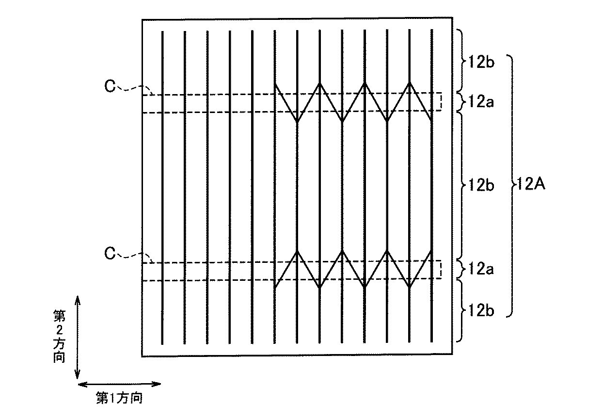
例えば、上記実施形態では、第1及び第2細線電極を第2方向に沿ってライン状に形成したが、細線電極の形状はこれに限らない。例えば、波線状の細線電極を格子状に形成することができる。 For example, in the above embodiment, the first and second thin wire electrodes are formed in a line shape along the second direction, but the shape of the thin wire electrode is not limited to this. For example, wavy thin wire electrodes can be formed in a lattice shape.
また、上記第1実施形態では、2本の第2細線電極13Aを1本に結合させたが、3本以上の第2細線電極13Aを1本に結合させてもよい。
In the first embodiment, two second
また、上記第2実施形態では、1本の第1細線電極12Aを3本に分岐させたが、2本又は4本以上に分岐させてもよい。
In the second embodiment, one first
また、上記第2実施形態では、領域Cから離間した位置において第1細線電極12Aを分岐させたが、領域C内で分岐されていてもよい。具体的には、図6に示すように第1接続部12aを形成することができる。また、図7に示すように、分岐した部分は第1方向に沿っておらず、ジグザグ状に形成されていてもよい。また、第1細線電極12Aを領域C内で分岐させる場合には、配線材5の一端部が圧着される領域で分岐させることが好ましい。これによって、配線材5の一端部から剥離が発生することを抑制することができる。
In the second embodiment, the first
また、上記第3実施形態では、島状部材14として絶縁性を有する部材により形成したが、細線電極と同様の導電性ペーストを用いて島状部材14を形成してもよい。
Moreover, in the said 3rd Embodiment, although formed with the member which has insulation as the island-shaped
また、上記第2乃至第4実施形態では、第2電極13は、複数本の第2細線電極13Aを有することとしたが、第2電極13の形状はこれに限られるものではない。例えば、第2電極13は、第2主面(裏面)B略全面に形成された電極であってもよい。
In the second to fourth embodiments, the second electrode 13 includes a plurality of second
このように、本発明はここでは記載していない様々な実施形態等を含むことは勿論である。従って、本発明の技術的範囲は上記の説明から妥当な特許請求の範囲に係る発明特定事項によってのみ定められるものである。 As described above, the present invention naturally includes various embodiments not described herein. Therefore, the technical scope of the present invention is defined only by the invention specifying matters according to the scope of claims reasonable from the above description.
以下、本発明に係る太陽電池モジュールの実施例について具体的に説明するが、本発明は、下記の実施例に示したものに限定されるものではなく、その要旨を変更しない範囲において、適宜変更して実施することができるものである。 Hereinafter, examples of the solar cell module according to the present invention will be specifically described. However, the present invention is not limited to those shown in the following examples, and may be appropriately changed within the scope not changing the gist thereof. Can be implemented.
(実施例1)
まず、寸法108mm角、厚み150μm、抵抗率1Ωcmのn型単結晶シリコン基板を準備した。Example 1
First, an n-type single crystal silicon substrate having a size of 108 mm square, a thickness of 150 μm, and a resistivity of 1 Ωcm was prepared.
次に、RFプラズマCVD法を用いて、基板の受光面上に、厚み5nmのi型非結晶シリコン層と厚み5nmのp型非晶質シリコン層とを順次形成した。続いて、基板の裏面上に、厚み5nmのi型非結晶シリコン層と厚み5nmのn型非晶質シリコン層とを順次形成した。RFプラズマCVD装置の条件設定は、周波数13.56MHz、形成温度100〜200℃、反応圧力20〜80Pa、RFパワー10〜100Wとした。 Next, an i-type amorphous silicon layer having a thickness of 5 nm and a p-type amorphous silicon layer having a thickness of 5 nm were sequentially formed on the light receiving surface of the substrate by using an RF plasma CVD method. Subsequently, an i-type amorphous silicon layer having a thickness of 5 nm and an n-type amorphous silicon layer having a thickness of 5 nm were sequentially formed on the back surface of the substrate. The conditions of the RF plasma CVD apparatus were set to a frequency of 13.56 MHz, a forming temperature of 100 to 200 ° C., a reaction pressure of 20 to 80 Pa, and an RF power of 10 to 100 W.
次に、マグネトロンスパッタ法を用いて、p型及びn型非晶質シリコン層上に、厚み100nmのITO膜を形成した。スパッタ装置の条件設定は、形成温度50〜200℃、Arガス流量200sccm、酸素ガス流量50sccm、パワー0.5〜3kW、磁場強度500〜3000ガウスとした。以上により光電変換部が作製された。 Next, an ITO film having a thickness of 100 nm was formed on the p-type and n-type amorphous silicon layers by using a magnetron sputtering method. The sputtering apparatus was set to a forming temperature of 50 to 200 ° C., an Ar gas flow rate of 200 sccm, an oxygen gas flow rate of 50 sccm, a power of 0.5 to 3 kW, and a magnetic field strength of 500 to 3000 gauss. The photoelectric conversion part was produced by the above.
次に、スクリーン印刷法を用いて、太陽電池の受光面上に、エポキシ系熱硬化型銀ペーストを図3(a)に示すパターンで印刷した。具体的には、52本の細線電極(幅100μm)を2mm間隔で形成した。150℃で5分間加熱することにより銀ペーストを仮硬化させた。 Next, an epoxy thermosetting silver paste was printed with a pattern shown in FIG. 3A on the light-receiving surface of the solar cell using a screen printing method. Specifically, 52 thin wire electrodes (width 100 μm) were formed at intervals of 2 mm. The silver paste was temporarily cured by heating at 150 ° C. for 5 minutes.
次に、太陽電池の裏面上に、エポキシ系熱硬化型銀ペーストを図3(b)に示すパターンで印刷した。具体的には、104本の細線電極(幅100μm)を1mm間隔で形成するとともに、配線材を接続する領域では、104本の細線電極を2本一組に結合することにより、52本の細線電極を2mm間隔で形成した。次に、200℃で1時間加熱することにより受光面上及び裏面上の銀ペーストを硬化させた。 Next, an epoxy thermosetting silver paste was printed on the back surface of the solar cell in the pattern shown in FIG. Specifically, 104 fine wire electrodes (width 100 μm) are formed at intervals of 1 mm, and in the region where the wiring material is connected, the 104 fine wire electrodes are joined together to form a set of 52 fine wires. Electrodes were formed at 2 mm intervals. Next, the silver paste on the light receiving surface and the back surface was cured by heating at 200 ° C. for 1 hour.
次に、ディスペンサーを用いて、ニッケル粒子を約5体積%含むエポキシ樹脂を、受光面上及び裏面上のうち配線材を接続する領域に厚み30μmで塗布した。なお、エポキシ樹脂を塗布する代わりに、テープ状に成形されたエポキシ樹脂を、受光面上及び裏面上のうち配線材を接続する領域に配置してもよい。 Next, using a dispenser, an epoxy resin containing about 5% by volume of nickel particles was applied at a thickness of 30 μm on the light receiving surface and the back surface to the region where the wiring material was connected. Instead of applying the epoxy resin, an epoxy resin formed in a tape shape may be arranged on the light receiving surface and the back surface in the region where the wiring material is connected.
次に、塗布したエポキシ樹脂上に配線材を配置し、約2MPaで加圧しながら200℃で約1時間加熱した。これにより、配線材に細線電極を食込ませるとともに、エポキシ樹脂を硬化させた。これを繰返すことにより太陽電池ストリングを作製した。 Next, a wiring material was placed on the applied epoxy resin and heated at 200 ° C. for about 1 hour while being pressurized at about 2 MPa. As a result, the thin wire electrode was bitten into the wiring material and the epoxy resin was cured. By repeating this, a solar cell string was produced.
次に、ガラスとPETフィルムの間に配置した太陽電池ストリングをEVAにより封止した。以上のようにして、実施例1に係る太陽電池モジュールを1000枚作製した。 Next, the solar cell string disposed between the glass and the PET film was sealed with EVA. As described above, 1000 solar cell modules according to Example 1 were manufactured.
(実施例2)
次に、実施例2に係る太陽電池モジュールを1000枚作製した。実施例2と上記実施例1との相違点は、銀ペーストを図4に示すパターンで印刷した点である。(Example 2)
Next, 1000 solar cell modules according to Example 2 were produced. The difference between Example 2 and Example 1 is that the silver paste was printed in the pattern shown in FIG.
具体的には、スクリーン印刷法を用いて、太陽電池の受光面上に、エポキシ系熱硬化型銀ペーストを図4(a)に示すパターンで印刷した。具体的には、52本の細線電極(幅100μm)を2mm間隔で形成するとともに、配線材を接続する領域では、1本の細線電極を2本に分岐させることにより、104本の細線電極を1mm間隔で形成した。 Specifically, an epoxy thermosetting silver paste was printed with a pattern shown in FIG. 4A on the light-receiving surface of the solar cell using a screen printing method. Specifically, 52 fine wire electrodes (width: 100 μm) are formed at intervals of 2 mm, and in the region where the wiring material is connected, one fine wire electrode is branched into two, so that 104 fine wire electrodes are formed. They were formed at 1 mm intervals.
また、太陽電池の裏面上に、エポキシ系熱硬化型銀ペーストを図4(b)に示すパターンで印刷した。具体的には、104本の細線電極(幅100μm)を1mm間隔で形成した。その他の点は、上記第1実施例と同様である。 Moreover, the epoxy thermosetting silver paste was printed on the back surface of the solar cell with the pattern shown in FIG. Specifically, 104 fine wire electrodes (width 100 μm) were formed at 1 mm intervals. The other points are the same as in the first embodiment.
(比較例)
次に、比較例1に係る太陽電池モジュールを1000枚作製した。比較例1と上記実施例1との相違点は、配線材を接続する領域において細線電極を分岐又は結合させない点である。(Comparative example)
Next, 1000 solar cell modules according to Comparative Example 1 were produced. The difference between Comparative Example 1 and Example 1 is that the thin wire electrode is not branched or joined in the region where the wiring material is connected.
すなわち、比較例では、直線状の細線電極を、受光面上に52本、裏面上に104本形成した。その他の点は上記第1実施例と同様である。 That is, in the comparative example, 52 linear thin wire electrodes were formed on the light receiving surface and 104 on the back surface. The other points are the same as in the first embodiment.
(温度サイクル試験)
実施例1、実施例2及び比較例に係る太陽電池について、恒温槽を用いて温度サイクル試験を行い、試験後における太陽電池の出力低下率を比較した。測定結果を下表に示す。なお、下表中の数値は、1000枚の太陽電池についての平均値である。(Temperature cycle test)
About the solar cell which concerns on Example 1, Example 2, and a comparative example, the temperature cycle test was done using the thermostat, and the output reduction rate of the solar cell after a test was compared. The measurement results are shown in the table below. In addition, the numerical value in the following table | surface is an average value about 1000 solar cells.
なお、温度サイクル試験は、JIS C 8917の規定に準拠して行った。具体的には、各サンプルを恒温槽内に保持し、45分かけて25℃から90℃まで上昇させ、この温度で90分間保持し、次いで90分かけて−40℃まで降下させ、この温度で90分間保持し、さらに45分かけて25℃まで上昇させる。これを1サイクル(6時間)として600サイクル行った。
上表に示す通り、実施例1及び2に係る太陽電池の出力低下率は、比較例に係る太陽電池よりも小さかった。 As shown in the above table, the output reduction rate of the solar cells according to Examples 1 and 2 was smaller than that of the solar cell according to the comparative example.
これは、実施例1に係る太陽電池において、裏面のうち配線材接続領域における単位面積あたりの電極形成面積を、受光面に近づけたためである。また、実施例2に係る太陽電池において、受光面のうち配線材接続領域における単位面積あたりの電極形成面積を、裏面に近づけたためである。すなわち、実施例1及び2係る太陽電池では、上記第1の関係((v/w)<1)と、上記第2の関係((v/w)<(x/y))とが成立する。 This is because, in the solar cell according to Example 1, the electrode formation area per unit area in the wiring material connection region on the back surface was brought close to the light receiving surface. Further, in the solar cell according to Example 2, the electrode formation area per unit area in the wiring material connection region on the light receiving surface was brought close to the back surface. That is, in the solar cells according to Examples 1 and 2, the first relationship ((v / w) <1) and the second relationship ((v / w) <(x / y)) are established. .
一方、比較例に係る太陽電池では、上記第2の関係((v/w)<(x/y))が成立しておらず、(v/w)=(x/y)の関係が成立する。そのため、裏面上の細線電極の配線材への食込み量は、受光面上の細線電極よりも小さかった。その結果、配線材よりも大きな線膨張係数を有する封止材(EVA)から温度変化に応じた応力がかかることにより、裏面上の細線電極と配線材との接続不良が生じた。 On the other hand, in the solar cell according to the comparative example, the second relationship ((v / w) <(x / y)) is not established, and the relationship (v / w) = (x / y) is established. To do. For this reason, the amount of the fine wire electrode on the back surface digged into the wiring material was smaller than that of the fine wire electrode on the light receiving surface. As a result, a stress corresponding to a temperature change is applied from a sealing material (EVA) having a larger linear expansion coefficient than that of the wiring material, resulting in poor connection between the thin wire electrode on the back surface and the wiring material.
以上より、第1の関係((v/w)<1)が成立する場合において、第2の関係((v/w)<(x/y))を成立させることにより、裏面上の細線電極と配線材との電気的、機械的な接続を良好に維持できることが確認された。 As described above, when the first relationship ((v / w) <1) is established, the thin wire electrode on the back surface is established by establishing the second relationship ((v / w) <(x / y)). It was confirmed that the electrical and mechanical connection between and the wiring material can be maintained well.
以上のように、本発明によれば、太陽電池の裏面上に形成される細線電極と配線材との良好な接続を維持できる太陽電池モジュールを提供することができるため、太陽光発電分野において有用である。 As described above, according to the present invention, it is possible to provide a solar cell module that can maintain a good connection between the thin wire electrode formed on the back surface of the solar cell and the wiring material, and thus is useful in the photovoltaic power generation field. It is.
Claims (7)
前記太陽電池の受光面の第1領域を覆う一の配線材と、
前記太陽電池の前記受光面の反対側に設けられる裏面の第2領域を覆う他の配線材と、を備え、
前記太陽電池は、
前記受光面上に形成される複数本の第1細線電極を少なくとも含む第1電極と、
前記裏面上に形成される第2電極と、
を有し、
前記第1電極は、
前記第1領域内に設けられ、前記一の配線材に接続される第1接続部と、
前記第1領域外に設けられ、前記一の配線材から露出する一群の第1露出部と、
を有し、
前記第2電極は、
前記第2領域内に設けられ、前記他の配線材に接続される第2接続部と、
前記第2領域外に設けられ、前記他の配線材から露出する第2露出部と、
を有し、
前記受光面の面積に対する前記第1露出部が形成される面積の比率である第1比率は、前記裏面の面積に対する前記第2露出部が形成される面積の比率である第2比率より小さく、
前記第1比率の前記第2比率に対する比は、前記受光面のうち前記第1領域の面積に対する前記第1接続部の面積の比率である第3比率の、前記裏面のうち前記第2領域の面積に対する前記第2接続部の面積の比率である第4比率に対する比よりも小さく、
前記第3比率及び前記第4比率のうち少なくともいずれか一方は1より小さい
ことを特徴とする太陽電池モジュール。 Solar cells,
One wiring material covering the first region of the light receiving surface of the solar cell;
Another wiring material covering the second region of the back surface provided on the opposite side of the light receiving surface of the solar cell,
The solar cell is
A first electrode including at least a plurality of first thin wire electrodes formed on the light receiving surface;
A second electrode formed on the back surface;
Have
The first electrode is
A first connection portion provided in the first region and connected to the one wiring member;
A group of first exposed portions provided outside the first region and exposed from the one wiring material;
Have
The second electrode is
A second connection portion provided in the second region and connected to the other wiring material;
A second exposed portion provided outside the second region and exposed from the other wiring material;
Have
The first ratio, which is the ratio of the area where the first exposed portion is formed to the area of the light receiving surface, is smaller than the second ratio, which is the ratio of the area where the second exposed portion is formed to the area of the back surface,
The ratio of the first ratio to the second ratio is a third ratio, which is a ratio of the area of the first connection portion to the area of the first region of the light receiving surface, and of the second region of the back surface. Smaller than the ratio to the fourth ratio, which is the ratio of the area of the second connection part to the area,
A solar cell module, wherein at least one of the third ratio and the fourth ratio is smaller than one .
前記複数本の第2細線電極は、前記第2接続部と前記第2露出部とを有する
ことを特徴とする請求項1に記載の太陽電池モジュール。 The second electrode has the plurality of second thin wire electrodes,
2. The solar cell module according to claim 1, wherein the plurality of second thin wire electrodes include the second connection portion and the second exposed portion.
ことを特徴とする請求項1又は2に記載の太陽電池モジュール。 The solar cell module according to claim 1, wherein the first connection portion is connected in direct contact with the one wiring member.
ことを特徴とする請求項1又は2に記載の太陽電池モジュール。 The solar cell module according to claim 1 or 2, wherein the second connection portion is connected in direct contact with the other wiring member.
ことを特徴とする請求項2に記載の太陽電池モジュール。 3. The solar cell module according to claim 2, wherein at least two second thin wire electrodes among the plurality of second thin wire electrodes are combined into one in the second region.
ことを特徴とする請求項1又は2に記載の太陽電池モジュール。 3. The solar cell module according to claim 1, wherein at least one first thin wire electrode among the plurality of first thin wire electrodes is branched into a plurality of wires in the first region. 4.
ことを特徴とする請求項1又は2に記載の太陽電池モジュール。 The solar cell module according to claim 1, wherein the first electrode includes an island-shaped member formed in an island shape in the first region.
Priority Applications (1)
| Application Number | Priority Date | Filing Date | Title |
|---|---|---|---|
| JP2009552536A JP5367587B2 (en) | 2008-02-08 | 2009-02-06 | Solar cell module and solar cell |
Applications Claiming Priority (4)
| Application Number | Priority Date | Filing Date | Title |
|---|---|---|---|
| JP2008029421 | 2008-02-08 | ||
| JP2008029421 | 2008-02-08 | ||
| PCT/JP2009/052044 WO2009099179A1 (en) | 2008-02-08 | 2009-02-06 | Solar cell module and solar cell |
| JP2009552536A JP5367587B2 (en) | 2008-02-08 | 2009-02-06 | Solar cell module and solar cell |
Publications (2)
| Publication Number | Publication Date |
|---|---|
| JPWO2009099179A1 JPWO2009099179A1 (en) | 2011-05-26 |
| JP5367587B2 true JP5367587B2 (en) | 2013-12-11 |
Family
ID=40952251
Family Applications (1)
| Application Number | Title | Priority Date | Filing Date |
|---|---|---|---|
| JP2009552536A Active JP5367587B2 (en) | 2008-02-08 | 2009-02-06 | Solar cell module and solar cell |
Country Status (6)
| Country | Link |
|---|---|
| US (1) | US20110011454A1 (en) |
| EP (1) | EP2267794A4 (en) |
| JP (1) | JP5367587B2 (en) |
| KR (1) | KR101485623B1 (en) |
| CN (1) | CN101939847B (en) |
| WO (1) | WO2009099179A1 (en) |
Families Citing this family (31)
| Publication number | Priority date | Publication date | Assignee | Title |
|---|---|---|---|---|
| JP5306112B2 (en) * | 2009-02-17 | 2013-10-02 | 三洋電機株式会社 | Solar cell and solar cell module |
| EP2356695B1 (en) | 2009-03-03 | 2018-11-21 | LG Electronics Inc. | Solar cell |
| JP5923732B2 (en) * | 2009-11-20 | 2016-05-25 | パナソニックIpマネジメント株式会社 | Solar cell module |
| JP5289291B2 (en) * | 2009-12-01 | 2013-09-11 | デクセリアルズ株式会社 | Electronic component manufacturing method, electronic component and conductive film |
| JP5479222B2 (en) * | 2010-05-25 | 2014-04-23 | 三洋電機株式会社 | Solar cell module |
| JP5479228B2 (en) * | 2010-05-28 | 2014-04-23 | 三洋電機株式会社 | Solar cell module |
| CN101867321B (en) * | 2010-05-31 | 2013-04-03 | 江西赛维Ldk太阳能高科技有限公司 | Solar cell string and solar cell component for ground power generation and solar cell plate thereof |
| WO2012002216A1 (en) * | 2010-06-30 | 2012-01-05 | 三洋電機株式会社 | Solar cell module |
| KR101045860B1 (en) * | 2010-08-11 | 2011-07-01 | 엘지전자 주식회사 | Solar panels |
| KR101621989B1 (en) * | 2011-01-27 | 2016-05-17 | 엘지전자 주식회사 | Solar cell panel |
| WO2012111108A1 (en) * | 2011-02-16 | 2012-08-23 | 三菱電機株式会社 | Solar cell, solar cell module and method of joining lead wire of solar cell |
| CN202513163U (en) * | 2011-03-08 | 2012-10-31 | 日立化成工业株式会社 | Solar cell assembly |
| US20120227785A1 (en) * | 2011-03-08 | 2012-09-13 | Hitachi Chemical Company, Ltd. | Solar battery cell, solar battery module, method of making solar battery cell and method of making solar battery module |
| TW201246584A (en) * | 2011-03-08 | 2012-11-16 | Hitachi Chemical Co Ltd | Solar battery cell, solar battery module, fabricating method of solar battery cell and fabricating method of solar battery module |
| CN102148275A (en) * | 2011-03-16 | 2011-08-10 | 常州天合光能有限公司 | Solar battery component |
| US9455359B2 (en) | 2011-05-31 | 2016-09-27 | Hitachi Chemical Company, Ltd. | Solar battery cell, solar battery module and method of making solar battery module |
| JP5967512B2 (en) * | 2011-06-30 | 2016-08-10 | パナソニックIpマネジメント株式会社 | Solar cell module |
| JP2013030689A (en) * | 2011-07-29 | 2013-02-07 | Sumitomo Electric Device Innovations Inc | Semiconductor light-receiving device |
| KR101969032B1 (en) * | 2011-09-07 | 2019-04-15 | 엘지전자 주식회사 | Solar cell and manufacturing method thereof |
| WO2013039158A1 (en) * | 2011-09-13 | 2013-03-21 | 京セラ株式会社 | Solar cell module |
| WO2013069425A1 (en) * | 2011-11-09 | 2013-05-16 | 三菱電機株式会社 | Solar cell module and manufacturing method therefor |
| WO2014002268A1 (en) * | 2012-06-29 | 2014-01-03 | 三洋電機株式会社 | Solar cell module and solar cell module manufacturing method |
| CN103681891A (en) * | 2012-09-25 | 2014-03-26 | 茂迪(苏州)新能源有限公司 | A solar cell and a module thereof |
| CN103165693B (en) * | 2013-02-18 | 2016-03-16 | 友达光电股份有限公司 | solar module |
| TWI527251B (en) * | 2013-02-27 | 2016-03-21 | 茂迪股份有限公司 | Solar cell and its module |
| US10263131B2 (en) | 2014-04-07 | 2019-04-16 | Solaero Technologies Corp. | Parallel interconnection of neighboring solar cells with dual common back planes |
| KR20160038694A (en) * | 2014-09-30 | 2016-04-07 | 엘지전자 주식회사 | Solar cell and solar cell panel including the same |
| KR101666630B1 (en) * | 2014-10-29 | 2016-10-18 | 한국에너지기술연구원 | Method for Producing Solar Cell Module Using Conductive Paste |
| JP6455099B2 (en) * | 2014-11-27 | 2019-01-23 | 日立化成株式会社 | Solar cell unit and method for manufacturing solar cell unit |
| ES2744540T3 (en) * | 2014-12-05 | 2020-02-25 | Hoffmann La Roche | Anti-CD79b antibodies and usage procedures |
| US11532765B2 (en) * | 2015-04-30 | 2022-12-20 | Shangrao Jinko Solar Technology Development Co., Ltd | Solar cell and solar cell panel including the same |
Citations (4)
| Publication number | Priority date | Publication date | Assignee | Title |
|---|---|---|---|---|
| JP2006013173A (en) * | 2004-06-25 | 2006-01-12 | Kyocera Corp | Solar cell module |
| JP2006237363A (en) * | 2005-02-25 | 2006-09-07 | Sanyo Electric Co Ltd | Photovoltaic element |
| JP2007103535A (en) * | 2005-09-30 | 2007-04-19 | Sanyo Electric Co Ltd | Solar cell module |
| JP2007200970A (en) * | 2006-01-24 | 2007-08-09 | Sanyo Electric Co Ltd | Photovoltaic module |
Family Cites Families (6)
| Publication number | Priority date | Publication date | Assignee | Title |
|---|---|---|---|---|
| JP2002076400A (en) * | 2000-08-30 | 2002-03-15 | Shin Etsu Handotai Co Ltd | Solar cell and method for manufacturing solar cell |
| FR2831714B1 (en) * | 2001-10-30 | 2004-06-18 | Dgtec | ASSEMBLY OF PHOTOVOLTAIC CELLS |
| JP2002359388A (en) | 2002-05-28 | 2002-12-13 | Kyocera Corp | Solar cell device |
| JP2005101519A (en) | 2003-09-05 | 2005-04-14 | Hitachi Chem Co Ltd | Solar cell unit and solar cell module |
| US8440907B2 (en) * | 2006-04-14 | 2013-05-14 | Sharp Kabushiki Kaisha | Solar cell, solar cell string and solar cell module |
| JP2007305876A (en) | 2006-05-12 | 2007-11-22 | Matsushita Electric Ind Co Ltd | Solar cell module |
-
2009
- 2009-02-06 US US12/866,020 patent/US20110011454A1/en not_active Abandoned
- 2009-02-06 JP JP2009552536A patent/JP5367587B2/en active Active
- 2009-02-06 KR KR1020107017677A patent/KR101485623B1/en active Active
- 2009-02-06 EP EP09709427.0A patent/EP2267794A4/en not_active Withdrawn
- 2009-02-06 CN CN2009801044752A patent/CN101939847B/en active Active
- 2009-02-06 WO PCT/JP2009/052044 patent/WO2009099179A1/en not_active Ceased
Patent Citations (4)
| Publication number | Priority date | Publication date | Assignee | Title |
|---|---|---|---|---|
| JP2006013173A (en) * | 2004-06-25 | 2006-01-12 | Kyocera Corp | Solar cell module |
| JP2006237363A (en) * | 2005-02-25 | 2006-09-07 | Sanyo Electric Co Ltd | Photovoltaic element |
| JP2007103535A (en) * | 2005-09-30 | 2007-04-19 | Sanyo Electric Co Ltd | Solar cell module |
| JP2007200970A (en) * | 2006-01-24 | 2007-08-09 | Sanyo Electric Co Ltd | Photovoltaic module |
Also Published As
| Publication number | Publication date |
|---|---|
| EP2267794A1 (en) | 2010-12-29 |
| EP2267794A4 (en) | 2015-10-14 |
| US20110011454A1 (en) | 2011-01-20 |
| JPWO2009099179A1 (en) | 2011-05-26 |
| CN101939847A (en) | 2011-01-05 |
| WO2009099179A1 (en) | 2009-08-13 |
| CN101939847B (en) | 2012-04-25 |
| KR101485623B1 (en) | 2015-01-23 |
| KR20100124715A (en) | 2010-11-29 |
Similar Documents
| Publication | Publication Date | Title |
|---|---|---|
| JP5367587B2 (en) | Solar cell module and solar cell | |
| JP4429306B2 (en) | Solar cell and solar cell module | |
| US8298363B2 (en) | Method of manufacturing solar cell module | |
| JP5410050B2 (en) | Solar cell module | |
| US8497419B2 (en) | Solar cell module | |
| TWI488315B (en) | Solar battery module and manufacturing method thereof | |
| US20100243024A1 (en) | Solar cell, solar cell module and solar cell system | |
| JP6280692B2 (en) | SOLAR CELL MODULE AND CRYSTAL SOLAR CELL MODULE MANUFACTURING METHOD | |
| CN104253169B (en) | Without main grid, high efficiency back contact solar cell module, assembly and preparation technology | |
| CN104269462B (en) | Back contact solar cell back sheet without main grids, back contact solar cell assembly without main grids and manufacturing technology | |
| JP2011181966A (en) | Solar battery cell and solar battery module | |
| JP5052154B2 (en) | Manufacturing method of solar cell module | |
| JP5100206B2 (en) | Solar cell module | |
| JP2014157874A (en) | Solar battery module and method of manufacturing the same | |
| US20120073621A1 (en) | Solar cell and solar cell module | |
| WO2014050193A1 (en) | Photoelectric conversion module | |
| JP2011054660A (en) | Solar-cell string and solar-cell module using the same | |
| JP5100216B2 (en) | Solar cell group and manufacturing method thereof, solar cell module including solar cell group and manufacturing method thereof | |
| JP5516566B2 (en) | Solar cell module and manufacturing method thereof | |
| JP5851355B2 (en) | Light receiving element module and manufacturing method thereof |
Legal Events
| Date | Code | Title | Description |
|---|---|---|---|
| A621 | Written request for application examination |
Free format text: JAPANESE INTERMEDIATE CODE: A621 Effective date: 20120127 |
|
| A131 | Notification of reasons for refusal |
Free format text: JAPANESE INTERMEDIATE CODE: A131 Effective date: 20121204 |
|
| A521 | Request for written amendment filed |
Free format text: JAPANESE INTERMEDIATE CODE: A523 Effective date: 20130125 |
|
| A131 | Notification of reasons for refusal |
Free format text: JAPANESE INTERMEDIATE CODE: A131 Effective date: 20130423 |
|
| A521 | Request for written amendment filed |
Free format text: JAPANESE INTERMEDIATE CODE: A523 Effective date: 20130528 |
|
| TRDD | Decision of grant or rejection written | ||
| A01 | Written decision to grant a patent or to grant a registration (utility model) |
Free format text: JAPANESE INTERMEDIATE CODE: A01 Effective date: 20130813 |
|
| A61 | First payment of annual fees (during grant procedure) |
Free format text: JAPANESE INTERMEDIATE CODE: A61 Effective date: 20130911 |
|
| R151 | Written notification of patent or utility model registration |
Ref document number: 5367587 Country of ref document: JP Free format text: JAPANESE INTERMEDIATE CODE: R151 |
|
| R250 | Receipt of annual fees |
Free format text: JAPANESE INTERMEDIATE CODE: R250 |
|
| R250 | Receipt of annual fees |
Free format text: JAPANESE INTERMEDIATE CODE: R250 |
|
| S531 | Written request for registration of change of domicile |
Free format text: JAPANESE INTERMEDIATE CODE: R313531 |